KR100668348B1 - Nonvolatile Memory Device and Manufacturing Method Thereof - Google Patents
Nonvolatile Memory Device and Manufacturing Method ThereofDownload PDFInfo
- Publication number
- KR100668348B1 KR100668348B1KR1020050108125AKR20050108125AKR100668348B1KR 100668348 B1KR100668348 B1KR 100668348B1KR 1020050108125 AKR1020050108125 AKR 1020050108125AKR 20050108125 AKR20050108125 AKR 20050108125AKR 100668348 B1KR100668348 B1KR 100668348B1
- Authority
- KR
- South Korea
- Prior art keywords
- memory device
- electrode
- manufacturing
- nonvolatile memory
- oxide
- Prior art date
- Legal status (The legal status is an assumption and is not a legal conclusion. Google has not performed a legal analysis and makes no representation as to the accuracy of the status listed.)
- Expired - Fee Related
Links
Images


Classifications
- H—ELECTRICITY
- H10—SEMICONDUCTOR DEVICES; ELECTRIC SOLID-STATE DEVICES NOT OTHERWISE PROVIDED FOR
- H10B—ELECTRONIC MEMORY DEVICES
- H10B63/00—Resistance change memory devices, e.g. resistive RAM [ReRAM] devices
- H10B63/30—Resistance change memory devices, e.g. resistive RAM [ReRAM] devices comprising selection components having three or more electrodes, e.g. transistors
- H—ELECTRICITY
- H10—SEMICONDUCTOR DEVICES; ELECTRIC SOLID-STATE DEVICES NOT OTHERWISE PROVIDED FOR
- H10N—ELECTRIC SOLID-STATE DEVICES NOT OTHERWISE PROVIDED FOR
- H10N70/00—Solid-state devices having no potential barriers, and specially adapted for rectifying, amplifying, oscillating or switching
- H10N70/20—Multistable switching devices, e.g. memristors
- H—ELECTRICITY
- H10—SEMICONDUCTOR DEVICES; ELECTRIC SOLID-STATE DEVICES NOT OTHERWISE PROVIDED FOR
- H10N—ELECTRIC SOLID-STATE DEVICES NOT OTHERWISE PROVIDED FOR
- H10N70/00—Solid-state devices having no potential barriers, and specially adapted for rectifying, amplifying, oscillating or switching
- H10N70/801—Constructional details of multistable switching devices
- H10N70/821—Device geometry
- H10N70/826—Device geometry adapted for essentially vertical current flow, e.g. sandwich or pillar type devices
- H—ELECTRICITY
- H10—SEMICONDUCTOR DEVICES; ELECTRIC SOLID-STATE DEVICES NOT OTHERWISE PROVIDED FOR
- H10N—ELECTRIC SOLID-STATE DEVICES NOT OTHERWISE PROVIDED FOR
- H10N70/00—Solid-state devices having no potential barriers, and specially adapted for rectifying, amplifying, oscillating or switching
- H10N70/801—Constructional details of multistable switching devices
- H10N70/841—Electrodes
- H—ELECTRICITY
- H10—SEMICONDUCTOR DEVICES; ELECTRIC SOLID-STATE DEVICES NOT OTHERWISE PROVIDED FOR
- H10N—ELECTRIC SOLID-STATE DEVICES NOT OTHERWISE PROVIDED FOR
- H10N70/00—Solid-state devices having no potential barriers, and specially adapted for rectifying, amplifying, oscillating or switching
- H10N70/801—Constructional details of multistable switching devices
- H10N70/881—Switching materials
- H10N70/882—Compounds of sulfur, selenium or tellurium, e.g. chalcogenides
- H10N70/8825—Selenides, e.g. GeSe
- H—ELECTRICITY
- H10—SEMICONDUCTOR DEVICES; ELECTRIC SOLID-STATE DEVICES NOT OTHERWISE PROVIDED FOR
- H10N—ELECTRIC SOLID-STATE DEVICES NOT OTHERWISE PROVIDED FOR
- H10N70/00—Solid-state devices having no potential barriers, and specially adapted for rectifying, amplifying, oscillating or switching
- H10N70/801—Constructional details of multistable switching devices
- H10N70/881—Switching materials
- H10N70/882—Compounds of sulfur, selenium or tellurium, e.g. chalcogenides
- H10N70/8828—Tellurides, e.g. GeSbTe
- H—ELECTRICITY
- H10—SEMICONDUCTOR DEVICES; ELECTRIC SOLID-STATE DEVICES NOT OTHERWISE PROVIDED FOR
- H10N—ELECTRIC SOLID-STATE DEVICES NOT OTHERWISE PROVIDED FOR
- H10N70/00—Solid-state devices having no potential barriers, and specially adapted for rectifying, amplifying, oscillating or switching
- H10N70/801—Constructional details of multistable switching devices
- H10N70/881—Switching materials
- H10N70/883—Oxides or nitrides
- H10N70/8833—Binary metal oxides, e.g. TaOx
Landscapes
- Semiconductor Memories (AREA)
Abstract
Translated fromKoreanDescription
Translated fromKorean도 1은 종래 비휘발성 메모리 소자의 개략적 단면도이다.1 is a schematic cross-sectional view of a conventional nonvolatile memory device.
도 2는 도 1에서 스토리지 노드의 스위칭 특성을 보여주는 그래프이다.FIG. 2 is a graph illustrating switching characteristics of a storage node in FIG. 1.
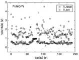
도 3a는 도 1에서 스토리지 노드에 인가되는 셋(set)/리셋(reset) 전압값 분포를 보여주는 그래프이다.3A is a graph illustrating a distribution of set / reset voltage values applied to a storage node in FIG. 1.
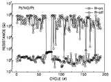
도 3b는 도 1에서 온(on)/오프(off) 상태에 따른 스토리지 노드의 저항값 분포를 보여주는 그래프이다.FIG. 3B is a graph illustrating a distribution of resistance values of storage nodes according to an on / off state of FIG. 1.
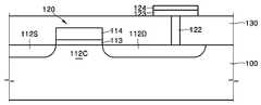
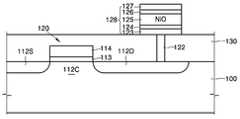
도 4는 본 발명의 실시예에 따른 비휘발성 메모리 소자의 개략적 단면도다.4 is a schematic cross-sectional view of a nonvolatile memory device according to an embodiment of the present invention.
도 5는 도 4에서 스토리지 노드의 스위칭 특성을 보여주는 그래프이다.FIG. 5 is a graph illustrating switching characteristics of a storage node in FIG. 4.
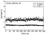
도 6a는 도 4에서 스토리지 노드에 인가되는 셋/리셋 전압값 분포를 보여주는 그래프이다.6A is a graph illustrating a distribution of set / reset voltage values applied to a storage node in FIG. 4.
도 6b는 도 6a의 히스토그램 그래프이다.FIG. 6B is a histogram graph of FIG. 6A.
도 7a는 도 4에서 온/오프 상태에 따른 스토리지 노드의 저항값 분포를 보여주는 그래프이다.FIG. 7A is a graph illustrating a distribution of resistance values of storage nodes according to on / off states of FIG. 4.
도 7b는 도 7a의 히스토그램 그래프이다.FIG. 7B is a histogram graph of FIG. 7A.
도 8a 내지 도 8e는 본 발명의 실시예에 따른 비휘발성 메모리 소자의 제조 방법을 보여주는 공정흐름도이다.8A through 8E are flowcharts illustrating a method of manufacturing a nonvolatile memory device according to an exemplary embodiment of the present invention.
< 도면의 주요부분에 대한 부호의 설명 ><Description of Symbols for Major Parts of Drawings>
100:기판 112S:소오스100:
112D:드레인 112C:채널112D:
113:게이트절연막 114:게이트전극113: gate insulating film 114: gate electrode
120:트랜지스터 122:콘택트플러그120: transistor 122: contact plug
123:제1 전극 124:제1 콘택트층123: first electrode 124: first contact layer
125:데이터 저장층 126:제2 콘택트층125: data storage layer 126: second contact layer
127:제2 전극 128:스토리지 노드127: second electrode 128: storage node
130:절연층 132:플레이트전극130: insulating layer 132: plate electrode
본 발명은 저항체를 이용한 비휘발성 메모리 소자에 관한 것으로, 보다 상세하게는 스토리지 노드에서 안정적인 메모리 스위칭 특성을 갖도록 그 구조가 개선된 비휘발성 메모리 소자 및 그 제조방법에 관한 것이다.BACKGROUND OF THE
종래 저항체(resistance material)를 이용한 비휘발성 메모리 소자로서 FRAM, MRAM 및 PRAM 등이 개발되었다. DRAM이나 플래시 메모리가 전하(charge)를 이용하여 이진정보를 저장하는 반면, 이들 소자들은 강유전체 물질의 분극현상(FRAM), 강자성체의 자화상태에 따른 MTJ(Magnetic Tunnel Junction) 박막의 저항 변화(MRAM), 상변화로 인한 저항변화(PRAM) 등을 이용하여 이진정보를 저장하는 특징을 가진다. 특히, 이들은 DRAM이 가지는 고집적 특성과 플래시 메모리가 가지는 비휘발성 특성을 모두 갖고 있어 종래의 휘발성이나 비휘발성 메모리를 대체할 만한 가능성이 있는 소자들로 주목된다.Conventionally, FRAM, MRAM, and PRAM have been developed as nonvolatile memory devices using a resistive material. While DRAM and flash memory store binary information by using charges, these devices have a resistance change (MRAM) of a magnetic tunnel junction junction (MTJ) thin film due to a polarization phenomenon (FRAM) of ferroelectric material and a magnetization state of ferromagnetic material. , Binary information is stored using resistance change (PRAM) due to phase change. In particular, they have both high-integration characteristics of DRAM and non-volatile characteristics of flash memory, and thus are attracting attention as devices that may replace conventional volatile or nonvolatile memories.
비휘발성 메모리 소자의 일례로, PRAM(phase-change RAM)은 GeSbTe와 같은 상변화(phase-change) 물질이 전기적인 펄스에 의한 국부적인 열발생에 의해 결정질(crystalline)과 비정질(amorphous) 상태로 변화하는 특성을 이용하여 이진정보를 기억하는 소자이다. PRAM은 이진정보를 기억하는 메모리셀이 상변화층과 레지스터(resistor) 및 스위치 트랜지스터로 구성된다. 상변화층은 이른바 GST(GeSbTe) 기반의 물질로서 갈코게나이드(chalcogenide)라는 명칭으로 불린다. 레지스터의 용도는 상변화층을 가열할 목적으로 쓰인다. 가열되는 정도에 따라 상변화층이 결정질과 비정질 상태로 상변화를 일으키게 되어 저항값이 달라지게 되고, 저항에 흐르는 전류로 인해 전압이 달라지게 되므로 이진정보를 저장 및 판독할 수 있게 된다.As an example of a nonvolatile memory device, phase-change RAM (PRAM) is a phase-change material such as GeSbTe in a crystalline and amorphous state by local heat generation by an electrical pulse. A device that stores binary information by using changing characteristics. In a PRAM, a memory cell that stores binary information includes a phase change layer, a resistor, and a switch transistor. The phase change layer is a so-called GST (GeSbTe) based material and is called a galcogenide. The purpose of the resistor is to heat the phase change layer. Depending on the degree of heating, the phase change layer causes a phase change in a crystalline and amorphous state, resulting in a change in resistance value, and a voltage change due to a current flowing through the resistance, so that binary information can be stored and read.
도 1은 종래 비휘발성 메모리 소자의 개략적 단면도이며, 도 2는 도 1에서 스토리지 노드의 스위칭 특성을 보여주는 그래프이다. 그리고, 도 3a는 도 1에서 스토리지 노드에 인가되는 셋(set)/리셋(reset) 전압값 분포를 보여주는 그래프이며, 도 3b는 도 1에서 온(on)/오프(off) 상태에 따른 스토리지 노드의 저항값 분포를 보여주는 그래프이다.1 is a schematic cross-sectional view of a conventional nonvolatile memory device, and FIG. 2 is a graph showing switching characteristics of a storage node in FIG. 1. 3A is a graph illustrating a distribution of set / reset voltage values applied to a storage node in FIG. 1, and FIG. 3B is a storage node according to an on / off state in FIG. 1. This graph shows the distribution of resistance values.
도 1을 참조하면, 종래 NiO 박막을 이용한 비휘발성 메모리 소자는 트랜지스터(20)와 이에 연결된 스토리지 노드(storage node, 28)를 구비한다. 상기 트랜지 스터(20)는 소오스(12s)와 드레인(12d)과 채널(12c) 및 게이트전극(14)을 포함한다. 상기 스토리지 노드(28)는 상부전극(27)과 하부전극(23) 및 이들 사이에 개재된 NiO 박막(25)을 포함하며, 상기 스토리지 노드(28)와 트랜지스터(20) 사이에 절연층(30)이 개재된다. 그리고, 상기 스토리지 노드(28)는 도전성의 콘택트플러그(contact plug, 22)에 의해 상기 트랜지스터(20)와 연결되며, 상기 상부전극(27) 위에 플레이트전극(32)이 배치된다.Referring to FIG. 1, a conventional nonvolatile memory device using a NiO thin film includes a
도시된 바와 같이 종래 메모리 소자의 스토리지 노드(28)는 M-I-M 메모리 셀 구조를 갖는다. 여기에서, M은 금속재질의 상부 및 하부전극을 지칭하며, I는 저항체 물질인 NiO층을 지칭한다. 기존의 M-I-M 메모리 셀 구조의 저항체 메모리소자에서는, 반복적인 스위칭시에 스토리지 노드에 인가되는 셋(set)/리셋(reset) 전압값(Vset, Vreset)의 분포편차가 크다(broad)는 문제점이 있었다. 또한, 반복 스위칭의 경우, 온(on)/오프(off) 상태에 따른 스토리지 노드의 저항값(Ron, Roff) 분포가 균일하지 못하다는 문제점이 있었다.As shown, the
이러한 문제점들로 인하여, 그 결과 종래 비휘발성 메모리 소자에서는 안정적인 메모리 스위칭 특성이 구현될 수 없었으며, 이러한 문제점들을 개선하기 위하여 종래 스토리지 노드의 구조를 개선할 필요성이 있었다.Due to these problems, as a result, stable memory switching characteristics could not be implemented in the conventional nonvolatile memory device, and there is a need to improve the structure of the conventional storage node in order to improve these problems.
본 발명이 이루고자 하는 기술적 과제는 상술한 종래기술의 문제점을 개선하기 위한 것으로, 스토리지 노드에서 안정적인 메모리 스위칭 특성을 갖도록 그 구 조가 개선된 비휘발성 메모리 소자 및 그 제조방법을 제공함에 있다.SUMMARY OF THE INVENTION The present invention has been made in an effort to improve the above-described problems of the related art, and to provide a nonvolatile memory device and a method of manufacturing the structure whose structure is improved to have stable memory switching characteristics in a storage node.
본 발명에 따른 비휘발성 메모리 소자는 스위칭 소자와 상기 스위칭 소자에 연결된 스토리지 노드를 구비하고,A nonvolatile memory device according to the present invention includes a switching device and a storage node connected to the switching device.
상기 스토리지 노드는,The storage node,
제1 전극과 제2 전극;A first electrode and a second electrode;
상기 제1 전극과 제2 전극 사이에 개재되는 것으로 전이금속 산화물 또는 알루미늄 산화물로 형성된 데이터 저장층; 및A data storage layer interposed between the first electrode and the second electrode and formed of a transition metal oxide or aluminum oxide; And
상기 데이터 저장층의 상면과 하면 중 적어도 어느 일면에 전도성 금속산화물로 형성되어 상기 데이터 저장층과 제1, 제2 전극 사이의 계면특성을 향상시키는 콘택트층(contact layer);을 포함한다. 여기에서, 상기 전도성 금속산화물은 IrO2, RuO2, SrRuO3, MoO2, OsO2, ReO2, RhO2, WO2및 ITO(Indium Tin Oxide)으로 이루어지는 그룹에서 선택된 어느 하나이다. 바람직하게, 상기 콘택트층은 10Å 내지 500Å 범위의 두께를 갖는다. 그리고, 상기 전이금속 산화물은 니켈(Ni), 니오븀(Nb), 티타늄(Ti), 지르코늄(Zr), 하프늄 (Hf), 코발트(Co), 철(Fe), 구리(Cu) 및 크롬(Cr)으로 이루어지는 그룹에서 선택된 어는 한 금속의 산화물이다. 또한, 상기 제1 및 제2 전극은 이리듐(Ir), 백금(Pt), 루테늄(Ru), 텅스텐(W), 티타늄나이트라이드(TiN) 및 폴리실리콘(poly-Si)으로 이루어지는 그룹에서 선택된 어느 하나의 물질로 형성된 것이다. 여기에서, 상기 스위칭 소자는 트랜지스터 또는 다이오드를 포 함한다.And a contact layer formed of a conductive metal oxide on at least one of an upper surface and a lower surface of the data storage layer to improve an interface property between the data storage layer and the first and second electrodes. Here, the conductive metal oxideIrO 2, RuO 2, SrRuO 3 ,
또한, 본 발명에 따른 비휘발성 메모리 소자의 제조방법은,In addition, the manufacturing method of the nonvolatile memory device according to the present invention,
스위칭 소자를 준비하는 단계;Preparing a switching device;
상기 스위칭 소자에 연결되는 제1 전극을 형성하는 단계;Forming a first electrode connected to the switching element;
상기 제1 전극 위에 전도성 금속산화물로 제1 콘택트층을 형성하는 단계;Forming a first contact layer of a conductive metal oxide on the first electrode;
상기 제1 콘택트층 위에 전이금속 산화물 또는 알루미늄 산화물로 데이터 저장층을 형성하는 단계; 및Forming a data storage layer of transition metal oxide or aluminum oxide on the first contact layer; And
상기 데이터 저장층 위에 제2 전극을 형성하는 단계;를 포함한다.And forming a second electrode on the data storage layer.
바람직하게, 상기 데이터 저장층을 형성하는 단계:와 제2 전극을 형성하는 단계: 사이에 상기 데이터 저장층 위에 전도성 금속산화물로 제2 콘택트층을 형성하는 단계;를 더 포함할 수 있다.Preferably, the method may further include forming a second contact layer with a conductive metal oxide on the data storage layer: forming the data storage layer: and forming the second electrode.
또한, 본 발명에 따른 비휘발성 메모리 소자의 제조방법은,In addition, the manufacturing method of the nonvolatile memory device according to the present invention,
스위칭 소자를 준비하는 단계;Preparing a switching device;
상기 스위칭 소자에 연결되는 제1 전극을 형성하는 단계;Forming a first electrode connected to the switching element;
상기 제1 전극 위에 전이금속 산화물 또는 알루미늄 산화물로 데이터 저장층을 형성하는 단계;Forming a data storage layer of transition metal oxide or aluminum oxide on the first electrode;
상기 데이터 저장층 위에 전도성 금속산화물로 콘택트층을 형성하는 단계; 및Forming a contact layer of a conductive metal oxide on the data storage layer; And
상기 콘택트층 위에 제2 전극을 형성하는 단계;를 포함한다.And forming a second electrode on the contact layer.
여기에서, 상기 전도성 금속산화물은 IrO2, RuO2, SrRuO3, MoO2, OsO2, ReO2, RhO2, WO2및 ITO(Indium Tin Oxide)으로 이루어지는 그룹에서 선택된 어느 하나이다. 바람직하게, 상기 제1 및 제2 콘택트층은 10Å 내지 500Å 범위의 두께로 형성된다. 그리고, 상기 전이금속 산화물은 니켈(Ni), 니오븀(Nb), 티타늄(Ti), 지르코늄(Zr), 하프늄 (Hf), 코발트(Co), 철(Fe), 구리(Cu) 및 크롬(Cr)으로 이루어지는 그룹에서 선택된 어는 한 금속의 산화물이다. 또한, 상기 제1 및 제2 전극은 이리듐(Ir), 백금(Pt), 루테늄(Ru), 텅스텐(W), 티타늄나이트라이드(TiN) 및 폴리실리콘(poly-Si)으로 이루어지는 그룹에서 선택된 어느 하나의 물질로 형성된다. 여기에서, 상기 스위칭 소자는 트랜지스터 또는 다이오드를 포함한다.Here, the conductive metal oxideIrO 2, RuO 2, SrRuO 3 ,
상기와 같은 구성을 갖는 비휘발성 메모리 소자는 스토리지 노드에서 안정적인 메모리 스위칭 특성을 가질 수 있다.The nonvolatile memory device having the above configuration may have stable memory switching characteristics in the storage node.
이하에서는, 본 발명에 따른 비휘발성 메모리 소자 및 그 제조방법의 바람직한 실시예를 첨부된 도면을 참조하여 상세히 설명한다. 이 과정에서 도면에 도시된 층이나 영역들의 두께는 상세한 설명을 위하여 과장되게 도시된 것이다.Hereinafter, exemplary embodiments of a nonvolatile memory device and a method of manufacturing the same according to the present invention will be described in detail with reference to the accompanying drawings. In this process, the thicknesses of the layers or regions illustrated in the drawings are exaggerated for the detailed description.
도 4는 본 발명의 실시예에 따른 비휘발성 메모리 소자의 개략적 단면도이며, 도 5는 도 4에서 스토리지 노드의 스위칭 특성을 보여주는 그래프이다.4 is a schematic cross-sectional view of a nonvolatile memory device according to an embodiment of the present invention, and FIG. 5 is a graph showing switching characteristics of a storage node in FIG. 4.
도 4 및 도 5를 함께 참조하면, 본 발명의 일실시예에 따른 비휘발성 메모리 소자는 스위칭 소자인 트랜지스터(120)와 상기 트랜지스터(120)에 연결된 스토리지 노드(128)를 구비한다. 그리고, 상기 스토리지 노드(128)와 트랜지스터(120) 사이 에 절연층(130)이 개재되며, 상기 스토리지 노드(128)는 도전성의 콘택플러그(contact plug, 122)에 의해 상기 트랜지스터 (120)와 연결된다. 그리고, 상기 스토리지 노드(128) 위에 플레이트전극(132)이 배치되어 상기 스토리지 노드(128)과 연결된다. 상기 트랜지스터(120)는 소오스(112s)와 드레인(112d)과 채널(112c) 및 게이트전극(114)을 포함하며, 이와 같은 반도체 트랜지스터(120)의 구조 및 형성방법은 널리 알려져 있으므로 이에 대한 상세한 설명은 생략하기로 한다. 또한, 여기에서 트랜지스터(120) 대신에 다른 스위칭 소자, 예를 들어 다이오드가 이용될 수 있으며, 이러한 다이오드의 구조 및 제조방법은 널리 알려져 있으므로 이에 대한 상세한 설명은 생략하기로 하고, 트랜지스터 스위치를 중심으로 본 발명의 실시예를 기술하기로 한다.4 and 5, a nonvolatile memory device according to an embodiment of the present invention includes a
본 발명에서, 상기 스토리지 노드(128)는 제1 전극(123)과 제2 전극(127), 상기 제1 전극(123)과 제2 전극(127) 사이에 개재된 데이터 저장층(125), 그리고 상기 데이터 저장층(125)의 상면과 하면 중 적어도 어느 일면에 마련된 콘택트층(contact layer;124, 126)을 포함하는 것을 특징으로 한다.In the present invention, the
상기 데이터 저장층(125)은 그에 인가되는 전압크기에 따라 리셋상태(reset state)와 셋상태(set state)를 가지며(도 5참조), 각각의 상태에서 서로 다른 저항값을 갖기 때문에, 이와 같은 저항값의 차이를 이용하여 이진정보를 저장 및 판독할 수 있게 된다. 이러한 데이터 저장층(125)은 전이금속 산화물 또는 알루미늄 산화물로 형성될 수 있다. 여기에서, 상기 전이금속 산화물은 니켈(Ni), 니오븀(Nb), 티타늄(Ti), 지르코늄(Zr), 하프늄 (Hf), 코발트(Co), 철(Fe), 구리(Cu) 및 크롬 (Cr)으로 이루어지는 그룹에서 선택된 어는 한 금속의 산화물이다. 그리고, 상기 제1 및 제2 전극(123, 127)은 이리듐(Ir), 백금(Pt), 루테늄(Ru), 텅스텐(W), 티타늄나이트라이드(TiN) 및 폴리실리콘(poly-Si)으로 이루어지는 그룹에서 선택된 어느 하나의 물질로 형성된 것이다.The
상기 콘택트층(124, 126)은 전도성 금속산화물로 형성된 것으로서, 상기 데이터 저장층(125)의 상면과 하면 중 적어도 어느 일면에 형성되어 상기 데이터 저장층(125)과 제1, 제2 전극(123, 127) 사이의 계면특성을 향상시킬 수 있다. 상기 전도성 금속산화물은 IrO2, RuO2, SrRuO3, MoO2, OsO2, ReO2, RhO2, WO2및 ITO(Indium Tin Oxide)으로 이루어지는 그룹에서 선택된 어느 하나이다. 바람직하게, 상기 콘택트층(124, 126)은 10Å 내지 500Å 범위의 두께를 가진다.The contact layers 124 and 126 are formed of a conductive metal oxide, and are formed on at least one of an upper surface and a lower surface of the
종래의 M-I-M 메모리 셀 구조에 비교하여 볼 때, 본 발명의 실시예에 따른 메모리 소자의 스토리지 노드(128)는 M-B-I-B-M, M-B-I-M 또는 M-I-B-M 중의 어느 한 메모리 셀 구조를 갖는다. 여기에서, M은 금속 또는 전도성재질의 제1 및 제2 전극(123, 127)을 지칭하며, I는 저항체 물질인 데이터 저장층(125)을 지칭한다. 그리고, B는 콘택트층(124, 126)을 지칭한다.Compared to the conventional M-I-M memory cell structure, the
종래의 M-I-M 메모리 셀 구조의 저항체 메모리소자에서는, 반복적인 스위칭시에 스토리지 노드에 인가되는 셋(set)/리셋(reset) 전압값(Vset, Vreset)의 분포편차가 크다(broad)는 문제점 및 온(on)/오프(off) 상태에 따른 스토리지 노드의 저항값(Ron, Roff) 분포가 균일하지 못하다는 문제점이 있었으나, 본 발명에 의하면 상 기 데이터 저장층(125)과 제1, 제2 전극(123, 127) 사이의 계면특성 향상의 결과로 이러한 문제점들이 상당히 개선될 수 있다. 구체적으로 상기 계면특성 향상의 결과로, 반복 스위칭의 경우, 온/오프 상태에 따른 스토리지 노드(128)의 저항값 분포편차가 종래 보다 획기적으로 감소될 수 있으며, 또한 상기 스토리지 노드(128)에 인가되는 셋/리셋 전압값의 분포편차가 종래 보다 크게 감소될 수 있다. 따라서, 그 결과로 스토리지 노드(128)에서 안정적인 메모리 스위칭 특성이 구현될 수 있다. 본 발명에 따른 비휘발성 메모리 소자에서 메모리 스위칭 특성의 향상은 도 6a 내지 도 7b에 개시되어 있다.In the resistive memory device of the conventional MIM memory cell structure, the distribution deviation of theset / reset voltage values (Vset , Vreset ) applied to the storage node during repetitive switching is problematic. And the distribution of resistance values (Ron , Roff ) of the storage node according to the on / off state is not uniform, but according to the present invention, the
도 6a는 도 4에서 스토리지 노드에 인가되는 셋/리셋 전압값 분포를 보여주는 그래프이며, 도 6b는 도 6a의 히스토그램 그래프이다. 그리고, 도 7a는 도 4에서 온/오프 상태에 따른 스토리지 노드의 저항값 분포를 보여주는 그래프이며, 도 7b는 도 7a의 히스토그램 그래프이다.6A is a graph illustrating a distribution of set / reset voltage values applied to a storage node in FIG. 4, and FIG. 6B is a histogram graph of FIG. 6A. 7A is a graph illustrating a distribution of resistance values of storage nodes according to an on / off state in FIG. 4, and FIG. 7B is a histogram graph of FIG. 7A.
도 6a 및 도 6b를 함께 참조하여, 스위칭 사이클(switching cycle)에 대한 Vset 및 Vreset의 분포를 보면, 본 발명에 따른 스토리지 노드(128) 구조에서 Vset 및 Vreset의 표준편차가 감소하는 것을 확인할 수 있다. 하기의 <표 1>은 종래 M-I-M 메모리 셀 구조 및 본 발명의 M-B-I-B-M 메모리 셀 구조에서 Vset 및 Vreset을 측정하여, 상기 Vset 및 Vreset의 평균값, 표준편차, 최대값 및 최소값 등을 비교하여 정리한 데이터(data) 자료이다.Referring to FIG. 6A and FIG. 6B, the distribution of Vset and Vreset for a switching cycle shows that the standard deviation of Vset and Vreset is reduced in the

도 7a 및 도 7b를 함께 참조하여, 스위칭 사이클(switching cycle)에 대한 Ron 및 Roff의 분포를 보면, 본 발명에 따른 스토리지 노드(128) 구조에서 Ron 및 Roff의 표준편차가 감소하는 것을 확인할 수 있다. 하기의 <표 2>는 종래 M-I-M 메모리 셀 구조 및 본 발명의 M-B-I-B-M 메모리 셀 구조에서 Ron 및 Roff을 측정하여, 상기 Ron 및 Roff의 평균값, 표준편차, 최대값 및 최소값 등을 비교하여 정리한 데이터(data) 자료이다.Referring to FIG. 7A and FIG. 7B together, the distribution of Ron and Roff with respect to the switching cycle shows that the standard deviation of Ron and Roff is reduced in the

하기의 <표 3>은 상기 Vset, Vreset, Ron 및 Roff의 측정시에 이용된 스토리지 노드의 구체적인 구조 및 IrO2 콘택트층 증착에 대한 스퍼터링 증착조건을 간단하게 정리한 자료이다.Table 3 below briefly summarizes the specific structure of the storage node used in the measurement of Vset , Vreset , Ron, and Roff , and the sputtering deposition conditions for IrO2 contact layer deposition.

도 8a 내지 도 8e는 본 발명의 실시예에 따른 비휘발성 메모리 소자의 제조방법을 보여주는 공정흐름도이다. 여기에서, 각각의 적층물들은 일반적으로 알려진 진공 증착방법, 예를 들어 CVD(Chemical Vapor Deposition), PVD(Physical Vapor Deposition)등에 의하여 형성될 수 있다. 물론, 상기 PVD는 스퍼터링(suputtering)을 포함한다. 상기 실시예에 따른 비휘발성 메모리 소자는 스위칭 소자인 트랜지스터(120) 및 상기 트랜지스터(120)에 연결되는 스토리지 노드(128)을 구비한다. 여기에서, 트랜지스터(120) 대신에 다른 스위칭 소자, 예를 들어 다이오드가 이용될 수 있으며, 이러한 다이오드의 구조 및 제조방법은 널리 알려져 있으므로 이에 대한 상세한 설명은 생략하기로 하고, 트랜지스터 스위치를 중심으로 본 발명의 실시예를 기술하기로 한다.8A through 8E are flowcharts illustrating a method of manufacturing a nonvolatile memory device according to an exemplary embodiment of the present invention. Here, the respective stacks may be formed by a generally known vacuum deposition method, for example, chemical vapor deposition (CVD), physical vapor deposition (PVD), or the like. Of course, the PVD includes sputtering. The nonvolatile memory device according to the embodiment includes a
도 8a를 참조하여, 먼저 소오스(112s)와 드레인(112d)과 채널(112c) 및 게이트전극(114)을 포함하는 트랜지스터(120)를 준비한 후, 상기 트랜지스터(120) 위에 절연층(130)을 형성한다. 여기에서, 상기 반도체 트랜지스터(120)의 구조 및 형성방법은 널리 알려져 있으므로 이에 대한 상세한 설명은 생략하기로 한다.Referring to FIG. 8A, first, a
그리고나서, 상기 절연층(130)에 상기 소오스(112s) 또는 드레인(112d)을 노출시키는 콘택홀을 형성한 후, 상기 콘택홀을 도전성 물질로 채워 콘택트플러그(122)를 형성한다. 그 다음에, 상기 콘택트플러그(122)에 접촉되도록 상기 절연층(130) 위에 제1 전극(123)을 형성한다. 상기 제1 전극(123)은 이리듐(Ir), 백금(Pt), 루테늄(Ru), 텅스텐(W), 티타늄나이트라이드(TiN) 및 폴리실리콘(poly-Si)으로 이루어지는 그룹에서 선택된 어느 하나의 물질로 형성될 수 있다.Thereafter, a contact hole exposing the source 112s or the drain 112d is formed in the insulating
도 8b를 참조하여, 상기 제1 전극(123) 위에 전도성 금속산화물로 제1 콘택트층(124)을 형성한다. 상기 전도성 금속산화물은 IrO2, RuO2, SrRuO3, MoO2, OsO2, ReO2, RhO2, WO2및 ITO(Indium Tin Oxide)으로 이루어지는 그룹에서 선택된 어느 하나이며, 상기 제1 콘택트층(124)은 10Å 내지 500Å 범위의 두께로 형성된다.Referring to FIG. 8B, a
도 8c 내지 도 8d를 참조하여, 상기 제1 콘택트층(124) 위에 전이금속 산화물 또는 알루미늄 산화물로 데이터 저장층(125)을 형성한다. 여기에서, 상기 전이금속 산화물은 니켈(Ni), 니오븀(Nb), 티타늄(Ti), 지르코늄(Zr), 하프늄 (Hf), 코발트(Co), 철(Fe), 구리(Cu) 및 크롬(Cr)으로 이루어지는 그룹에서 선택된 어는 한 금속의 산화물이다. 그리고나서, 상기 데이터 저장층(125) 위에 전도성 금속산화물로 제2 콘택트층(126)을 형성한다. 여기에서도 마찬가지로, 전도성 금속산화물은 IrO2, RuO2, SrRuO3, MoO2, OsO2, ReO2, RhO2, WO2및 ITO 으로 이루어지는 그룹에서 선택된 어느 하나이며, 상기 제2 콘택트층(126)은 10Å 내지 500Å 범위의 두께로 형성된다. 그 다음에, 상기 제2 콘택트층(126) 위에 이리듐(Ir), 백금(Pt), 루테늄(Ru), 텅스텐(W), 티타늄나이트라이드(TiN) 및 폴리실리콘(poly-Si)으로 이루어지는 그룹에서 선택된 어느 하나의 물질로 제2 전극(127)을 형성한다.8C to 8D, the
도 8e를 참조하여, 순서대로 적층된 제1 전극(123), 제1 콘택트층(124), 데이터 저장층(125), 제2 콘택트층(126) 및 제2 전극(127)을 포함하는 스토리지 노드(128)을 매립하는 절연층(130)을 형성한다. 그리고나서, 상기 절연층(130)에 제2 전극(127)을 노출시키는 콘택홀을 형성한 후, 상기 콘택홀 및 절연층(130) 위에 플레이트전극(132)을 형성한다. 상기와 같은 공정과정을 통하여, 스토리지 노드에서 안정적인 메모리 스위칭 특성을 갖는 비휘발성 메모리 소자를 얻을 수 있다. 본 실시예에서, 상기 스토리지 노드(128)는 제1 및 제2 콘택트층(124, 126)을 모두 포함하고 있으나, 본 발명의 다른 실시예로서 상기 스토리지 노드(128)는 상기 제1 및 제2 콘택트층(124, 126) 중 어느 하나만을 포함할 수 도 있다.Referring to FIG. 8E, storage includes a
상기와 같은 구성을 갖는 본 발명에 따른 비휘발성 메모리 소자는 스토리지 노드에서 안정적인 메모리 스위칭 특성을 가질 수 있다. 구체적으로, 본 발명에 의하면 IrO2 등과 같은 전도성 금속산화물로 형성된 콘택트층을 이용하여 데이터 저장층과 그 상하부에 마련된 전극 사이의 계면특성을 향상시킬 수 있다. 상기 계면특성 향상의 결과로, 반복 스위칭의 경우, 온/오프 상태에 따른 스토리지 노드의 저 항값 분포편차가 종래 보다 획기적으로 감소될 수 있으며, 또한 상기 스토리지 노드에 인가되는 셋/리셋 전압값의 분포편차가 종래 보다 크게 감소될 수 있어, 그 결과 안정적인 메모리 스위칭 특성이 구현될 수 있다.The nonvolatile memory device according to the present invention having the configuration as described above may have stable memory switching characteristics in a storage node. Specifically, according to the present invention, an interface property between the data storage layer and the electrodes provided on the upper and lower portions thereof may be improved by using a contact layer formed of a conductive metal oxide such as IrO2 . As a result of the improvement of the interface characteristics, in the case of repetitive switching, the resistance value distribution deviation of the storage node according to the on / off state can be significantly reduced than before, and also the distribution of the set / reset voltage values applied to the storage node. The deviation can be greatly reduced than before, and as a result, stable memory switching characteristics can be realized.
이러한 본원 발명의 이해를 돕기 위하여 몇몇의 모범적인 실시예가 설명되고 첨부된 도면에 도시되었으나, 이러한 실시예들은 단지 넓은 발명을 예시하고 이를 제한하지 않는다는 점이 이해되어야 할 것이며, 그리고 본 발명은 도시되고 설명된 구조와 배열에 국한되지 않는다는 점이 이해되어야 할 것이며, 이는 다양한 다른 수정이 당 분야에서 통상의 지식을 가진 자에게 일어날 수 있기 때문이다.While some exemplary embodiments have been described and illustrated in the accompanying drawings in order to facilitate understanding of the present invention, it should be understood that these embodiments merely illustrate the broad invention and do not limit it, and the invention is illustrated and described. It is to be understood that the invention is not limited to structured arrangements and arrangements, as various other modifications may occur to those skilled in the art.
Claims (23)
Translated fromKoreanPriority Applications (5)
| Application Number | Priority Date | Filing Date | Title |
|---|---|---|---|
| KR1020050108125AKR100668348B1 (en) | 2005-11-11 | 2005-11-11 | Nonvolatile Memory Device and Manufacturing Method Thereof |
| CN2006100753459ACN1964050B (en) | 2005-11-11 | 2006-04-10 | Non-volatile memory device and fabrication method thereof |
| US11/403,902US7936044B2 (en) | 2005-11-11 | 2006-04-14 | Non-volatile memory devices and methods of fabricating the same |
| JP2006305634AJP2007134724A (en) | 2005-11-11 | 2006-11-10 | Nonvolatile memory device and manufacturing method thereof |
| EP06123835AEP1786046B1 (en) | 2005-11-11 | 2006-11-10 | Non-volatile memory device and fabrication method thereof |
Applications Claiming Priority (1)
| Application Number | Priority Date | Filing Date | Title |
|---|---|---|---|
| KR1020050108125AKR100668348B1 (en) | 2005-11-11 | 2005-11-11 | Nonvolatile Memory Device and Manufacturing Method Thereof |
Publications (1)
| Publication Number | Publication Date |
|---|---|
| KR100668348B1true KR100668348B1 (en) | 2007-01-12 |
Family
ID=37672457
Family Applications (1)
| Application Number | Title | Priority Date | Filing Date |
|---|---|---|---|
| KR1020050108125AExpired - Fee RelatedKR100668348B1 (en) | 2005-11-11 | 2005-11-11 | Nonvolatile Memory Device and Manufacturing Method Thereof |
Country Status (5)
| Country | Link |
|---|---|
| US (1) | US7936044B2 (en) |
| EP (1) | EP1786046B1 (en) |
| JP (1) | JP2007134724A (en) |
| KR (1) | KR100668348B1 (en) |
| CN (1) | CN1964050B (en) |
Cited By (2)
| Publication number | Priority date | Publication date | Assignee | Title |
|---|---|---|---|---|
| KR100898897B1 (en) | 2007-02-16 | 2009-05-27 | 삼성전자주식회사 | Nonvolatile Memory Device and Formation Method |
| KR101004736B1 (en) | 2009-07-17 | 2011-01-04 | 재단법인대구경북과학기술원 | Nonvolatile Resistance Memory Device and Manufacturing Method Thereof |
Families Citing this family (27)
| Publication number | Priority date | Publication date | Assignee | Title |
|---|---|---|---|---|
| US8003511B2 (en)* | 2008-12-19 | 2011-08-23 | Unity Semiconductor Corporation | Memory cell formation using ion implant isolated conductive metal oxide |
| KR101239962B1 (en)* | 2006-05-04 | 2013-03-06 | 삼성전자주식회사 | Variable resistive memory device comprising buffer layer on lower electrode |
| KR101206036B1 (en)* | 2006-11-16 | 2012-11-28 | 삼성전자주식회사 | Resistive random access memory enclosing a transition metal solid solution and Manufacturing Method for the same |
| US20080273370A1 (en)* | 2007-05-02 | 2008-11-06 | Jan Keller | Integrated Circuit, Method of Operating an Integrated Circuit, Memory Cell Array, and Memory Module |
| US7549695B2 (en)* | 2007-05-24 | 2009-06-23 | Royer Real | Device for manipulating a tarpaulin |
| US8173989B2 (en)* | 2007-05-30 | 2012-05-08 | Samsung Electronics Co., Ltd. | Resistive random access memory device and methods of manufacturing and operating the same |
| US7777215B2 (en)* | 2007-07-20 | 2010-08-17 | Macronix International Co., Ltd. | Resistive memory structure with buffer layer |
| US8154003B2 (en) | 2007-08-09 | 2012-04-10 | Taiwan Semiconductor Manufacturing Company, Ltd. | Resistive non-volatile memory device |
| KR101326077B1 (en) | 2007-08-24 | 2013-11-07 | 삼성전자주식회사 | Resistive random access memory device |
| US7652502B2 (en)* | 2007-12-29 | 2010-01-26 | Unity Semiconductor Corporation | Field programmable gate arrays using resistivity sensitive memories |
| US8373149B2 (en)* | 2008-04-07 | 2013-02-12 | Nec Corporation | Resistance change element and manufacturing method thereof |
| CN101329701B (en)* | 2008-07-09 | 2010-06-09 | 清华大学 | A TMO material applied to CeRAM |
| WO2010029645A1 (en)* | 2008-09-12 | 2010-03-18 | 株式会社 東芝 | Nonvolatile storage device and method for manufacturing the same |
| US8519376B2 (en)* | 2008-10-27 | 2013-08-27 | Seagate Technology Llc | Nonvolatile resistive memory devices |
| WO2010115924A1 (en)* | 2009-04-10 | 2010-10-14 | Imec | METHOD FOR MANUFACTURING A MEMORY ELEMENT COMPRISING A RESISTIVITY-SWITCHING NiO LAYER AND DEVICES OBTAINED THEREOF |
| EP2239795A1 (en)* | 2009-04-10 | 2010-10-13 | Imec | Method for manufacturing a memory element comprising a resistivity-switching NiO layer and devices obtained thereof |
| TWI478161B (en)* | 2010-01-19 | 2015-03-21 | Macronix Int Co Ltd | Memory device with field enhancement arrangement |
| WO2012042897A1 (en)* | 2010-10-01 | 2012-04-05 | パナソニック株式会社 | Method for manufacturing non-volatile memory element and nonvolatile memory element |
| JP5674548B2 (en)* | 2011-04-28 | 2015-02-25 | 株式会社日立製作所 | Semiconductor memory device |
| CN104078562B (en)* | 2013-03-25 | 2016-12-28 | 华邦电子股份有限公司 | Resistance-type non-volatile memory devices |
| US9112148B2 (en)* | 2013-09-30 | 2015-08-18 | Taiwan Semiconductor Manufacturing Co., Ltd. | RRAM cell structure with laterally offset BEVA/TEVA |
| US9012878B1 (en)* | 2013-12-23 | 2015-04-21 | Intermolecular, Inc. | MoOx based selector element |
| US9178144B1 (en) | 2014-04-14 | 2015-11-03 | Taiwan Semiconductor Manufacturing Co., Ltd. | RRAM cell with bottom electrode |
| US10611161B2 (en) | 2014-07-24 | 2020-04-07 | Avision Inc. | Image forming agent storage member and laser printer using the same |
| US9209392B1 (en) | 2014-10-14 | 2015-12-08 | Taiwan Semiconductor Manufacturing Co., Ltd. | RRAM cell with bottom electrode |
| TWI559519B (en)* | 2015-02-16 | 2016-11-21 | 國立清華大學 | Resistive memory |
| US10586924B2 (en) | 2016-08-22 | 2020-03-10 | Arm Ltd. | CEM switching device |
Citations (1)
| Publication number | Priority date | Publication date | Assignee | Title |
|---|---|---|---|---|
| KR20010059739A (en)* | 1999-12-30 | 2001-07-06 | 박종섭 | Method for forming capacitor of memory device |
Family Cites Families (13)
| Publication number | Priority date | Publication date | Assignee | Title |
|---|---|---|---|---|
| JP3388089B2 (en)* | 1996-04-25 | 2003-03-17 | シャープ株式会社 | Method of manufacturing nonvolatile semiconductor memory device |
| US5825046A (en)* | 1996-10-28 | 1998-10-20 | Energy Conversion Devices, Inc. | Composite memory material comprising a mixture of phase-change memory material and dielectric material |
| KR100343287B1 (en)* | 1999-09-21 | 2002-07-15 | 윤종용 | Method for fabricating a high density ferroelectric memory device |
| KR100395766B1 (en)* | 2001-02-12 | 2003-08-25 | 삼성전자주식회사 | Ferroelectric memory device and method of forming the same |
| US6635497B2 (en)* | 2001-12-21 | 2003-10-21 | Texas Instruments Incorporated | Methods of preventing reduction of IrOx during PZT formation by metalorganic chemical vapor deposition or other processing |
| US7067862B2 (en) | 2002-08-02 | 2006-06-27 | Unity Semiconductor Corporation | Conductive memory device with conductive oxide electrodes |
| KR100773537B1 (en) | 2003-06-03 | 2007-11-07 | 삼성전자주식회사 | Non-volatile memory device including one switching element and one resistor, and manufacturing method thereof |
| US7259039B2 (en) | 2003-07-09 | 2007-08-21 | Spansion Llc | Memory device and methods of using and making the device |
| US7029924B2 (en)* | 2003-09-05 | 2006-04-18 | Sharp Laboratories Of America, Inc. | Buffered-layer memory cell |
| US6849891B1 (en)* | 2003-12-08 | 2005-02-01 | Sharp Laboratories Of America, Inc. | RRAM memory cell electrodes |
| ATE506676T1 (en)* | 2004-04-16 | 2011-05-15 | Panasonic Corp | THIN FILM MEMORY DEVICE WITH VARIABLE RESISTANCE |
| KR101051704B1 (en) | 2004-04-28 | 2011-07-25 | 삼성전자주식회사 | Memory device using multilayer with resistive gradient |
| KR100576369B1 (en) | 2004-11-23 | 2006-05-03 | 삼성전자주식회사 | Programming method of nonvolatile memory device adopting transition metal oxide film as data storage material film |
- 2005
- 2005-11-11KRKR1020050108125Apatent/KR100668348B1/ennot_activeExpired - Fee Related
- 2006
- 2006-04-10CNCN2006100753459Apatent/CN1964050B/ennot_activeExpired - Fee Related
- 2006-04-14USUS11/403,902patent/US7936044B2/ennot_activeExpired - Fee Related
- 2006-11-10EPEP06123835Apatent/EP1786046B1/enactiveActive
- 2006-11-10JPJP2006305634Apatent/JP2007134724A/enactivePending
Patent Citations (1)
| Publication number | Priority date | Publication date | Assignee | Title |
|---|---|---|---|---|
| KR20010059739A (en)* | 1999-12-30 | 2001-07-06 | 박종섭 | Method for forming capacitor of memory device |
Cited By (4)
| Publication number | Priority date | Publication date | Assignee | Title |
|---|---|---|---|---|
| KR100898897B1 (en) | 2007-02-16 | 2009-05-27 | 삼성전자주식회사 | Nonvolatile Memory Device and Formation Method |
| US8614125B2 (en) | 2007-02-16 | 2013-12-24 | Samsung Electronics Co., Ltd. | Nonvolatile memory devices and methods of forming the same |
| US9159914B2 (en) | 2007-02-16 | 2015-10-13 | Samsung Electronics Co., Ltd. | Nonvolatile memory devices and methods of forming the same |
| KR101004736B1 (en) | 2009-07-17 | 2011-01-04 | 재단법인대구경북과학기술원 | Nonvolatile Resistance Memory Device and Manufacturing Method Thereof |
Also Published As
| Publication number | Publication date |
|---|---|
| EP1786046A2 (en) | 2007-05-16 |
| US20070120580A1 (en) | 2007-05-31 |
| EP1786046B1 (en) | 2012-02-08 |
| JP2007134724A (en) | 2007-05-31 |
| CN1964050B (en) | 2011-05-04 |
| US7936044B2 (en) | 2011-05-03 |
| CN1964050A (en) | 2007-05-16 |
| EP1786046A3 (en) | 2008-03-26 |
Similar Documents
| Publication | Publication Date | Title |
|---|---|---|
| KR100668348B1 (en) | Nonvolatile Memory Device and Manufacturing Method Thereof | |
| US7820996B2 (en) | Nonvolatile memory device made of resistance material and method of fabricating the same | |
| JP5230955B2 (en) | Resistive memory element | |
| CN101097988B (en) | Variable resistance random access memory including n+ interface layer | |
| US8525142B2 (en) | Non-volatile variable resistance memory device and method of fabricating the same | |
| US7842991B2 (en) | Nonvolatile memory devices including oxygen-deficient metal oxide layers and methods of manufacturing the same | |
| KR100731936B1 (en) | Asymmetric crystalline structure memory cell and forming method thereof | |
| US7602042B2 (en) | Nonvolatile memory device, array of nonvolatile memory devices, and methods of making the same | |
| US20090302315A1 (en) | Resistive random access memory | |
| US20150140772A1 (en) | Using multi-layer mimcaps with defective barrier layers asselector element for a cross bar memory array | |
| US20120319070A1 (en) | Resistive-switching nonvolatile memory elements | |
| US7821809B2 (en) | Nonvolatile memory device and method including resistor and transistor | |
| US20070200108A1 (en) | Storage node, phase change random access memory and methods of fabricating the same | |
| US9978941B2 (en) | Self-rectifying resistive random access memory cell structure | |
| US9159914B2 (en) | Nonvolatile memory devices and methods of forming the same | |
| US20150137062A1 (en) | Mimcaps with quantum wells as selector elements for crossbar memory arrays | |
| JP2007158325A (en) | Crosspoint resistive memory device with bidirectional Schottky diode | |
| US20160240587A1 (en) | Horizontally oriented and vertically stacked memory cells | |
| US10109681B2 (en) | Vertical memory structure with array interconnects and method for producing the same | |
| KR100902504B1 (en) | A resistive memory device comprising an amorphous solid electrolyte layer and a method of operating the same | |
| US20220383920A9 (en) | Cross-Point MRAM Including Self-Compliance Selector | |
| Lee et al. | Effect of TiO x-based tunnel barrier on non-linearity and switching reliability of resistive random access memory | |
| Li et al. | 1S1R device with self-compliance property for high density cross-point memory applications |
Legal Events
| Date | Code | Title | Description |
|---|---|---|---|
| A201 | Request for examination | ||
| PA0109 | Patent application | St.27 status event code:A-0-1-A10-A12-nap-PA0109 | |
| PA0201 | Request for examination | St.27 status event code:A-1-2-D10-D11-exm-PA0201 | |
| D13-X000 | Search requested | St.27 status event code:A-1-2-D10-D13-srh-X000 | |
| D14-X000 | Search report completed | St.27 status event code:A-1-2-D10-D14-srh-X000 | |
| E701 | Decision to grant or registration of patent right | ||
| PE0701 | Decision of registration | St.27 status event code:A-1-2-D10-D22-exm-PE0701 | |
| GRNT | Written decision to grant | ||
| PR0701 | Registration of establishment | St.27 status event code:A-2-4-F10-F11-exm-PR0701 | |
| PR1002 | Payment of registration fee | St.27 status event code:A-2-2-U10-U11-oth-PR1002 Fee payment year number:1 | |
| PG1601 | Publication of registration | St.27 status event code:A-4-4-Q10-Q13-nap-PG1601 | |
| PR1001 | Payment of annual fee | St.27 status event code:A-4-4-U10-U11-oth-PR1001 Fee payment year number:4 | |
| PR1001 | Payment of annual fee | St.27 status event code:A-4-4-U10-U11-oth-PR1001 Fee payment year number:5 | |
| PR1001 | Payment of annual fee | St.27 status event code:A-4-4-U10-U11-oth-PR1001 Fee payment year number:6 | |
| R18-X000 | Changes to party contact information recorded | St.27 status event code:A-5-5-R10-R18-oth-X000 | |
| FPAY | Annual fee payment | Payment date:20121210 Year of fee payment:7 | |
| PR1001 | Payment of annual fee | St.27 status event code:A-4-4-U10-U11-oth-PR1001 Fee payment year number:7 | |
| FPAY | Annual fee payment | Payment date:20140103 Year of fee payment:8 | |
| PR1001 | Payment of annual fee | St.27 status event code:A-4-4-U10-U11-oth-PR1001 Fee payment year number:8 | |
| FPAY | Annual fee payment | Payment date:20141231 Year of fee payment:9 | |
| PR1001 | Payment of annual fee | St.27 status event code:A-4-4-U10-U11-oth-PR1001 Fee payment year number:9 | |
| FPAY | Annual fee payment | Payment date:20160104 Year of fee payment:10 | |
| PR1001 | Payment of annual fee | St.27 status event code:A-4-4-U10-U11-oth-PR1001 Fee payment year number:10 | |
| FPAY | Annual fee payment | Payment date:20170102 Year of fee payment:11 | |
| PR1001 | Payment of annual fee | St.27 status event code:A-4-4-U10-U11-oth-PR1001 Fee payment year number:11 | |
| PR1001 | Payment of annual fee | St.27 status event code:A-4-4-U10-U11-oth-PR1001 Fee payment year number:12 | |
| PR1001 | Payment of annual fee | St.27 status event code:A-4-4-U10-U11-oth-PR1001 Fee payment year number:13 | |
| FPAY | Annual fee payment | Payment date:20191226 Year of fee payment:14 | |
| PR1001 | Payment of annual fee | St.27 status event code:A-4-4-U10-U11-oth-PR1001 Fee payment year number:14 | |
| PR1001 | Payment of annual fee | St.27 status event code:A-4-4-U10-U11-oth-PR1001 Fee payment year number:15 | |
| PC1903 | Unpaid annual fee | St.27 status event code:A-4-4-U10-U13-oth-PC1903 Not in force date:20220109 Payment event data comment text:Termination Category : DEFAULT_OF_REGISTRATION_FEE | |
| PC1903 | Unpaid annual fee | St.27 status event code:N-4-6-H10-H13-oth-PC1903 Ip right cessation event data comment text:Termination Category : DEFAULT_OF_REGISTRATION_FEE Not in force date:20220109 | |
| P22-X000 | Classification modified | St.27 status event code:A-4-4-P10-P22-nap-X000 | |
| P22-X000 | Classification modified | St.27 status event code:A-4-4-P10-P22-nap-X000 |