KR100668334B1 - A phase change memory device having a phase change material layer including phase change nanoparticles and a method of manufacturing the same - Google Patents
A phase change memory device having a phase change material layer including phase change nanoparticles and a method of manufacturing the sameDownload PDFInfo
- Publication number
- KR100668334B1 KR100668334B1KR1020050021340AKR20050021340AKR100668334B1KR 100668334 B1KR100668334 B1KR 100668334B1KR 1020050021340 AKR1020050021340 AKR 1020050021340AKR 20050021340 AKR20050021340 AKR 20050021340AKR 100668334 B1KR100668334 B1KR 100668334B1
- Authority
- KR
- South Korea
- Prior art keywords
- phase change
- nanoparticles
- memory device
- electrode
- material layer
- Prior art date
- Legal status (The legal status is an assumption and is not a legal conclusion. Google has not performed a legal analysis and makes no representation as to the accuracy of the status listed.)
- Expired - Lifetime
Links
Images


Classifications
- H—ELECTRICITY
- H10—SEMICONDUCTOR DEVICES; ELECTRIC SOLID-STATE DEVICES NOT OTHERWISE PROVIDED FOR
- H10N—ELECTRIC SOLID-STATE DEVICES NOT OTHERWISE PROVIDED FOR
- H10N70/00—Solid-state devices having no potential barriers, and specially adapted for rectifying, amplifying, oscillating or switching
- H10N70/20—Multistable switching devices, e.g. memristors
- H10N70/231—Multistable switching devices, e.g. memristors based on solid-state phase change, e.g. between amorphous and crystalline phases, Ovshinsky effect
- H—ELECTRICITY
- H10—SEMICONDUCTOR DEVICES; ELECTRIC SOLID-STATE DEVICES NOT OTHERWISE PROVIDED FOR
- H10N—ELECTRIC SOLID-STATE DEVICES NOT OTHERWISE PROVIDED FOR
- H10N70/00—Solid-state devices having no potential barriers, and specially adapted for rectifying, amplifying, oscillating or switching
- H10N70/011—Manufacture or treatment of multistable switching devices
- H10N70/061—Shaping switching materials
- H—ELECTRICITY
- H10—SEMICONDUCTOR DEVICES; ELECTRIC SOLID-STATE DEVICES NOT OTHERWISE PROVIDED FOR
- H10N—ELECTRIC SOLID-STATE DEVICES NOT OTHERWISE PROVIDED FOR
- H10N70/00—Solid-state devices having no potential barriers, and specially adapted for rectifying, amplifying, oscillating or switching
- H10N70/801—Constructional details of multistable switching devices
- H10N70/881—Switching materials
- H10N70/882—Compounds of sulfur, selenium or tellurium, e.g. chalcogenides
Landscapes
- Engineering & Computer Science (AREA)
- Manufacturing & Machinery (AREA)
- Semiconductor Memories (AREA)
Abstract
Translated fromKoreanDescription
Translated fromKorean도 1은 상전이 메모리 소자의 동작 방법을 보여주는 그래프이다.1 is a graph illustrating a method of operating a phase change memory device.
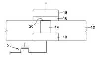
도 2는 종래의 상전이 메모리 소자의 구조를 보여주는 개략적인 단면도이다.2 is a schematic cross-sectional view illustrating a structure of a conventional phase change memory device.
도 3은 본 발명에 따른 상전이 메모리 소자의 구조를 보여주는 개략적인 단면도이다.3 is a schematic cross-sectional view illustrating a structure of a phase change memory device according to the present invention.
도 4는 본 발명에 따른 상전이 메모리 소자에서의 리셋전류의 예측치를 보여주는 그래프이다.4 is a graph showing an estimate of reset current in a phase change memory device according to the present invention.
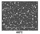
도 5a 내지 도 5e는 실시예2에서 각각 100℃, 200℃, 300℃, 400℃ 및 500℃의 온도에서 열처리된 상전이 나노입자들의 SEM 사진을 보여준다.5A to 5E show SEM images of phase-transfer nanoparticles heat-treated at temperatures of 100 ° C., 200 ° C., 300 ° C., 400 ° C. and 500 ° C. in Example 2, respectively.
도 6a 및 도 6b는 각각 EDX 분석용 Ge2Sb2Te5 나노입자의 SEM 사진과 상기 나노입자의 EDX 분석결과 그래프이다.6A and 6B are SEM pictures of Ge2 Sb2 Te5 nanoparticles for EDX analysis and EDX analysis graphs of the nanoparticles, respectively.
도 7은 열처리 온도에 따른 Ge2Sb2Te5 나노입자의 화학조성비 변화를 보여주는 그래프이다.7 is a graph showing the change in chemical composition ratio of Ge2 Sb2 Te5 nanoparticles according to the heat treatment temperature.
도 8a 내지 도 8c는 본 발명에 따른 상전이 메모리 소자의 제조방법을 보여주는 공정흐름도이다.8A through 8C are flowcharts illustrating a method of manufacturing a phase change memory device according to the present invention.
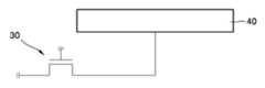
도 9는 I-V(current-voltage) 특성의 측정을 위해 실험예1에서 제조된 본 발명에 따른 상전이 메모리 소자의 개략적 단면도이다.9 is a schematic cross-sectional view of a phase change memory device according to the present invention manufactured in Experimental Example 1 for the measurement of current-voltage (I-V) characteristics.
도 10은 도 9의 상전이 메모리 소자를 리셋시키기 위하여 실제로 이용한 전압과 전류펄스의 모양을 보여주는 그래프이다.FIG. 10 is a graph showing shapes of voltage and current pulses actually used to reset the phase change memory device of FIG. 9.
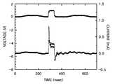
도 11은 도 9의 상전이 메모리 소자의 I-V(current-voltage) 특성을 측정한 결과그래프이다.FIG. 11 is a graph illustrating results of measuring current-voltage (I-V) characteristics of the phase-transition memory device of FIG. 9.
< 도면의 주요부분에 대한 부호의 설명 ><Description of Symbols for Major Parts of Drawings>
30:트랜지스터 40:제 1 전극30: transistor 40: first electrode
46:상전이 물질층 48:제 2 전극46: phase change material layer 48: second electrode
본 발명은 상전이 메모리 소자 및 그 제조방법에 관한 것으로, 보다 상세하게는 전력소모가 작고, 전류-전압 특성이 향상된 상전이 메모리 소자 및 그 제조방법에 관한 것이다.BACKGROUND OF THE
반도체 메모리 소자들은 전원 공급이 중단되었을 때, 데이터의 보유 유무에 따라, 크게 휘발성 메모리 소자 및 비휘발성 메모리 소자로 나눌 수 있다. 휘발성 메모리 소자들의 대표적인 것은 DRAM 소자들 및 SRAM 소자들이며, 비휘발성 메모리 소자들의 대표적인 것은 플래쉬 메모리 소자들이다. 이와 같은 전형적인 메모리 소자들은 저장된 전하의 유무에 따라 논리 "0" 또는 논리 "1"을 나타낸다. 휘발성 메모리 소자인 DRAM은, 주기적인 리프레쉬 동작이 필요하기 때문에, 높은 전하 저장능력이 요구되며, 이로 인해 커패시터 전극의 표면적을 증가시키기 위해 많은 노력이 시도되고 있다. 하지만, 커패시터 전극의 표면적 증가는 디램 소자의 집적도 증가를 어렵게 한다. 한편, 통상적인 플래쉬 메모리 셀들은 반도체 기판에 차례로 적층된 게이트 절연막, 부유게이트, 유전체막 및 제어게이트로 구성된 게이트 패턴을 갖는다. 플래쉬 메모리 셀에 데이터를 기록 또는 소거하는 원리는 상기 게이트 절연막을 통하여 전하들을 터널링 시키는 방법을 사용한다. 이 때, 전원전압에 비하여 높은 동작전압이 요구된다. 이로 인하여, 상기 플래쉬 메모리 소자들은 기록동작 및 소거동작에 필요한 전압을 형성하기 위하여 승압회로가 요구된다.When the power supply is interrupted, the semiconductor memory devices may be classified into volatile memory devices and nonvolatile memory devices according to whether data is retained. Representative of volatile memory devices are DRAM devices and SRAM devices, and representative of nonvolatile memory devices are flash memory devices. Such typical memory elements represent logic "0" or logic "1" depending on the presence or absence of stored charge. Since DRAM, which is a volatile memory device, requires periodic refresh operation, high charge storage capability is required, and thus, many efforts have been made to increase the surface area of a capacitor electrode. However, increasing the surface area of the capacitor electrode makes it difficult to increase the integration of the DRAM device. On the other hand, conventional flash memory cells have a gate pattern composed of a gate insulating film, a floating gate, a dielectric film, and a control gate sequentially stacked on a semiconductor substrate. The principle of writing or erasing data into a flash memory cell uses a method of tunneling charges through the gate insulating film. At this time, a higher operating voltage is required than the power supply voltage. As a result, the flash memory devices require a boosting circuit to form voltages necessary for writing and erasing operations.
따라서, 비휘발성 특성 및 임의 접근이 가능하고, 소자의 집적도도 증가시키면서 구조가 간단한 새로운 메모리 소자를 개발하기 위한 많은 노력이 있었으며, 이에 따라 나타난 대표적인 것이 상전이 메모리 소자이다. 상전이 메모리 소자는 상전이 물질을 이용한다. 상전이 물질에 제공되는 전류의 크기(즉, 주울 열)에 따라서, 상전이 물질은 비정질 상태 또는 결정질 상태에 있게 되며, 각각의 상태에서 전기전도도의 차이를 가진다.Therefore, many efforts have been made to develop a new memory device having a non-volatile characteristic and random access, and having a simple structure while increasing the integration of the device. A representative example of the phase change memory device is a phase change memory device. The phase change memory device uses a phase change material. Depending on the magnitude of the current (ie joule heat) provided to the phase change material, the phase change material is in an amorphous state or a crystalline state, and has a difference in electrical conductivity in each state.
도 1은 상전이 메모리 소자의 동작 방법을 보여주는 그래프이다. 상기 그래프에서, 상전이 메모리 셀에 데이터를 기억 및 소거시키는 방법이 설명될 수 있다. 여기서, 가로축은 시간(T)을 나타내고, 세로축은 상전이 물질막에 가해지는 온도 (Temperature; 단위℃)를 나타낸다.1 is a graph illustrating a method of operating a phase change memory device. In the above graph, a method of storing and erasing data in a phase change memory cell can be described. Here, the horizontal axis represents time T, and the vertical axis represents temperature (Unit C) applied to the phase change material film.
도 1을 참조하면, 상전이 물질막을 용융온도(melting temperture; Tm) 보다 높은 온도에서 짧은 시간(T1) 동안 가열한 후에, 빠른 속도로 냉각(quenching)시키면, 상전이 물질막은 비정질 상태(amorphous state)로 변한다(제1곡선). 이에 반하여, 상전이 물질막을 용융온도(Tm) 보다 낮고 결정화 온도(crystallization temperture; Tc) 보다 높은 온도에서 T1시간 보다 긴 T2시간 동안 가열(annealing)한 후에 서서히 냉각시키면, 상전이 물질막은 결정 상태(crystalline state)로 변한다(제2곡선). 비정질 상태를 갖는 상전이 물질막의 비저항은 결정질 상태를 갖는 상전이 물질막의 비저항 보다 높다. 따라서, 읽기 모드에서 상기 상변화 물질막을 통하여 흐르는 전류를 감지(detection)함으로써, 상기 상전이 메모리 셀에 저장된 정보가 논리 "1"인지 또는 논리 "0"인지를 판별(discriminate) 할 수 있다. 상기 상전이 물질막으로는 칼코게나이드 물질이 널리 사용된다. 칼코게나이드 물질 중에서 상전이 메모리에서 널리 사용하는 물질은 게르마늄(Ge), 안티몬(Sb) 및 텔루리움(Te)을 함유하는 화합물막(compound material layer; 이하 'GST막'이라 함)이다.Referring to FIG. 1, when the phase change material film is heated at a temperature higher than the melting temperature Tm for a short time T1 , and then rapidly cooled, the phase change material film is in an amorphous state. (First curve). In contrast, if the phase change material film is slowly cooled after annealing at a temperature lower than the melting temperature (Tm ) and higher than the crystallization temperature (Tc ) for T2 hours longer than T1 hour, the phase change material film is crystallized. Change to a crystalline state (second curve). The resistivity of the phase change material film having an amorphous state is higher than that of the phase change material film having a crystalline state. Accordingly, by detecting a current flowing through the phase change material layer in a read mode, it is possible to discriminate whether the information stored in the phase change memory cell is a logic "1" or a logic "0". Chalcogenide materials are widely used as the phase change material film. Among chalcogenide materials, a material widely used in phase change memory is a compound material layer containing germanium (Ge), antimony (Sb), and tellurium (Te) (hereinafter, referred to as a 'GST film').
도 2는 종래의 상전이 메모리 소자의 구조를 보여주는 개략적인 단면도이다.2 is a schematic cross-sectional view illustrating a structure of a conventional phase change memory device.
도 2를 참조하면, 종래의 상전이 메모리 소자는 하부 도전막(10)과 상부 도전막(18), 상기 두 도전막(10, 18) 사이에 개재되는 박막 형태의 상전이 물질막(16) 및 상기 하부 도전막(10)과 상전이 물질막(16)을 전기적으로 연결하는 콘택부(14)를 포함한다. 상기 하부 도전막(10) 및 콘택부(14)의 측면은 절연막(12)내에 매립되어 있으며, 상기 콘택부(14)의 접촉면(20)과 상기 상전이 물질막(16)이 전기적으로 연결된다. 또한, 상기 하부 도전막(10)에는 트랜지스터(5)가 전기적으로 연결되어 있으며, 상기 트랜지스터(5)를 통하여 상기 상하부 도전막(10, 18) 및 그 사이에 개재되는 상전이 물질막(16)에 전류가 유입되거나, 상부 도전막(18)을 통하여 유입된 전류가 상전이 물질막(16), 콘택부(14), 하부 도전막(10), 및 트랜지스터(5)를 거쳐 흐를 수 있다.Referring to FIG. 2, a conventional phase change memory device includes a lower
이와 같은 상전이 메모리 소자에서, 상기 하부 도전막(10) 및 상부 도전막 (18) 사이에 전류가 흐르면, 상기 콘택부(14)와 접촉면(20)을 통하여 상기 상전이 물질막(16)에 전류가 유입되며, 전류에 의한 주울열에 따라, 상기 접촉면(20) 주위의 상전이 물질의 결정 상태가 변한다. 상전이 물질의 결정 상태를 변화시키기 위해서 필요한 전류의 세기는 상기 접촉면(20)의 면적이 작을수록 작아진다. 그러나, 종래 박막 형태의 상전이 물질막(16)을 구비하는 상변화 메모리 소자에서, 상기 접촉면(20)의 면적을 줄이는 상변화 메모리 소자의 구조에는 한계가 있었으며, 보다 작은 전류밀도로 상기 상전이 물질의 결정 상태를 변화시키기 위하여 개선된 상변화 메모리 소자의 구조의 개발이 요구되었다.In the phase change memory device as described above, when a current flows between the lower
본 발명이 이루고자 하는 기술적 과제는 상술한 종래 기술의 문제점을 개선하기 위한 것으로서, 전력소모가 작고, 전류-전압 특성이 향상된 상전이 메모리 소자 및 그 제조방법을 제공함에 있다.SUMMARY OF THE INVENTION The present invention has been made in an effort to improve the above-described problems of the prior art, and to provide a phase change memory device having low power consumption and improved current-voltage characteristics, and a method of manufacturing the same.
본 발명에 따르면,According to the invention,
상호 대향 배치되는 제 1 전극 및 제 2 전극;A first electrode and a second electrode disposed to face each other;
상기 제 1 전극과 제 2 전극 사이에 개재되는 것으로 상전이 나노입자들을 포함하는 상전이 물질층; 및A phase change material layer interposed between the first electrode and the second electrode and including phase change nanoparticles; And
상기 제 1 전극에 전기적으로 연결되는 트랜지스터;를 구비하는 상전이 메모리 소자가 제공된다.A phase change memory device including a transistor electrically connected to the first electrode is provided.
여기에서, 상기 상전이 나노입자는 S, Se, Te, As, Sb, Ge, Sn, Ga, In 및 Ag으로 이루어지는 그룹에서 선택되는 하나 이상의 물질을 포함하는 화합물이며, 상기 나노입자의 직경은 1 내지 100nm의 범위에 있다. 바람직하게, 상기 상전이 메모리 소자는 상기 나노입자들 사이의 공극에 소정물질이 더 채워진 구조를 가진다. 상기 소정물질은 절연물질, 예를 들어 SiO2 또는 Si3N4 이다Here, the phase transition nanoparticles are compounds comprising at least one material selected from the group consisting of S, Se, Te, As, Sb, Ge, Sn, Ga, In and Ag, the diameter of the nanoparticles is 1 to It is in the range of 100 nm. Preferably, the phase change memory device has a structure in which a predetermined material is further filled in the pores between the nanoparticles. The predetermined material is an insulating material, for example SiO2 or Si3 N4 .
또한 본 발명에 따르면,Also according to the invention,
트랜지스터를 준비하는 단계;Preparing a transistor;
상기 트랜지스터에 전기적으로 연결되는 제 1 전극을 준비하는 단계;Preparing a first electrode electrically connected to the transistor;
상기 제 1 전극 상에 상전이 나노입자들을 포함하는 상전이 물질층을 형성하는 단계; 및Forming a phase change material layer including phase change nanoparticles on the first electrode; And
상기 상전이 물질층 상에 제 2 전극을 준비하는 단계;를 포함하는 상전이 메모리 소자의 제조방법이 제공된다.A method of manufacturing a phase change memory device is provided, including: preparing a second electrode on the phase change material layer.
여기에서, 상기 상전이 나노입자는 S, Se, Te, As, Sb, Ge, Sn, Ga, In 및 Ag으로 이루어지는 그룹에서 선택되는 하나 이상의 물질을 포함하는 화합물이며, 상기 나노입자의 직경은 1 내지 100nm의 범위에 있다.Here, the phase transition nanoparticles are compounds comprising at least one material selected from the group consisting of S, Se, Te, As, Sb, Ge, Sn, Ga, In and Ag, the diameter of the nanoparticles is 1 to It is in the range of 100 nm.
바람직하게, 상기 제 1 전극 상에 상전이 나노입자들을 포함하는 상전이 물질층을 형성하는 단계;는Preferably, forming a phase change material layer including phase change nanoparticles on the first electrode;
상전이 나노입자들을 준비하는 단계; 및Preparing phase transition nanoparticles; And
상기 제 1 전극 상에 상기 상전이 나노입자들을 포함하는 상전이 물질층을 형성하는 단계;를 포함한다.And forming a phase change material layer including the phase change nanoparticles on the first electrode.
상기 상전이 나노입자들은 레이저 어블레이션, 스퍼터링, 화학적 기상 증착, 침전 및 일렉트로 스프레이 등의 방법 중 하나의 방법으로 제조될 수도 있으며 바람직하게는 레이저 어블레이션 방법을 통해 제조하는 것이 좋다.The phase change nanoparticles may be prepared by one of methods such as laser ablation, sputtering, chemical vapor deposition, precipitation, and electrospray, and preferably, the method may be prepared by laser ablation.
상기 나노입자들을 준비하는 단계 후에 나노입자의 크기를 크고 균일하게 만들기 위해서 준비된 나노입자에 열처리를 추가로 할 수 있다. 바람직한 열처리 온도는 약 100~650℃이다. 100℃이하에서는 열처리의 효과가 없으며 650℃이상의 온도에서는 형성된 상전이 나노파티클이 녹게 되므로 바람직하지 않다. 또한 보다 바람직한 열처리 온도는 200~300℃이다.After preparing the nanoparticles, heat treatment may be further performed on the prepared nanoparticles to make the nanoparticles large and uniform in size. Preferable heat treatment temperature is about 100-650 degreeC. It is not preferable because the effect of heat treatment is less than 100 ℃ and the phase change formed at a temperature of 650 ℃ or more because the nanoparticles are melted. Moreover, more preferable heat processing temperature is 200-300 degreeC.
이와 같이 준비된 상전이 나노입자들은 열영동 방법 혹은 전기영동 방법 등을 통해서 상기 제1 전극상에 증착될 수 있으며, 상기 상전이 나노입자는 하나 이상의 층으로 증착될 수 있다.The phase change nanoparticles prepared as described above may be deposited on the first electrode through a thermophoretic method or an electrophoresis method, and the phase change nanoparticles may be deposited in one or more layers.
바람직하게는, 상기 제 1 전극 상에 상전이 나노입자들을 포함하는 상전이 물질층을 형성하는 단계;에서 상기 나노입자들 사이의 공극을 채우는 소정물질을 공급할 수 있으며 상기 소정물질로 절연물질을 사용할 수 있다. 절연물질로 사용되는 재료는 특별히 제한되지 않으며 SiO2 또는 Si3N4 등이 사용될 수 있다.Preferably, forming a phase change material layer including phase change nanoparticles on the first electrode; may supply a predetermined material to fill gaps between the nanoparticles and use an insulating material as the predetermined material. . The material used as the insulating material is not particularly limited and SiO2 or Si3 N4 may be used.
또한, 상기 상전이 물질층의 상전이 나노입자들의 물성을 조절하기 위해서 준비된 나노입자에 질소(nitrogen), 실리콘 등을 도핑처리 할 수 있다.In addition, the nanoparticles prepared for controlling the physical properties of the phase change nanoparticles of the phase change material layer may be doped with nitrogen (nitrogen), silicon, or the like.
이상과 같이 제조된 본 발명의 상전이 메모리 소자는 도 3에 도시된 바와 같다. 도 3을 참조하면, 본 발명에 따른 상전이 메모리 소자는 상호 대향 배치되는 제 1 전극(40) 및 제 2 전극(48), 상기 두 전극(40, 48) 사이에 개재되는 상전이 물질층(46) 및 상기 제 1 전극(40)에 전기적으로 연결되는 트랜지스터(30)을 구비한다. 여기에서, 상기 제 1 전극(40) 및 제 2 전극(48)은 도전체 재료로 형성된 것이다. 여기에서, 상기 제 1 전극(40)은 그 위에 작은 콘택사이즈를 가지는 저항성 히터(resistive heater)(미도시)를 더 포함할 수 있으며, 이러한 상전이 메모리 소자의 전극구조는 이미 공지된 기술이므로 이에 대한 상세한 설명은 생략하기로 한다.The phase change memory device of the present invention manufactured as described above is as shown in FIG. 3. Referring to FIG. 3, the phase change memory device according to the present invention may include a
본 발명에 따른 상전이 메모리 소자에서, 상기 트랜지스터(30) 또는 제 1 전극(40)을 통하여 상기 상전이 메모리 소자에 전류가 유입되어 상기 제 1 전극(40) 및 제 2 전극(48) 사이에 전류가 흐르면, 전류의 세기의 차이(즉, 주울 열)에 따라, 상기 제 1 전극(40) 및 제 2 전극(48) 사이에 개재된 상전이 물질층(46)의 결정 상태가 변한다. 구체적으로 설명하면, 상전이 물질층(46)에 제공되는 전류의 크기정도와 전류를 흘려주는 시간에 따라서, 상전이 물질층(46)은 비정 질 상태 또는 결정질 상태에 있게 되며, 각각의 상태에서 전기전도도의 차이가 생긴다. 비정질 상태를 갖는 상전이 물질층(46)의 비저항은 결정질 상태를 갖는 상전이 물질층(46)의 비저항 보다 높다. 따라서, 읽기 모드에서 상기 상변화 물질층(46)을 통하여 흐르는 전류를 감지(detection)함으로써, 상기 상전이 메모리 소자에 저장된 정보가 논리 "1"인지 또는 논리 "0"인지를 판별(discriminate) 할 수 있다.In the phase change memory device according to the present invention, a current flows into the phase change memory device through the
본 발명에서, 상기 상전이 물질층(46)은 상전이 나노입자들을 포함하여 형성되며, 이와 같은 본 발명의 특징은 종래 상전이 메모리 소자에서 박막 형태의 상전이 물질막이 채택되었던 것과 비교될 수 있다. 상전이 물질층(46)이 상전이 나노입자들을 포함하여 형성될 경우, 결정상에서 비정질상으로의 상전이에 필요한 전류(Ireset)의 크기는 종래 박막 형태의 상전이 물질의 상전이에 필요한 전류(Ireset)의 크기에 비해 작으며, 이를 도 4에 나타내었다.In the present invention, the phase
도 4는 본 발명에 따른 상전이 메모리 소자에서의 리셋전류의 예측치를 보여주는 그래프이다. 여기에서, 종래 박막형태의 상전이 물질막을 구비한 상전이 메모리 소자의 리셋전류가 함께 비교되었다. 여기에서, 상기 상전이 물질층의 크기, 즉 폭과 두께는 각각 0.5㎛ 및 0.1㎛ 이었으며, 하부전극 및 상부전극의 폭은 각각 50nm 및 0.5㎛ 이었다. 상기 그래프에서 나타나듯이, 본 발명에 따른 상전이 메모리 소자에서 상전이 나노입자들을 포함하는 상전이 물질층의 상전이에 필요한 리셋전류(Ireset)는 수 ㎂로 종래 박막 형태의 상전이 물질막을 구비하는 상전이 메모리 소자의 상전이에 필요한 리셋전류(Ireset)인 0.5~2mA 보다 현저히 감소하였음을 알 수 있다.4 is a graph showing an estimate of reset current in a phase change memory device according to the present invention. Here, the reset currents of the phase change memory devices having the phase change material film in the conventional thin film form were compared together. Here, the size of the phase change material layer, that is, width and thickness were 0.5 μm and 0.1 μm, respectively, and the widths of the lower electrode and the upper electrode were 50 nm and 0.5 μm, respectively. As shown in the graph, the reset current (Ireset ) required for the phase transition of the phase change material layer including the phase change nanoparticles in the phase change memory device according to the present invention is several ㎂ of the phase change memory device including the phase change material film of the conventional thin film type. It can be seen that it is significantly reduced than 0.5 ~ 2mA, the reset current (Ireset ) required for the phase transition.
따라서, 본 발명에 따른 상전이 메모리 소자에서 소자의 동작전류 및 전력소모가 종래 박막 형태의 상전이 물질막을 구비하는 상전이 메모리 소자에서 보다 크게 감소한다. 또한, 상전이 물질층(46)이 상전이 나노입자들을 포함하여 형성됨으로써, 동작전류가 감소하여 보다 작은 크기의 트랜지스터의 채용이 가능하다.따라서,상전이 메모리 소자의 부피가 줄어들며, 상전이 메모리 소자의 고집적화가 기대될 수 있다. 또한, 상기 상전이 물질층(46)을 이루는 나노입자들의 크기 및 조성 제어가 용이하여, 상기 상전이 물질층(46)의 특성이 용이하게 제어될 수 있으며, 상기 나노입자들의 표면처리를 통하여 상기 상전이 물질층(46)의 새로운 특성이 기대될 수 있다.Accordingly, the operation current and power consumption of the device in the phase change memory device according to the present invention are significantly reduced in the phase change memory device having a phase change material film in the form of a conventional thin film. In addition, since the phase
이하, 본 발명의 실시예에 따른 상전이 메모리 소자의 제조방법을 첨부된 도면을 참조하여 상세하게 설명한다.Hereinafter, a method of manufacturing a phase change memory device according to an embodiment of the present invention will be described in detail with reference to the accompanying drawings.
실시예1: 상전이 나노입자의 제조Example 1 Preparation of Phase Transition Nanoparticles
상전이 물질층(46)의 상전이 나노입자는 레이저 어블레이션 방법을 이용하여 제조하였다. 보다 구체적으로는 193nm의 파장을 가지는 ArF 엑시머 레이저를 사용하였으며, 레이저 펄스의 주파수는 5Hz, 펄스의 폭은 30 나노초이다. Ge2SB2Te5 물질을 레이저 어블레이션의 타겟으로 사용하였다. 레이저 어블레이션은 아르곤 분위기에서 0.1~5 Torr의 압력에서 이루어졌으며, 레이저의 에너지 밀도는 평방센티미 터당 2~5J을 사용하여 평균 크기 10~30nm의 상전이 나노입자를 제조하였다.The phase change nanoparticles of the phase
실시예2: 열처리에 따른 상전이 나노입자들의 물성변화Example 2 Change of Physical Properties of Phase Transition Nanoparticles by Heat Treatment
실시예1의 방법으로 제조된 상전이 나노입자들을 100~650℃의 온도 범위에서 열처리 하였으며 그 결과를 도 5a 내지 도 5e에 나타내었다.Phase transfer nanoparticles prepared by the method of Example 1 were heat-treated at a temperature range of 100 ~ 650 ℃ and the results are shown in Figures 5a to 5e.
각각의 열처리 온도에 따라, 나노입자들의 물리적 또는 화학적 특성이 변화될 수 있으며, 이와 같은 나노입자들의 특성은 상전이 물질층(46)의 특성에 영향을 미칠 수 있다.Depending on the respective heat treatment temperatures, the physical or chemical properties of the nanoparticles may change, and such properties of the nanoparticles may affect the properties of the phase
도 6a 및 도 6b는 각각 EDX 분석용 Ge2Sb2Te5 나노입자의 SEM 사진과 상기 나노입자의 EDX 분석결과 그래프이다. 여기에서, 도 6a의 1영역은 EDX 분석영역이다.6A and 6B are SEM pictures of Ge2 Sb2 Te5 nanoparticles for EDX analysis and EDX analysis graphs of the nanoparticles, respectively. Here,
도 7은 열처리 온도에 따른 Ge2Sb2Te5 나노입자의 화학조성비 변화를 보여주는 그래프이다. 상기 도 7을 참조하면, 나노입자의 열처리 온도는 각각 100, 200, 및 300℃ 이었다. 여기에서, 각각의 열처리 온도에 따른 화학조성의 의존성(dependence of chemical composition)이 관찰되었다. 예를 들어, 100℃에서 Ge원자와 Sb원자들의 조성이 상대적으로 부족하였으나, 더 높은 열처리 온도에서 나노입자들의 화학조성이 화화양론화(stoichiometric)될 수 있었다. 특히, 200℃에서 나노입자들이 가장 화학양론적인 Ge2Sb2Te5상(phase)을 가지는 것으로 관찰되었다. 따라서, 200℃의 열처리 온도에서 가장 우수한 화학양론 및 결정상(crystalline)의 Ge2Sb2Te5 나노입자를 얻을 수 있다는 것을 알 수 있다.7 is a graph showing the change in chemical composition ratio of Ge2 Sb2 Te5 nanoparticles according to the heat treatment temperature. Referring to FIG. 7, the heat treatment temperatures of the nanoparticles were 100, 200, and 300 ° C., respectively. Here, the dependence of chemical composition with each heat treatment temperature was observed. For example, the composition of Ge and Sb atoms was relatively insufficient at 100 ° C., but the chemical composition of nanoparticles could be stoichiometric at higher heat treatment temperatures. In particular, it was observed that at 200 ° C. nanoparticles had the most stoichiometric Ge2 Sb2 Te5 phase. Therefore, it can be seen that the best stoichiometry and crystalline Ge2 Sb2 Te5 nanoparticles can be obtained at a heat treatment temperature of 200 ° C.
실시예3: 본 발명의 상전이 메모리 소자의 제조Example 3 Fabrication of Phase Shift Memory Device of the Present Invention
도 8a 내지 도 8c는 본 발명에 따른 상전이 메모리 소자의 제조방법을 보여주는 공정흐름도이다. 여기에서, 동일한 부재에 대해서는 동일한 참조번호를 그대로 사용하여 설명하기로 한다.8A through 8C are flowcharts illustrating a method of manufacturing a phase change memory device according to the present invention. Here, the same members will be described using the same reference numerals as they are.
도 8a 내지 도 8c를 참조하면, 먼저 트랜지스터(30) 및 상기 트랜지스터(30)에 전기적으로 연결되는 제 1 전극(40)을 준비한다. 여기에서, 상기 제 1 전극(40)은 그 위에 작은 콘택사이즈를 가지는 저항성 히터(resistive heater)(미도시)를 더 포함할 수 있으며, 이러한 상전이 메모리 소자의 전극구조는 이미 공지된 기술이므로 이에 대한 상세한 설명은 생략하기로 한다. 그 다음에 상기 실시예1 혹은 실시예2의 방법으로 상전이 나노입자를 준비한다. 그 다음에, 열영동 방법(기판과 열영동 장치 상부사이의 온도차 200℃)을 이용하여 상기 상전이 나노입자들을 제 1 전극(40) 위에 증착시켜 상전이 물질층(46)을 형성한다. 그리고나서, 상기 상전이 물질층(46) 위에 제 2 전극(48)을 형성한다. 여기에서, 상기 제 1 전극(40) 및 제 2 전극(48)은 도전체 재료로 형성된 것이다. 이와 같은 공정을 통하여, 본 발명에 따른 상전이 메모리 소자를 얻을 수 있다.8A to 8C, first, a
실험예1: 본 발명의 상전이 메모리 소자와 종래 상전이 메모리 소자의 효과비교Experimental Example 1: Comparison of Effects of Phase-Transfer Memory Device and Conventional Phase-Transition Memory Device
도 9는 I-V(current-voltage) 특성의 측정을 위해 실험예1에서 제조된 본 발명에 따른 상전이 메모리 소자의 개략적 단면도이다.9 is a schematic cross-sectional view of a phase change memory device according to the present invention manufactured in Experimental Example 1 for the measurement of current-voltage (I-V) characteristics.
먼저, 실시예1의 레이져 어블레이션 방법으로 상전이 나노입자를 제조하되 압력조건을 2Torr로 하고 레이저의 에너지 밀도는 평방센티미터당 2.5J을 사용하여 평균 크기 10nm의 상전이 나노입자를 제조하였고, 상기 제조된 나노입자를 200℃에서 열처리 하였다. 그 다음에, 실시예3의 방법으로 본 발명의 상전이 메모리 소자를 제조하였다. 구체적으로 설명하면, Si 기판 위에 상변화물질 (Ge2Sb2Te5) 나노입자를 50nm 정도의 두께로 증착하고, 그 위에 300마이크로미터의 직경을 가지는 Al 전극을 형성하였다. 상기 Al 전극과 Si 기판 사이에 전류를 흘리면서 상변화에 따른 I-V 특성을 관찰하였다.First, the phase transition nanoparticles were prepared by the laser ablation method of Example 1, but the pressure condition was 2 Torr, and the energy density of the laser was prepared using the phase density nanoparticles having an average size of 10 nm using 2.5J per square centimeter. Nanoparticles were heat treated at 200 ℃. Next, the phase change memory device of the present invention was produced by the method of Example 3. Specifically, a phase change material (Ge2 Sb2 Te5 ) nanoparticles were deposited on a Si substrate with a thickness of about 50 nm, and an Al electrode having a diameter of 300 micrometers was formed thereon. The IV characteristic of the phase change was observed while flowing a current between the Al electrode and the Si substrate.
도 10은 도 9의 상전이 메모리 소자를 리셋시키기 위하여 실제로 이용한 전압과 전류펄스의 모양을 보여주는 그래프이다. 여기서 리셋은 상변화물질을 결정상태(저항이 낮은 상태)에서 비정질상태(저항이 높은 상태)로 바꾸는 것을 말한다. 도 6은 50ns 동안 1V 크기의 전압 펄스를 가했을 때, 흐르는 전류의 모양을 측정한 것이다. 여기에서, 흐르는 전류의 크기는 평균 0.3mA, 최대 0.8mA 정도임을 알 수 있다. 종래 하부 전극의 크기가 50nm 정도인 64Mb PRAM에서 리셋에 필요한 전류가 0.5 ~ 1.5 mA 정도임을 감안하면, 본 발명에 따른 상전이 메모리 소자에 의할 경우 훨씬 넓은 면적의 전극에서 오히려 적은 전류로 리셋이 가능하다는 것을 알 수 있다.FIG. 10 is a graph showing shapes of voltage and current pulses actually used to reset the phase change memory device of FIG. 9. Here, reset refers to changing a phase change material from a crystalline state (low resistance state) to an amorphous state (high resistance state). Figure 6 measures the shape of the current flowing when a voltage pulse of 1V magnitude is applied for 50ns. Here, it can be seen that the magnitude of the current flowing is about 0.3 mA on average and about 0.8 mA at maximum. Considering that the current required for resetting is about 0.5 to 1.5 mA in a 64Mb PRAM having a size of about 50 nm in the conventional lower electrode, the phase change memory device according to the present invention enables reset to a relatively small current in an electrode of a much larger area. You can see that.
도 11은 도 9의 상전이 메모리 소자의 I-V(current-voltage) 특성을 측정한 결과그래프이다. 도 9의 상전이 메모리 소자에 도 10의 그래프에서 보여준 펄스를 가하여 리셋이 되면, 상전이 물질층은 저항이 높은 상태가 된다(그래프에서 Reset state로 표시). 저항이 높은 상태에서 전류를 점점 많이 흘리면, 온도가 높아지면 서 비정질상태에서 결정상태로 상변화가 일어난다(Set). Set이 된 상태에서 전류의 크기를 줄이면 낮은 저항을 가지면서 전류가 감소한다(그래프에서 Set state로 표시). 전류를 0으로 줄인 후, 다시 리셋펄스를 가하여 비정질 상태로 만들고 I-V 특성을 반복적으로 측정하였다. 상기 그래프에서 반복적으로 리셋-셋(Reset-Set)이 안정적으로 일어나는 것을 보여준다.FIG. 11 is a graph illustrating results of measuring current-voltage (I-V) characteristics of the phase-transition memory device of FIG. 9. When the phase transition memory device of FIG. 9 is reset by applying the pulse shown in the graph of FIG. 10, the phase change material layer is in a high resistance state (indicated by the Reset state in the graph). As the current flows more and more at high resistance, a phase change occurs from the amorphous state to the crystalline state as the temperature increases. Reducing the amount of current in the set state reduces the current with low resistance (indicated by the set state in the graph). After reducing the current to 0, the reset pulse was applied again to make the amorphous state and the I-V characteristics were repeatedly measured. The graph repeatedly shows that Reset-Set occurs stably.
본 발명에 따르면, 두 전극 사이에 상전이 나노입자들을 포함하는 상전이 물질층이 구비된 상전이 메모리 소자 및 그 제조방법이 제공된다. 상전이 나노입자들이 적층되어 형성된 상전이 물질층이 결정상에서 비정질상으로의 상전이에 필요한 전류(Ireset)의 크기는 종래 박막 형태의 상전이 물질의 상전이에 필요한 전류(Ireset)의 크기 보다 더 작다. 따라서, 본 발명에 따른 상전이 메모리 소자에서 소자의 동작전류 및 전력소모가 종래 박막 형태의 상전이 물질막을 구비하는 상전이 메모리 소자에서 보다 크게 감소한다.According to the present invention, a phase change memory device including a phase change material layer including phase change nanoparticles between two electrodes is provided, and a method of manufacturing the same. The size of the current Ireset required for the phase transition of the phase change material layer formed by stacking the phase change nanoparticles from the crystal phase to the amorphous phase is smaller than the size of the current Ireset required for the phase transition of the phase change material in the form of a conventional thin film. Accordingly, the operation current and power consumption of the device in the phase change memory device according to the present invention are significantly reduced in the phase change memory device having a phase change material film in the form of a conventional thin film.
또한, 상기 상전이 물질층을 이루는 상전이 나노입자들의 크기 및 조성 제어가 용이하여, 상기 상전이 물질층의 특성이 용이하게 제어될 수 있으며, 상기 나노입자들의 표면처리를 통하여 상기 상전이 물질층의 새로운 특성이 기대될 수 있다.In addition, it is easy to control the size and composition of the phase change nanoparticles constituting the phase change material layer, the properties of the phase change material layer can be easily controlled, the new characteristics of the phase change material layer through the surface treatment of the nanoparticles Can be expected
또한, 상기 상전이 메모리 소자의 상전이 물질층을 상전이 나노입자들로 형성함으로써, 동작전류가 감소하여 보다 작은 크기의 트랜지스터의 채용이 가능하다.따라서,부피를 줄여 소자의 고집적화를 기대할 수 있고, 재현성의 개선 에도 기여할 수 있다.In addition, by forming the phase-transfer material layer of the phase-transfer memory device with phase-transfer nanoparticles, the operating current is reduced, so that the adoption of transistors of smaller size is possible. Therefore, high integration of the device can be expected by reducing the volume and reproducibility. It can also contribute to improvement.
본 발명에 따른 상전이 메모리 소자 및 그 제조방법은 차세대 반도체 메모리 소자의 제조에 적용될 수 있다.The phase change memory device and a method of manufacturing the same according to the present invention can be applied to the manufacture of next-generation semiconductor memory devices.
이러한 본원 발명의 이해를 돕기 위하여 몇몇의 모범적인 실시예가 설명되고 첨부된 도면에 도시되었으나, 이러한 실시예들은 단지 넓은 발명을 예시하고 이를 제한하지 않는다는 점이 이해되어야 할 것이며, 그리고 본 발명은 도시되고 설명된 구조와 배열에 국한되지 않는다는 점이 이해되어야 할 것이며, 이는 다양한 다른 수정이 당 분야에서 통상의 지식을 가진 자에게 일어날 수 있기 때문이다.While some exemplary embodiments have been described and illustrated in the accompanying drawings in order to facilitate understanding of the present invention, it should be understood that these embodiments merely illustrate the broad invention and do not limit it, and the invention is illustrated and described. It is to be understood that the invention is not limited to structured arrangements and arrangements, as various other modifications may occur to those skilled in the art.
Claims (23)
Translated fromKoreanPriority Applications (5)
| Application Number | Priority Date | Filing Date | Title |
|---|---|---|---|
| JP2005348039AJP2006165553A (en) | 2004-12-02 | 2005-12-01 | Phase change memory device including phase change material layer including phase change nanoparticles and method of manufacturing the same |
| DE602005026094TDE602005026094D1 (en) | 2004-12-02 | 2005-12-01 | A phase change memory device having a phase change material layer of phase change nanoparticles |
| EP05257416AEP1667244B1 (en) | 2004-12-02 | 2005-12-01 | Method of fabricating phase change memory device having phase change material layer containing phase change nano particles |
| US11/291,976US20060121391A1 (en) | 2004-12-02 | 2005-12-02 | Phase change memory device having phase change material layer containing phase change nano particles and method of fabricating the same |
| US12/382,032US8049202B2 (en) | 2004-12-02 | 2009-03-06 | Phase change memory device having phase change material layer containing phase change nano particles |
Applications Claiming Priority (2)
| Application Number | Priority Date | Filing Date | Title |
|---|---|---|---|
| KR20040100358 | 2004-12-02 | ||
| KR1020040100358 | 2004-12-02 |
Publications (2)
| Publication Number | Publication Date |
|---|---|
| KR20060061745A KR20060061745A (en) | 2006-06-08 |
| KR100668334B1true KR100668334B1 (en) | 2007-01-12 |
Family
ID=36844900
Family Applications (1)
| Application Number | Title | Priority Date | Filing Date |
|---|---|---|---|
| KR1020050021340AExpired - LifetimeKR100668334B1 (en) | 2004-12-02 | 2005-03-15 | A phase change memory device having a phase change material layer including phase change nanoparticles and a method of manufacturing the same |
Country Status (3)
| Country | Link |
|---|---|
| KR (1) | KR100668334B1 (en) |
| CN (1) | CN1812118A (en) |
| DE (1) | DE602005026094D1 (en) |
Families Citing this family (12)
| Publication number | Priority date | Publication date | Assignee | Title |
|---|---|---|---|---|
| KR100919692B1 (en)* | 2006-04-27 | 2009-10-06 | 재단법인서울대학교산학협력재단 | Phase change memory cell and manufacturing method thereof |
| KR100810615B1 (en) | 2006-09-20 | 2008-03-06 | 삼성전자주식회사 | Phase-transition memory device with high-temperature phase-transition pattern and method of manufacturing the same |
| GB0801494D0 (en) | 2007-02-23 | 2008-03-05 | Univ Ind & Acad Collaboration | Nonvolatile memory electronic device using nanowire used as charge channel and nanoparticles used as charge trap and method for manufacturing the same |
| KR100850905B1 (en)* | 2007-02-23 | 2008-08-07 | 고려대학교 산학협력단 | Non-volatile memory electronic device of nano-wire nanoparticle heterojunction and manufacturing method thereof |
| EP2269201A1 (en)* | 2008-04-18 | 2011-01-05 | Nxp B.V. | Tunable capacitor and switch using mems with phase change material |
| KR101436924B1 (en)* | 2013-04-11 | 2014-09-03 | 한국과학기술연구원 | Ovonic threshold switch device having n-doped chalcogenide material and manufacture method thereof |
| CN103915566B (en)* | 2014-04-16 | 2017-05-03 | 绍兴文理学院 | Memory device based on phase change quantum dots and manufacturing method thereof |
| CN104241527B (en)* | 2014-09-30 | 2017-10-27 | 中国科学院上海微系统与信息技术研究所 | V Sb Te phase-change material systems for phase transition storage and preparation method thereof |
| CN110335941B (en)* | 2019-07-03 | 2023-08-18 | 芯盟科技有限公司 | Phase change memory structure and forming method thereof |
| CN112635664B (en)* | 2020-11-26 | 2023-08-25 | 宁波大学 | A kind of In2S3 doped Sb phase-change thin film material and preparation method thereof |
| WO2022151182A1 (en)* | 2021-01-14 | 2022-07-21 | Yangtze Advanced Memory Industrial Innovation Center Co., Ltd | Phase-change memory cell and method for fabricating the same |
| CN113885103B (en)* | 2021-09-26 | 2023-03-10 | 中国人民解放军国防科技大学 | A Novel Infrared Stealth Material, Preparation Method and Application |
- 2005
- 2005-03-15KRKR1020050021340Apatent/KR100668334B1/ennot_activeExpired - Lifetime
- 2005-12-01DEDE602005026094Tpatent/DE602005026094D1/enactiveActive
- 2005-12-02CNCNA2005101266304Apatent/CN1812118A/enactivePending
Also Published As
| Publication number | Publication date |
|---|---|
| DE602005026094D1 (en) | 2011-03-10 |
| CN1812118A (en) | 2006-08-02 |
| KR20060061745A (en) | 2006-06-08 |
Similar Documents
| Publication | Publication Date | Title |
|---|---|---|
| US11031435B2 (en) | Memory device containing ovonic threshold switch material thermal isolation and method of making the same | |
| US7893418B2 (en) | Phase change memory cell having interface structures with essentially equal thermal impedances and manufacturing methods | |
| US7964468B2 (en) | Multi-level memory cell having phase change element and asymmetrical thermal boundary | |
| US7507986B2 (en) | Thermal isolation for an active-sidewall phase change memory cell | |
| US7456421B2 (en) | Vertical side wall active pin structures in a phase change memory and manufacturing methods | |
| US7514367B2 (en) | Method for manufacturing a narrow structure on an integrated circuit | |
| US7919766B2 (en) | Method for making self aligning pillar memory cell device | |
| US7599216B2 (en) | Phase change memory devices and fabrication methods thereof | |
| JP2006165553A (en) | Phase change memory device including phase change material layer including phase change nanoparticles and method of manufacturing the same | |
| KR101058856B1 (en) | Memory element and memory device using same | |
| US8357920B2 (en) | Electronic component, and a method of manufacturing an electronic component | |
| US9276202B2 (en) | Phase-change storage unit containing TiSiN material layer and method for preparing the same | |
| US7449360B2 (en) | Phase change memory devices and fabrication methods thereof | |
| US20110007555A1 (en) | Resistance change element, semiconductor memory device, manufacturing method and driving method thereof | |
| KR100668334B1 (en) | A phase change memory device having a phase change material layer including phase change nanoparticles and a method of manufacturing the same | |
| WO2011030916A1 (en) | Phase change material and phase change memory element | |
| CN100378998C (en) | Memory element and storage device using the same | |
| US8049202B2 (en) | Phase change memory device having phase change material layer containing phase change nano particles | |
| KR100695166B1 (en) | Method for manufacturing a phase change memory device having a fullerene layer | |
| Gyanathan et al. | Phase-change random access memory with multilevel resistances implemented using a dual phase-change material stack |
Legal Events
| Date | Code | Title | Description |
|---|---|---|---|
| PA0109 | Patent application | Patent event code:PA01091R01D Comment text:Patent Application Patent event date:20050315 | |
| A201 | Request for examination | ||
| PA0201 | Request for examination | Patent event code:PA02012R01D Patent event date:20050523 Comment text:Request for Examination of Application Patent event code:PA02011R01I Patent event date:20050315 Comment text:Patent Application | |
| PG1501 | Laying open of application | ||
| E902 | Notification of reason for refusal | ||
| PE0902 | Notice of grounds for rejection | Comment text:Notification of reason for refusal Patent event date:20060630 Patent event code:PE09021S01D | |
| E701 | Decision to grant or registration of patent right | ||
| PE0701 | Decision of registration | Patent event code:PE07011S01D Comment text:Decision to Grant Registration Patent event date:20061130 | |
| GRNT | Written decision to grant | ||
| PR0701 | Registration of establishment | Comment text:Registration of Establishment Patent event date:20070108 Patent event code:PR07011E01D | |
| PR1002 | Payment of registration fee | Payment date:20070109 End annual number:3 Start annual number:1 | |
| PG1601 | Publication of registration | ||
| PR1001 | Payment of annual fee | Payment date:20091214 Start annual number:4 End annual number:4 | |
| PR1001 | Payment of annual fee | Payment date:20110103 Start annual number:5 End annual number:5 | |
| PR1001 | Payment of annual fee | Payment date:20111229 Start annual number:6 End annual number:6 | |
| FPAY | Annual fee payment | Payment date:20130102 Year of fee payment:7 | |
| PR1001 | Payment of annual fee | Payment date:20130102 Start annual number:7 End annual number:7 | |
| FPAY | Annual fee payment | Payment date:20140103 Year of fee payment:8 | |
| PR1001 | Payment of annual fee | Payment date:20140103 Start annual number:8 End annual number:8 | |
| FPAY | Annual fee payment | Payment date:20141231 Year of fee payment:9 | |
| PR1001 | Payment of annual fee | Payment date:20141231 Start annual number:9 End annual number:9 | |
| FPAY | Annual fee payment | Payment date:20160104 Year of fee payment:10 | |
| PR1001 | Payment of annual fee | Payment date:20160104 Start annual number:10 End annual number:10 | |
| FPAY | Annual fee payment | Payment date:20170102 Year of fee payment:11 | |
| PR1001 | Payment of annual fee | Payment date:20170102 Start annual number:11 End annual number:11 | |
| FPAY | Annual fee payment | Payment date:20191226 Year of fee payment:14 | |
| PR1001 | Payment of annual fee | Payment date:20191226 Start annual number:14 End annual number:14 | |
| PR1001 | Payment of annual fee | Payment date:20201230 Start annual number:15 End annual number:15 | |
| PR1001 | Payment of annual fee | Payment date:20211229 Start annual number:16 End annual number:16 | |
| PR1001 | Payment of annual fee | Payment date:20221221 Start annual number:17 End annual number:17 |