KR100666018B1 - Processing device and processing method - Google Patents
Processing device and processing methodDownload PDFInfo
- Publication number
- KR100666018B1 KR100666018B1KR1020027001692AKR20027001692AKR100666018B1KR 100666018 B1KR100666018 B1KR 100666018B1KR 1020027001692 AKR1020027001692 AKR 1020027001692AKR 20027001692 AKR20027001692 AKR 20027001692AKR 100666018 B1KR100666018 B1KR 100666018B1
- Authority
- KR
- South Korea
- Prior art keywords
- processing
- transmission window
- shielding plate
- heating
- oxide film
- Prior art date
- Legal status (The legal status is an assumption and is not a legal conclusion. Google has not performed a legal analysis and makes no representation as to the accuracy of the status listed.)
- Expired - Fee Related
Links
Images


Classifications
- H—ELECTRICITY
- H01—ELECTRIC ELEMENTS
- H01L—SEMICONDUCTOR DEVICES NOT COVERED BY CLASS H10
- H01L21/00—Processes or apparatus adapted for the manufacture or treatment of semiconductor or solid state devices or of parts thereof
- H01L21/02—Manufacture or treatment of semiconductor devices or of parts thereof
- H01L21/04—Manufacture or treatment of semiconductor devices or of parts thereof the devices having potential barriers, e.g. a PN junction, depletion layer or carrier concentration layer
- H01L21/18—Manufacture or treatment of semiconductor devices or of parts thereof the devices having potential barriers, e.g. a PN junction, depletion layer or carrier concentration layer the devices having semiconductor bodies comprising elements of Group IV of the Periodic Table or AIIIBV compounds with or without impurities, e.g. doping materials
- H01L21/30—Treatment of semiconductor bodies using processes or apparatus not provided for in groups H01L21/20 - H01L21/26
- H01L21/302—Treatment of semiconductor bodies using processes or apparatus not provided for in groups H01L21/20 - H01L21/26 to change their surface-physical characteristics or shape, e.g. etching, polishing, cutting
- H01L21/306—Chemical or electrical treatment, e.g. electrolytic etching
- H01L21/3065—Plasma etching; Reactive-ion etching
- H—ELECTRICITY
- H01—ELECTRIC ELEMENTS
- H01L—SEMICONDUCTOR DEVICES NOT COVERED BY CLASS H10
- H01L21/00—Processes or apparatus adapted for the manufacture or treatment of semiconductor or solid state devices or of parts thereof
- H01L21/02—Manufacture or treatment of semiconductor devices or of parts thereof
- H01L21/02041—Cleaning
- H01L21/02043—Cleaning before device manufacture, i.e. Begin-Of-Line process
- H01L21/02052—Wet cleaning only
- H—ELECTRICITY
- H01—ELECTRIC ELEMENTS
- H01J—ELECTRIC DISCHARGE TUBES OR DISCHARGE LAMPS
- H01J37/00—Discharge tubes with provision for introducing objects or material to be exposed to the discharge, e.g. for the purpose of examination or processing thereof
- H01J37/32—Gas-filled discharge tubes
- H01J37/32009—Arrangements for generation of plasma specially adapted for examination or treatment of objects, e.g. plasma sources
- H01J37/32192—Microwave generated discharge
- H—ELECTRICITY
- H01—ELECTRIC ELEMENTS
- H01L—SEMICONDUCTOR DEVICES NOT COVERED BY CLASS H10
- H01L21/00—Processes or apparatus adapted for the manufacture or treatment of semiconductor or solid state devices or of parts thereof
- H01L21/02—Manufacture or treatment of semiconductor devices or of parts thereof
- H01L21/02041—Cleaning
- H01L21/02057—Cleaning during device manufacture
- H01L21/0206—Cleaning during device manufacture during, before or after processing of insulating layers
- H01L21/02063—Cleaning during device manufacture during, before or after processing of insulating layers the processing being the formation of vias or contact holes
- H—ELECTRICITY
- H01—ELECTRIC ELEMENTS
- H01L—SEMICONDUCTOR DEVICES NOT COVERED BY CLASS H10
- H01L21/00—Processes or apparatus adapted for the manufacture or treatment of semiconductor or solid state devices or of parts thereof
- H01L21/02—Manufacture or treatment of semiconductor devices or of parts thereof
- H01L21/04—Manufacture or treatment of semiconductor devices or of parts thereof the devices having potential barriers, e.g. a PN junction, depletion layer or carrier concentration layer
- H01L21/18—Manufacture or treatment of semiconductor devices or of parts thereof the devices having potential barriers, e.g. a PN junction, depletion layer or carrier concentration layer the devices having semiconductor bodies comprising elements of Group IV of the Periodic Table or AIIIBV compounds with or without impurities, e.g. doping materials
- H01L21/30—Treatment of semiconductor bodies using processes or apparatus not provided for in groups H01L21/20 - H01L21/26
- H01L21/31—Treatment of semiconductor bodies using processes or apparatus not provided for in groups H01L21/20 - H01L21/26 to form insulating layers thereon, e.g. for masking or by using photolithographic techniques; After treatment of these layers; Selection of materials for these layers
- H01L21/3105—After-treatment
- H01L21/311—Etching the insulating layers by chemical or physical means
- H01L21/31105—Etching inorganic layers
- H01L21/31111—Etching inorganic layers by chemical means
- H—ELECTRICITY
- H01—ELECTRIC ELEMENTS
- H01L—SEMICONDUCTOR DEVICES NOT COVERED BY CLASS H10
- H01L21/00—Processes or apparatus adapted for the manufacture or treatment of semiconductor or solid state devices or of parts thereof
- H01L21/67—Apparatus specially adapted for handling semiconductor or electric solid state devices during manufacture or treatment thereof; Apparatus specially adapted for handling wafers during manufacture or treatment of semiconductor or electric solid state devices or components ; Apparatus not specifically provided for elsewhere
- H01L21/67005—Apparatus not specifically provided for elsewhere
- H01L21/67011—Apparatus for manufacture or treatment
- H01L21/67098—Apparatus for thermal treatment
- H01L21/67115—Apparatus for thermal treatment mainly by radiation
- H—ELECTRICITY
- H01—ELECTRIC ELEMENTS
- H01J—ELECTRIC DISCHARGE TUBES OR DISCHARGE LAMPS
- H01J2237/00—Discharge tubes exposing object to beam, e.g. for analysis treatment, etching, imaging
- H01J2237/20—Positioning, supporting, modifying or maintaining the physical state of objects being observed or treated
- H01J2237/2001—Maintaining constant desired temperature
Landscapes
- Engineering & Computer Science (AREA)
- Physics & Mathematics (AREA)
- Manufacturing & Machinery (AREA)
- Power Engineering (AREA)
- Microelectronics & Electronic Packaging (AREA)
- Computer Hardware Design (AREA)
- Condensed Matter Physics & Semiconductors (AREA)
- General Physics & Mathematics (AREA)
- Chemical & Material Sciences (AREA)
- Plasma & Fusion (AREA)
- Chemical Kinetics & Catalysis (AREA)
- General Chemical & Material Sciences (AREA)
- Inorganic Chemistry (AREA)
- Analytical Chemistry (AREA)
- Health & Medical Sciences (AREA)
- Toxicology (AREA)
- Drying Of Semiconductors (AREA)
- Cleaning Or Drying Semiconductors (AREA)
- Plasma Technology (AREA)
Abstract
Translated fromKoreanDescription
Translated fromKorean본 발명은 피처리체 표면에 형성된 산화막을 제거하는 처리 장치 및 처리 방법에 관한 것이다.The present invention relates to a treatment apparatus and a treatment method for removing an oxide film formed on a surface of a workpiece.
종래, 웨이퍼에 형성된 미세한 홀 내의 자연 산화막을 유효하게 제거하는 방법으로서는 예컨대, 다음과 같은 표면 처리 방법이 있다.Conventionally, as a method of effectively removing the natural oxide film in the fine holes formed in the wafer, for example, the following surface treatment method is available.
우선, N2 가스와 H2 가스의 혼합 가스를 플라즈마로 활성화하여 활성 가스종을 형성하고, 이 활성 가스종의 하강 기류에 NF3 가스를 첨가하여 NF3 가스를 활성화한다. 이 NF3 가스의 활성 가스종을 웨이퍼 표면의 자연 산화막과 반응시켜 생성막을 형성하고, 그 후 웨이퍼를 소정 온도로 가열함으로써 상기 생성막을 승화시켜 제거한다.First, a mixed gas of N2 gas and H2 gas is activated by plasma to form an active gas species, and NF3 gas is added to the falling air stream of the active gas species to activate the NF3 gas. The active gas species of the NF3 gas is reacted with a natural oxide film on the wafer surface to form a production film, and then the substrate is sublimed and removed by heating the wafer to a predetermined temperature.
이러한 방법에 사용되는 장치로서는, 내부에 웨이퍼를 수납하는 처리 용기와, NF3 가스의 활성 가스종을 생성하는 NF3 활성 가스종 생성 장치와, 웨이퍼를 가열하기 위해서 처리 용기의 외부에 설치된 가열 수단과, 이 가열 수단과 상기 피처리체 사이에 설치되어 가열 수단으로부터의 열 에너지를 투과시키는 투과창을 구비한 처리 장치가 알려져 있다. 그리고, 웨이퍼의 표면에 형성된 자연 산화막에, NF3 가스의 활성 가스종을 저온에서 반응시켜 생성막을 형성하고, 이 생성막을 가열 수단으로 소정 온도로 가열하여 승화시켜, 상기 자연 산화막을 제거하는 식으로 되어 있다.As the device used for this method, with the processing container for accommodating the wafer therein, NF3 active gas species generation device, and a heating means provided outside the process vessel to heat the wafer to generate an activated gas species of the NF3 gas And a processing apparatus provided between the heating means and the object to be treated and having a transmission window through which heat energy from the heating means is transmitted. Then, a natural oxide film formed on the surface of the wafer is reacted with an active gas species of NF3 gas at a low temperature to form a product film, and the product film is heated to a predetermined temperature by a heating means to sublimate to remove the natural oxide film. It is.
그러나, 상기 처리 장치에서는 피처리 웨이퍼의 가열 처리후에, 새로운 피처리 웨이퍼를 처리 용기에 도입하여 저온 처리를 하려고 하면, 전회의 가열 처리시의 열이 투과창에 축적되어 있어, 이 투과창으로부터의 열 방사에 의해서 웨이퍼가 가열되어 버린다. 이 때문에, 투과창이 소정 온도까지 냉각되는 것을 기다리지 않으면 안되어, 처리 능률이 현저히 저하된다고 하는 문제점이 있었다.However, in the above processing apparatus, when a new to-be-processed wafer is introduced into the processing container and subjected to low temperature treatment after the heat treatment of the wafer to be processed, the heat during the previous heat treatment is accumulated in the transmission window, The wafer is heated by the heat radiation. For this reason, it is necessary to wait for the transmission window to cool down to a predetermined temperature, and there is a problem that the processing efficiency is significantly reduced.
본 발명은 상기 과제를 해결하기 위해서 이루어진 것으로, 투과창에 잔존하고 있는 가열 처리시의 열에 의해서 피처리체의 온도가 상승하는 것을 방지하고, 이에 의해서, 연속적으로 피처리체를 처리할 수 있는 처리 장치 및 처리 방법을 제공하는 것을 목적으로 하고 있다.This invention is made | formed in order to solve the said subject, The processing apparatus which can prevent the temperature of a to-be-processed object to rise by the heat at the time of the heat process which remain | survives in a transmission window, and can process a to-be-processed object continuously by this, It aims at providing the processing method.
청구항 1에 기재한 발명은 피처리체의 표면에 형성된 산화막을 제거하기 위한 처리 장치로서, 피처리체를 수납하는 처리 용기와, 활성 가스종을 생성하는 활성 가스종 생성 장치와, 처리 용기의 외부에 설치되어 피처리체를 가열하는 가열 수단과, 이 가열 수단과 피처리체 사이의 처리 용기에 설치된 것으로, 처리 용기의 내외를 기밀하게 차폐하는 동시에 가열 수단으로부터의 가열용 에너지를 투과시키는 투과창과, 피처리체와 투과창 사이에 끼우고 빼낼 수 있게 설치된 차폐판을 구비하고, 차폐판을 닫힌 상태로 하여 투과창으로부터 피처리체로의 방사열을 차단한 상태에서, 피처리체의 표면에 형성된 산화막에 활성 가스종을 저온 상태에서 반응시켜 생성막을 형성하고, 그 후, 차폐판을 열린 상태로 하여, 가열 수단으로부터의 방사열을 투과창을 통해서 생성막에 가하고, 소정 온도로 가열하여 기화시켜, 생성막을 제거하는 것을 특징으로 한다.The invention as set forth in claim 1 is a processing apparatus for removing an oxide film formed on a surface of an object to be processed, comprising: a processing container accommodating a processing object, an active gas species generating device for generating active gas species, and an outer portion of the processing container; And heating means for heating the object, a permeation window provided in the processing container between the heating means and the object, which transparently shields the inside and outside of the processing container and transmits the energy for heating from the heating means; A shielding plate provided between the transmission window and interposed therebetween is provided, and the active gas species is stored at a low temperature in the oxide film formed on the surface of the object under the condition that the shielding plate is closed to block radiant heat from the transmission window to the object. Reaction is carried out in a state to form a production film, and then, the shielding plate is opened, and radiant heat from the heating means is transmitted to the transmission window. It is added to the production film through, and heated to a predetermined temperature to vaporize, characterized in that the production film is removed.
청구항 2에 기재한 발명은 피처리체의 표면에 형성된 산화막을 제거하기 위한 처리 장치로서, 활성 가스종을 생성하는 활성 가스종 생성 장치를 구비하며 피처리체의 표면에 형성된 산화막에, 활성 가스종을 저온 상태에서 반응시켜 생성막을 형성하는 제1 처리실과, 피처리체를 가열하는 가열 수단을 구비하며 이 가열 수단에 의해 피처리체의 표면에 형성된 생성막을 소정 온도로 가열하여 기화시켜, 생성막을 제거하는 제2 처리실과, 이들 제1 처리실과 제2 처리실 사이에서 피처리체를 반송하는 반송 수단을 구비한 것을 특징으로 한다.The invention as set forth in claim 2 is a processing apparatus for removing an oxide film formed on a surface of a target object, comprising an active gas species generating device for generating active gas species, wherein the active gas species is stored at a low temperature in the oxide film formed on the surface of the target object. A second process chamber having a first process chamber for reacting in a state to form a product film and a heating means for heating the object to be processed, wherein the product film formed on the surface of the object to be processed is heated and vaporized by a predetermined temperature to remove the product film. And a conveying means for conveying the object to be processed between the processing chamber and the first processing chamber and the second processing chamber.
청구항 3에 기재한 발명은 활성 가스종이 NF3 가스의 활성 가스종인 것을 특징으로 한다.The invention described in claim 3 is characterized in that the active gas species is an active gas species of NF3 gas.
청구항 4에 기재한 발명은 차폐판에는, 이 차폐판을 냉각하는 냉각 수단이 설치되는 것을 특징으로 한다.According to the invention described in claim 4, the shielding plate is provided with cooling means for cooling the shielding plate.
청구항 5에 기재한 발명은 반송 수단이, 제1 처리실과 제2 처리실에 접속되는 동시에 내부가 비반응성 분위기로 이루어진 반송실 내에 설치되는 것을 특징으로 한다.The invention described in claim 5 is characterized in that the conveying means is provided in a conveying chamber which is connected to the first processing chamber and the second processing chamber and whose interior is made of a non-reactive atmosphere.
청구항 6에 기재한 발명은 활성 가스종 생성 장치가, 플라즈마 형성부를 갖 는 플라즈마 형성관과, 이 플라즈마 형성관 내에 N2 가스와 H2 가스를 공급하는 플라즈마 가스 도입부와, 플라즈마 형성관 내에서 하강하여 흐르는 활성 가스종에 NF3 가스를 첨가하는 NF3 가스 공급부를 구비하고 있는 것을 특징으로 한다.According to the invention described in claim 6, the active gas species generating apparatus includes a plasma forming tube having a plasma forming unit, a plasma gas introducing unit supplying N2 gas and H2 gas into the plasma forming tube, and a lowering in the plasma forming tube. And an NF3 gas supply unit for adding NF3 gas to the activated gas species.
청구항 7에 기재한 발명은 플라즈마 형성부가, 마이크로파를 발생하는 마이크로파 발생원과, 발생한 마이크로파를 플라즈마 형성관 내로 도입하는 도파관으로 이루어지는 것을 특징으로 한다.The invention described in claim 7 is characterized in that the plasma forming unit includes a microwave generating source for generating microwaves and a waveguide for introducing the generated microwaves into the plasma forming tube.
청구항 8에 기재한 발명은 피처리체를 수납하는 처리 용기와, 이 처리 용기의 외부에 설치되어 피처리체를 가열하는 가열 수단과, 이 가열 수단과 피처리체 사이의 처리 용기에 설치된 투과창과, 피처리체와 투과창 사이에 끼우고 빼낼 수 있게 설치된 차폐판을 갖는 처리 장치를 이용하여, 피처리체의 표면에 형성된 산화막을 제거하기 위한 처리 방법으로서, 차폐판을 닫힌 상태로 하여 투과창으로부터 피처리체로의 방사열을 차단한 상태에서, 피처리체의 표면에 형성된 산화막에, 활성 가스종을 저온 상태에서 반응시켜 생성막을 형성하고, 그 후, 차폐판을 열린 상태로 하여, 가열 수단으로부터의 방사열을 투과창을 통해서 생성막에 가하고, 소정 온도로 가열하여 기화시켜, 생성막을 제거하는 것을 특징으로 한다.Invention as described in Claim 8 has a processing container which accommodates a to-be-processed object, the heating means provided in the exterior of this processing container, and the to-be-processed object, the permeation window provided in the process container between this heating means and a to-be-processed object, A treatment method for removing an oxide film formed on a surface of an object by using a processing device having a shielding plate installed between the and the transmission window so as to be able to be pulled out of the transmission window. In a state in which the radiant heat is blocked, an active gas species is reacted with the oxide film formed on the surface of the target object at a low temperature to form a product film. Then, the shielding plate is opened to release the radiant heat from the heating means. It is added to the production film through, and heated to a predetermined temperature to vaporize, characterized in that the production film is removed.
청구항 9에 기재한 발명은 피처리체의 표면에 형성된 산화막을 제거하는 처리 방법으로서, 제1 처리실에서, 피처리체의 표면에 형성된 산화막에 활성 가스종을 저온 상태에서 반응시켜 생성막을 형성하는 공정과, 생성막이 형성된 피처리체를 상기 제1 처리실에서 제2 처리실로 반송하는 공정과, 제2 처리실에서, 피처리체 의 표면에 형성된 생성막을 소정 온도로 가열하고 기화시켜, 생성막을 제거하는 공정을 갖는 것을 특징으로 한다.The invention as set forth in claim 9 is a treatment method for removing an oxide film formed on a surface of a target object, the process comprising: reacting an active gas species in a low temperature state with an oxide film formed on the surface of a target object in a first processing chamber to form a resultant film; And a step of conveying the object to be processed formed with the production film from the first processing chamber to the second processing chamber, and heating and vaporizing the production film formed on the surface of the object to a predetermined temperature in the second processing chamber to remove the production film. It is done.
도 1은 본 발명의 제1 실시예의 처리 장치를 도시하는 구성도이다.1 is a configuration diagram showing a processing apparatus of a first embodiment of the present invention.
도 2는 도 1에 도시하는 처리 장치의 가동 셔터를 나타내는 II-II 선을 따르는 개략 평면도이다.FIG. 2 is a schematic plan view along the line II-II of the movable shutter of the processing apparatus shown in FIG. 1. FIG.
도 3은 도 2에서 III-III 선을 따르는 개략 단면도이다.3 is a schematic cross-sectional view taken along the line III-III in FIG. 2.
도 4는 가동 셔터의 다른 예를 도시하는 개략 평면도이다.4 is a schematic plan view showing another example of the movable shutter.
도 5는 본 발명의 제2 실시예의 처리 장치를 도시하는 구성도이다.5 is a configuration diagram showing a processing apparatus of a second embodiment of the present invention.
이하, 본 발명에 따른 처리 장치를 실시하기 위한 최적의 형태를 도면을 참조하여 설명한다.EMBODIMENT OF THE INVENTION Hereinafter, the optimal form for implementing the processing apparatus which concerns on this invention is demonstrated with reference to drawings.
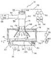
도 1 내지 도 3은 처리 장치의 제1 실시예를 도시하는 구성도이다. 도 1에서, 이 처리 장치(12)는 N2 가스와 H2 가스의 혼합 가스를 플라즈마로 활성화하는 플라즈마 형성관(14)과, 피처리체인 반도체 웨이퍼(W)에 대하여, 산화막, 특히 자연 산화막(대기 중의 산소나 세정액 등과의 접촉에 의해 의도하지 않게 형성된 산화막)을 제거하기 위한 소정의 표면 처리를 행하는 처리 용기(16)를 갖고 있다.1 to 3 are block diagrams showing the first embodiment of the processing apparatus. In Fig. 1, the
이 처리 용기(16)는 알루미늄에 의해 원통체형으로 성형되어 있고, 이 처리 용기(16) 내에는 상하 이동이 가능한 지지 부재(18)에 의해 지지된 석영제의 적재대(20)가 설치되어 있다. 처리 용기(16) 바닥부의 주연부에는 배기구(22)가 마련 되어, 처리 용기(16) 내를 진공 탈기 가능하게 하고 있다. 또, 적재대(20) 아래쪽의 처리 용기(16) 바닥부에는 조사구(26)가 형성되어 있고, 이 조사구(26)에는 석영제의 투과창(28)이 기밀하게 설치되어 있다. 이 투과창(28)의 아래쪽에는 상기 적재대(20)를 하면측에서 가열하기 위한 할로겐 램프 등으로 이루어지는 다수의 가열 램프(36)가 설치되어 있고, 이 가열 램프(36)로부터 방출되는 가열용의 광선이 투과창(28)을 투과하여 웨이퍼(W)의 이면에 입사하게 되어 있다.The
한편, 플라즈마 형성관(14)은 예컨대 석영에 의해 관상으로 성형되어 있고, 상기 처리 용기(16)의 천장부로 개구되는 동시에, 이 처리 용기(16)에 기립시킨 상태로 기밀하게 부착되어 있다. 이 플라즈마 형성관(14)의 상단에는 이 관 내에 N2 가스와 H2 가스로 이루어지는 플라즈마 가스를 도입하는 플라즈마 가스 도입부(44)가 마련된다. 이 플라즈마 도입부(44)는 플라즈마 형성관(14) 내에 삽입 관통된 도입 노즐(46)을 갖고 있고, 이 도입 노즐(46)에는 가스 통로(48)가 연결되어 있다. 이 가스 통로(48)에는 각각 매스플로우 컨트롤러와 같은 유량 제어기(50)를 통해, N2 가스가 충전된 N2 가스원(52) 및 H2 가스가 충전된 H2 가스원(54)이 접속되어 있다.On the other hand, the
또, 상기 도입 노즐(46)의 바로 아래에는 플라즈마 형성부(56)가 마련되어 있다. 이 플라즈마 형성부(56)는 2.45 GHz의 마이크로파를 발생하는 마이크로파 발생원(58)과, 상기 플라즈마 형성관(14)에 설치된 예컨대 에벤슨형의 도파관 등의 마이크로파 공급기(60)로 이루어져, 상기 마이크로파 발생원(58)에서 발생한 마이 크로파를 직사각형 도파관(62)을 통해 상기 마이크로파 공급기(60)에 공급하도록 되어 있다. 그리고, 이 공급된 마이크로파에 의해 플라즈마 형성관(14) 내에 플라즈마를 발생시켜, H2 가스와 N2 가스의 혼합 가스를 활성화하여, 이것의 하강 기류를 형성할 수 있게 되어 있다.In addition, a
상기 플라즈마 형성관(14)의 하단부인 유출구(64)에는 이것에 연통시켜, 아래 방향으로 우산형으로 넓어진 석영제의 덮개 부재(66)가 설치되어 있고, 적재대(20)의 윗쪽을 덮어 가스가 효율적으로 웨이퍼(W) 위로 흘러내리게 하도록 되어 있다. 그리고, 이 유출구(64)의 바로 아래에는 NF3 가스를 공급하기 위한 NF3 가스 공급부(68)가 설치된다. 이 NF3 가스 공급부(68)는 석영제의 링형의 샤워 헤드(70)를 지니고, 이 샤워 헤드(70)에는 다수의 가스 구멍(72)이 형성되어 있다. 이 샤워 헤드(70)는 연통관(74), 가스 통로(76), 유량 제어기(78)를 통해, NF3 가스가 충전된 NF3 가스원(80)에 접속되어 있다.The
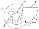
이러한 구성에 있어서, 적재대(20)와 투과창(28) 사이에는 가동 셔터(101)가 설치되어 있다. 이 가동 셔터(101)는 도 2 및 도 3에 도시한 바와 같은 것으로, 투과창(28)을 덮도록 회동 가능하게 배치된 차폐판(103)을 갖고 있고, 이 차폐판(103)에는 이 차폐판(103)을 회동시키는 회동축(105)이 설치되고, 이 회동축(105)은 처리 용기(16)의 외벽(107)을 관통하여 배치되어 있다. 이 회동축(105)과 외벽(107) 사이에는 이 회동축(105)과 외벽(107) 사이를 회동이 자유롭게 또한 기밀하게 유지하는 자성 유체 시일(109)이 설치되어 있다. 이 회동축(105)에는 축측 기어(111)가 설치되어 있고, 이 축측 기어(111)에는 모터측 기어(113)를 통해 구동 모터(115)가 설치되어 있다.In this configuration, the
그리고, 구동 모터(115)를 작동시킴으로써, 축측 기어(111)와 모터측 기어(113)를 통해 차폐판(103)을 회동시켜, 도 2에 도시하는 것과 같은 개방 위치와 도 3에 도시한 바와 같은 폐쇄 위치로 배치시킬 수 있게 되어 있다.Then, by operating the
또, 차폐판(103) 및 회동축(105)의 내부에는 냉매 통로(117)가 형성되어 있다. 이 냉매 통로(117)는 회동축(105)의 하단부에서 처리 용기(16)의 외부로 뻗어, 처리 용기(16) 외부에 마련된 냉매 순환 수단(119)에 접속되어 있다. 그리고, 이 냉매 순환 수단(119)에 의해서 냉매 통로(117)에 물 등의 냉매를 흘림으로써, 차폐판(103)을 냉각하도록 되어 있다. 이와 같이 함으로써, 투과창(28)으로부터의 복사열이 차폐판(103)에 도달하여 차폐판(103)의 온도가 상승하는 것을 방지할 수 있고, 따라서 차폐판(103)으로부터의 복사열이 웨이퍼(W)에 도달하여 웨이퍼의 온도가 상승하는 것을 방지할 수 있다.In addition, a
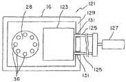
한편, 도 4는 다른 가동 셔터(121)의 예를 도시하는 도면이다. 이 가동 셔터(121)는 투과창(28)을 덮는 차폐판(123)을 갖고 있다. 이 차폐판(123)에는 2개의 구동축(125, 125)이 접속되어 있고, 이 구동축(125, 125)의 타단에는 유압 실린더(127)의 피스톤 로드가 연결되어 있다. 또한, 구동축(125)이 처리 용기(16)의 외벽(129)을 관통하는 부분에는 이 구동축(125)과 외벽(129) 사이에 자성 유체 시일(131)이 설치되어 있고, 구동축(125)과 외벽(129) 사이를 기밀하게 유지하면서 구동축을 외벽에 대하여 이동할 수 있게 되어 있다. 그리고, 유압 실린더(127)를 작동시킴으로써, 차폐판(123)을 개방 위치와 폐쇄 위치로 배치시킬 수 있게 되어 있다.4 is a figure which shows the example of the other
이 경우에도, 도 3에 도시하는 경우와 같이, 차폐판(123) 및 구동축(125) 내부에 냉매 통로를 형성하고, 처리 용기(16)의 외부에 위치하는 냉매 통로의 단부에, 처리 용기(16)의 외부에 설치한 냉매 순환 수단을 접속하여, 차폐판(123)을 냉각할 수 있게 구성할 수도 있다. 이와 같이 하면, 차폐판(123)으로부터의 복사열에 의한 웨이퍼(W)의 온도 상승을 억제할 수 있다.Also in this case, as shown in FIG. 3, a refrigerant passage is formed in the
다음에, 이상과 같이 구성된 장치를 이용하여 행해지는 자연 산화막의 제거 방법에 관해서 설명한다. 우선, 피처리체인 반도체 웨이퍼(W)를, 도시하지 않는 게이트 밸브를 통해 처리 용기(16) 내에 도입하여, 이것을 적재대(20) 위에 얹어 놓는다. 이 웨이퍼(W)에는 예컨대 전단계에서 컨택트홀 등이 형성되어 있고, 그 바닥부의 표면에 자연 산화막이 발생하고 있다.Next, the removal method of the natural oxide film performed using the apparatus comprised as mentioned above is demonstrated. First, the semiconductor wafer W which is an object to be processed is introduced into the
웨이퍼(W)를 처리 용기(16) 내에 반입했으면, 처리 용기(16) 내부를 밀폐하여, 내부를 진공 탈기한다. 그리고, N2 가스원(52) 및 H2 가스원(54)으로부터 N2 가스 및 H2 가스를 각각, 소정의 유량으로 플라즈마 가스 도입부(44)로부터 플라즈마 형성관(14) 내로 도입한다. 이와 동시에, 마이크로파 형성부(56)의 마이크로파 발생원(58)으로부터 2.45 GHz의 마이크로파를 발생하여, 이것을 마이크로파 공급기(60)로 유도하고, 이로부터 플라즈마 형성관(14) 내로 도입한다. 이에 따라, N2 가스와 H2 가스는 마이크로파에 의해 플라즈마화되는 동시에 활성화되어, 활 성 가스종이 형성된다. 이 활성 가스종은 처리 용기(16) 내의 진공 탈기에 의해 하강 기류를 형성하여 플라즈마 형성관(14) 속을 유출구(64)를 향해서 흘러 내리게 된다.When the wafer W is carried in the
한편, NF3 가스 공급부(68)의 링형의 샤워 헤드(70)로부터는 NF3 가스원(80)으로부터 공급된 NF3 가스가 N2 가스와 H2 가스로 이루어진 혼합 가스의 하강 기류의 활성 가스종에 첨가된다. 이 결과, 첨가된 NF3 가스도 하강 기류의 활성 가스종에 의해 활성화되게 된다. 이와 같이 NF3 가스도 활성 가스화되어, 상기한 하강 기류의 활성 가스종과 더불어 웨이퍼(W) 표면의 자연 산화막과 반응하여, Si, N, H, F가 혼합된 생성막을 형성하게 된다.On the other hand, NF3 from the ring-
이 처리는 저온에서 반응이 촉진되기 때문에, 이 처리 중에는 웨이퍼(W)는 가열되어서는 안되어, 실온 상태에서 생성막을 형성한다.Since this process accelerates the reaction at low temperatures, the wafer W should not be heated during this process to form the resulting film at room temperature.
여기서, 이 처리 중에는 가동 셔터(103)는 닫힌 상태로 되어 있다. 이것은 전회의 가열 처리 중에 가열된 투과창(28)으로부터의 복사열이 웨이퍼(W)에 도달하여, 웨이퍼의 온도가 상승하는 것을 방지하기 위해서이다.Here, the
이 때의 프로세스 조건은 가스의 유량에 관해서는 H2, NF3, N2이, 각각 10 sccm, 150 sccm, 1400 sccm이다. 프로세스 압력은 4 Torr, 플라즈마 전력은 400 W, 프로세스 시간은 1분이다. 이와 같은 식으로, 웨이퍼 표면에 자연 산화막과 반응한 생성막을 형성한다. 이 경우, 적재대(20)의 윗쪽은 우산형의 덮개 부재(66)에 의해 덮여져 있기 때문에 하강 기류의 활성 가스종의 분산이 억제되어, 이것이 효율적으로 웨이퍼면 위로 흘러 내려, 효율적으로 생성막을 형성할 수 있다.The process conditions at this time are 10 sccm, 150 sccm, and 1400 sccm of H2 , NF3 , and N2 with respect to the gas flow rate. The process pressure is 4 Torr, the plasma power is 400 W and the process time is 1 minute. In this manner, the resulting film reacted with the native oxide film is formed on the wafer surface. In this case, since the upper part of the mounting table 20 is covered by the umbrella cover member 66, the dispersion of active gas species in the downdraft is suppressed, and this flows down onto the wafer surface efficiently to efficiently form the resulting film. Can be formed.
이와 같이 생성막의 형성이 완료되면, H2, NF3, N2의 각각의 가스 공급을 정지하는 동시에, 마이크로파 발생원(58)의 구동도 정지하여, 처리 용기(16) 속을 진공 탈기하여 잔류 가스를 배제한다. 그 후, 가동 셔터(103)를 열린 상태로 배치시키고, 가열 램프(36)를 점등시켜 웨이퍼(W)를 소정의 온도, 예컨대 100℃ 이상으로 가열한다. 이 가열에 의해, 상기 생성막은 승화(기화)된다. 이에 따라, 웨이퍼(W)의 자연 산화막이 제거되어 웨이퍼 표면에 Si면이 나타나게 된다. 이 때의 프로세스 조건은 프로세스 압력이 1 mTorr 이하, 프로세스 시간은 2분 정도이다.When the formation of the production film is completed in this manner, the supply of gas to H2 , NF3 , and N2 is stopped, and the driving of the
이상 설명한 바와 같이, 이 처리 장치에서는 웨이퍼(W)와 투과창(28) 사이에 끼우고 빼낼 수 있는 가동 셔터(101)가 마련되어 있으므로, 활성화된 NF3 가스가 웨이퍼 표면의 자연 산화막과 반응하여, Si, N, H, F가 혼합된 생성막을 형성하는, 소위 저온 처리시에, 전회의 가열 처리시에 가열된 투과창(28)으로부터의 복사열에 의해 웨이퍼(W)가 가열되는 것을 방지할 수 있다. 이 때문에, 복수의 웨이퍼에 대해, 저온 처리와 가열 처리를 순차 반복 행하는 경우에, 저온 처리 중에 전회의 가열 처리에 의한 복사열에 의해 웨이퍼가 가열되어 버리는 것을 방지할 수 있다. 따라서, 저온 처리와 가열 처리를 연속적으로 간격을 두지 않고 할 수 있어, 산화막 제거 작업을 효율적으로 행할 수 있다.As described above, the processing apparatus is provided with a
또, 이 처리 장치의 가동 셔터에 있어서는 처리 용기 밖에 배치된 모터(115) 와 처리 용기 내의 차폐판(103)을 자성 유체 시일(109)에 의해 밀봉된 회전축(105)으로 연결하고 있으므로, 구동원을 처리 용기 내에 설치할 필요가 없고, 따라서 처리 용기를 소형으로 할 수 있는 동시에, 오염을 방지할 수 있다. 이러한 작용 효과는 도 4에 도시하는 왕복 운동형의 가동 셔터(121)에서도 마찬가지로 발휘된다.Moreover, in the movable shutter of this processing apparatus, since the
도 5는 본 발명의 제2 실시예를 도시하는 것이다. 이 처리 장치(201)는 저온 처리실과 가열 처리실을 따로 구비하는 것을 특징으로 한다. 이 처리 장치(201)는 중앙부에 반송실(203)을 갖고 있다. 이 반송실(203)에는 웨이퍼 반송용의 반송 장치가 설치된다. 이 반송실(203)의 내부는 비반응성 분위기, 예컨대 진공으로 이루어져 있고, 웨이퍼(W)의 반송 중에, 웨이퍼(W)에 자연 산화막이 발생하는 것을 억제할 수 있다. 이 반송실(203)에는 피처리 웨이퍼를 반송실(203) 내에 반입하기 위한 로드록실(205)이 마련되어 있다.5 shows a second embodiment of the present invention. This
한편, 상기 반송실(203)의 로드록실(205)과 반대측에는 2개의 저온 처리실(207, 207)이 각각 마련되어 있다. 이 저온 처리실(207)은 도 1에 도시하는 처리 장치(12)로부터 가동 셔터(101)와 가열 램프(36)를 없앤 것이다. 이 경우, 처리 용기(16)의 바닥부가 기밀하게 막힐 필요는 있지만, 처리 용기(16)의 바닥부를 막기 위한 부재가 도 1의 경우의 투과창(28)과 같이 광 투과성을 지닐 필요는 없다. 따라서, 도 1의 경우의 투과창(28) 대신에, 예컨대 알루미늄판으로 처리 용기(16)의 바닥부를 막는 식으로 하더라도 좋다. 이 저온 처리실(207)에서는 활성화된 NF3 가스가 웨이퍼 표면의 자연 산화막과 반응하여, Si, N, H, F가 혼합된 생성막을 형성한다.On the other hand, two low
또, 반송실(203)에는 가열실(209)이 마련되어 있다. 이 가열실(209)의 내부에는 가열 수단, 예컨대 공지된 저항 가열식 스테이지 히터가 설치되고, 이 스테이지 히터에 의해 웨이퍼(W)를 가열할 수 있다. 이 가열실(209)에서는 저온 처리후의 웨이퍼(W)를 소정의 온도, 예컨대 100℃ 이상으로 가열하여, 이 가열에 의해 상기 생성막은 승화(기화)한다. 이에 따라, 웨이퍼(W)의 자연 산화막이 제거된다.In addition, the
또, 반송실(203)에는 냉각실(211)이 마련되어 있다. 이 냉각실(211)은 가열 처리후의 웨이퍼를 냉각하기 위한 것이다. 처리후의 웨이퍼는 수지제의 카세트에 수납되어 반출되도록 되어 있지만, 웨이퍼가 고온 그대로라면 수지제 카세트를 상하게 할 우려가 있다. 이 때문에, 카세트에 수납하기 전에 웨이퍼를 냉각하도록 하고 있다.In addition, a
이러한 처리 장치(201)에서, 자연 산화막이 표면에 형성된 피처리 웨이퍼는 로드록실(205)로부터 반송실(203)로 반입된다. 이어서, 이 웨이퍼는 저온 처리실(207)에 반송되어, 여기에서 소위 저온 처리를 실시한다. 여기서, 이 처리 장치(201)에서는 저온 처리실(207)에 대응하여 가열실(209)이 별도로 설치되므로, 전회의 가열 처리중인 열이 잔존하여 저온 처리에 악영향을 미치게 하는 것을 방지할 수 있다. 그 후, 피처리 웨이퍼는 가열실(209)로 보내진다. 여기서, 저온 처리후의 웨이퍼(W)를 소정의 온도, 예컨대 100℃ 이상으로 가열하여, 이 가열에 의해 상기 생성막은 승화(기화)한다. 이에 따라, 웨이퍼(W)의 자연 산화막이 제거된다. 그 후, 이 가열된 웨이퍼는 냉각실(211)로 보내진다. 웨이퍼는 여기서 냉각되고 나서, 카세트에 수납되어 반출된다. 따라서, 고온 그대로의 웨이퍼가 수지제 카세트를 상하게 할 우려를 방지할 수 있다.In such a
이상 설명한 바와 같이, 이 처리 장치(201)에서는 저온 처리실(207)과 가열 처리실(209)이 각각 별도로 마련되므로, 활성화된 NF3 가스가 웨이퍼 표면의 자연 산화막과 반응하여, Si, N, H, F가 혼합한 생성막을 형성하는, 소위 저온 처리시에, 가열 처리의 영향에 의해서 웨이퍼가 가열되는 것을 방지할 수 있다. 따라서, 저온 처리와 가열 처리를 연속적으로 간격을 두지 않고서 할 수 있고, 따라서 산화막 제거 작업을 효율적으로 행할 수 있다.As described above, in the
본 발명에서는 피처리체와 투과창 사이에 끼우고 빼낼 수 있게 차폐판을 설치하고 있다. 따라서, 차폐판을 닫힌 상태로 하여 투과창으로부터의 방사열을 차단하여, 저온 상태에서 산화막에 활성 가스종을 반응시킬 수 있다. 또한, 본 발명에서는 산화막에 활성 가스종을 반응시키는 저온 처리와 그 후의 가열 처리를 별도의 실에서 실행하고 있다. 따라서, 저온 처리와 가열 처리를 연속해서 할 수 있어, 산화막 제거 작업을 효율적으로 행할 수 있다.In the present invention, a shielding plate is provided so as to be sandwiched between the workpiece and the transmission window. Therefore, the heat shield from the transmission window can be blocked by keeping the shielding plate closed, and the active gas species can be reacted with the oxide film in a low temperature state. In the present invention, the low temperature treatment and subsequent heating treatment for reacting the active gas species with the oxide film are carried out in separate chambers. Therefore, the low temperature treatment and the heat treatment can be performed continuously, and the oxide film removing operation can be efficiently performed.
Claims (12)
Translated fromKoreanApplications Claiming Priority (2)
| Application Number | Priority Date | Filing Date | Title |
|---|---|---|---|
| JPJP-P-1999-00229338 | 1999-08-13 | ||
| JP22933899AJP4057198B2 (en) | 1999-08-13 | 1999-08-13 | Processing apparatus and processing method |
Publications (2)
| Publication Number | Publication Date |
|---|---|
| KR20020027529A KR20020027529A (en) | 2002-04-13 |
| KR100666018B1true KR100666018B1 (en) | 2007-01-10 |
Family
ID=16890603
Family Applications (1)
| Application Number | Title | Priority Date | Filing Date |
|---|---|---|---|
| KR1020027001692AExpired - Fee RelatedKR100666018B1 (en) | 1999-08-13 | 2000-08-11 | Processing device and processing method |
Country Status (4)
| Country | Link |
|---|---|
| US (3) | US20050150455A1 (en) |
| JP (1) | JP4057198B2 (en) |
| KR (1) | KR100666018B1 (en) |
| WO (1) | WO2001013419A1 (en) |
Families Citing this family (19)
| Publication number | Priority date | Publication date | Assignee | Title |
|---|---|---|---|---|
| KR100338768B1 (en)* | 1999-10-25 | 2002-05-30 | 윤종용 | Method for removing oxide layer and semiconductor manufacture apparatus for removing oxide layer |
| US7604701B2 (en)* | 2003-07-14 | 2009-10-20 | Tokyo Electron Limited | Method and apparatus for removing external components from a process chamber without compromising process vacuum |
| JP2005093909A (en)* | 2003-09-19 | 2005-04-07 | Tokyo Electron Ltd | Substrate processing method and substrate processing apparatus |
| US20050230350A1 (en) | 2004-02-26 | 2005-10-20 | Applied Materials, Inc. | In-situ dry clean chamber for front end of line fabrication |
| US7780793B2 (en)* | 2004-02-26 | 2010-08-24 | Applied Materials, Inc. | Passivation layer formation by plasma clean process to reduce native oxide growth |
| JP2007012734A (en)* | 2005-06-29 | 2007-01-18 | Matsushita Electric Ind Co Ltd | Plasma etching apparatus and plasma etching method |
| KR100691137B1 (en)* | 2005-12-26 | 2007-03-12 | 동부일렉트로닉스 주식회사 | Manufacturing Method of Image Sensor |
| US7994002B2 (en) | 2008-11-24 | 2011-08-09 | Applied Materials, Inc. | Method and apparatus for trench and via profile modification |
| JP5274649B2 (en)* | 2009-03-26 | 2013-08-28 | 株式会社アルバック | Vacuum processing method and vacuum processing apparatus |
| US8617411B2 (en)* | 2011-07-20 | 2013-12-31 | Lam Research Corporation | Methods and apparatus for atomic layer etching |
| US9499905B2 (en)* | 2011-07-22 | 2016-11-22 | Applied Materials, Inc. | Methods and apparatus for the deposition of materials on a substrate |
| JP5507654B2 (en)* | 2012-11-30 | 2014-05-28 | ルネサスエレクトロニクス株式会社 | Manufacturing method of semiconductor device |
| US9879908B2 (en)* | 2013-10-17 | 2018-01-30 | Triglia Technologies, Inc. | System and method of removing moisture from fibrous or porous materials using microwave radiation and RF energy |
| CN103745924B (en)* | 2013-12-24 | 2016-08-17 | 中国电子科技集团公司第十六研究所 | A kind of preparation method of high-temperature superconductor Lange coupler |
| JP6230954B2 (en)* | 2014-05-09 | 2017-11-15 | 東京エレクトロン株式会社 | Etching method |
| US9793104B2 (en) | 2015-01-29 | 2017-10-17 | Aixtron Se | Preparing a semiconductor surface for epitaxial deposition |
| JP6356207B2 (en)* | 2016-12-15 | 2018-07-11 | 東京エレクトロン株式会社 | Substrate drying method and substrate processing apparatus |
| JP6325067B2 (en)* | 2016-12-15 | 2018-05-16 | 東京エレクトロン株式会社 | Substrate drying method and substrate processing apparatus |
| TWI616555B (en)* | 2017-01-17 | 2018-03-01 | 漢民科技股份有限公司 | Gas injectorused for semiconductor equipment |
Family Cites Families (66)
| Publication number | Priority date | Publication date | Assignee | Title |
|---|---|---|---|---|
| US3716424A (en)* | 1970-04-02 | 1973-02-13 | Us Navy | Method of preparation of lead sulfide pn junction diodes |
| US4192706A (en)* | 1975-01-22 | 1980-03-11 | Tokyo Shibaura Electric Co., Ltd. | Gas-etching device |
| US4123663A (en)* | 1975-01-22 | 1978-10-31 | Tokyo Shibaura Electric Co., Ltd. | Gas-etching device |
| US4391617A (en) | 1978-09-15 | 1983-07-05 | Way Peter F | Process for the recovery of vaporized sublimates from gas streams |
| US4572956A (en)* | 1982-08-31 | 1986-02-25 | Tokyo Shibaura Denki Kabushiki Kaisha | Electron beam pattern transfer system having an autofocusing mechanism |
| US4599869A (en)* | 1984-03-12 | 1986-07-15 | Ozin Geoffrey A | Cryogenic deposition of catalysts |
| KR920004171B1 (en)* | 1984-07-11 | 1992-05-30 | 가부시기가이샤 히다찌세이사꾸쇼 | Dry etching apparatus |
| JPH0766910B2 (en)* | 1984-07-26 | 1995-07-19 | 新技術事業団 | Semiconductor single crystal growth equipment |
| US4689112A (en)* | 1985-05-17 | 1987-08-25 | Emergent Technologies Corporation | Method and apparatus for dry processing of substrates |
| US4699689A (en)* | 1985-05-17 | 1987-10-13 | Emergent Technologies Corporation | Method and apparatus for dry processing of substrates |
| US4687544A (en)* | 1985-05-17 | 1987-08-18 | Emergent Technologies Corporation | Method and apparatus for dry processing of substrates |
| US4863561A (en)* | 1986-12-09 | 1989-09-05 | Texas Instruments Incorporated | Method and apparatus for cleaning integrated circuit wafers |
| US4913929A (en)* | 1987-04-21 | 1990-04-03 | The Board Of Trustees Of The Leland Stanford Junior University | Thermal/microwave remote plasma multiprocessing reactor and method of use |
| JPS6474717A (en) | 1987-09-17 | 1989-03-20 | Matsushita Electric Industrial Co Ltd | Formation of thin film |
| JP2637121B2 (en) | 1987-11-26 | 1997-08-06 | 株式会社東芝 | Photoexcitation reactor |
| US4952273A (en)* | 1988-09-21 | 1990-08-28 | Microscience, Inc. | Plasma generation in electron cyclotron resonance |
| US4952299A (en)* | 1988-10-31 | 1990-08-28 | Eaton Corporation | Wafer handling apparatus |
| US5030319A (en)* | 1988-12-27 | 1991-07-09 | Kabushiki Kaisha Toshiba | Method of oxide etching with condensed plasma reaction product |
| JP2981243B2 (en) | 1988-12-27 | 1999-11-22 | 株式会社東芝 | Surface treatment method |
| US5076205A (en)* | 1989-01-06 | 1991-12-31 | General Signal Corporation | Modular vapor processor system |
| US4988644A (en)* | 1989-05-23 | 1991-01-29 | Texas Instruments Incorporated | Method for etching semiconductor materials using a remote plasma generator |
| JPH03155621A (en) | 1989-07-12 | 1991-07-03 | Toshiba Corp | Dry etching method |
| US5028724A (en) | 1990-03-30 | 1991-07-02 | Air Products And Chemicals, Inc. | Synthesis of volatile fluorinated and non-fluorinated metal-beta-ketonate and metal-beta-ketoiminato complexes |
| JPH0432230A (en)* | 1990-05-29 | 1992-02-04 | Tokyo Electron Ltd | Dry washing device |
| US5041719A (en)* | 1990-06-01 | 1991-08-20 | General Electric Company | Two-zone electrical furnace for molecular beam epitaxial apparatus |
| US5223453A (en)* | 1991-03-19 | 1993-06-29 | The United States Of America As Represented By The United States Department Of Energy | Controlled metal-semiconductor sintering/alloying by one-directional reverse illumination |
| JP3084497B2 (en)* | 1992-03-25 | 2000-09-04 | 東京エレクトロン株式会社 | Method for etching SiO2 film |
| JP3148004B2 (en)* | 1992-07-06 | 2001-03-19 | 株式会社東芝 | Optical CVD apparatus and method for manufacturing semiconductor device using the same |
| US5282925A (en) | 1992-11-09 | 1994-02-01 | International Business Machines Corporation | Device and method for accurate etching and removal of thin film |
| US5516732A (en) | 1992-12-04 | 1996-05-14 | Sony Corporation | Wafer processing machine vacuum front end method and apparatus |
| DE69304038T2 (en)* | 1993-01-28 | 1996-12-19 | Applied Materials Inc | Device for a vacuum process with improved throughput |
| JP2804700B2 (en)* | 1993-03-31 | 1998-09-30 | 富士通株式会社 | Semiconductor device manufacturing apparatus and semiconductor device manufacturing method |
| US5501740A (en)* | 1993-06-04 | 1996-03-26 | Applied Science And Technology, Inc. | Microwave plasma reactor |
| JP3270196B2 (en)* | 1993-06-11 | 2002-04-02 | 川崎マイクロエレクトロニクス株式会社 | Thin film formation method |
| US5616206A (en)* | 1993-06-15 | 1997-04-01 | Ricoh Company, Ltd. | Method for arranging conductive particles on electrodes of substrate |
| JP2933469B2 (en) | 1993-07-12 | 1999-08-16 | 大日本スクリーン製造株式会社 | Heat treatment equipment |
| US5350480A (en)* | 1993-07-23 | 1994-09-27 | Aspect International, Inc. | Surface cleaning and conditioning using hot neutral gas beam array |
| US5616208A (en) | 1993-09-17 | 1997-04-01 | Tokyo Electron Limited | Vacuum processing apparatus, vacuum processing method, and method for cleaning the vacuum processing apparatus |
| TW277007B (en) | 1993-09-17 | 1996-06-01 | Tokyo Electron Co Ltd | |
| JPH08186081A (en) | 1994-12-29 | 1996-07-16 | F T L:Kk | Semiconductor device manufacturing method and semiconductor device manufacturing apparatus |
| JPH08193271A (en)* | 1995-01-13 | 1996-07-30 | Aneruba Kk | Preliminary treatment completion point detector after on-the-spot cleaning treatment and completion point detection |
| JP3553204B2 (en)* | 1995-04-28 | 2004-08-11 | アネルバ株式会社 | CVD equipment |
| US6002109A (en)* | 1995-07-10 | 1999-12-14 | Mattson Technology, Inc. | System and method for thermal processing of a semiconductor substrate |
| US5830272A (en)* | 1995-11-07 | 1998-11-03 | Sputtered Films, Inc. | System for and method of providing a controlled deposition on wafers |
| US5728260A (en)* | 1996-05-29 | 1998-03-17 | Applied Materials, Inc. | Low volume gas distribution assembly and method for a chemical downstream etch tool |
| US5802439A (en)* | 1997-02-19 | 1998-09-01 | Lockheed Martin Idaho Technologies Company | Method for the production of 99m Tc compositions from 99 Mo-containing materials |
| JP3627451B2 (en)* | 1997-06-04 | 2005-03-09 | 東京エレクトロン株式会社 | Surface treatment method and apparatus |
| US6706334B1 (en)* | 1997-06-04 | 2004-03-16 | Tokyo Electron Limited | Processing method and apparatus for removing oxide film |
| US5968279A (en)* | 1997-06-13 | 1999-10-19 | Mattson Technology, Inc. | Method of cleaning wafer substrates |
| JPH1154496A (en) | 1997-08-07 | 1999-02-26 | Tokyo Electron Ltd | Heat treatment system and gas processing system |
| US6352593B1 (en)* | 1997-08-11 | 2002-03-05 | Torrex Equipment Corp. | Mini-batch process chamber |
| US20030049372A1 (en)* | 1997-08-11 | 2003-03-13 | Cook Robert C. | High rate deposition at low pressures in a small batch reactor |
| US6006694A (en)* | 1997-12-05 | 1999-12-28 | Tegal Corporation | Plasma reactor with a deposition shield |
| FR2774460B1 (en)* | 1998-02-03 | 2000-03-24 | Elf Aquitaine | METHOD FOR MANAGING A THERMOCHEMICAL REACTION OR SOLID-GAS ADSORPTION |
| WO1999049101A1 (en)* | 1998-03-23 | 1999-09-30 | Mattson Technology, Inc. | Apparatus and method for cvd and thermal processing of semiconductor substrates |
| US6300600B1 (en)* | 1998-08-12 | 2001-10-09 | Silicon Valley Group, Inc. | Hot wall rapid thermal processor |
| JP2000124195A (en) | 1998-10-14 | 2000-04-28 | Tokyo Electron Ltd | Surface treatment method and device |
| JP3631063B2 (en)* | 1998-10-21 | 2005-03-23 | キヤノン株式会社 | Method for purifying fluoride and method for producing fluoride crystal |
| KR100605884B1 (en) | 1998-11-11 | 2006-08-01 | 동경 엘렉트론 주식회사 | Surface treatment method and surface treatment apparatus |
| JP4124543B2 (en)* | 1998-11-11 | 2008-07-23 | 東京エレクトロン株式会社 | Surface treatment method and apparatus |
| JP2000323487A (en)* | 1999-05-14 | 2000-11-24 | Tokyo Electron Ltd | Sheet-by-sheet type heat treatment device |
| US6849328B1 (en) | 1999-07-02 | 2005-02-01 | Ppg Industries Ohio, Inc. | Light-transmitting and/or coated article with removable protective coating and methods of making the same |
| JP2001110785A (en) | 1999-10-12 | 2001-04-20 | Tokyo Electron Ltd | Treatment method |
| EP1654473B1 (en) | 2003-08-06 | 2011-12-28 | Continental Teves AG & Co. oHG | Motor vehicle brake system |
| TWM277007U (en) | 2004-11-24 | 2005-10-01 | Chin-Feng Wu | Combination structure improvement of glasses frames and feet |
| TWM357424U (en) | 2009-01-05 | 2009-05-21 | Ace Pump Co Ltd | Dual-use quantity control mechanism for powder and liquid |
- 1999
- 1999-08-13JPJP22933899Apatent/JP4057198B2/ennot_activeExpired - Fee Related
- 2000
- 2000-08-11WOPCT/JP2000/005410patent/WO2001013419A1/enactiveApplication Filing
- 2000-08-11KRKR1020027001692Apatent/KR100666018B1/ennot_activeExpired - Fee Related
- 2004
- 2004-12-03USUS11/002,788patent/US20050150455A1/ennot_activeAbandoned
- 2007
- 2007-10-31USUS11/980,612patent/US20080113104A1/ennot_activeAbandoned
- 2007-10-31USUS11/980,613patent/US8398813B2/ennot_activeExpired - Fee Related
Also Published As
| Publication number | Publication date |
|---|---|
| KR20020027529A (en) | 2002-04-13 |
| WO2001013419A1 (en) | 2001-02-22 |
| US20080067147A1 (en) | 2008-03-20 |
| JP4057198B2 (en) | 2008-03-05 |
| US20050150455A1 (en) | 2005-07-14 |
| US8398813B2 (en) | 2013-03-19 |
| US20080113104A1 (en) | 2008-05-15 |
| JP2001053055A (en) | 2001-02-23 |
Similar Documents
| Publication | Publication Date | Title |
|---|---|---|
| KR100666018B1 (en) | Processing device and processing method | |
| JP4131239B2 (en) | Rapid atmosphere switching system and method for rapid heat treatment | |
| TWI455243B (en) | Substrate processing apparatus and method of manufacturing the same | |
| JP3230836B2 (en) | Heat treatment equipment | |
| KR0158894B1 (en) | Surface treatment device and surface treatment method | |
| US4901667A (en) | Surface treatment apparatus | |
| US6776874B2 (en) | Processing method and apparatus for removing oxide film | |
| KR100649461B1 (en) | Surface treatment method and device | |
| JP4475136B2 (en) | Processing system, pre-processing apparatus and storage medium | |
| JP3190165B2 (en) | Vertical heat treatment apparatus and heat treatment method | |
| JP3507795B2 (en) | Rapid thermal processing (RTP) system with rotating substrate | |
| JP2008539564A (en) | Substrate processing platform that enables processing in different environments | |
| KR20040007468A (en) | Cooling mechanism with coolant, and treatment device with cooling mechanism | |
| JP2003347278A (en) | Substrate treatment apparatus and method for manufacturing semiconductor device | |
| JP2000003918A (en) | Semiconductor heat-treating device and method | |
| TWI473191B (en) | Substrate processing apparatus, method of manufacturing a semiconductor device and substrate processing method | |
| CN102169810B (en) | Laser processing apparatus using vacuum cavity and processing method thereof | |
| JP4378014B2 (en) | Vacuum processing equipment using reactive gas | |
| JP2004221155A (en) | Removal method of oxide film, its heating method, and its processing apparatus | |
| JP4003206B2 (en) | Heat treatment apparatus and heat treatment method | |
| JPH09186108A (en) | Clustered tool apparatus | |
| KR102052337B1 (en) | Substrate treating apparatus and substrate treating method | |
| JP2628264B2 (en) | Heat treatment equipment | |
| JP2001007117A (en) | Treating apparatus and treating method | |
| KR102095982B1 (en) | Substrate treating apparatus and substrate treating method |
Legal Events
| Date | Code | Title | Description |
|---|---|---|---|
| PA0105 | International application | St.27 status event code:A-0-1-A10-A15-nap-PA0105 | |
| PG1501 | Laying open of application | St.27 status event code:A-1-1-Q10-Q12-nap-PG1501 | |
| A201 | Request for examination | ||
| P11-X000 | Amendment of application requested | St.27 status event code:A-2-2-P10-P11-nap-X000 | |
| P13-X000 | Application amended | St.27 status event code:A-2-2-P10-P13-nap-X000 | |
| PA0201 | Request for examination | St.27 status event code:A-1-2-D10-D11-exm-PA0201 | |
| R17-X000 | Change to representative recorded | St.27 status event code:A-3-3-R10-R17-oth-X000 | |
| E902 | Notification of reason for refusal | ||
| PE0902 | Notice of grounds for rejection | St.27 status event code:A-1-2-D10-D21-exm-PE0902 | |
| E13-X000 | Pre-grant limitation requested | St.27 status event code:A-2-3-E10-E13-lim-X000 | |
| P11-X000 | Amendment of application requested | St.27 status event code:A-2-2-P10-P11-nap-X000 | |
| P13-X000 | Application amended | St.27 status event code:A-2-2-P10-P13-nap-X000 | |
| R17-X000 | Change to representative recorded | St.27 status event code:A-3-3-R10-R17-oth-X000 | |
| E701 | Decision to grant or registration of patent right | ||
| PE0701 | Decision of registration | St.27 status event code:A-1-2-D10-D22-exm-PE0701 | |
| R17-X000 | Change to representative recorded | St.27 status event code:A-3-3-R10-R17-oth-X000 | |
| GRNT | Written decision to grant | ||
| PR0701 | Registration of establishment | St.27 status event code:A-2-4-F10-F11-exm-PR0701 | |
| PR1002 | Payment of registration fee | St.27 status event code:A-2-2-U10-U12-oth-PR1002 Fee payment year number:1 | |
| PG1601 | Publication of registration | St.27 status event code:A-4-4-Q10-Q13-nap-PG1601 | |
| R18-X000 | Changes to party contact information recorded | St.27 status event code:A-5-5-R10-R18-oth-X000 | |
| PR1001 | Payment of annual fee | St.27 status event code:A-4-4-U10-U11-oth-PR1001 Fee payment year number:4 | |
| PR1001 | Payment of annual fee | St.27 status event code:A-4-4-U10-U11-oth-PR1001 Fee payment year number:5 | |
| PR1001 | Payment of annual fee | St.27 status event code:A-4-4-U10-U11-oth-PR1001 Fee payment year number:6 | |
| FPAY | Annual fee payment | Payment date:20121227 Year of fee payment:7 | |
| PR1001 | Payment of annual fee | St.27 status event code:A-4-4-U10-U11-oth-PR1001 Fee payment year number:7 | |
| FPAY | Annual fee payment | Payment date:20131218 Year of fee payment:8 | |
| PR1001 | Payment of annual fee | St.27 status event code:A-4-4-U10-U11-oth-PR1001 Fee payment year number:8 | |
| FPAY | Annual fee payment | Payment date:20141230 Year of fee payment:9 | |
| PR1001 | Payment of annual fee | St.27 status event code:A-4-4-U10-U11-oth-PR1001 Fee payment year number:9 | |
| FPAY | Annual fee payment | Payment date:20151217 Year of fee payment:10 | |
| PR1001 | Payment of annual fee | St.27 status event code:A-4-4-U10-U11-oth-PR1001 Fee payment year number:10 | |
| FPAY | Annual fee payment | Payment date:20161221 Year of fee payment:11 | |
| PR1001 | Payment of annual fee | St.27 status event code:A-4-4-U10-U11-oth-PR1001 Fee payment year number:11 | |
| FPAY | Annual fee payment | Payment date:20171219 Year of fee payment:12 | |
| PR1001 | Payment of annual fee | St.27 status event code:A-4-4-U10-U11-oth-PR1001 Fee payment year number:12 | |
| FPAY | Annual fee payment | Payment date:20181219 Year of fee payment:13 | |
| PR1001 | Payment of annual fee | St.27 status event code:A-4-4-U10-U11-oth-PR1001 Fee payment year number:13 | |
| R17-X000 | Change to representative recorded | St.27 status event code:A-5-5-R10-R17-oth-X000 | |
| PC1903 | Unpaid annual fee | St.27 status event code:A-4-4-U10-U13-oth-PC1903 Not in force date:20200103 Payment event data comment text:Termination Category : DEFAULT_OF_REGISTRATION_FEE | |
| PC1903 | Unpaid annual fee | St.27 status event code:N-4-6-H10-H13-oth-PC1903 Ip right cessation event data comment text:Termination Category : DEFAULT_OF_REGISTRATION_FEE Not in force date:20200103 |