Movatterモバイル変換


[0]ホーム

URL:


KR100665782B1 - Switching power supply - Google Patents

Switching power supply
Download PDF

Info

Publication number
KR100665782B1
KR100665782B1KR1020057003443AKR20057003443AKR100665782B1KR 100665782 B1KR100665782 B1KR 100665782B1KR 1020057003443 AKR1020057003443 AKR 1020057003443AKR 20057003443 AKR20057003443 AKR 20057003443AKR 100665782 B1KR100665782 B1KR 100665782B1
Authority
KR
South Korea
Prior art keywords
voltage
level
signal
output
current
Prior art date
Legal status (The legal status is an assumption and is not a legal conclusion. Google has not performed a legal analysis and makes no representation as to the accuracy of the status listed.)
Expired - Fee Related
Application number
KR1020057003443A
Other languages
Korean (ko)
Other versions
KR20050038643A (en
Inventor
겐고 고이케
Original Assignee
산켄덴키 가부시키가이샤
Priority date (The priority date is an assumption and is not a legal conclusion. Google has not performed a legal analysis and makes no representation as to the accuracy of the date listed.)
Filing date
Publication date
Application filed by 산켄덴키 가부시키가이샤filedCritical산켄덴키 가부시키가이샤
Publication of KR20050038643ApublicationCriticalpatent/KR20050038643A/en
Application grantedgrantedCritical
Publication of KR100665782B1publicationCriticalpatent/KR100665782B1/en
Anticipated expirationlegal-statusCritical
Expired - Fee Relatedlegal-statusCriticalCurrent

Links

Images

Classifications

Landscapes

Abstract

Translated fromKorean

본 발명에 의한 스위칭전원장치는, 전류검출수단(9)의 검출전압 VOCP가 기준전압 VDT에 도달하지 않을 때에 낮은 전압(L) 레벨의 전류검출신호 VCP를 출력하고, 상기의 검출전압 VOCP가 기준전압 VDT를 넘을 때에 높은 전압(H)레벨의 전류검출신호 VCP를 출력하는 전류비교수단(27)과, MOS-FET(3)가 턴 오프일 때의 구동신호 VG의 에지를 검출하는 에지검출수단(28a)과, 에지검출수단(28a)이 구동신호 VG의 에지를 검출했을 때에 전류비교수단(27)으로부터 전류검출신호(VCP)를 취입하여 출력신호(VLD)를 발생하는 부하판정수단(28b)을 가지며, 부하판정수단(28b)의 출력신호 VLD가 낮은 전압(L) 레벨일 때에 경부하상태라고 판단하고, 상기의 출력신호 VLD가 높은 전압(H) 레벨일 때에 경부하보다 무거운 상태라고 판단한다. 이상의 구성에 의해, 스위칭전원장치의 2차측의 부하상태를 1차측에서 정확하고 또한 확실하게 검출하는 동시에 변환효율을 향상시킬 수 있다.The switching power supply apparatus according to the present invention outputs the current detection signal VCP having a low voltage (L) level when the detection voltage VOCP of the current detection means 9 does not reach the reference voltage VDT , and the detection voltage described above. The current comparing means 27 for outputting the high voltage (H) level current detection signal VCP when VOCP exceeds the reference voltage VDT , and the driving signal VG when the MOS-FET 3 is turned off. When the edge detecting means 28a for detecting the edge and the edge detecting means 28a detect the edge of the driving signal VG, the current detecting signal VCP is taken in from the current comparing means 27 to output the output signal V.Has a load determining means 28b for generatingLD ), and judges that the output signal VLD of the load determining means 28b is a light load state when the low voltage L level is reached, and the output signal VLD is a high voltage. At the (H) level, it is determined to be heavier than the light load. With the above configuration, it is possible to accurately and reliably detect the load state of the secondary side of the switching power supply device at the primary side and improve the conversion efficiency.

Description

Translated fromKorean
스위칭전원장치{SWITCHING POWER SOURCE DEVICE}Switching Power Units {SWITCHING POWER SOURCE DEVICE}

본 발명은 스위칭전원장치, 특히 2차측의 부하의 상태를 1차측에서 정확하고 또한 확실하게 검출함과 동시에 변환효율을 향상시킬 수 있는 스위칭전원장치에 속하는 것이다.The present invention belongs to a switching power supply, in particular, a switching power supply capable of accurately and reliably detecting the state of a load on the secondary side and improving conversion efficiency.

공지의 기술인 링깅 쵸크 컨버터(Ringing Choke Converter)(RCC)등의 자려식 플라이백형 스위칭전원장치는, 부하가 가벼운 상태가 되면, 스위칭소자의 온 기간이 짧아지고, 트랜스의 2차권선의 플라이백전압이 발생하는 기간이 짧아지기 때문에, 스위칭소자의 발진주파수가 증가한다. 스위칭소자의 발진주파수는, 대략 최대부하시에 30∼70[kHz], 최소부하시에 200∼400[kHz] 정도이다. 이 때문에, 부하가 가벼워짐에 따라서, 스위칭소자의 스위칭회수가 증가하여 스위칭손실이 증가하고, 경부하일 때의 변환효율이 저하하는 문제점이 있었다. 따라서, 예를 들면 최대부하일 때의 변환효율이 85%의 스위칭전원장치에서도, 최소부하일 때는 변환효율이 10% 이하로 저하하는 경우도 자주 있다.Self-contained flyback type switching power supplies such as Ringing Choke Converter (RCC), which is a well-known technology, have a short load on the switching element when the load is light, and the flyback voltage of the secondary winding of the transformer is reduced. Since this occurrence period is shortened, the oscillation frequency of the switching element increases. The oscillation frequency of the switching element is about 30 to 70 [kHz] at maximum load and about 200 to 400 [kHz] at minimum load. For this reason, as the load becomes lighter, there is a problem that the switching frequency of the switching element increases, the switching loss increases, and the conversion efficiency at light load decreases. Therefore, for example, even in a switching power supply having an conversion efficiency of 85% at the maximum load, the conversion efficiency often drops to 10% or less at the minimum load.

또한, PWM(펄스폭변조)방식의 플라이백형 스위칭전원장치는, 대기상태 등의 최소부하일 때 및 통상상태 등의 최대부하일 때 모두 발진주파수가 일정하기 때문에, 스위칭소자의 스위칭손실은 변화하지 않는다. 그러나, 경부하일 때에는 스위 칭손실 이외의 전력손실이 감소하기 때문에, 스위칭손실이 차지하는 비율이 커지고, 변환효율은 저하한다.In addition, in the PWM (pulse width modulation) type flyback switching power supply, since the oscillation frequency is constant both at the minimum load in the standby state and at the maximum load in the normal state, the switching loss of the switching element does not change. Do not. However, at light loads, the power loss other than the switching loss is reduced, so that the ratio of switching loss is large, and the conversion efficiency is lowered.

상기의 문제점을 해결하기 위해서, 예를 들면 일본 특허공개공보 평9-140128호에 개시되는 스위칭전원장치는, 도 26에 도시한 바와 같이, 2차측에 설치되고 또한 기기의 동작상태를 인식 또는 제어하는 마이크로컴퓨터(108)와, 마이크로컴퓨터(108)로부터의 제어신호를 1차측으로 전달하는 전달회로(109)를 구비하고, 동작대기모드시에 마이크로컴퓨터(108)에 의해 스위칭전원장치의 발진주파수를 제어한다. 도 26에 있어서, (101)은 트랜스(106)의 1차권선에 흐르는 전류를 온·오프하고 또한 제어단자(101a)의 전압이 스레쉬 홀드전압에 도달했을 때에 온상태가 되는 스위치소자, (102)는 스위칭소자(101)를 온·오프하는 스위치소자구동회로, (103)은 스위치소자(101)의 온시간을 제어하여 2차측 출력전압을 안정시키는 1차측 스위치소자구동제어회로, (104)는 트랜스(106)의 2차권선에 접속된 2차측 정류평활회로, (105)는 트랜스(106)의 1차측 보조권선에 접속된 1차측 정류평활회로, (106)은 1차측과 2차측을 절연하고 또한 전자결합에 의해서 1차측 입력전압을 원하는 2차측 출력전압으로 변환하는 트랜스, (107)은 2차측 정류평활회로(104)로부터 출력되는 2차측 출력전압을 검지하는 검지회로를 나타낸다. 이 스위칭전원장치는, 동작대기시에, 즉 경부하일 때의 스위칭손실이 감소하여 변환효율이 대폭 개선되지만, 부품갯수가 대폭 증가하여 제조비용이 상승하는 문제점이 있다. 또한, 마이크로컴퓨터 등의 대규모의 지령장치가 필요하기 때문에, 휴대형 전화기(PHS 등)이나 노트북형 퍼스널 컴퓨터 등의 소형전자기기용의 AC 어댑터에 적용하는 것은 매우 곤란하다.In order to solve the above problems, for example, the switching power supply device disclosed in Japanese Patent Laid-Open No. 9-140128 is provided on the secondary side, as shown in Fig. 26, and recognizes or controls the operation state of the device. Amicrocomputer 108 and atransfer circuit 109 for transmitting control signals from themicrocomputer 108 to the primary side, and oscillating frequency of the switching power supply by themicrocomputer 108 in the operation standby mode. To control. In Fig. 26,reference numeral 101 denotes a switch element which turns on and off the current flowing in the primary winding of thetransformer 106 and is turned on when the voltage of thecontrol terminal 101a reaches the threshold hold voltage. 102 is a switch element driving circuit for turning on and off theswitching element 101, 103 is a primary side switch element driving control circuit for controlling the on time of theswitch element 101 to stabilize the secondary side output voltage, 104 ) Is the secondary rectification smoothing circuit connected to the secondary winding of thetransformer 106, 105 is the primary rectifying smoothing circuit connected to the primary auxiliary winding of thetransformer 106, and 106 is the primary and secondary sides. And a transformer for converting the primary input voltage to the desired secondary output voltage by electromagnetic coupling, 107 denotes a detection circuit for detecting the secondary output voltage output from the secondaryrectification smoothing circuit 104. This switching power supply device has a problem that the switching efficiency is greatly improved by reducing the switching loss at the time of operation standby, that is, at light load, but there is a problem that the manufacturing cost increases due to the large number of parts. Moreover, since a large-scale command apparatus, such as a microcomputer, is needed, it is very difficult to apply to AC adapter for small electronic devices, such as a portable telephone (PHS etc.) and a notebook type personal computer.

그런데, 2차측의 부하의 상태를 검출하는 경우, 2차측에서 부하전류를 검출하여 1차측에 전달하거나 또는 상기한 바와 같이 2차측에 설치된 마이크로컴퓨터 등으로부터의 지령신호에 의해 1차측에 전달하는 방법을 고려할 수 있지만, 어느 것으로 하여도 부품갯수가 증가하는 결점이 있다. 따라서, 부품갯수를 최소한으로 억제하기 위해서는, 1차측에서 2차측의 부하의 상태를 정확히 검출해야 한다. 1차측에서 2차측의 부하의 상태를 검출하는 방법으로서는, 스위칭소자에 흐르는 스위칭전류, 2차측으로부터의 전압귀환신호, 또는 트랜스의 권선에서의 플라이백전압의 발생기간 등을 계측하는 방법이 있다. 스위칭소자에 흐르는 스위칭전류 또는 트랜스의 권선전류를 계측하는 방법은, 일반적으로는 과전류보호회로(OCP: Over Current Protector)로서 사용되는 경우가 많고, 전류검출용의 저항 및 컴퍼레이터(비교기)등에 의해 구성된다. 그러나, 이 방법으로는 스위칭소자가 턴온이 되면, 스위칭소자의 구조상에서 형성되는 기생용량, 노이즈대책 등으로 스위칭소자의 단자사이에 삽입되는 스너버회로(스너버 콘덴서 등) 또는 노이즈대책 및 스위칭소자의 보호를 위해 트랜스의 권선사이에 삽입되는 스너버회로 등에 의해, 도 27에 도시한 바와 같이 스위칭소자가 턴온이 된 순간에 과대한 용량성의 단락전류가 흐르는 경우가 있다. 이 용량성의 단락전류는, 경부하일 때 및 중부하일 때 등의 2차측의 부하의 상태만으로는 결정되지 않기 때문에, 특히 경부하일 때는 용량성의 단락전류에 의한 전류피크치가 2차측의 부하전류에 의한 전류피크값보다도 커지는 경우가 있고, 2차측의 부하의 상태를 정확히 검출하는 것이 곤란하였다. 이상의 이유에 의해, 상기의 전류검출회로는, 2차측의 부하의 상태(경부하인지 또는 경부하 보다 무거운 상태인지)를 검출하기 위해서가 아니라 스위칭소자가 어떠한 불량(예를 들면, 2차측회로의 파손에 의한 과부하상태 또는 제어계의 파손에 의한 무제어상태)인 경우에, 스위칭전류가 지나치게 흐르지 않도록 하기 위한 보호회로, 즉 과전류보호회로로서 사용하는 것이 일반적이었다. 따라서, 최소의 부품갯수로 2차측의 부하의 상태를 1차측에서 정확하게 검출하고, 이 검출결과에 기초하여 최적의 발진동작으로 전환하는 것에 의해, 스위칭전원장치의 변환효율을 향상시키는 것은 매우 곤란하였다.By the way, when detecting the state of the load on the secondary side, a method of detecting the load current on the secondary side and delivering it to the primary side, or transmitting to the primary side by a command signal from a microcomputer or the like installed on the secondary side as described above. Although it can be considered, there is a drawback that the number of parts increases with either. Therefore, in order to minimize the number of parts, it is necessary to accurately detect the state of the load on the primary side to the secondary side. As a method of detecting the state of the load on the secondary side from the primary side, there is a method of measuring the switching current flowing through the switching element, the voltage feedback signal from the secondary side, or the generation period of the flyback voltage in the winding of the transformer. In general, a method of measuring the switching current flowing through the switching element or the winding current of the transformer is generally used as an over current protector (OCP), and the current detection resistor and comparator (comparator) are used. It is composed. However, in this method, when the switching element is turned on, a snubber circuit (snubber capacitor, etc.) or noise countermeasure and a switching element inserted between the terminals of the switching element due to parasitic capacitance, noise countermeasure, etc. formed on the structure of the switching element. As shown in FIG. 27, an excessive capacitive short-circuit current sometimes flows when a switching element is turned on as shown in FIG. Since the capacitive short-circuit current is not determined only by the state of the secondary load such as light load and heavy load, the current peak value due to the capacitive short-circuit current at light load is the current peak due to the secondary load current. It might become larger than a value, and it was difficult to detect the state of the load of a secondary side correctly. For the above reason, the current detecting circuit is not intended to detect the state of the secondary load (light load or heavier than the light load), but the switching element is not defective (for example, the secondary circuit). In the case of an overload condition caused by a breakdown or an uncontrolled state caused by a breakdown of a control system), it has been generally used as a protection circuit for preventing the switching current from flowing excessively, that is, as an overcurrent protection circuit. Therefore, it is very difficult to improve the conversion efficiency of the switching power supply device by accurately detecting the state of the load on the secondary side with the minimum number of parts on the primary side and switching to the optimum oscillation operation based on the detection result. .

따라서, 본 발명은 2차측의 부하의 상태를 1차측에서 정확하고 또한 확실하게 검출함과 동시에 변환효율을 향상시킬 수 있는 스위칭전원장치를 제공하는 것을 목적으로 한다.Accordingly, an object of the present invention is to provide a switching power supply device capable of accurately and reliably detecting the state of the load on the secondary side and improving conversion efficiency.

[발명의 개시][Initiation of invention]

본 발명에 의한 스위칭전원장치는, 직류전원(1)과, 직류전원(1)에 대하여 직렬로 접속된 트랜스(2)의 1차권선(2a) 및 스위칭소자(3)와, 트랜스(2)의 1차권선(2a) 또는 스위칭소자(3)에 흐르는 전류(ID)를 검출하는 전류검출수단(9)과, 트랜스(2)의 2차권선(2b)에 접속되고 또한 직류출력전압(VOUT)을 발생하는 출력정류평활회로(6)와, 직류출력전압(VOUT)이 대략 일정해지도록 스위칭소자(3)의 온·오프기간을 제어하는 구동신호(VG)를 발생하는 제어회로(8)를 구비하고 있다. 제어회로(8)는, 전류검출수단(9)의 검출신호(VOCP)의 전압 레벨과 기준전압(VDT)의 레벨을 비교하여 제 1 전압(L) 레벨 또는 제 2 전압(H) 레벨의 전류검출신호(VCP)를 출력하는 전류비교수단(27)과, 스위칭소자(3)의 온으로부터 오프로의 전환시에 스위칭소자(3)의 제어단자에 부여되는 구동신호(VG)의 에지를 검출하는 에지검출수단(28a)과, 에지검출수단(28a)이 구동신호(VG)의 에지를 검출했을 때에 전류비교수단(27)으로부터 전류검출신호(VCP)를 넣어 출력신호(VLD)를 발생시키는 부하판정수단(28b)을 가지며, 부하판정수단(28b)의 출력신호(VLD)가 제 1 전압(L) 레벨일 때에 경부하상태라고 판단하고, 부하판정수단(28b)의 출력신호(VLD)가 제 2 전압(H) 레벨일 때에 경부하보다 무거운 상태라고 판단한다. 스위칭소자(3)가 온으로부터 오프로 전환될 때에 부하판정수단(28b)으로부터 출력되는 신호(VLD)의 전압 레벨에 의해 부하상태를 판단하기 때문에, 스위칭소자(3)의 턴온시에 발생하는 서지전류 등의 용량성의 단락전류에 의한 오류 검출이 없고, 트랜스(2)의 2차측에 접속되는 부하의 상태를 1차측에서 정확하고 또한 확실히 검출할 수가 있다. 또한, 부하상태의 판단을 스위칭소자(3)가 온으로부터 오프로 전환되는 타이밍으로 하기 때문에, 유도 노이즈 등의 외래 노이즈에 의한 영향을 받기 어려운 이점이 있다.The switching power supply apparatus according to the present invention includes aDC power supply 1, aprimary winding 2a and aswitching element 3 of atransformer 2 connected in series with theDC power supply 1, and atransformer 2; Connected to the current detecting means 9 for detecting the current ID flowing through theprimary winding 2a or theswitching element 3, and thesecondary winding 2b of thetransformer 2, and an output rectifying and smoothingcircuit 6 for generating the VOUT), the DC output voltage (VOUT) so that the substantially constant control for generating a drive signal (VG) for controlling the on-off period of theswitching device 3 Thecircuit 8 is provided. Thecontrol circuit 8 compares the voltage level of the detection signal VOCP of the current detection means 9 with the level of the reference voltage VDT , and thus the first voltage L level or the second voltage H level. A current comparing means 27 for outputting a current detection signal VCP of the driving signal and a driving signal VG applied to the control terminal of theswitching element 3 at the time of switching theswitching element 3 from on to off. The edge detection means 28a for detecting the edge of the output signal and the current detection signal VCP are inputted from the current comparing means 27 when the edge detection means 28a detects the edge of the drive signal VG. And a load determining means 28b for generating VLD . When the output signal VLD of the load determining means 28b is at the first voltage L level, it is determined to be a light load state, and the load determining means ( When the output signal VLD of 28b) is at the second voltage H level, it is determined that the state is heavier than the light load. Since the load state is judged by the voltage level of the signal VLD output from the load determining means 28b when theswitching element 3 is switched from on to off, it occurs when theswitching element 3 is turned on. There is no error detection due to capacitive short circuit current such as surge current, and the state of the load connected to the secondary side of thetransformer 2 can be detected accurately and reliably at the primary side. In addition, since the determination of the load state is made as the timing at which the switchingelement 3 switches from on to off, there is an advantage that it is difficult to be affected by extraneous noise such as induced noise.

본 발명의 제 1 실시형태에서의 제어회로(8)는, 부하판정수단(28b)의 출력신호(VLD)가 제 1 전압(L) 레벨일 때에 구동신호(VG)의 발진주파수를 저하시키고, 부하판정수단(28b)의 출력신호(VLD)가 제 2 전압(H) 레벨일 때에 구동신호(VG)의 발진 주파수를 증가시키는 발진제어수단(22)을 가진다. 트랜스(2)의 1차권선(2a) 또는 스위칭소자(3)에 흐르는 전류(ID)가 작은 경부하상태일 때는, 부하판정수단(28b)의 출력신호(VLD)가 제 1 전압(L) 레벨이 되기 때문에, 발진제어수단(22)에 의해 스위칭소자(3)의 제어단자에 부여되는 구동신호(VG)의 발진주파수가 저하하고, 스위칭소자(3)의 스위칭회수가 감소한다. 이에 따라, 경부하일 때의 스위칭손실이 줄어들어, 넓은 부하의 범위에서 스위칭전원장치의 변환효율을 향상시킬 수 있다.Thecontrol circuit 8 according to the first embodiment of the present invention reduces the oscillation frequency of the drive signal VG when the output signal VLD of the load determination means 28b is at the first voltage L level. And an oscillation control means 22 for increasing the oscillation frequency of the drive signal VG when the output signal VLD of the load determination means 28b is at the second voltage H level. When the current ID flowing through theprimary winding 2a of thetransformer 2 or theswitching element 3 is in a light load state, the output signal VLD of the load determining means 28b becomes the first voltage ( since L) it becomes level, and the oscillation frequency of the driving signal (VG) is applied to the control terminal of theswitching device 3 by starting control means (22) decreases, and decrease the switching number of theswitching device 3 . Accordingly, switching loss at light load is reduced, and the conversion efficiency of the switching power supply device can be improved in a wide load range.

본 발명의 제 2 실시형태에서의 제어회로(8)는, 부하판정수단(28b)의 출력신호(VLD)의 전압 레벨이 전환될 때에 전류검출수단(9)의 검출신호(VOCP)의 전압피크값이 변동하는 방향과 동일한 방향으로 전류비교수단(27)의 기준전압(VDT)의 레벨을 변경하거나 또는 전류검출수단(9)의 검출신호(VOCP)의 전압피크값이 변동하는 방향과는 반대방향으로 상기의 검출신호(VOCP)의 전압 레벨을 변경하는 전압 레벨변경수단(31)을 가진다. 부하가 변동하면, 구동신호(VG)의 발진주파수가 변화하여, 1차측에 흐르는 스위칭전류(ID)의 최대치가 변동한다. 이 때, 전압 레벨변경수단(31)에 의해, 전류검출수단(9)의 검출신호(VOCP)의 전압피크값의 변동방향과 동일한 방향으로 전류비교수단(27)의 기준전압(VDT)의 레벨이 변경되거나 또는 전류검출수단(9)의 검출신호(VOCP)의 전압 피크값의 변동방향과는 반대방향으로 전류검출수단(9)의 검 출신호(VOCP)의 전압 레벨이 변경되기 때문에, 부하변동시의 스위칭소자(3)의 발진동작의 전환을 안정적으로 할 수 있다.Thecontrol circuit 8 according to the second embodiment of the present invention is characterized by the detection signal VOCP of the current detecting means 9 when the voltage level of the output signal VLD of the load determining means 28b is switched. The level of the reference voltage VDT of the current comparing means 27 or the voltage peak value of the detection signal VOCP of the current detecting means 9 fluctuates in the same direction as the voltage peak value fluctuates. And a voltage level changing means 31 for changing the voltage level of the detection signal VOCP in the opposite direction to the direction. When the load changes, the oscillation frequency of the drive signal VG changes, and the maximum value of the switching current ID flowing on the primary side changes. At this time, the voltage level changing means 31 causes the reference voltage VDT of the current comparing means 27 in the same direction as the fluctuation direction of the voltage peak value of the detection signal VOCP of the current detecting means 9. and change of the level or variance direction of the voltage peak value of the detection signal (VOCP) of the current detection means 9 is the voltage level of the gum from No. (VOCP) of the current detection means (9) change in the opposite direction Therefore, switching of the oscillation operation of theswitching element 3 at the time of load fluctuation can be made stable.

본 발명의 제 3 실시형태에서의 제어회로(8)는 스위칭소자(3)의 오프기간중에 스위칭소자(3)의 양 주단자간전압(VDS)의 최소전압점을 검출하는 바닥검출수단(41)과, 부하판정수단(28b)의 출력신호(VLD)가 제 2 전압(H) 레벨일 때에 바닥검출수단(41)에 의해 검출된 최초의 최소전압점에서 스위칭소자(3)를 턴온시키고, 부하판정수단(28b)의 출력신호(VLD)가 제 1 전압(L) 레벨일 때에 바닥검출수단(41)에 의해 검출된 2회째 이후의 최소전압점에서 스위칭소자(3)를 턴온시키는 바닥 스킵 제어수단(42)을 가진다. 경부하상태로 또한 부하판정수단(28b)의 출력신호(VLD)가 제 1 전압(L) 레벨일 때는, 바닥 스킵 제어수단(42)에 의해 스위칭소자(3)의 양 주단자간 전압(VDS)의 2회째 이후의 최소전압점에서 스위칭소자(3)가 턴온이 되기 때문에, 스위칭소자(3)의 오프기간이 연장되어, 스위칭소자(3)의 스위칭주파수가 저하한다. 따라서, 스위칭소자(3)의 스위칭회수가 감소하기 때문에, 경부하일 때의 스위칭손실을 줄일 수 있고, 넓은 부하의 범위에서 스위칭전원장치의 변환효율을 향상시키는 것이 가능하다. 즉, 경부하상태일 때는, 스위칭소자(3)가 오프가 된 후에 트랜스(2)의 플라이백 에너지가 비교적 단기간 내에 2차권선(2b)로부터 정류평활회로(6)를 통해 부하에 공급되기 때문에, 스위칭소자(3)의 양 주단자간에 자유진동분을 포함하는 좁은 폭의 전압펄스가 발생한다. 이 때문에, 바닥검출수단(41)이 좁은 폭의 전압 펄스의 2회째 이후의 최소전압점을 검출하였을 때, 바닥 스킵 제어수단(42)에 의해 스위칭소자(3)가 턴온이 되기 때문에, 스위칭소자(3)의 오프기간이 연장되어, 스위칭소자(3)의 스위칭주파수가 저하한다. 또한, 경부하보다 무거운 상태일 때는, 스위칭소자(3)가 오프한 후에 트랜스(2)의 플라이백 에너지가 비교적 장기간에 걸쳐 2차권선(2b)로부터 정류평활회로(6)를 통해 부하에 공급되기 때문에, 스위칭소자(3)의 양 주단자간에 넓은 폭의 전압펄스가 발생한다. 이 때문에, 바닥검출수단(41)이 넓은 폭의 전압 펄스의 최초의 최소전압점을 검출하였을 때, 바닥 스킵 제어수단(42)에 의해 스위칭소자(3)가 턴온하기 때문에, 트랜스(2)의 리세트기간의 종료후의 스위칭소자(3)의 양 주단자간전압(VDS)의 최소전압점(바닥점)일 때에 스위칭소자(3)를 오프상태로부터 온상태로 전환하는 유사공진동작이 행하여진다. 또한, 도시한 실시형태에서의 바닥검출수단(41)은, 스위칭소자(3)의 오프기간중에 트랜스(2)의 구동권선(2c)에 발생하는 링깅 전압(VBM)을 펄스열전압(VBD)으로 변환하는 파형정형수단을 가지며, 펄스열전압(VBD)의 하강 에지를 스위칭소자(3)의 양 주단자간전압(VDS)의 최소전압점으로서 검출한다.Thecontrol circuit 8 according to the third embodiment of the present invention detects the minimum voltage point of the voltage VDS between both main terminals of theswitching element 3 during the off period of theswitching element 3. And theswitching element 3 is turned on at the first minimum voltage point detected by the floor detecting means 41 when the output signal VLD of the load determining means 28b is at the second voltage H level. When the output signal VLD of the load determining means 28b is at the first voltage L level, theswitching element 3 is turned on at the minimum voltage point after the second time detected by the floor detecting means 41. Bottom skip control means 42. When the light load state and the output signal VLD of the load determining means 28b are at the first voltage L level, the voltage V between both main terminals of theswitching element 3 is caused by the floor skip control means 42. Since theswitching element 3 is turned on at the minimum voltage point after the second time ofDS ), the off period of theswitching element 3 is extended, and the switching frequency of theswitching element 3 falls. Therefore, since the switching frequency of theswitching element 3 is reduced, switching loss at light load can be reduced, and it is possible to improve the conversion efficiency of a switching power supply device in a wide load range. That is, in the light load state, after the switchingelement 3 is turned off, the flyback energy of thetransformer 2 is supplied from thesecondary winding 2b to the load through the rectifyingsmoothing circuit 6 within a relatively short period of time. A narrow pulse of voltage, including free vibration, is generated between both main terminals of theswitching element 3. For this reason, when the floor detection means 41 detects the minimum voltage point after the 2nd time of a narrow voltage pulse, since theswitching element 3 turns on by the floor skip control means 42, a switching element The off period of (3) is extended, and the switching frequency of theswitching element 3 falls. When the load is heavier than the light load, the flyback energy of thetransformer 2 is supplied from thesecondary winding 2b to the load through the rectifyingsmoothing circuit 6 for a relatively long time after theswitching element 3 is turned off. Therefore, a wide voltage pulse is generated between both main terminals of theswitching element 3. For this reason, when the floor detecting means 41 detects the first minimum voltage point of the wide voltage pulse, the floor skip control means 42 turns on theswitching element 3, so that thetransformer 2 is turned on. A pseudo resonance operation is performed to switch theswitching element 3 from the off state to the on state at the minimum voltage point (bottom point) of the voltage between both main terminals VDS of theswitching element 3 after the end of the reset period. . Further, the floor detecting means 41 in the illustrated embodiment converts the ringing voltage VBM generated in the drive winding 2c of thetransformer 2 during the off period of theswitching element 3 to the pulse string voltage VBD. ), And the falling edge of the pulse train voltage VBD is detected as the minimum voltage point of both main terminal voltages VDS of theswitching element 3.

본 발명의 제 4 실시형태에서는, 전류비교수단(27), 에지검출수단(28a) 및 부하판정수단(28b)이 복수개 설치되고, 복수의 전류비교수단(27, 62)은 각각 다른 기준전압(VDT1, VDT2)의 레벨로 전류검출수단(9)의 검출신호(VOCP)의 전압을 비교하여, 복수의 부하판정수단(28b, 63)으로부터 각각 출력되는 제 1 전압(1) 레벨의 출력신 호(VLD1, VLD2)에 의해, 구동신호(VG)의 발진주파수를 각각 다른 복수의 주파수로 저하시킨다. 경부하시에, 스위칭소자(3)의 제어단자에 부여되는 구동신호(VG)의 발진주파수가 부하의 상태에 따라서 각각 다른 복수의 주파수로 저하하기 때문에, 경부하시에 있어서의 스위칭소자(3)의 구동신호(VG)의 발진주파수를 보다 세밀하게 제어하여 스위칭전원장치의 변환효율을 더욱 향상시킬 수 있다.In the fourth embodiment of the present invention, a plurality of current comparingmeans 27,edge detecting means 28a, and load determining means 28b are provided, and the plurality of current comparingmeans 27, 62 are each provided with different reference voltages ( By comparing the voltages of the detection signals VOCP of the current detecting means 9 with the levels of VDT1 , VDT2 ), the level of thefirst voltage 1 output from the plurality ofload determining means 28b, 63, respectively. The output signals VLD1 and VLD2 reduce the oscillation frequency of the drive signal VG to a plurality of different frequencies. At light load, since the oscillation frequency of the drive signal VG applied to the control terminal of theswitching element 3 decreases to a plurality of frequencies different depending on the state of the load, the switchingelement 3 at light load By controlling the oscillation frequency of the driving signal VG more precisely, the conversion efficiency of the switching power supply can be further improved.

본 발명의 제 5 실시형태에서의 제어회로(8)는, 부하판정수단(28b)의 출력신호(VLD)가 제 1 전압(L) 레벨일 때, 구동신호(VG)의 발진주기보다도 충분히 긴 주기로 일정기간(tB)만큼 스위칭소자(3)의 온·오프동작을 정지시키는 간헐발진제어수단(71)을 가진다. 트랜스(2)의 1차권선(2a) 또는 스위칭소자(3)에 흐르는 전류(ID)가 작은 경부하상태일 때는, 부하판정수단(28b)의 출력신호(VLD)가 제 1 전압(L) 레벨이 되기 때문에, 간헐발진제어수단(71)에 의해 구동신호(VG)의 발진주기보다도 충분히 긴 주기로 일정기간(tB)만큼 스위칭소자(3)의 온·오프동작이 정지하여, 스위칭소자(3)의 스위칭회수가 극단적으로 감소한다. 이에 따라, 경부하일 때의 스위칭손실이 대폭 줄어들어, 넓은 부하의 범위에서 스위칭전원장치의 변환효율을 향상시킬 수 있다.Thecontrol circuit 8 according to the fifth embodiment of the present invention is more than the oscillation period of the drive signal VG when the output signal VLD of the load determining means 28b is at the first voltage L level. It has an intermittent oscillation control means 71 for stopping the on / off operation of theswitching element 3 for a predetermined period tB at a sufficiently long period. When the current ID flowing through the primary winding 2a of thetransformer 2 or theswitching element 3 is in a light load state, the output signal VLD of the load determining means 28b becomes the first voltage ( and because L) to a level, the on-off operation of the switching element (3) by a drive signal (VG) oscillating a sufficiently long period of period of time (tB) than the period by the intermittent oscillation control means 71 stops, The switching frequency of theswitching element 3 is extremely reduced. As a result, the switching loss at light load is greatly reduced, and the conversion efficiency of the switching power supply device can be improved in a wide load range.

본 발명의 각 실시형태에서는, 에지검출수단(28a) 및 부하판정수단(28b)이 D플립플롭(28)으로 구성되며, 직류전원(1)에 접속되고 또한 기동시에 제어회로(8)에 구동용 전력을 공급하는 기동수단(10)과, 트랜스(2)의 1차권선(2a) 및 2차권선(2b)과 전자적으로 결합하는 구동권선(2c)과, 구동권선(2c)에 접속되고 또한 상기 제어회로(8)를 구동하는 직류전압(VIN)을 출력하는 보조정류평활회로(13)를 구비하고 있다. 또한, 직류전원(1)에 접속되고 또한 제어회로(8)에 구동용 전력을 공급하는 구동전원회로를 구비한 스위칭전원장치에도 본 발명을 실시할 수 있다. 더욱이, 트랜스(2)의 1차권선(2a) 측의 폐회로에 흐르는 전류(ID)를 분류하는 분류수단(92)을 가진 스위칭소자(91)를 사용하여, 분류수단(92)에 의해 분류한 전류를 전류검출수단(9)에 의해 검출하더라도 좋다.In each embodiment of the present invention, the edge detecting means 28a and the load determining means 28b are composed of a D flip-flop 28, connected to theDC power supply 1 and driven by thecontrol circuit 8 at the start. It is connected to the starting means 10 which supplies electric power, the drive winding 2c which couples electronically with the primary winding 2a and the secondary winding 2b of thetransformer 2, and the driving winding 2c, In addition, an auxiliaryrectification smoothing circuit 13 for outputting a DC voltage VIN for driving thecontrol circuit 8 is provided. In addition, the present invention can also be applied to a switching power supply device which is connected to theDC power supply 1 and has a driving power supply circuit for supplying driving power to thecontrol circuit 8. Furthermore, the classification is performed by the dividing means 92 using the switchingelement 91 having the dividing means 92 for dividing the current ID flowing in the closed circuit on the primary winding 2a side of thetransformer 2. One current may be detected by the current detectingmeans 9.

도 1은, 본 발명에 의한 스위칭전원장치의 기본개념을 나타내는 블록회로도1 is a block circuit diagram showing a basic concept of a switching power supply apparatus according to the present invention.

도 2는, 본 발명에 의한 스위칭전원장치를 타려식 플라이백형 DC-DC 컨버터에 적용한 제 1 실시형태를 나타내는 전기회로도Fig. 2 is an electrical circuit diagram showing a first embodiment in which the switching power supply device according to the present invention is applied to a flyback type DC-DC converter.

도 3은, 도 2의 회로에서의 스위칭전류에 대한 D플립플롭의 입력신호 및 출력신호의 파형을 나타내는 타이밍챠트3 is a timing chart showing waveforms of an input signal and an output signal of the D flip-flop with respect to the switching current in the circuit of FIG.

도 4는, 도 2의 회로의 각부의 전류 및 전압을 나타내는 타이밍챠트4 is a timing chart showing currents and voltages of respective parts of the circuit of FIG.

도 5는, 본 발명의 제 2 실시형태를 나타내는 전기회로도Fig. 5 is an electric circuit diagram showing a second embodiment of the present invention.

도 6은, 도 5의 전압 레벨변경회로의 내부구성을 나타내는 전기회로도FIG. 6 is an electrical circuit diagram showing an internal configuration of the voltage level changing circuit of FIG.

도 7은, 도 5의 전압 레벨변경회로의 다른 실시형태를 나타내는 전기회로도FIG. 7 is an electrical circuit diagram showing another embodiment of the voltage level changing circuit in FIG.

도 8은, 도 5의 회로의 각부의 전류 및 전압을 나타내는 타이밍챠트FIG. 8 is a timing chart showing currents and voltages of respective parts of the circuit of FIG. 5. FIG.

도 9는, 본 발명의 제 3 실시형태의 제어회로를 나타내는 전기회로도9 is an electric circuit diagram showing a control circuit according to a third embodiment of the present invention.

도 10은, 도 9의 바닥검출회로의 내부구성을 나타내는 전기회로도FIG. 10 is an electrical circuit diagram showing an internal configuration of the floor detection circuit of FIG.

도 11은, 경부하일 때의 MOS-FET의 드레인-소스단자간 전압에 대한 도 10의 바닥검출회로의 각부의 신호의 파형도FIG. 11 is a waveform diagram of signals of respective parts of the bottom detection circuit of FIG. 10 with respect to the voltage between the drain and source terminals of the MOS-FET at light load; FIG.

도 12는, 도 9의 바닥검출회로의 다른 실시형태를 나타내는 전기회로도12 is an electric circuit diagram showing another embodiment of the floor detection circuit of FIG.

도 13은, 경부하일 때의 MOS-FET의 드레인-소스단자간전압에 대한 도12의 바닥검출회로의 각부의 신호의 파형도FIG. 13 is a waveform diagram of signals of respective parts of the bottom detection circuit of FIG. 12 with respect to the voltage between the drain and source terminals of the MOS-FET at light load; FIG.

도 14는, 도 9의 회로의 각부의 전류 및 전압을 나타내는 타이밍챠트14 is a timing chart showing currents and voltages of respective parts of the circuit of FIG.

도 15는, 도 9의 부하의 비율에 대한 발진동작상태의 히스테리시스특성을 나타내는 그래프FIG. 15 is a graph showing the hysteresis characteristics of the oscillation operation state with respect to the load ratio of FIG.

도 16은, 본 발명의 제 4 실시형태의 제어회로를 나타내는 전기회로도Fig. 16 is an electric circuit diagram showing a control circuit of a fourth embodiment of the present invention.

도 17은, 도 16의 회로의 각부의 전류 및 전압을 나타내는 타이밍챠트FIG. 17 is a timing chart showing currents and voltages of respective parts of the circuit of FIG. 16. FIG.

도 18은, 본 발명의 제 5 실시형태를 나타내는 전기회로도18 is an electric circuit diagram showing a fifth embodiment of the present invention.

도 19는, 도 18의 회로의 각부의 전류 및 전압을 나타내는 타이밍챠트FIG. 19 is a timing chart showing currents and voltages of respective parts of the circuit of FIG. 18. FIG.

도 20은, 도 2의 회로에서의 스위칭전류를 정전압으로서 검출하는 경우의 실시형태를 나타내는 전기회로도20 is an electric circuit diagram showing an embodiment in the case of detecting the switching current in the circuit of FIG. 2 as a constant voltage. FIG.

도 21은, 도 20의 회로의 각부의 전류 및 전압을 나타내는 타이밍챠트FIG. 21 is a timing chart showing currents and voltages of respective parts of the circuit of FIG. 20. FIG.

도 22는, 2차측의 직류출력전압을 구동권선측에서 검출하는 경우의 실시형태를 나타내는 전기회로도Fig. 22 is an electric circuit diagram showing an embodiment in the case where the secondary DC output voltage is detected at the drive winding side.

도 23은, 센스 MOS-FET를 사용한 경우의 실시형태를 나타내는 전기회로도Fig. 23 is an electric circuit diagram showing an embodiment in the case where a sense MOS-FET is used.

도 24는, 도 16의 회로에 바닥 스킵 제어회로를 부가한 경우의 실시형태를 나타내는 전기회로도FIG. 24 is an electric circuit diagram showing an embodiment where a bottom skip control circuit is added to the circuit of FIG.

도 25는, 도 24의 회로의 각부의 전류 및 전압을 나타내는 타이밍챠트FIG. 25 is a timing chart showing currents and voltages of respective parts of the circuit of FIG. 24. FIG.

도 26은, 종래의 스위칭전원장치를 나타내는 전기회로도Fig. 26 is an electric circuit diagram showing a conventional switching power supply device.

도 27은, 종래의 스위칭전원장치의 중부하일 때 및 경부하일 때의 스위칭전류를 나타내는 파형도Fig. 27 is a waveform diagram showing the switching current at the heavy load and the light load of the conventional switching power supply.

이하에 본 발명에 의한 스위칭전원장치의 각 실시형태를 도 1∼도 25에 기초하여 설명한다.EMBODIMENT OF THE INVENTION Below, each embodiment of the switching power supply apparatus which concerns on this invention is described based on FIGS.

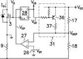
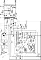
본 발명의 각 실시형태에서의 스위칭전원장치의 기본개념을 나타낸 블록회로도를 도 1에 나타낸다. 도 1에 나타내는 스위칭전원장치는, 직류전원(1)과, 직류전원(1)에 대하여 직렬로 접속된 트랜스(2)의 1차권선(2a) 및 스위칭소자로서의 MOS-FET(MOS형 전계효과트랜지스터)(3)와, 트랜스(2)의 2차권선(2b)에 접속된 출력정류 다이오드(4) 및 출력평활콘덴서(5)로 이루어지며 또한 직류출력전압 VOUT를 발생하는 출력정류평활회로(6)와, 직류출력전압 VOUT을 검출하는 전압검출수단(출력전압검출회로)(7)과, 전압검출수단(7)으로부터의 검출신호 VFB를 수신하고 또한 직류출력전압 VOUT의 레벨이 대략 일정해지도록 MOS-FET(3)의 온·오프기간을 제어하는 구동신호 VG를 발생하는 온·오프신호발생수단(25)을 가진 제어회로(8)와, 트랜스 (2)의 1차권선(2a) 또는 MOS-FET(3)에 흐르는 전류 ID를 전압으로서 검출하는 전류검출수단(전류검출용저항)(9)을 구비하고 있다. 제어회로(8)는, 전류검출수단(9)의 검출신호 VOCP의 전압이 기준전압 VDT의 레벨에 도달하지 않을 때에 낮은 전압(L) 레벨의 전류검출신호 VCP를 출력하여, 전류검출수단(9)의 검출신호 VOCP의 전압이 기준전압 VDT의 레벨을 넘었을 때에 높은 전압(H) 레벨의 전류검출신호 VCP를 출력하는 전류비교수단(전류검출용 컴퍼레이터)(27)과, MOS-FET(3)의 온으로부터 오프로의 전환시에 MOS-FET(3)의 게이트단자(제어단자)에 부여되는 구동신호 VG의 하강 에지를 검출하는 에지검출수단(28a)과, 에지검출수단(28a)이 구동신호 VG의 하강 에지를 검출했을 때에 전류비교수단(27)으로부터 전류검출신호 VCP를 취입하여 출력신호 VLD를 발생하는 부하판정수단(28b)을 가진다. 도 1에 나타내는 스위칭전원장치에서는, 부하판정수단(28b)의 출력신호 VLD가 낮은 전압(L) 레벨일 때에 경부하상태라고 판단하고, 부하판정수단(28b)의 출력신호 VLD가 높은 전압(H) 레벨일 때에 경부하보다 무거운 상태, 즉 중부하∼통상부하상태라고 판단한다. 또한, 도 2 이후에 나타내는 각 실시형태에서는 에지검출수단(28a) 및 부하판정수단(28b)이 D플립플롭(28)으로 구성된다.A block circuit diagram showing a basic concept of a switching power supply device in each embodiment of the present invention is shown in FIG. The switching power supply device shown in FIG. 1 has aprimary power line 2a and a MOS-FET (MOS field effect) as a switching element of a directcurrent power source 1 and atransformer 2 connected in series with the directcurrent power source 1. Transistor) 3, an output rectifying diode 4 and anoutput smoothing capacitor 5 connected to the secondary winding 2b of thetransformer 2, and an output rectifying smoothing circuit for generating a DC output voltage VOUT . (6), the voltage detecting means (output voltage detecting circuit) 7 for detecting the DC output voltage VOUT , and the detection signal VFB from the voltage detecting means 7 are received and the level of the DC output voltage VOUT is received. and a substantially constant to ensure MOS-FET (3) for turning on and with an on-off signal generating means 25 for generating the driving signal VG which controls the off-period control circuit 8, one of the transformer (2) Current detecting means (current detecting resistor) 9 is provided for detecting the current ID flowing through the vehicle winding 2a or the MOS-FET 3 as a voltage. Thecontrol circuit 8 outputs a current detection signal VCP having a low voltage (L) level when the voltage of the detection signal VOCP of the current detection means 9 does not reach the level of the reference voltage VDT , thereby detecting current. Current comparison means (current detection comparator) 27 for outputting a current detection signal VCP of a high voltage (H) level when the voltage of the detection signal VOCP of themeans 9 exceeds the level of the reference voltage VDT . and, the MOS-FET MOS-FET (3), the gate terminal edge detection means for detecting a falling edge of the drive signal VG given to the (control terminal) (28a) of the time switch (3) from on to off of the and has the edge detecting means (28a), the driving signal V load is determined whenG detects a falling edge of the accepts the current detection signal VCP from the current comparator means (27) for generating an output signal VLD means (28b). In the switching power supply apparatus shown in Figure 1, the output signal VLD has a high voltage of the load determining means (28b) the output signal VLD has a low voltage (L) level one when it is determined that the light load state, the load determining means (28b) of At the (H) level, it is determined that the state is heavier than the light load, that is, the medium to normal load. In addition, in each embodiment shown after FIG. 2, the edge detection means 28a and the load determination means 28b are comprised by the D flip-flop 28. As shown in FIG.

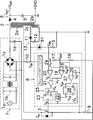
본 발명에 의한 스위칭전원장치를 타려식 플라이백형 DC-DC 컨버터에 적용한 실시형태를 도 2에 나타낸다. 도 2에 나타낸 실시형태의 타려식 플라이백형 DC-DC 컨버터는, 교류전원(1a)에 입력필터회로(1b)를 통해 접속된 정류 브리지회로(1c) 및 입력평활콘덴서(1d)로 구성된 직류전원(1)과, 직류전원(1)에 대하여 직렬로 접속된 트랜스(2)의 1차권선(2a) 및 MOS-FET(3)와, 트랜스(2)의 2차권선(2b)에 접속된 출력정류 다이오드(4) 및 출력평활콘덴서(5)로 이루어지고 또한 직류출력전압 VOUT을 발생하는 출력정류평활회로(6)와, 직류출력전압 VOUT를 검출하는 전압검출수단으로서의 출력전압검출회로(7)와, 출력전압검출회로(7)로부터의 검출신호 VFB을 수신하고 또한 출력정류평활회로(6)의 직류출력전압 VOUT이 대략 일정해지도록 MOS-FE T(3)의 온·오프기간을 제어하는 제어회로(8)와, 트랜스(2)의 1차권선(2a) 또는 MOS-FET(3)에 흐르는 전류 ID를 부전압으로서 검출하는 전류검출수단으로서의 전류검출용저항(9)과, 직류전원(1)을 구성하는 정류 브리지회로(1c)에 접속되고 또한 기동시에 제어회로(8)에 구동용전력을 공급하는 기동수단으로서의 기동저항(10)과, 트랜스(2)의 1차권선(2a) 및 2차권선(2b)에 전자적으로 결합하는 구동권선(2c)과, 구동권선(2c)에 접속된 정류 다이오드(11) 및 구동용평활콘덴서(12)로 이루어지고 또한 제어회로(8)를 구동하는 직류전압 VIN을 출력하는 보조정류평활회로(13)를 구비하고 있다. 출력전압검출회로(7)의 검출출력은, 포토커플러(14)를 구성하는 발광소자(14a)및 수광소자(14b)를 통해 트랜스(2)의 1차측에 전달되고, 수광소자(14b) 및 저항(15)의 접속점에 발생하는 전압 VFB이 출력전압검출회로(7)부터의 검출신호로서 제어회로(8)에 입력된다.2 shows an embodiment in which the switching power supply according to the present invention is applied to a flyback type DC-DC converter. The flyback type DC-DC converter of the embodiment shown in FIG. 2 is a direct current power source composed of a rectifyingbridge circuit 1c and aninput smoothing capacitor 1d connected to anAC power source 1a via an input filter circuit 1b. (1) and the primary winding 2a and MOS-FET 3 of thetransformer 2 connected in series with theDC power supply 1, and the secondary winding 2b of thetransformer 2, respectively. output rectifying diode (4) and is made of the output smoothing capacitor (5) in addition, the DC output voltage V and an output rectifying and smoothingcircuit 6 for generating anOUT, the DC output voltage the voltage detection means as the output voltage detection circuit for detecting a VOUT (7) and the MOS-FE T (3) are turned on so that the detection signal VFB from the output voltage detection circuit 7 is received and the DC output voltage VOUT of the outputrectification smoothing circuit 6 becomes substantially constant. The current detection number for detecting the current ID flowing through thecontrol circuit 8 for controlling the off period and the primary winding 2a of thetransformer 2 or the MOS-FET 3 as a negative voltage. A startingresistor 10 serving as a starting means connected to a current detectingresistor 9 as a function and a rectifyingbridge circuit 1c constituting theDC power supply 1 and supplying driving power to thecontrol circuit 8 at the start-up; And a drive winding 2c electronically coupled to theprimary windings 2a and thesecondary windings 2b of thetransformer 2, arectifier diode 11 and a driving smoothing capacitor connected to the driving winding 2c. An auxiliaryrectification smoothing circuit 13, which is composed of 12 and outputs a DC voltage VIN for driving thecontrol circuit 8, is provided. The detection output of the output voltage detection circuit 7 is transmitted to the primary side of thetransformer 2 via thelight emitting element 14a and thelight receiving element 14b constituting thephotocoupler 14, and thelight receiving element 14b and The voltage VFB generated at the connection point of theresistor 15 is input to thecontrol circuit 8 as a detection signal from the output voltage detection circuit 7.

제어회로(8)는, 트랜스(2)의 1차권선(2a) 또는 MOS-FET(3)에 흐르는 최대전류치를 규정하는 기준전압 VRC를 발생하는 기준전압발생수단으로서의 기준전원(16)과, 전류검출용저항(9)에 의해 검출된 부전압의 레벨을 변환하는 레벨 시프트용 저항(17, 18)과, 레벨 시프트된 전류검출용저항(9)의 검출신호 VOCP의 전압 레벨이 기준전원(16)의 기준전압 VRC의 레벨에 도달했을 때에 MOS-FET(3)를 오프상태로 하는 높은 전압(H) 레벨의 신호 V1를 출력하는 과전류제한용 컴퍼레이터(19)와, 레벨 시프트된 전류검출용저항(9)의 검출신호 VOCP의 전압 레벨이 출력전압검출회로(7)부터의 검출신호 VFB의 전압 레벨에 도달했을 때에 높은 전압(H) 레벨의 신호 V2를 출력하는 전류모드제어용 컴퍼레이터(20)와, 과전류제한용 컴퍼레이터(19)의 출력신호 V1와 전류모드제어용 컴퍼레이터(20)의 출력신호 V2와의 논리합신호 V3를 출력하는 OR게이트(21)와, MOS-FET(3)가 오프하고 나서 일정한 시간이 경과할 때마다 펄스신호 V4를 출력하는 펄스발생기(22)와, 펄스발생기(22)의 펄스신호 V4에 의해 세트상태가 되어 MOS-FET(3)의 게이트단자에 높은 전압(H) 레벨의 구동신호 VG를 출력하고, OR 게이트(21)의 논리합신호 V3에 의해 리세트상태가 되어 MOS-FET(3)의 게이트단자에 낮은 전압(L) 레벨의 구동신호 VG를 출력하는 R-S 플립플롭(23)과, 기동저항(10) 또는 보조정류평활회로(13)로부터의 직류전압 VIN이 구동전압에 도달했을 때에 제어회로(8)를 구성하는 각 소자(16∼28)에 구동용 직류전력을 공급하고 또한 직류 전압 VIN이 정지전압까지 저하했을 때에 상기의 각 소자(16∼28)에의 구동용 직류전력의 공급을 정지하는 제어전원회로(24)와, 도시하지 않은 부하의 상태를 판정하기 위한 전압 레벨을 규정하는 기준전압 VDT을 발생하는 기준전원(26)과, 레벨 시프트된 전류검출용저항(9)의 검출신호 VOCP의 전압 레벨이 기준전원(26)의 기준전압 VDT의 레벨에 도달하지 않았을 때에 낮은 전압(L) 레벨의 전류검출신호 VCP를 출력하고, 검출신호 VOCP의 전압 레벨이 기준전원(26)의 기준전압 VDT의 레벨을 넘었을 때에 높은 전압(H) 레벨의 전류검출신호 VCP를 출력하는 전류비교수단으로서의 전류검출용 컴퍼레이터(27)와, MOS-FET(3)의 온으로부터 오프에의 전환시에 게이트단자에 부여되는 구동신호 VG의 하강 에지가 클록입력단자(CLK)에 입력되었을 때, 전류검출용 컴퍼레이터(27)로부터 출력된 전류검출신호 VCP를 신호입력단자(D)를 통해 취하여 넣고, 전류검출신호 VCP의 전압 레벨과 대략 동일한 전압 레벨의 출력신호 VLD를 신호출력단자(Q)로부터 발생함과 동시에, 구동신호 VG의 하강 에지가 클록입력단자(CLK)에 입력되고 나서 다시 입력되기까지의 동안에, 출력신호 VLD의 전압 레벨을 유지하는 D플립플롭(28)을 가진다. 도 2에 나타내는 전류모드제어용 컴퍼레이터(20), OR 게이트(21), 펄스발생기(22) 및 R-S 플립플롭(23)은, 도 1에 나타내는 온·오프신호발생수단(25)을 구성한다. 펄스발생기(22)는, D플립플롭(28)의 출력신 호 VLD가 낮은 전압(L) 레벨일 때에 펄스신호 V4의 발생주기를 길게 함으로써, R-S 플립플롭(23)으로부터 MOS-FET(3)의 게이트단자에 부여되는 구동신호 VG의 오프시간을 연장하여 구동신호 VG의 발진주파수를 저하시키고, D플립플롭(28)의 출력신호 VLD가 높은 전압(H) 레벨일 때에 펄스신호 V4의 발생주기를 짧게 함으로써, R-S 플립플롭(23)으로부터 MOS-FET(3)의 게이트단자에 부여되는 구동신호 VG의 오프시간을 단축하고 구동신호 VG의 발진주파수를 증가시키는 발진제어수단을 가진다. 구동신호 VG의 오프시간, 즉 낮은 전압(L) 레벨이 되는 기간은, 예를 들면 10[μs]∼50[μs]정도의 범위로 설정된다. 또한, 레벨 시프트된 전류검출용저항(9)의 검출신호 VOCP의 전압레벨, 즉 레벨 시프트용 저항(17, 18)의 접속점 전압 VOCP의 레벨은, 예를 들면 기동전의 상태로 0[V], 기동후에 M0S-FET(3)에 흐르는 전류 ID가 제로일 때에 1.5[V]가 되도록 각 저항(17, 18)의 저항치를 적절히 선택함으로써 설정된다.Thecontrol circuit 8 includes areference power supply 16 as reference voltage generating means for generating a reference voltage VRC that defines a maximum current value flowing through the primary winding 2a or the MOS-FET 3 of thetransformer 2; The voltage level of the detection signal VOCP of thelevel shifting resistors 17 and 18 for converting the level of the negative voltage detected by the current detectingresistor 9 and the level shifted current detectingresistor 9 is referenced. and a MOS-FET (3) a comparator (19) for over-current to output a signal V1 of the high voltage (H) level to the off state limit when it has reached the base level of the voltage VRC of thepower source 16, a level shift When the voltage level of the detection signal VOCP of the detectedcurrent detection resistor 9 reaches the voltage level of the detection signal VFB from the output voltage detection circuit 7, the signal V2 of the high voltage (H) level is output. currentmode control comparator 20 and the output signal V1 and the current mode control of the comparator (19) for over-current limit comparator lesOR gate 21 and, MOS-FET pulse generator (3) is off and then outputs a pulse signal V4 each time the predetermined time and outputting the output signal V2 with the logical sum signal V3 of the emitter (20) 22, apulse generator 22, pulse signal V4 is the state set by the output a drive signal VG of the MOS-FET (3) high voltage (H) level to the gate terminal of, and of the OR gate (21 RS flip-flop 23 and start-upresistor 10 which are reset by the logic sum signal V3 and output the driving signal VG having a low voltage (L) level to the gate terminal of the MOS-FET 3. Alternatively, when the DC voltage VIN from the auxiliaryrectifier smoothing circuit 13 reaches the driving voltage, the driving DC power is supplied to each of theelements 16 to 28 constituting thecontrol circuit 8 and the DC voltage VIN is increased. The controlpower supply circuit 24 which stops the supply of the driving DC power to each of the above-describedelements 16 to 28 when the voltage is lowered to the stop voltage is not shown. The voltage level of thereference power supply 26 for generating the reference voltage VDT for defining the voltage level for determining the state of the unloaded load and the detection signal VOCP of the level shiftedcurrent detection resistor 9 is thereference power supply 26. When the level of the reference voltage VDT is not reached, the current detection signal VCP of the low voltage (L) level is outputted, and the voltage level of the detection signal VOCP changes the level of the reference voltage VDT of thereference power supply 26. Thecurrent detection comparator 27 serving as a current comparison means for outputting the current detection signal VCP having a high voltage (H) level when exceeded, and the gate terminal when switching from on to off of the MOS-FET 3. When the falling edge of the drive signal VG applied is inputted to the clock input terminal CLK, the current detection signal VCP output from the current detectingcomparator 27 is taken in through the signal input terminal D, and the current is input. Voltage level approximately equal to voltage level of detection signal VCP An output signal VLD of the bell and at the same time generated from the signal output terminal (Q), while to the falling edge of the drive signal VG is the clock input then is input to the terminal (CLK) is input again, the voltage of the output signal VLD It has aD flip flop 28 that maintains the level. The currentmode control comparator 20, theOR gate 21, thepulse generator 22, and the RS flip-flop 23 shown in FIG. 2 constitute the on / off signal generating means 25 shown in FIG. Thepulse generator 22 extends the generation period of the pulse signal V4 when the output signal VLD of the D flip-flop 28 is at a low voltage (L) level, thereby MOS-FET ( 3) to extend the off time of the driving signal VG is applied to the gate terminal and lowering the oscillation frequency of the drive signal VG of a pulse when the output signal VLD has a high voltage (H) level of the D flip-flop 28 By shortening the generation period of the signal V4 , an oscillation that shortens the off time of the drive signal VG applied to the gate terminal of the MOS-FET 3 from the RS flip-flop 23 and increases the oscillation frequency of the drive signal VG. Has control means. The off time of the drive signal VG , that is, the period at which the low voltage L level is set, is set in the range of about 10 [μs] to 50 [μs], for example. In addition, the voltage level of the detection signal VOCP of the level shiftedcurrent detection resistor 9, that is, the level of the connection point voltage VOCP of thelevel shifting resistors 17 and 18 is, for example, 0 [V] in the state before starting. ] Is set by appropriately selecting the resistance values of theresistors 17 and 18 so as to be 1.5 [V] when the current ID flowing through the M0S-FET 3 is zero after startup.

도 3(A)∼(E)는, 중부하∼통상 부하상태로부터 경부하상태로 이행할 때의 MOS-FET(3)의 게이트단자에 부여되는 구동신호 VG, MOS-FET(3)의 드레인전류 ID, 레벨 시프트용저항(17, 18)의 접속점의 전압 VOCP, 전류검출용 컴퍼레이터(27)의 전류검출신호 VCP 및 D플립플롭(28)의 출력신호 VLD의 각 파형을 각각 나타낸 것이다. 즉, 중부하∼통상부하상태에 있어서, 도3(A)에 도시한 바와 같이 시각 t0에서 MOS- FET(3)의 게이트단자에 부여되는 구동신호 VG의 전압 레벨이 낮은 전압(L) 레벨로부터 높은 전압(H) 레벨이 되고, MOS-FET(3)가 턴온하면, 용량성의 단락전류가 MOS-FET(3)에 순간적으로 흘러, 도 3(B)에 도시한 바와 같이 드레인전류 ID가 급격히 증가한다. 이에 따라, 도 3(C)에 도시한 바와 같이 레벨 시프트용 저항(17, 18)의 접속점의 전압 VOCP이 기준전원(26)의 기준전압 VDT의 레벨이하까지 저하하기 때문에, 도 3(D)에 도시한 바와 같이 전류검출용 컴퍼레이터(27)에서 높은 전압(H) 레벨의 전류검출신호 VCP가 출력된다. 그 후, 시각 t1에서 레벨 시프트용 저항(17,18)의 접속점의 전압 VOCP이 기준전원(26)의 기준전압 VDT의 레벨보다 높아지면, 전류검출신호 VCP의 전압 레벨이 높은 전압(H) 레벨로부터 낮은 전압(L) 레벨이 된다.3A to 3E show driving signalsVG and MOS-FETs 3 applied to the gate terminals of the MOS-FETs 3 when transitioning from a heavy load to a normal load state. Waveforms of the drain current ID , the voltage VOCP at the connection point of thelevel shift resistors 17 and 18, the current detection signal VCP of thecurrent detection comparator 27, and the output signal VLD of the D flip-flop 28. Will be shown respectively. That is, the heavy-load condition in normal ~, Fig. 3 (A) is a low voltage level of the driving signal VG given at time t0 to the gate terminal of the MOS- FET (3) voltage, as (L) level as it is shown in the When the MOS-FET 3 is turned on at a high voltage H level, the capacitive short-circuit current flows momentarily through the MOS-FET 3, and the drain current ID as shown in Fig. 3B. Increases rapidly. As a result, as shown in FIG. 3C, the voltage VOCP at the connection point of thelevel shifting resistors 17 and 18 falls to the level below the reference voltage VDT of thereference power supply 26, and therefore, FIG. As shown in D), thecurrent detection comparator 27 outputs a current detection signal VCP having a high voltage (H) level. Subsequently, when the voltage VOCP of the connection point of thelevel shifting resistors 17 and 18 becomes higher than the level of the reference voltage VDT of thereference power supply 26 at time t1, the voltage level of the current detection signal VCP is high ( From the H) level to the low voltage L level.

MOS-FET(3)가 온상태가 되면, 도 3(B)에 도시한 바와 같이 드레인전류 ID가 직선적으로 증가함과 동시에, 도 3(C)에 도시한 바와 같이 레벨 시프트용 저항(17, 18)의 접속점의 전압 VOCP이 직선적으로 저하한다. 레벨 시프트용 저항(l7, 18)의 접속점의 전압 VOCP이 시각 t2에서 기준전원(26)의 기준전압 VDT의 레벨이하가 되면, 도 3(D)에 도시한 바와 같이 전류검출용 컴퍼레이터(27)의 전류검출신호 VCP의 전압 레벨이 낮은 전압(L) 레벨로부터 높은 전압(H) 레벨로 전환된다. 도 3(A)에 도시한 바와 같이, MOS-FET(3)의 게이트단자에 부여되는 구동신호 VG의 전압 레벨이 시 각 t3에서 높은 전압(H) 레벨로부터 낮은 전압(L) 레벨이 되면, MOS-FET(3)가 온상태로부터 오프상태로 전환된다. 이 때, 전류검출용 컴퍼레이터(27)의 전류검출신호 VCP의 전압 레벨은 도 3(D)에 도시한 바와 같이 높은 전압(H) 레벨이기 때문에, 시각 t0 이전의 부하의 상태가 경부하상태였던 경우는 도3(E)의 실선부로 도시한 바와 같이 D플립플롭(28)의 신호출력단자(Q)로부터 출력되는 신호 VLD의 전압 레벨이 낮은 전압(L) 레벨로부터 높은 전압(H) 레벨로 전환되고, 시간 t0 이전의 부하의 상태가 중부하∼통상 부하상태였던 경우는 도 3(E)의 파선부에 도시한 바와 같이 D플립플롭(28)의 신호출력단자(Q)로부터 출력되는 신호 VLD의 전압 레벨이 높은 전압(H) 레벨로 유지된다. 따라서, D플립플롭(28)의 신호출력단자(Q)로부터 높은 전압(H) 레벨의 출력신호 VLD가 출력되었을 때는 중부하∼통상 부하상태라고 판단하여, 펄스발생기(22)로부터 짧은 주기의 펄스신호 V4가 발생한다.When the MOS-FET 3 is turned on, the drain current ID increases linearly as shown in Fig. 3B, and thelevel shifting resistor 17 is shown in Fig. 3C. The voltage VOCP at the connection point of 18) decreases linearly. When the voltage VOCP at the connection point of thelevel shifting resistors 17 and 18 falls below the level of the reference voltage VDT of thereference power supply 26 at time t2, the current detection comparator is shown in Fig. 3D. The voltage level of the current detection signal VCP of (27) is switched from the low voltage (L) level to the high voltage (H) level. As shown in Fig. 3 (A), MOS-FET (3) when the two when the voltage level of the drive signal VG is applied to the gate terminal of the low voltage (L) level from a high voltage (H) level at the respective t3 The MOS-FET 3 is switched from the on state to the off state. At this time, since the voltage level of the current detection signal VCP of thecurrent detection comparator 27 is a high voltage (H) level as shown in Fig. 3D, the state of the load before time t0 is light. In the case of the lower state, as shown by the solid line in Fig.3E, the voltage level of the signal VLD output from the signal output terminal Q of the D flip-flop 28 is lower than the low voltage L level. H) If the state of the load before the time t0 is in the medium to normal load state is changed to the H) level, the signal output terminal Q of the D flip-flop 28 as shown by the broken line in Fig. 3E. The voltage level of the signal VLD outputted fromC1 ) is maintained at a high voltage H level. Therefore, when the output signal VLD having a high voltage H level is output from the signal output terminal Q of the D flip-flop 28, it is determined to be a heavy load to a normal load state, and thepulse generator 22 has a short period of time. The pulse signal V4 is generated.

MOS-FET(3)가 오프상태가 되면, MOS-FET(3)자신의 응답지연 또는 MOS-FET(3)의 부유용량에 의한 미러효과 등에 의해 도 3(B)에 도시한 바와 같이 드레인전류 ID가 완만하게 감소함과 동시에, 도 3(C)에 도시한 바와 같이 레벨 시프트용 저항(17, 18)의 접속점의 전압 VOCP이 완만하게 상승한다. 레벨 시프트용 저항(17, 18)의 접속점의 전압 VOCP가 시각 t4에서 기준전원(26)의 기준전압 VDT의 레벨보다 높아지면, 도 3(D)에 도시한 바와 같이 전류검출용 컴퍼레이터(27)의 전류검출신호 VCP 의 전압 레벨이 높은 전압(H) 레벨로부터 낮은 전압(L) 레벨로 전환되고, 시각 t5에 도 3(B)에 도시한 바와 같이 드레인전류 ID가 약 제로가 된다.When the MOS-FET 3 is turned off, the drain current as shown in Fig. 3B due to the delay of the response of the MOS-FET 3 itself or the mirror effect caused by the stray capacitance of the MOS-FET 3 or the like. While the ID decreases gently, as shown in Fig. 3C, the voltage VOCP at the connection point of thelevel shifting resistors 17, 18 rises slowly. If the voltage VOCP at the connection point of thelevel shifting resistors 17 and 18 becomes higher than the level of the reference voltage VDT of thereference power supply 26 at time t4, the current detection comparator is shown in Fig. 3D. The voltage level of the current detection signal VCP at (27) is changed from the high voltage (H) level to the low voltage (L) level, and the drain current ID is approximately zero at time t5 as shown in Fig. 3B. Becomes

중부하∼통상부하상태로부터 경부하상태로 이행할 때, 도 3(A)에 도시한 바와 같이 시각 t6에서 MOS-FET(3)의 게이트단자에 부여되는 구동신호 VG의 전압 레벨이 낮은 전압(L) 레벨로부터 높은 전압(H) 레벨이 되어, MOS-FET(3)가 턴온하면, 상술의 시각 t0∼t1일 때와 같이 용량성의 단락전류가 MOS-FET(3)에 순간적으로 흘러, 도 3(B)에 도시한 바와 같이 드레인전류 ID가 급격히 증가한다. 이에 따라, 도 3(C)에 도시한 바와 같이 레벨 시프트용 저항(17,18)의 접속점의 전압 VOCP이 기준전원(26)의 기준전압 VDT의 레벨이하까지 저하하기 때문에, 도 3(D)에 도시한 바와 같이 전류검출용 컴퍼레이터(27)에서 높은 전압(H) 레벨의 전류검출신호 VCP가 출력된다. 그 후, 시각 t7에서 레벨 시프트용 저항(17, 18)의 접속점의 전압 VOCP이 기준전원(26)의 기준전압 VDT의 레벨보다 높아지면, 전류검출신호 VCP의 전압 레벨이 높은 전압(H) 레벨로부터 낮은 전압(L) 레벨이 된다. MOS-FET(3)가 온상태가 되면, 도 3(B)에 도시한 바와 같이 드레인전류 ID가 직선적으로 증가함과 동시에, 도 3(C)에 도시한 바와 같이 레벨 시프트용 저항(17, 18)의 접속점의 전압 VOCP이 직선적으로 저하한다. 경부하일 때는, MOS-FET(3)의 온시간이 중부하∼통상부하일 때의 온 시간 t0∼t3보다도 짧아지기 때문에, 도 3(A)에 도시한 바와 같이 비교적 빠른 시각 t8에서 구동신호 VG의 전압 레벨이 높은 전압(H) 레벨로부터 낮은 전압(L) 레벨이 되어, MOS-FET(3)가 온상태로부터 오프상태로 전환된다. 이 때문에, 도 3(C)에 도시한 바와 같이 레벨 시프트용저항(17, 18)의 접속점의 전압 VOCP이 기준전원(26)의 기준전압 VDT의 레벨에 도달하지 않고, 전류검출용 컴퍼레이터(27)의 전류검출신호 VCP는 도 3(D)에 도시한 바와 같이 낮은 전압(L) 레벨을 유지한다. 이에 따라, D플립플롭(28)의 신호출력단자(Q)로부터 출력되는 신호 VLD의 전압 레벨이 도 3(E)에 도시한 바와 같이 시각 t8에서 높은 전압(H) 레벨로부터 낮은 전압(L) 레벨로 전환된다. 따라서, D플립플롭(28)의 신호출력단자(Q)로부터 낮은 전압(L) 레벨의 출력신호 VLD가 출력되었을 때는 경부하상태라고 판단하고, 펄스발생기(22)로부터 긴 주기의 펄스신호 V4가 발생한다.When transitioning from the heavy load to the normal load state, the voltage level of the drive signal VG applied to the gate terminal of the MOS-FET 3 is low at time t6 as shown in FIG. When the MOS-FET 3 is turned on from the voltage L level to the high voltage H level, capacitive short-circuit current is instantaneously provided to the MOS-FET 3 as in the time t0 to t1 described above. As shown in FIG. 3 (B), the drain current ID increases rapidly. As a result, as shown in FIG. 3C, the voltage VOCP at the connection point of thelevel shifting resistors 17 and 18 decreases below the level of the reference voltage VDT of thereference power supply 26. As shown in D), thecurrent detection comparator 27 outputs a current detection signal VCP having a high voltage (H) level. Thereafter, when the voltage VOCP of the connection point of thelevel shifting resistors 17 and 18 becomes higher than the level of the reference voltage VDT of thereference power supply 26 at time t7 , the voltage level of the current detection signal VCP is high. The voltage (L) level becomes low from the (H) level. When the MOS-FET 3 is turned on, the drain current ID increases linearly as shown in Fig. 3B, and thelevel shifting resistor 17 is shown in Fig. 3C. , 18) and the voltage VOCP at the connection point drops linearly. At light loads, the on-time of the MOS-FET3 is shorter than the on-times t0 to t3 at heavy to normal loads, so that the drive signal is relatively fast at time t8 as shown in Fig. 3A. The voltage level of VG becomes from the high voltage H level to the low voltage L level, so that the MOS-FET 3 is switched from the on state to the off state. Therefore, as shown in Fig. 3C, the voltage VOCP at the connection point of thelevel shifting resistors 17 and 18 does not reach the level of the reference voltage VDT of thereference power supply 26, and the current detecting comp The current detection signal VCP of theradar 27 maintains a low voltage (L) level as shown in Fig. 3D. Accordingly, the voltage level of the signal VLD output from the signal output terminal Q of the D flip-flop 28 is low from the high voltage H level at time t8 as shown in Fig. 3E. ) Level is converted. Therefore, when the output signal VLD having a low voltage (L) level is output from the signal output terminal Q of the D flip-flop 28, it is determined to be a light load state, and the pulse signal V of a long period from thepulse generator 22 is determined.4 occurs.

다음에, 도 2에 나타내는 타려식 플라이백형 DC-DC 컨버터의 동작을 설명한다. 기동시에, 직류전원(1)으로부터 기동저항(10)을 통해 보조정류평활회로(13)의 구동용평활콘덴서(12)에 충전전류가 흐르고, 구동용평활콘덴서(12)의 충전전압 VIN이 구동전압에 도달하면, 제어회로(8)내의 제어전원회로(24)가 구동되어, 제어회로(8)를 구성하는 각 소자(16∼28)에 구동용 직류전력이 공급된다. 이에 따라, 펄스발생기(22)가 구동되어, 펄스발생기(22)로부터의 펄스신호 V4가 R-S 플립플롭(23)의 세트단자(S)에 입력되면, R-S 플립플롭(23)이 세트상태가 되기 때문에, R-S 플립플롭(23)으로부터 MOS-FET(3)의 게이트단자에 높은 전압(H) 레벨의 구동신호 VG가 부여되어, MOS-FET(3)가 온상태가 된다. 이 때, MOS-FET(3)에 흐르는 드레인전류 ID가 직선적으로 증가함과 동시에, 전류검출용저항(9)의 검출신호의 레벨 시프트용 저항(17, 18)의 접속점에서의 전압 VOCP이 직선적으로 저하한다. 레벨 시프트용 저항(17, 18)의 접속점의 전압 VOCP이 기준전원(16)의 기준전압 VRC의 레벨에 도달하면, 과전류제한용 컴퍼레이터(19)로부터 높은 전압(H) 레벨의 신호 V1가 출력된다. 한편, 기동시의 출력전압검출회로(7)로부터의 검출신호 VFB의 전압 레벨은 거의 제로이기 때문에, 전류모드제어용 컴퍼레이터(20)로부터 낮은 전압(L) 레벨의 신호 V2가 출력된다. 이에 따라, OR 게이트(21)로부터 높은 전압(H) 레벨의 논리합신호 V3가 출력되어, R-S 플립플롭(23)의 리세트단자(R)에 입력되어 리세트상태가 되기 때문에, R-S 플립플롭(23)으로부터 MOS-FET(3)의 게이트단자에 낮은 전압(L) 레벨의 구동신호 VG가 부여되어 MOS-FET(3)이 오프상태가 되어, MOS-FET(3)에 흐르는 드레인전류ID가 대략 제로가 된다. MOS-FET(3)가 오프하고 나서 일정시간이 경과하면, 펄스발생기(22)의 펄스신호 V4가 다시 R-S 플립플롭(23)의 세트단자(S)에 입력되어 세트상태가 되고, R-S 플립플롭(23)으로부터 MOS-FET(3)의 게이트단자에 높은 전압 (H) 레벨의 구동신호 VG가 부여되어 MOS-FET(3)가 다시 온상태가 된다. 이상의 MOS-FET(3)의 온·오프동작의 반복에 의해, 2차측의 출력정류평활회로(6)의 직류출력전압 VOUT가 직선적으로 상승하고, 이에 따라 구동용평활콘덴서(12)의 충전전압 VIN은 직선적으로 저하하지만, 트랜스(2)의 2차권선(2b)의 전압에 비례하는 전압이 구동권선(2c)에 발생하기 때문에, 직류출력전압(VOUT)의 상승에 따라 보조정류평활회로(13)로부터의 직류전압 VIN이 직선적으로 상승한다. 이 때문에, 제어회로(8)내의 제어전원회로(24)에 인가되는 직류전압 VIN은 정지전압부근까지 저하한 후, 다시 직선적으로 상승한다. 따라서, 기동시 이후에는 보조정류평활회로(13)로부터의 직류전압 VIN에 의해 제어회로(8)내의 제어전원회로(24)가 구동된다. 2차측의 출력정류평활회로(6)의 직류출력전압 VOUT의 상승에 따라, 출력전압검출회로(7)의 검출신호 VFB의 전압도 O[V]로부터 직선적으로 상승한다.Next, the operation of the hitting flyback type DC-DC converter shown in FIG. 2 will be described. At the start-up, a charging current flows from theDC power supply 1 through the startingresistor 10 to thedriving smoothing capacitor 12 of the auxiliaryrectification smoothing circuit 13, so that the charging voltage VIN of thedriving smoothing capacitor 12 isreduced . When the drive voltage is reached, the controlpower supply circuit 24 in thecontrol circuit 8 is driven, and driving DC power is supplied to each of theelements 16 to 28 constituting thecontrol circuit 8. Accordingly, when thepulse generator 22 is driven and the pulse signal V4 from thepulse generator 22 is input to the set terminal S of the RS flip-flop 23, the RS flip-flop 23 is set to the set state. since, the drive signal VG of the high voltage (H) level to the gate terminal of the MOS-FET (3) provided from the RS flip-flop 23, it is in a state the MOS-FET (3) oN. At this time, the drain current ID flowing through the MOS-FET 3 increases linearly, and the voltage VOCP at the connection point of thelevel shifting resistors 17 and 18 of the detection signal of the current detectingresistor 9 is increased. This falls linearly. When the voltage VOCP at the connection point of thelevel shifting resistors 17 and 18 reaches the level of the reference voltage VRC of thereference power supply 16, the signal V1 of the high voltage (H) level from theovercurrent limiting comparator 19 is reached. Is output. On the other hand, since the voltage level of the detection signal VFB from the output voltage detection circuit 7 at startup is almost zero, the signal V2 of low voltage (L) level is output from the currentmode control comparator 20. As a result, a logic sum signal V3 having a high voltage (H) level is output from theOR gate 21 and input to the reset terminal R of the RS flip-flop 23 to be in a reset state. A low voltage (L) level drive signalVG is applied to the gate terminal of the MOS-FET 3 from the 23, and the MOS-FET 3 is turned off, and the drain current flowing through the MOS-FET 3 flows. ID is approximately zero. When a predetermined time has elapsed since the MOS-FET 3 is turned off, the pulse signal V4 of thepulse generator 22 is again input to the set terminal S of the RS flip-flop 23 to be in the set state, and the RS flip a drive signal of a high voltage VG (H) level to the gate terminal of the MOS-FET (3) from theflop 23 is provided with the MOS-FET (3) is again turned on. By repeating the above ON / OFF operation of the MOS-FET 3, the DC output voltage VOUT of the outputrectification smoothing circuit 6 on the secondary side rises linearly, thereby charging thedriving smoothing capacitor 12. Although the voltage VIN decreases linearly, a voltage proportional to the voltage of the secondary winding 2b of thetransformer 2 is generated in the driving winding 2c, so that the auxiliary rectification is increased in accordance with the rise of the DC output voltage VOUT . The DC voltage VIN from the smoothingcircuit 13 rises linearly. Therefore, the control direct voltage VIN is applied to the controlpower supply circuit 24 in thecircuit 8 is then lowered to near the termination voltage, again a linear rise. Therefore, after startup, the controlpower supply circuit 24 in thecontrol circuit 8 is driven by the DC voltage VIN from the auxiliaryrectification smoothing circuit 13. As the DC output voltage VOUT of the outputrectification smoothing circuit 6 on the secondary side rises, the voltage of the detection signal VFB of the output voltage detection circuit 7 also rises linearly from O [V].

출력전압검출회로(7)부터의 검출신호 VFB의 전압 레벨이 기준전원(16)의 기준전압 VRC의 레벨보다도 높아져, 레벨 시프트용저항(17, 18)의 접속점의 전압 VOCP이 출력전압검출회로(7)로부터의 검출신호 VFB의 전압 레벨에 도달하면, 전류모드제어용 컴퍼레이터(20)로부터 높은 전압(H) 레벨의 신호 V2가 출력된다. 한편, 과전류제한용 컴퍼레이터(19)로부터는 낮은 전압(L) 레벨의 신호 V1가 출력되기 때문에, OR 게이트(21)로부터 높은 전압(H) 레벨의 논리합신호 V3가 출력되고, R-S 플립플롭(23)의 리세트단자(R)에 입력되어 리세트상태가 된다. 이에 따라, R-S 플립플롭(23)으로부터 MOS-FET(3)의 게이트단자에 낮은 전압(L) 레벨의 구동신호 VG가 부여되어 MOS-FET(3)가 오프상태가 되기 때문에, MOS-FET(3)에 흐르는 드레인전류 ID가 약 제로가 된다. 이 때, 트랜스(2)의 2차권선(2b)로부터 출력정류평활회로(6)를 통해 도시하지 않은 부하에 출력전류 IOUT가 흐르고, 직선적으로 증가해 나간다. 그리고, 2차측의 출력정류평활회로(6)의 직류출력전압 VOUT이 출력전압검출회로(7)를 구성하는 각 소자의 여러가지정수로 결정되는 검출전압(예를 들면, 출력단자간의 분압저항의 분압비를 R2/(R1+R2), 제너 다이오드의 제너 전압을 VZ[V], NPN 트랜지스터의 베이스·이미터간의 전압을 VBE(0.6∼0.7정도)[V]로 하면, {(R1+R2)/R2}×(VZ+VBE)[V]}에 도달하였을 때, 기동상태로부터 통상 동작상태로 이행하여, 보조정류평활회로(13)로부터의 직류전압 VIN이 대략 일정하게 됨과 동시에, 2차측의 출력정류평활회로(6)의 직류출력전압 VOUT 및 부하에 흐르는 출력전류 IOUT가 대략 일정해진다.The voltage level of the detection signal VFB from the output voltage detection circuit 7 becomes higher than the level of the reference voltage VRC of thereference power supply 16, so that the voltage VOCP at the connection point of thelevel shifting resistors 17 and 18 detects the output voltage. When the voltage level of the detection signal VFB from the circuit 7 is reached, the high voltage (H) level signal V2 is output from the currentmode control comparator 20. On the other hand, since the low voltage (L) level signal V1 is output from theovercurrent limiting comparator 19, the logic sum signal V3 of the high voltage (H) level is output from theOR gate 21, and RS flip. It is input to the reset terminal R of theflop 23, and it becomes a reset state. Thereby, the MOS-FET (3), the driving signal VG of the low voltage (L) level to the gate terminal of the grant from the RS flip-flop 23 because the OFF state MOS-FET (3), MOS-FET The drain current ID flowing in (3) becomes about zero. At this time, the output current IOUT flows from the secondary winding 2b of thetransformer 2 to the load which is not shown in figure through the outputrectification smoothing circuit 6, and increases linearly. Then, the DC output voltage VOUT of the outputrectification smoothing circuit 6 on the secondary side is determined by various constants of the respective elements constituting the output voltage detecting circuit 7 (for example, the voltage divider resistance between the output terminals). If the voltage division ratio is R2 / (R1 + R2 ), the zener voltage of the zener diode is VZ [V], and the voltage between the base and emitter of the NPN transistor is VBE (about 0.6 to 0.7) [V]. When {(R1 + R2 ) / R2 } × (VZ + VBE ) [V]} is reached, the state shifts from the start state to the normal operation state, and the DC voltage from the auxiliaryrectification smoothing circuit 13 is reached. While VIN becomes substantially constant, the DC output voltage VOUT of the outputrectification smoothing circuit 6 on the secondary side and the output current IOUT flowing through the load become substantially constant.

통상의 부하상태에 있어서, R-S 플립플롭(23)으로부터 MOS-FET(3)의 게이트단자에 도 4(B)에 나타내는 높은 전압(H) 레벨의 구동신호 VG가 부여되어, MOS-FET (3)가 온상태가 되면, 도 4(A)에 도시한 바와 같이 MOS-FET(3)에 흐르는 드레인전 류 ID가 직선적으로 증가함과 동시에, 레벨 시프트용 저항(17, 18)의 접속점의 전압 VOCP가 도 4(D)에 도시한 바와 같이 직선적으로 저하한다. 여기서, 도 4(D)에 도시한 바와 같이 통상부하시의 출력전압검출회로(7)로부터의 검출신호 VFB의 전압 레벨은 기준전원(26)의 기준전압 VDT의 레벨보다 낮기 때문에, 레벨 시프트용저항(17, 18)의 접속점의 전압 VOCP는 기준전원(26)의 기준전압 VDT의 레벨을 넘어 출력전압검출회로(7)로부터의 검출신호 VFB의 전압 레벨까지 저하한다. 이 때문에, 전류검출용 컴퍼레이터(27)에서 높은 전압(H) 레벨의 전류검출신호 VCP가 출력된다. 그리고, 도 4(D)에 도시한 바와 같이 레벨 시프트용 저항(17, 18)의 접속점의 전압 VOCP가 출력전압검출회로(7)로부터의 검출신호 VFB의 전압 레벨에 도달하면, 전류모드제어용 컴퍼레이터(20)로부터 높은 전압(H) 레벨의 신호 V2가 출력된다. 한편, 과전류제한용 컴퍼레이터(19)로부터는 낮은 전압(L) 레벨의 신호 V1가 출력되기 때문에, OR 게이트(21)로부터 높은 전압(H) 레벨의 논리화신호 V3가 출력되어, R-S 플립플롭(23)의 리세트단자(R)에 입력되어 리세트상태가 된다. 이에 따라, 도 4(B)에 도시한 바와 같이 R-S 플립플롭(23)으로부터 MOS-FET(3)의 게이트단자에 부여되는 구동신호 VG의 전압 레벨이 높은 전압(H) 레벨로부터 낮은 전압(L) 레벨이 되어, MOS-FET(3)가 온상태로부터 오프상태로 전환되기 때문에, 도 4(A)에 도시한 바와 같이 MOS-FET(3)에 흐르는 드레인전류 ID가 거의 제로가 된다. 이 때, D플립플롭(28)의 클록입력단자(CLK)에 도 4(B)에 나타내는 구동신호 VG의 하강 에지(화살표)가 입력됨과 동시에, 신호입력단자(D)에 전류검출용 컴퍼레이터(27)로부터의 높은 전압(H) 레벨의 전류검출신호 VCP가 입력되기 때문에, 신호출력단자(Q)로부터 출력되는 신호 VLD의 전압 레벨이 도 4(C)에 도시한 바와 같이 높은 전압(H) 레벨로 유지된다. 따라서, 펄스발생기(22)로부터 출력되는 펄스신호 V4의 주기가 짧아지기 때문에, MOS-FET(3)의 오프기간이 단축되어, 발진주파수가 증가한다.In a typical load state, RS flip-flop (23) MOS-FET (3 ) the driving signal VG of the high voltage (H) level as shown in 4 (B) also to the gate terminal from the grant, MOS-FET ( When 3) is turned on, as shown in Fig. 4A, the drain current ID flowing through the MOS-FET 3 increases linearly, and at the connection point of thelevel shifting resistors 17 and 18, respectively. The voltage VOCP decreases linearly as shown in Fig. 4D. Here, as shown in Fig. 4D, the voltage level of the detection signal VFB from the output voltage detection circuit 7 under normal load is lower than the level of the reference voltage VDT of thereference power supply 26, so that it is level shifted. The voltage VOCP at the connection point of themolten resistors 17 and 18 drops beyond the level of the reference voltage VDT of thereference power supply 26 to the voltage level of the detection signal VFB from the output voltage detection circuit 7. For this reason, the current detection signal VCP of the high voltage (H) level is output from thecurrent detection comparator 27. When the voltage VOCP at the connection point of thelevel shifting resistors 17 and 18 reaches the voltage level of the detection signal VFB from the output voltage detecting circuit 7, as shown in FIG. The high voltage H level signal V2 is output from thecontrol comparator 20. On the other hand, since the low voltage (L) level signal V1 is output from theovercurrent limiting comparator 19, the logic signal V3 of the high voltage (H) level is output from theOR gate 21, and RS The reset terminal R of the flip-flop 23 is input to enter the reset state. Accordingly, as shown in FIG. 4B, the voltage level of the drive signal VG applied from the RS flip-flop 23 to the gate terminal of the MOS-FET 3 is lower than the high voltage H level. L) level, the MOS-FET 3 is switched from the on state to the off state, so that the drain current ID flowing through the MOS-FET 3 becomes almost zero, as shown in Fig. 4A. . At this time, D flip-flop 28 of the clock input terminal (CLK) in Fig. 4 (B) as soon the falling edge (arrow) of the driving signal VG type shown in Fig. At the same time, the signal input terminal (D) to the comparator for current detection Since the current detection signal VCP of the high voltage H level from theradar 27 is input, the voltage level of the signal VLD output from the signal output terminal Q is high as shown in Fig. 4C. It is maintained at the voltage (H) level. Therefore, since the period of the pulse signal V4 output from thepulse generator 22 is shortened, the off period of the MOS-FET 3 is shortened and the oscillation frequency is increased.

도시하지 않은 부하가 가벼워지면, 2차측의 출력정류평활회로(6)의 직류출력전압 VOUT이 상승함과 동시에, 도 4(D)에 도시한 바와 같이 출력전압검출회로(7)로부터의 검출신호 VFB의 전압이 직선적으로 상승하여 기준전원(26)의 기준전압 VDT의 레벨보다 높아진다. 경부하상태에 있어서, R-S 플립플롭(23)으로부터 MOS-FET (3)의 게이트단자에 도 4(B)에 나타낸 높은 전압(H) 레벨의 구동신호 VG가 부여되어, MOS-FET(3)가 온상태가 되면, 도 4(A)에 도시한 바와 같이 MOS-FET(3)에 흐르는 드레인전류 ID가 직선적으로 증가함과 동시에, 레벨 시프트용저항(17, 18)의 접속점의 전압 VOCP이 도 4 (D)에 도시한 바와 같이 출력전압검출회로(7)로부터의 검출신호 VFB의 전압 레벨까지 직선적으로 저하한다. 여기서, 도 4(D)에 도시한 바와 같이 경부하일 때의 출력전압검출회로(7)로부터의 검출신호 VFB의 전압 레벨은 기준전원(26)의 기준전압 VDT의 레벨보다 높기 때문에, 레벨 시프트용 저항(17, 18)의 접속점의 전압 VOCP는 기준전원(26)의 기준전압 VDT의 레벨에 도달하지 않는다. 이 때문에, 전류검출용 컴퍼레이터(27)에서 낮은 전압(L)레벨의 전류검출신호 VCP가 출력된다. 도 4(D)에 도시한 바와 같이, 레벨 시프트용 저항(17, 18)의 접속점의 전압 VOCP이 출력전압검출회로(7)로부터의 검출신호 VFB의 전압 레벨에 도달하면, 전류모드제어용 컴퍼레이터(20)로부터 높은 전압(H) 레벨의 신호 V2가 출력된다. 한편, 과전류제한용 컴퍼레이터(19)로부터는 낮은 전압(L) 레벨의 신호 V1가 출력되기 때문에, OR 게이트(21)로부터 높은 전압(H) 레벨의 논리화신호 V3가 출력되고, R-S 플립플롭(23)의 리세트단자(R)에 입력되어 리세트상태가 된다. 이에 따라, 도 4(B)에 도시한 바와 같이 R-S 플립플롭(23)부터 MOS-FET(3)의 게이트단자에 부여되는 구동신호 VG의 전압 레벨이 높은 전압(H) 레벨로부터 낮은 전압(L) 레벨이 되어, MOS-FET(3)가 온상태로부터 오프상태로 전환되기 때문에, 도 4(A)에 도시한 바와 같이 MOS-FET(3)에 흐르는 드레인전류 ID가 거의 제로가 된다. 이 때, D플립플롭(28)의 클록입력단자(CLK)에 도 4(B)에 나타내는 구동신호 VG의 하강 에지(화살표)가 입력됨과 동시에, 신호입력단자(D)에 전류검출용 컴퍼레이터(27)로부터의 낮은 전압(L) 레벨의 전류검출신호 VCP가 입력되기 때문에, 신호출력단자(Q)로부터 출력되는 신호 VLD의 전압 레벨이 도 4(C)에 도시한 바와 같이 높은 전압(H) 레벨로부터 낮은 전압(L) 레벨이 된다. 따라서, 펄스발생기(22)로부터 출력되는 펄스신호 V4의 주기가 길어지기 때문에, MOS-FET(3)의 오프기간이 연장되어, 발진주파수가 저하한다.When the load not shown in the figure is reduced, the DC output voltage VOUT of the outputrectification smoothing circuit 6 on the secondary side rises, and detection from the output voltage detection circuit 7 as shown in Fig. 4D. The voltage of the signal VFB rises linearly and becomes higher than the level of the reference voltage VDT of thereference power supply 26. In the light load state, the drive signal VG of the high voltage (H) level shown in Fig. 4B is applied to the gate terminal of the MOS-FET 3 from the RS flip-flop 23, and the MOS-FET 3 Is turned on, the drain current ID flowing through the MOS-FET 3 increases linearly as shown in FIG. 4A, and at the same time, the voltage at the connection point of thelevel shift resistors 17 and 18. FIG. VOCP is linearly lowered to the voltage level of the detection signal VFB from the output voltage detection circuit 7 as shown in Fig. 4D. Here, the voltage level of the detection signal VFB from the output voltage detection circuit 7 at light load is higher than the level of the reference voltage VDT of thereference power supply 26 as shown in FIG. The voltage VOCP at the connection point of theshift resistors 17 and 18 does not reach the level of the reference voltage VDT of thereference power supply 26. For this reason, the current detection signal VCP of the low voltage (L) level is output from thecurrent detection comparator 27. As shown in Fig. 4D, when the voltage VOCP at the connection point of thelevel shifting resistors 17 and 18 reaches the voltage level of the detection signal VFB from the output voltage detection circuit 7, Thecomparator 20 outputs a signal V2 having a high voltage H level. On the other hand, since the low voltage (L) level signal V1 is output from theovercurrent limiting comparator 19, the logic signal V3 of the high voltage (H) level is output from theOR gate 21, and RS The reset terminal R of the flip-flop 23 is input to enter the reset state. Accordingly, the low voltage from FIG. 4 (B) an RS flip-flop (23) MOS-FET (3 ) the gate terminal driving signal VG is high voltage (H) level, the voltage level of imparted to the from, as shown in ( L) level, the MOS-FET 3 is switched from the on state to the off state, so that the drain current ID flowing through the MOS-FET 3 becomes almost zero, as shown in Fig. 4A. . At this time, D flip-flop 28 of the clock input terminal (CLK) in Fig. 4 (B) as soon the falling edge (arrow) of the driving signal VG type shown in Fig. At the same time, the signal input terminal (D) to the comparator for current detection Since the current detection signal VCP of the low voltage L level from theradar 27 is input, the voltage level of the signal VLD output from the signal output terminal Q is high as shown in Fig. 4C. The voltage L level is lowered from the voltage H level. Therefore, since the period of the pulse signal V4 output from thepulse generator 22 becomes long, the off period of the MOS-FET 3 is extended and the oscillation frequency is lowered.

본 실시형태에서는, MOS-FET(3)이 온상태로부터 오프상태에 전환될 때에 D플립플롭(28)으로부터 출력되는 신호 VLD의 전압 레벨에 의해 부하상태를 판단하기 때문에, MOS-FET(3)의 턴온시에 발생하는 서지전류 등의 용량성의 단락전류에 의한 오검출이 없고, 트랜스(2)의 2차측에 접속되는 부하의 상태를 1차측에서 정확하고 또한 확실하게 검출할 수가 있다. 또한, 부하상태의 판단을 MOS-FET(3)이 온상태로부터 오프상태로 전환되는 타이밍으로 하기 때문에, 유도 노이즈 등의 외래 노이즈에 의한 영향을 받기 어려운 이점이 있다. 더욱이, 트랜스(2)의 1차권선(2a) 또는 MOS-FET(3)에 흐르는 전류 ID가 작은 경부하상태일 때는, D플립플롭(28)의 출력신호 VLD의 전압 레벨이 낮은 전압(L) 레벨이 되어, 펄스발생기(22) 로부터 출력되는 펄스신호 V4의 발생주기가 연장된다. 이 때문에, MOS-FET(3)의 오프기간이 길어지고, MOS-FET(3)의 게이트단자에 부여되는 구동신호 VG의 주파수가 저하하기 때문에, MOS-FET(3)의 스위칭회수가 감소한다. 이에 따라, 경부하일 때의 스위칭손실이 저감되어, 넓은 부하의 범위에서 스위칭전원장치의 변환효율을 향상시킬 수 있 다.In the present embodiment, since the load state is determined by the voltage level of the signal VLD output from the D flip-flop 28 when the MOS-FET 3 is switched from the on state to the off state, the MOS-FET 3 There is no erroneous detection due to capacitive short-circuit current, such as surge current generated at the turn-on, and the state of the load connected to the secondary side of thetransformer 2 can be detected accurately and reliably at the primary side. In addition, since the determination of the load state is a timing at which the MOS-FET 3 is switched from the on state to the off state, there is an advantage that it is difficult to be affected by external noise such as induced noise. Further, when the current ID flowing in the primary winding 2a of thetransformer 2 or the MOS-FET 3 is in a light load state, the voltage level of the output signal VLD of the D flip-flop 28 is low. is the (L) level, and extend the generation period of the pulse signal V4 outputted from thepulse generator 22. Therefore, because the frequency of the drive signal VG is applied to the gate terminal of the MOS-FET (3) it is a long off period, MOS-FET (3) of the degradation, the switching number of the MOS-FET (3) reduction do. As a result, the switching loss at light load can be reduced, and the conversion efficiency of the switching power supply can be improved over a wide load range.

상기의 실시형태는 변경이 가능하다. 예를 들면, 도 5에 나타내는 실시형태의 타려식 플라이백형 DC-DC 컨버터는, D플립플롭(28)의 출력신호 VLD의 전압 레벨이 전환될 때에 레벨 시프트용 저항(17,18)의 접속점 전압 VOCP의 피크값이 변동하는 방향과 동일한 방향으로 기준전원(26)의 기준전압 VDT의 레벨을 변경하는 전압 레벨변경수단으로서의 전압 레벨변경회로(31)를 도 2에 도시한 나타내는 제어회로(8)내에 설치하고 있다. 전압 레벨변경회로(31)는, 도 6에 도시한 바와 같이, 일끝단이 기준전원(16)의 양(+)측에 접속된 분압저항(32)과, 분압저항(32)의 다른 끝단과 기준전원(16)의 음(-)측의 사이에 직렬로 접속된 분압저항(33) 및 NPN 트랜지스터(34)와, D플립플롭(28)의 신호출력단자(Q)와 NPN 트랜지스터(34)의 베이스단자와의 사이에 접속된 반전기(35)로 구성된다. 이 때문에, 도 8(C)에 나타내는 D플립플롭(28) 것의 출력신호 VLD의 전압 레벨이 높은 전압(H) 레벨일 때는, NPN 트랜지스터(34)가 오프상태이기 때문에, 분압저항(32, 33)의 분압점에서 도 8(D)에 나타내는 높은 값의 기준전압 VDTH를 발생한다. 도 8 (C)에 나타내는 D플립플롭(28)의 출력신호 VLD의 전압 레벨이 높은 전압(H) 레벨로부터 낮은 전압(L) 레벨로 전환되었을 때는, NPN 트랜지스터(34)가 온상태가 되기 때문에, 분압저항(32, 33)의 분압점에서 도 8(D)에 나타내는 낮은 값의 기준전압 VDTL을 발생한다. 부하가 가벼워져, 도 8(C)에 도시한 바와 같이 D플립플롭(28)의 출력신호 VLD의 전압 레벨이 높은 전압(H) 레벨로부터 낮은 전압(L) 레벨로 전환되면, 도 8(B)에 도시한 바와 같이 구동신호 VG가 낮은 전압(L) 레벨의 기간이 연장되어 발진주파수가 저하하기 때문에, 도 8(A)에 도시한 바와 같이 MOS-FET(3)에 흐르는 전류 ID의 최대치가 약간 높아진다. 이에 따라, 도 8(D)에 도시한 바와 같이 레벨 시프트용 저항(17, 18)의 접속점전압 VOCP의 피크값이 약간 아래쪽으로 이동한다. 이 때, 전압 레벨변경회로(31)의 NPN 트랜지스터(34)가 온상태가 되어, 분압저항(32, 33)의 분압점의 전압이 도 8(D)에 도시한 바와 같이 높은 값의 기준전압 VDTH에서 낮은 값의 기준전압 VDTL로 바뀌기 때문에, 전환후의 D플립플롭(28)의 출력신호 VLD의 전압 레벨이 안정되고, 부하변동시의 MOS-FET(3)의 발진동작의 전환을 안정적으로 할 수 있다.The above embodiment can be changed. For example, the flyback type DC-DC converter of the embodiment shown in FIG. 5 is a connection point of thelevel shifting resistors 17 and 18 when the voltage level of the output signal VLD of the D flip-flop 28 is switched. A control circuit showing a voltagelevel changing circuit 31 as a voltage level changing means for changing the level of the reference voltage VDT of thereference power supply 26 in the same direction in which the peak value of the voltage VOCP changes. (8) We install in. As shown in FIG. 6, the voltagelevel changing circuit 31 includes avoltage divider 32 having one end connected to the positive side of thereference power supply 16, and another end of thevoltage divider 32. Thevoltage divider 33 and theNPN transistor 34 connected in series between the negative (-) side of thereference power supply 16, the signal output terminal Q of the D flip-flop 28, and theNPN transistor 34. It consists of aninverter 35 connected between the base terminal of and a. Therefore, when the voltage level of the output signal VLD of the D flip-flop 28 shown in FIG. 8C is at the high voltage H level, theNPN transistor 34 is in the off state, so that thevoltage dividing resistor 32, At the voltage dividing point of 33), the high reference voltage VDTH shown in Fig. 8D is generated. When the voltage level of the output signal VLD of the D flip-flop 28 shown in FIG. 8C is switched from the high voltage H level to the low voltage L level, theNPN transistor 34 is turned on. Therefore, the low reference voltage VDTL shown in FIG. 8D is generated at the voltage dividing points of thevoltage divider resistors 32 and 33. When the load becomes light and the voltage level of the output signal VLD of the D flip-flop 28 is changed from the high voltage H level to the low voltage L level as shown in FIG. As shown in B), since the period of the low voltage (L) level of the drive signal VG is extended and the oscillation frequency is decreased, the current I flowing through the MOS-FET 3 as shown in Fig. 8A. The maximum value ofD is slightly higher. As a result, as shown in Fig. 8D, the peak value of the connection point voltage VOCP of thelevel shifting resistors 17 and 18 shifts slightly downward. At this time, theNPN transistor 34 of the voltagelevel changing circuit 31 is turned on so that the voltage at the voltage dividing point of thevoltage dividing resistors 32 and 33 is a high reference voltage as shown in Fig. 8D. because of changing to VDTH reference voltage VDTL of the low value in the voltage level of the output signal VLD of the D flip-flop 28 after switching is stable, the transition of the oscillating operation of the MOS-FET (3) during the load change I can do it stably.

도 7은, D플립플롭(28)의 출력신호 VLD의 전압 레벨이 전환될 때에 레벨 시프트용저항(17, 18)의 접속점 전압 VOCP의 피크값이 변동하는 방향과는 반대방향으로 동일전압 VOCP의 레벨을 변경하는 경우의 전압 레벨변경회로(31)의 실시형태를 나타낸다. 도 7에 나타내는 전압 레벨변경회로(31)는, 한쪽의 레벨 시프트용 저항(17)의 양 끝단에 직렬로 접속된 PNP 트랜지스터(36) 및 저항(37)으로 구성되고, D플립플롭(28)으로부터 PNP 트랜지스터(36)의 베이스단자에 낮은 전압(L) 레벨의 출력신호 VLD가 부여되었을 때에 레벨 시프트용 저항(17, 18)의 접속점 전압 VOCP의 레벨을 상승시킨다. 즉, 부하가 가벼워져, 도 8 (C)에 도시한 바와 같이 D플립플롭 (28)의 출력신호 VLD의 전압 레벨이 높은 전압(H) 레벨로부터 낮은 전압(L) 레벨로 전환되면, PNP 트랜지스터(36)가 온상태가 되고, 한쪽의 레벨 시프트용 저항(17)과 병렬로 저항(37)이 접속된 상태가 되기 때문에, 레벨 시프트용저항(17, 18)의 접속점전압 VOCP의 레벨이 상승한다. 따라서, 도 6의 경우와 같이, 전환후의 D플립플롭(28)의 출력신호 VLD의 전압 레벨이 안정되어, 부하변동시의 MOS-FET(3)의 발진동작의 전환을 안정적으로 할 수 있다.7 shows the same voltage in the opposite direction to the direction in which the peak value of the connection point voltage VOCP of thelevel shifting resistors 17 and 18 changes when the voltage level of the output signal VLD of the D flip-flop 28 is switched. The embodiment of the voltagelevel changing circuit 31 in the case of changing the level of VOCP is shown. The voltagelevel changing circuit 31 shown in FIG. 7 includes aPNP transistor 36 and aresistor 37 connected in series to both ends of onelevel shifting resistor 17, and the D flip-flop 28 When the output signal VLD having a low voltage (L) level is applied to the base terminal of thePNP transistor 36, the level of the connection point voltage VOCP of thelevel shifting resistors 17 and 18 is increased. That is, when the load becomes light and the voltage level of the output signal VLD of the D flip-flop 28 is changed from the high voltage H level to the low voltage L level as shown in Fig. 8C, the PNP Since thetransistor 36 is turned on and theresistor 37 is connected in parallel with one of thelevel shifting resistors 17, the level of the connection point voltage VOCP of thelevel shifting resistors 17 and 18 is maintained. It rises. Therefore, as in the case of FIG. 6, the voltage level of the output signal VLD of the D flip-flop 28 after switching is stabilized, and switching of the oscillation operation of the MOS-FET 3 during load fluctuation can be stable. .

도 9는, MOS-FET(3)의 오프기간중에 MOS-FET(3)의 드레인-소스단자간전압 VDS의 최소전압점을 검출하는 바닥검출수단으로서의 바닥검출회로(41)와, D플립플롭(28)의 출력신호 VLD가 높은 전압(H) 레벨일 때에 바닥검출회로(41)에 의해 검출된 최초의 최소전압점에서 MOS-FET(3)를 턴온시키고, D플립플롭(28)의 출력신호 VLD가 낮은 전압(L) 레벨일 때에 바닥검출회로(41)에 의해 검출된 2회째의 최소전압점에서 MOS-FET(3)를 턴온시키는 바닥 스킵 제어수단으로서의 바닥 스킵 제어회로(42)를 도 5에 나타내는 타려식 플라이백형 DC-DC 컨버터의 제어회로(8)에 설치한 실시형태를 나타낸다. 바닥검출회로(41)는, 도 10에 도시한 바와 같이, 트랜스(2)의 구동권선(2c)의 양 끝단에 직렬로 접속된 다이오드(43) 및 분압저항(44, 45)과, 한쪽의 분압저항(45)과 병렬로 접속된 콘덴서(46)와, 역치전압 VTH을 발생하는 기준전원(47)과, 콘덴서(46)의 충전전압 VBM이 기준전원(47)의 역치전압 VTH의 레벨보다 낮을 때에 낮은 (L) 레벨의 출력전압 VBD를 발생하고, 콘덴서(46)의 충전전압 VBM이 기준전원(47)의 역치전압 VTH의 레벨보다 높은 때에 높은 (H) 레벨의 출력전압 VBD를 발생하는 컴퍼레이터(48)로 구성된다. 즉, 도 10에 나타내는 바닥검출회로(41)는, MOS-FET(3)의 오프기간중에 트랜스(2)의 구동권선(2c)에 발생하는 MOS-FET(3)의 드레인-소스단자간전압 VDS(도 11(A)에 도시)과 서로 유사한 링깅 전압을 다이오드(43), 분압저항(44,45)및 콘덴서(46)에 의해 도 11(C)에 도시한 바와 같이 파형정형하고, 도 11(C)에 나타내는 콘덴서(46)의 충전전압 VBM과 기준전원(47)의 역치전압 VTH을 컴퍼레이터(48)로 비교함으로써 도 11(D)에 나타내는 펄스열전압 VBD로 변환하는 파형정형수단을 구성한다. 이 때문에, 도 11(A)∼(D)에 도시한 바와 같이, 컴퍼레이터(48)부터 출력되는 펄스열전압 VBD의 하강 에지를 MOS-FET(3)의 드레인-소스단자간전압 VDS의 최소전압점으로서 검출할 수가 있다.Fig. 9 shows thebottom detection circuit 41 as the bottom detection means for detecting the minimum voltage point of the drain-source terminal voltage VDS of the MOS-FET 3 during the off period of the MOS-FET 3, and the D flip. When the output signal VLD of theflop 28 is at the high voltage (H) level, the MOS-FET 3 is turned on at the first minimum voltage point detected by thebottom detection circuit 41, and the D flip-flop 28 Floor skip control circuit as a floor skip control means for turning on the MOS-FET 3 at the second minimum voltage point detected by thefloor detection circuit 41 when the output signal VLD of the low voltage L level is low. An embodiment in which 42 is provided in thecontrol circuit 8 of the hitting flyback type DC-DC converter shown in FIG. 5 is shown. As shown in Fig. 10, thebottom detection circuit 41 includes a diode 43 andvoltage divider resistors 44 and 45 connected in series to both ends of the drive winding 2c of thetransformer 2, and one of them. Thecapacitor 46 connected in parallel with thevoltage dividing resistor 45, thereference power source 47 generating the threshold voltage VTH , and the charging voltage VBM of thecapacitor 46 are the threshold voltage VTH of thereference power source 47. The output voltage VBD of low (L) level is generated when it is lower than the level of, and when the charge voltage VBM of thecapacitor 46 is higher than the level of the threshold voltage VTH of thereference power supply 47, Thecomparator 48 generates an output voltage VBD . That is, thebottom detection circuit 41 shown in FIG. 10 is the drain-source terminal voltage of the MOS-FET 3 generated in the drive winding 2c of thetransformer 2 during the off period of the MOS-FET 3. Ringing voltages similar to those of VDS (shown in FIG. 11 (A)) are waveform-shaped as shown in FIG. 11 (C) by diodes 43,voltage divider resistors 44 and 45, andcapacitors 46, The charging voltage VBM of thecapacitor 46 shown in FIG. 11 (C) and the threshold voltage VTH of thereference power supply 47 are compared with thecomparator 48 to convert to the pulse train voltage VBD shown in FIG. 11 (D). Configure waveform shaping means. Therefore, as shown in Figs. 11A to 11D, the falling edge of the pulse train voltage VBD output from thecomparator 48 is applied to the drain-source terminal voltage VDS of the MOS-FET 3. It can be detected as the minimum voltage point.

또한, 바닥검출회로(41)는 도 12에 도시한 바와 같이 구성할 수도 있다. 도 12에 나타내는 바닥검출회로(41)는, 트랜스(2)의 구동권선(21)의 양 끝단에 접속된 분압저항(44, 45)과, 역치전압 VTH을 발생하는 기준전원(47)과, 분압저항(44, 45)의 분압점의 전압 VBM이 기준전원(47)의 역치전압 VTH의 레벨보다 낮을 때에 낮은 (L) 레벨의 출력전압 VBD를 발생하고, 분압저항(44, 45)의 분압점의 전압 VBM가 기준전원(47)의 역치전압 VTH의 레벨보다 높을 때에 높은 (H) 레벨의 출력전압 VBD를 발 생하는 컴퍼레이터(48)와, 컴퍼레이터(48)의 출력으로부터 형성되는 펄스열전압 VBD을 일정시간 tD만큼 지연시키는 지연회로(49)로 구성된다. 즉, 도 12에 나타내는 바닥검출회로(41)는, MOS-FET(3)의 오프기간중에 트랜스(2)의 구동권선(21)에 발생하는 MOS-FET(3)의 드레인-소스단자간전압 VDS (도 13(A)에 도시)와 서로 유사한 링깅전압을 분압저항(44, 45)에 의해 분압하여, 도 13(C)에 나타내는 분압저항(44, 45)의 분압점의 전압 VBM과 기준전원(47)의 역치전압 VTH을 컴퍼레이터(48)로 비교함으로써 도 13(D)에 나타내는 펄스열전압 VBD으로 변환하고, 컴퍼레이터(48)로부터의 펄스열전압 VBD를 지연회로(49)로 일정시간 tD만큼 지연시킴으로써, 도 13(A)∼(D)에 도시한 바와 같이 컴퍼레이터(48)로부터 출력되는 펄스열전압 VBD의 하강 에지를 MOS-FET(3)의 드레인-소스단자간전압 VDS의 최소전압점에 일치시킨다. 이에 따라, 도 12에 나타내는 바닥검출회로(41)로도 컴퍼레이터(48)로부터 출력되는 펄스열전압 VBD의 하강 에지를 MOS-FET(3)의 드레인-소스단자간전압 VDS의 최소전압점으로서 검출할 수가 있다.In addition, thefloor detection circuit 41 may be configured as shown in FIG. Thebottom detection circuit 41 shown in FIG. 12 includesvoltage divider resistors 44 and 45 connected to both ends of the drive winding 21 of thetransformer 2, and areference power source 47 for generating a threshold voltage VTH . When the voltage VBM at the voltage dividing point of thevoltage dividing resistors 44 and 45 is lower than the level of the threshold voltage VTH of thereference power supply 47, an output voltage VBD having a low (L) level is generated.Comparator 48 andcomparator 48 which generate an output voltage VBD of a high (H) level when the voltage VBM at the voltage dividing point of 45 is higher than the level of the threshold voltage VTH of thereference power supply 47. And adelay circuit 49 for delaying the pulse train voltage VBD formed from the output of the circuit by a predetermined time tD. That is, thebottom detection circuit 41 shown in FIG. 12 is a drain-source terminal voltage of the MOS-FET 3 generated in the drive winding 21 of thetransformer 2 during the off period of the MOS-FET 3. The ringing voltages similar to those of VDS (shown in FIG. 13A) are divided by thevoltage divider resistors 44 and 45, and the voltage VBM at the voltage divider points of thevoltage divider resistors 44 and 45 shown in FIG. 13C. And the threshold voltage VTH of thereference power supply 47 are compared with thecomparator 48 to convert to the pulse train voltage VBD shown in FIG. 13D, and the pulse train voltage VBD from thecomparator 48 is converted into a delay circuit ( 49) by a predetermined time tD , the falling edge of the pulse train voltage VBD output from thecomparator 48 is drained from the MOS-FET 3, as shown in FIGS. 13A to 13D. Match the minimum voltage point ofVDS between source terminals. Accordingly, the falling edge of the pulse train voltage VBD output from thecomparator 48 also as thebottom detection circuit 41 shown in FIG. 12 is regarded as the minimum voltage point of the drain-source terminal voltage VDS of the MOS-FET 3. It can be detected.

바닥 스킵 제어회로(42)는, 도 9에 도시한 바와 같이, MOS-FET(3)의 구동신호 VG의 기동에 의해서 리세트되는 리세트단자(R)를 가진 제 1 및 제 2 D플립플롭(50, 51)을 가진다. 바닥검출회로(41)의 출력신호 VBD는 제 1및 제 2 D플립플롭(50, 51)의 클록입력단자(CLK)에 입력되어, 제 1 D플립플롭(50)의 신호입력단자(D) 는 높은 전압(H) 레벨(REG)에 유지되고, 제 2 D플립플롭(51)의 신호입력단자(D)는 제 1 D플립플롭(50)의 신호출력단자(Q)에 접속되고, OR 게이트(53)의 각 입력단자는 제 2 D플립플롭(51)의 신호출력단자(Q)와 펄스발생기(22) 및 AND 게이트(52)의 각 출력단자에 접속되어 있다. AND 게이트(52)의 한쪽의 입력단자는 제 1 D플립플롭(50)의 신호출력단자(Q)에 접속되고, 다른쪽의 입력단자는 D플립플롭(28)의 신호출력단자(Q)에 접속되어 있다. OR 게이트(53)의 출력단자는 R-S 플립플롭(23)의 세트단자(S)에 접속되어 있다. 클록입력단자(CLK)에 입력되는 바닥검출회로(41)의 1회째의 출력신호 VBD의 하강 에지에 동기하여 제 1 D플립플롭(50)의 출력신호 VDF1의 출력 레벨이 높은 전압(H) 레벨이 된다. 클록입력단자(CLK)에 입력되는 바닥검출회로(41)의 2회째의 출력신호 VBD의 하강 에지에 동기하여 제 2 D플립플롭(51)의 출력신호 VDF2의 출력 레벨이 높은 전압(H) 레벨이 된다. 도 9에 나타내는 바닥 스킵 제어회로(42)는, 중부하∼통상부하시에는 D플립플롭(28)의 출력신호 VLD가 높은 전압(H) 레벨이고, 클록입력단자(CLK)에 입력되는 바닥검출회로(41)의 1회째의 출력신호 VBD의 하강 에지에 동기하여 출력되는 제 1 D플립플롭(50)의 출력신호 VDF1이 높은 전압(H) 레벨이기 때문에, AND 게이트(52)의 출력신호 VAD는 높은 전압(H) 레벨이 된다. AND 게이트(52)의 출력신호 VAD는 OR 게이트(53)를 통해 R-S 플립플롭(23)의 세트단자(S)에 입력되고, MOS-FET(3)의 게이트단자에 부여되는 구동신호 VG가 높은 전압(H) 레벨이 된다. 이에 따라, 중부하∼통상부하일 때는 바닥검출회로 (41)에 의해 검출된 최초의 최소전압점으로 MOS-FET(3)를 턴온시킬 수 있다. 또한, 경부하일 때는 D플립플롭(28)의 출력신호 VLD가 낮은 전압(L) 레벨이기 때문에, AND 게이트(52)의 출력신호 VAD는 낮은 전압(L) 레벨이 되고, R-S 플립플롭(23)을 세트상태로 할 수 없다. 한편, 클록입력단자(CLK)에 입력되는 바닥검출회로(41)의 2회째의 출력신호 VBD의 하강 에지에 동기하여 제 2 D플립플롭(51)의 출력신호 VDF2의 출력 레벨이 높은 전압(H) 레벨이 되기 때문에, OR 게이트(53)를 통해 R-S 플립플롭(23)의 세트단자(S)에 입력되어, MOS-FET(3)의 게이트단자에 부여되는 구동신호 VG가 높은 전압(H) 레벨이 된다. 이에 따라, 경부하일 때는 바닥검출회로(41)에 의해 검출된 2회째의 최소전압점에서 MOS-FET(3)를 턴온시킬 수 있다.Bottomskip control circuit 42, as shown in FIG 9, MOS-FET (3) the first and the 2 D flip having a reset terminal (R) which is reset by the start-up of the drive signal VG of It hasflops 50 and 51. The output signal VBD of thefloor detection circuit 41 is input to the clock input terminal CLK of the first and second D flip-flops 50 and 51, and the signal input terminal D of the first D flip-flop 50 is provided. ) Is maintained at the high voltage H level REG, the signal input terminal D of the second D flip-flop 51 is connected to the signal output terminal Q of the first D flip-flop 50, Each input terminal of theOR gate 53 is connected to the signal output terminal Q of the second D flip-flop 51 and each output terminal of thepulse generator 22 and the ANDgate 52. One input terminal of the ANDgate 52 is connected to the signal output terminal Q of the first D flip-flop 50, and the other input terminal is connected to the signal output terminal Q of the D flip-flop 28. Connected. The output terminal of theOR gate 53 is connected to the set terminal S of the RS flip-flop 23. The voltage H of which the output level of the output signal VDF1 of the first D flip-flop 50 is high in synchronization with the falling edge of the first output signal VBD of thebottom detection circuit 41 input to the clock input terminal CLK. ) Level. The voltage H having a high output level of the output signal VDF2 of the second D flip-flop 51 in synchronization with the falling edge of the second output signal VBD of thebottom detection circuit 41 input to the clock input terminal CLK. ) Level. In the bottomskip control circuit 42 shown in Fig. 9, the bottom detection input signal VLD of the D flip-flop 28 has a high voltage (H) level at a heavy load to a normal load, and is input to the clock input terminal CLK. Since the output signal VDF1 of the first D flip-flop 50 that is output in synchronization with the falling edge of the first output signal VBD of thecircuit 41 is at the high voltage (H) level, the output of the ANDgate 52 is output. The signal VAD is at a high voltage (H) level. The output signal VAD of the ANDgate 52 is input to the set terminal S of the RS flip-flop 23 through theOR gate 53, and the driving signal VG applied to the gate terminal of the MOS-FET 3. Becomes a high voltage H level. As a result, the MOS-FET 3 can be turned on at the first minimum voltage point detected by thebottom detection circuit 41 during the medium to normal load. Also, at light load, since the output signal VLD of the D flip-flop 28 is at the low voltage (L) level, the output signal VAD of the ANDgate 52 is at the low voltage (L) level, and the RS flip-flop ( 23) cannot be set. On the other hand, a voltage having a high output level of the output signal VDF2 of the second D flip-flop 51 in synchronization with the falling edge of the second output signal VBD of thebottom detection circuit 41 input to the clock input terminal CLK. Since it is at the (H) level, the driving signal VG inputted to the set terminal S of the RS flip-flop 23 through theOR gate 53 and applied to the gate terminal of the MOS-FET 3 has a high voltage. (H) The level is reached. Accordingly, at light loads, the MOS-FET 3 can be turned on at the second minimum voltage point detected by thebottom detection circuit 41.

도 9에 나타내는 구성의 제어회로(8)를 갖는 타려식 플라이백형 DC-DC 컨버터의 동작은 이하와 같다. 중부하∼통상부하상태일 때는, 도14(D)에 도시한 바와 같이 D플립플롭(28)의 출력신호 VLD가 높은 전압(H) 레벨인 동시에, 도 14(C)에 나타내는 바닥검출회로(41)의 출력신호 VBD의 1회째의 하강 에지에 동기하여 바닥 스킵 제어회로(42)의 제 1 D플립플롭(50)의 신호출력단자(Q)로부터 단발펄스형상의 신호 VDF1이 출력된다. 이 때문에, 바닥검출회로(41)의 출력신호 VBD의 1회째의 하강 에지에 동기하여 높은 전압(H) 레벨까지 상승하는 단발펄스형상의 논리곱신호 VAD가 AND 게이트(52)로부터 출력된다. 또한, 바닥 스킵 제어회로(42)의 제 2 D플 립플롭(51)의 신호출력단자(Q)로부터는 낮은 전압(L) 레벨의 신호 VDF2가 출력되기 때문에, OR 게이트(53)로부터는 바닥검출회로(41)의 출력신호 VBD의 1회째의 하강 에지에 동기하여 높은 전압(H) 레벨까지 상승하는 단발펄스형상의 논리합신호 VOR가 출력되고, R-S 플립플롭(23)이 세트상태가 된다. 이에 따라, 도 14(C)및 (B)에 도시한 바와 같이 바닥검출회로(41)의 출력신호 VBD의 1회째의 하강 에지에 동기하여 R-S 플립플롭(23)으로부터 MOS-FET(3)의 게이트단자에 부여되는 구동신호 VG가 낮은 전압(L) 레벨로부터 높은 전압(H) 레벨로 전환되고, MOS-FET(3)가 턴온한다. 이 때, 도 14(A)에 도시한 바와 같이 MOS-FET(3)에 흐르는 드레인전류 ID가 직선적으로 증가함과 동시에, 도 14(E)에 도시한 바와 같이 레벨 시프트용 저항(17, 18)의 접속점의 전압 VOCP가 높은 값의 기준전압 VDTH의 레벨을 넘어서 직선적으로 저하한다. 레벨 시프트용 저항(17, 18)의 접속점의 전압 VOCP이 출력전압검출회로(7)부터의 검출신호 VFB의 전압 레벨에 도달하면, 전류모드제어용 컴퍼레이터(20)로부터 높은 전압(H) 레벨의 신호 V2가 출력되고, R-S 플립플롭(23)이 리세트상태가 된다. 이에 따라, 도 14(B)에 도시한 바와 같이 R-S 플립플롭(23)부터 MOS-FET(3)의 게이트단자에 부여되는 구동신호 VG가 높은 전압(H) 레벨로부터 낮은 전압(L) 레벨로 전환되어, MOS-FET(3)가 온상태로부터 오프상태가 된다. 따라서, 중부하∼통상부하일 때는 트랜스(2)의 플라이백 에너지의 방출이 종료하여 MOS-FET(3)의 드레인-소스단자 간전압 VDS의 최소전압점(바닥점)에 도달함과 동시에 MOS-FET(3)가 턴온하는 유사공진동작이 된다.The operation of the hitting flyback type DC-DC converter having thecontrol circuit 8 having the configuration shown in FIG. 9 is as follows. Heavy duty-normal load state one time, the bottom shown in Fig. 14 (D) a D flip-flop output signal V at the same time,LD is a high voltage (H) level, and 14 of (28) (C) as shown on the detection circuitry A single pulse signal VDF1 is output from the signal output terminal Q of the first D flip-flop 50 of the bottomskip control circuit 42 in synchronization with the first falling edge of the output signal VBD of (41). do. For this reason, the ANDpulse 52 outputs a single-pulse logical product signal VAD that rises to the high voltage H level in synchronization with the first falling edge of the output signal VBD of thefloor detection circuit 41. . In addition, since the low voltage (L) level signal VDF2 is output from the signal output terminal Q of the second D flip-flop 51 of the bottomskip control circuit 42, theOR gate 53 is provided. The short-pulse logic sum signal VOR which rises to the high voltage H level in synchronization with the first falling edge of the output signal VBD of thefloor detection circuit 41 is output, and the RS flip-flop 23 is set. Becomes Accordingly, as shown in Figs. 14C and 14B, the MOS-FET 3 is released from the RS flip-flop 23 in synchronization with the first falling edge of the output signal VBD of thebottom detection circuit 41. and the drive signal of VG is applied to the gate terminal of switching from the low voltage (L) level to a high voltage (H) level, and turns on the MOS-FET (3). At this time, as shown in FIG. 14A, the drain current ID flowing through the MOS-FET 3 increases linearly, and as shown in FIG. The voltage VOCP at the junction of 18) falls linearly beyond the level of the high reference voltage VDTH . When the voltage VOCP at the connection point of thelevel shifting resistors 17 and 18 reaches the voltage level of the detection signal VFB from the output voltage detecting circuit 7, the high voltage H from thecomparator 20 for current mode control. The signal V2 of the level is output, and the RS flip-flop 23 is reset. Accordingly, FIG. 14 (B) an RS flip-flop (23) from the MOS-FET (3) a low voltage (L) level from the driving signal VG is high voltage (H) level is applied to the gate terminal, as shown in Is switched to the MOS-FET 3 from the on state to the off state. Therefore, when the load is medium to normal, the discharge of the flyback energy of thetransformer 2 ends, reaching the minimum voltage point (bottom point) of the drain-source terminal voltage VDS of the MOS-FET 3 and at the same time the MOS. -TheFET 3 is turned on in quasi-resonant operation.

부하가 가벼워져, 도 14(D)에 도시한 바와 같이 D플립플롭(28)의 출력신호 VLD의 전압 레벨이 높은 전압(H) 레벨로부터 낮은 전압(L) 레벨로 전환되면, 도 14(A)에 도시한 바와 같이 MOS-FET(3)에 흐르는 드레인전류 ID의 최대치가 약간 높아짐과 동시에, 도 14(E)에 도시한 바와 같이 레벨 시프트용 저항(17,18)의 접속점전압 VOCP의 피크값이 약간 아래쪽으로 이동한다. 이 때, 전류검출용 컴퍼레이터(27)의 비반전입력단자(+)에 입력되는 기준전압이 전압 레벨변경회로(31)에 의해 도 14(E)에 도시한 바와 같이 높은 값의 기준전압 VDTH로부터 낮은 값의 기준전압 VDTL로 바뀐다. 이와 함께, 도 14(C)에 나타내는 바닥검출회로(41)의 출력신호 VBD의 2회째의 하강 에지에 동기하여 바닥 스킵 제어회로(42)의 제 2 D플립플롭(51)의 신호출력단자(Q)로부터 단발펄스형상의 신호 VDF2가 출력된다. 또한, AND 게이트(52)로부터는 낮은 전압(L) 레벨의 신호 VAD가 출력되기 때문에, OR 게이트(53)로부터는 바닥검출회로(41)의 출력신호 VBD의 2회째의 하강 에지에 동기하여 높은 전압(H) 레벨까지 상승하는 단발펄스형상의 논리합신호 VOR가 출력되고, R-S 플립플롭(23)이 세트상태가 된다. 이에 따라, 도 14(C) 및 (B)에 도시한 바와 같이 바닥검출회로(41)의 출력신호 VBD의 2회째의 하강 에지에 동기하여 R-S 플립플롭(23)으로 부터 MOS-FET(3)의 게이트단자에 부여되는 구동신호 VG가 낮은 전압(L) 레벨로부터 높은 전압(H) 레벨로 전환되어, MOS-FET(3)가 턴온한다. 이에 따라, 도 14(A)에 도시한 바와 같이 MOS-FET(3)에 흐르는 드레인전류 ID가 직선적으로 증가함과 동시에, 도14(E)에 도시한 바와 같이 레벨 시프트용 저항(17, 18)의 접속점의 전압 VOCP이 직선적으로 저하한다. 이 때, 도 14(E)에 도시한 바와 같이 출력전압검출회로(7)로부터의 검출신호 VFB의 전압 레벨이 낮은 값의 기준전압 VDTL의 레벨보다도 높기 때문에, 레벨 시프트용 저항(17, 18)의 접속점의 전압 VOCP은 낮은 값의 기준전압 VDTL의 레벨에는 도달하지 않는다. 레벨 시프트용저항(17, 18)의 접속점의 전압 VOCP이 출력전압검출회로(7)로부터의 검출신호 VFB 의 전압 레벨에 도달하면, 전류모드제어용 컴퍼레이터(20)로부터 높은 전압(H) 레벨의 신호 V2가 출력되고, R-S 플립플롭(23)이 리세트상태가 된다. 이에 따라, 도 14(B)에 도시한 바와 같이 R-S 플립플롭(23)으로부터 MOS-FET(3)의 게이트단자에 부여되는 구동신호 VG가 높은 전압(H) 레벨로부터 낮은 전압(L) 레벨로 전환되고, MOS-FET(3)가 온상태로부터 오프상태가 된다. 따라서, 경부하일 때는 MOS-FET(3)의 오프기간중에 발생하는 드레인-소스단자간전압 VDS의 2회째의 최소전압점에서 MOS-FET(3)가 턴온하는 바닥 스킵 동작이 된다.If the load becomes light and the voltage level of the output signal VLD of the D flip-flop 28 is changed from the high voltage H level to the low voltage L level as shown in FIG. As shown in A), the maximum value of the drain current ID flowing through the MOS-FET 3 slightly increases, and at the same time, the connection point voltage V of thelevel shifting resistors 17 and 18 is shown in Fig. 14E. The peak value of theOCP shifts slightly downward. At this time, the reference voltage input to the non-inverting input terminal (+) of the current detectingcomparator 27 is set by the voltagelevel changing circuit 31 as shown in FIG.Change fromDTH to the lower reference voltage VDTL . At the same time, the signal output terminal of the second D flip-flop 51 of the floorskip control circuit 42 is synchronized with the second falling edge of the output signal VBD of thefloor detection circuit 41 shown in Fig. 14C. A single pulse signal VDF2 is output from (Q). In addition, since the low-voltage (L) level signal VAD is output from the ANDgate 52, theOR gate 53 synchronizes with the second falling edge of the output signal VBD of thebottom detection circuit 41. The logic sum signal VOR of a single pulse which rises to the high voltage H level is output, and the RS flip-flop 23 is set. Accordingly, as shown in Figs. 14C and 14B, the MOS-FET 3 is driven from the RS flip-flop 23 in synchronization with the second falling edge of the output signal VBD of the bottom detection circuit 41. ) is switched to the high voltage (H) level from the driving signal VG is the low voltage (L) level is applied to the gate terminal, to turn on the MOS-FET (3). As a result, as shown in FIG. 14A, the drain current ID flowing through the MOS-FET 3 increases linearly, and as shown in FIG. The voltage VOCP at the connection point of 18) decreases linearly. At this time, as shown in Fig.14E, since the voltage level of the detection signalVFB from the output voltage detection circuit 7 is higher than the level of the reference voltage VDTL of a low value, thelevel shifting resistor 17 The voltage VOCP at the junction of 18) does not reach the level of the low reference voltage VDTL . When the voltage VOCP at the connection point of thelevel shifting resistors 17 and 18 reaches the voltage level of the detection signal VFB from the output voltage detecting circuit 7, the high voltage H from thecomparator 20 for current mode control. The signal V2 of the level is output, and the RS flip-flop 23 is reset. Accordingly, as shown in FIG. 14B, the drive signal VG applied from the RS flip-flop 23 to the gate terminal of the MOS-FET 3 is at a low voltage L level from a high voltage H level. Is switched to the MOS-FET 3 from the on state to the off state. Therefore, at light load, the bottom skip operation is performed in which the MOS-FET 3 turns on at the second minimum voltage point of the drain-source terminal voltage VDS generated during the off-period of the MOS-FET 3.

도 9에 나타내는 제어회로(8)를 가진 타려식 플라이백형 DC-DC 컨버터의 부 하의 비율에 대한 발진동작상태의 천이도를 도 15에 나타낸다. 여기서, 부하의 비율이란 컨버터가 부하에 출력되는 전력에 대하여 부하에서 소비되는 전력의 비율을 나타낸다. 부하의 비율이 50∼100[%]일 때는 통상부하∼중부하상태를 나타내고, 유사공진동작이 행하여진다. 또한, 부하의 비율이 0∼70[%]일 때는 통상부하∼경부하상태를 나타내며, 바닥 스킵 동작이 행하여진다. 부하가 가벼워져, 부하의 비율이 100[%]에서 50[%]로 저하하면, 유사공진동작으로부터 바닥 스킵동작으로 이행하여, 부하대기시 등의 무부하상태, 즉 부하의 비율이 0[%]가 될 때까지 바닥 스킵동작이 행하여진다. 부하대기시 등의 무부하상태로부터 부하가 무거워져, 부하의 비율이 0[%]로부터 70[%]까지 증가하면, 바닥 스킵동작으로부터 유사공진동작으로 이행하여, 중부하상태, 즉 부하의 비율이 100[%]가 될 때까지 유사공진동작이 행하여진다. 따라서, 상기의 발진동작상태의 천이의 궤적을 그래프로 나타내면 도 15에 도시한 바와 같이 히스테리시스특성을 그린다. 또, 도 15에 나타내는 바닥 스킵동작을 스위칭주파수저감동작으로 바꾸면, 도 5에 나타내는 타려식 플라이백형 DC-DC 컨버터의 발진동작상태의 천이도가 된다.Fig. 15 shows a transition diagram of the oscillation operation state with respect to the load ratio of the hitting flyback type DC-DC converter having thecontrol circuit 8 shown in Fig. 9. Here, the load ratio represents the ratio of the power consumed at the load to the power output by the converter. When the load ratio is 50 to 100 [%], normal loads to heavy loads are indicated, and similar resonance operation is performed. When the load ratio is 0 to 70 [%], the normal load to light load state is indicated, and the floor skip operation is performed. When the load is light and the ratio of the load decreases from 100 [%] to 50 [%], the process shifts from the pseudo resonance operation to the floor skip operation, and the no-load state such as the load standby, that is, the load ratio is 0 [%]. The floor skipping operation is performed until When the load becomes heavy due to no load conditions such as when the load is waiting, and the ratio of the load increases from 0 [%] to 70 [%], the transition from the floor skip operation to the pseudo resonance operation is performed. The quasi-resonant operation is performed until it becomes 100 [%]. Therefore, when the trajectory of the transition of the oscillation operation state is shown in a graph, the hysteresis characteristics are drawn as shown in FIG. When the floor skip operation shown in FIG. 15 is changed to the switching frequency reduction operation, a transition diagram of the oscillation operation state of the hitch flyback type DC-DC converter shown in FIG.

도 9에 나타내는 실시형태에서는, 경부하상태일 때, 바닥 스킵 제어회로(42)에 의해 MOS-FET(3)의 드레인-소스단자간전압 VDS의 2회째의 최소전압점에서 MOS-FET(3)가 턴온하기 때문에, MOS-FET(3)의 오프기간이 연장되어, MOS-FET(3)의 스위칭주파수가 저하한다. 따라서, MOS-FET(3)의 스위칭회수가 감소하기 때문에, 경부하일 때의 스위칭손실을 줄일 수 있고, 넓은 부하의 범위에서 스위칭전원장치의 변 환효율을 향상시키는 것이 가능해진다. 즉, 경부하상태일 때는, MOS-FET(3)이 오프한 후에 트랜스(2)의 플라이백 에너지가 비교적 단기간내에 2차권선(2b)로부터 정류평활회로(6)를 통해 도시하지 않은 부하에 공급되기 때문에, 도 11(A) 또는 도 13(A)에 도시한 바와 같이 MOS-FET(3)의 드레인-소스단자사이에 자유진동분을 포함하는 좁은 폭의 전압펄스 VDS가 발생한다. 이 때문에, 경부하일 때는, 바닥검출회로(41)가 좁은 폭의 전압 펄스 VDS의 2회째의 최소전압점을 검출했을 때에 바닥스킵 제어회로(42)에 의해 MOS-FET(3)가 턴온하는 바닥 스킵동작이 행하여지기 때문에, MOS-FET(3)의 오프기간이 연장되어, 발진주파수가 저하한다. 또한, 중부하∼통상부하상태일 때는, MOS-FET(3)이 오프한 후에 트랜스(2)의 플라이백 에너지가 비교적 장기간에 걸쳐 2차권선(2b)로부터 정류평활회로(6)를 통해 도시하지 않은 부하에 공급되기 때문에, MOS-FET(3)의 드레인-소스단자사이에 넓은 폭의 전압펄스 VDS가 발생한다. 이 때문에, 바닥검출회로(41)가 넓은 폭의 전압펄스 VDS의 최초의 최소전압점을 검출하였을 때, 바닥 스킵 제어회로(42)에 의해 MOS-FET(3)가 턴온하기 때문에, 트랜스(2)의 플라이백 에너지의 방출이 종료하여 MOS-FET(3)의 드레인-소스단자간전압 VDS의 최소전압점(바닥점)에 도달한 시점에서 MOS-FET(3)를 오프상태로부터 온상태로 바꾸는 통상의 유사공진동작이 행하여진다.In the embodiment shown in FIG. 9, the MOS-FET (at the second minimum voltage point of the drain-source terminal voltage VDS of the MOS-FET 3 by the bottomskip control circuit 42 in the light load state). Since 3) turns on, the off period of the MOS-FET 3 is extended, and the switching frequency of the MOS-FET 3 decreases. Therefore, since the switching frequency of the MOS-FET 3 is reduced, the switching loss at light load can be reduced, and the conversion efficiency of the switching power supply device can be improved over a wide load range. That is, in the light load state, after the MOS-FET 3 is turned off, the flyback energy of thetransformer 2 passes from the secondary winding 2b to the load not shown through the rectifying smoothingcircuit 6 within a relatively short period of time. Since it is supplied, as shown in FIG. 11 (A) or 13 (A), a narrow voltage pulse VDS including a free vibration component is generated between the drain and source terminals of the MOS-FET 3. For this reason, at light load, when thebottom detection circuit 41 detects the second minimum voltage point of the narrow voltage pulse VDS , the MOS-FET 3 is turned on by the bottomskip control circuit 42. Since the bottom skipping operation is performed, the off period of the MOS-FET 3 is extended and the oscillation frequency is lowered. In the medium to normal load state, the flyback energy of thetransformer 2 is shown through the rectifying smoothingcircuit 6 from the secondary winding 2b for a relatively long time after the MOS-FET 3 is turned off. Since it is supplied to an unloaded load, a wide voltage pulse VDS is generated between the drain and source terminals of the MOS-FET 3. Therefore, when thebottom detection circuit 41 detects the first minimum voltage point of the wide voltage pulse VDS , the MOS-FET 3 is turned on by the bottomskip control circuit 42. When the discharge of the flyback energy of 2) is completed and the minimum voltage point (bottom point) of the drain-source terminal voltage VDS of the MOS-FET 3 is reached, the MOS-FET 3 is turned off. Normal pseudo resonance operation is performed to change the state.

도 16은, 도 2에 나타내는 제어회로(8)를 구성하는 기준전원(26), 전류검출용 컴퍼레이터(27) 및 D플립플롭(28)에 병행하여 더욱 1셋트의 기준전원(61), 전류 검출용 컴퍼레이터(62) 및 D플립플롭(63)을 설치하고, 2개의 전류검출용 컴퍼레이터(27, 62)에 의해 레벨 시프트용 저항(17,18)의 접속점의 전압 VOCP을 각각 다른 기준전원(26, 61)의 기준전압 VDT1, VDT2의 레벨로 비교하고, 경부하시 또는 극경부하시에 2개의 D플립플롭(28, 63)로부터 각각 출력되는 낮은 전압(L) 레벨의 출력신호 VLD1, VLD2에서 펄스발생기(22)의 펄스신호 V4의 발생주기를 가변함으로써, R-S 플립플롭(23)으로부터 출력되는 구동신호 VG의 발진주파수를 각각 다른 2개의 주파수로 저하시키는 타려식 플라이백형 DC-DC 컨버터의 제어회로(8)의 실시형태를 나타낸다. 여기서, 다른쪽의 기준전원(61)의 기준전압 VDT2는 한쪽의 기준전원(26)의 기준전압 VDT1보다도 높은 값으로 설정된다. 도 16에 나타내는 실시형태의 타려식 플라이백형 DC-DC 컨버터로서는, 중부하∼통상부하상태일 때는, 도 17(E)에 도시한 바와 같이 출력전압검출회로(7)로부터의 검출신호 VFB의 전압 레벨이 한쪽의 기준전원(26)의 기준전압 VDT1보다도 낮기 때문에, 레벨 시프트용 저항(17, 18)의 접속점의 전압 VOCP은 2개의 기준전원(26, 61)의 기준전압 VDT1, VDT2의 레벨을 넘어 출력전압검출회로(7)로부터의 검출신호 VFB의 전압 레벨까지 직선적으로 저하한다. 이 때문에, 2개의 전류검출용 컴퍼레이터(27, 62)로부터 각각 높은 전압(H) 레벨의 전류검출신호 VCP1, VCP2가 출력된다. 그리고, 도 17(E)에 도시한 바와 같이 레벨 시프 트용 저항(17, 18)의 접속점의 전압 VOCP가 출력전압검출회로(7)로부터의 검출신호 VFB의 전압 레벨에 도달하면, 도 17(B)에 도시한 바와 같이 R-S 플립플롭(23)으로부터 MOS-FET(3)의 게이트단자에 부여되는 구동신호 VG의 전압 레벨이 높은 전압(H) 레벨로부터 낮은 전압(L) 레벨이 되어, MOS-FET(3)가 온상태로부터 오프상태로 전환되기 위해서는, 도 17(A)에 도시한 바와 같이 MOS-FET(3)에 흐르는 드레인전류 ID가 거의 제로가 된다. 이 때, 2개의 D플립플롭(28, 63)의 클록입력단자(CLK)에 도 17(B)에 나타내는 구동신호 VG의 하강 에지(화살표)가 입력됨과 동시에, 각각의 신호입력단자(D)에 각 전류검출용 컴퍼레이터(27, 62)로부터의 높은 전압(H) 레벨의 전류검출신호 VCP1, VCP2가 입력되기 때문에, 각각의 신호출력단자(Q)로부터 출력되는 신호 VLD1, VLD2의 전압 레벨이 도 17(C) 및 (D)에 도시한 바와 같이 높은 전압(H) 레벨로 유지된다. 따라서, 중부하∼통상부하때는 펄스발생기(22)로부터 출력되는 펄스신호 V4의 주기가 짧아지기 때문에, MOS-FET(3)의 오프기간이 단축되어, 발진주파수가 증가한다.FIG. 16 shows one set of thereference power supply 61 in parallel with thereference power supply 26 constituting thecontrol circuit 8 shown in FIG. 2, the current detectingcomparator 27 and the D flip-flop 28. The current detectingcomparator 62 and the D flip-flop 63 are provided, and the voltage VOCP at the connection point of thelevel shifting resistors 17 and 18 is respectively set by the two current detectingcomparators 27 and 62, respectively. Compared to the levels of the reference voltages VDT1 and VDT2 of the other reference power supplies 26 and 61 and comparing the low voltage L levels output from the two D flip-flops 28 and 63 at light load or extreme load, respectively. By varying the generation period of the pulse signal V4 of thepulse generator 22 in the output signals VLD1 , VLD2 , the oscillation frequency of the drive signal VG output from the RS flip-flop 23 is reduced to two different frequencies. An embodiment of thecontrol circuit 8 of the type flyback type DC-DC converter is shown. Here, the reference voltage VDT2 of the otherreference power supply 61 is set to a value higher than the reference voltage VDT1 of the onereference power supply 26. As the flyback type DC-DC converter of the embodiment shown in FIG. 16, when the load is in a medium to normal load state, as shown in FIG.17E , the detection signal VFB from the output voltage detection circuit 7 is obtained. Since the voltage level is lower than the reference voltage VDT1 of onereference power supply 26, the voltage VOCP at the connection point of thelevel shifting resistors 17 and 18 is the reference voltage VDT1 , of the two reference power supplies 26 and 61. Beyond the level of VDT2 , the voltage falls linearly to the voltage level of the detection signal VFB from the output voltage detection circuit 7. For this reason, the currentdetection signals VCP 1 andVCP 2 of the high voltage H level are output from the twocurrent detection comparators 27 and 62, respectively. When the voltage VOCP at the connection point of thelevel shift resistors 17 and 18 reaches the voltage level of the detection signal VFB from the output voltage detection circuit 7, as shown in Fig. 17E, Fig. 17 is a (B) a low voltage (L) level from RS flip-flop (23) MOS-FET (3 ) the driving signal VG voltage levels are high voltage (H) level of the imparted to the gate terminal of from, as shown in In order to switch the MOS-FET 3 from the on state to the off state, as shown in Fig. 17A, the drain current ID flowing through the MOS-FET 3 becomes almost zero. In this case, two D flip-flops (28, 63) of the clock input terminal (CLK) at the same time in FIG. 17 (B) as soon the falling edge (arrow) of the driving signal VG type shown in, each of the signal input terminal (D Since the currentdetection signals VCP 1 andVCP 2 of the high voltage (H) level from the respectivecurrent detection comparators 27 and 62 are input, the signals V output from the respective signal output terminals Q are received. The voltage levels ofLD1 and VLD2 are maintained at a high voltage H level as shown in Figs.17C and17D . Therefore, the heavy-load - since the normal load, when thepulse generator 22, a shorter cycle of the pulse signal outputted from the V4, the off period of the MOS-FET (3) is reduced, which increases the oscillation frequency.

부하가 가벼워져, 경부하상태가 되면, 도 17(E)에 도시한 바와 같이 출력전압검출회로(7)로부터의 검출신호 VFB의 전압 레벨이 한쪽의 기준전원(26)의 기준전압 VDT1의 레벨보다도 높고 또한 다른쪽의 기준전원(61)의 기준전압 VDT2의 레벨보다도 낮아지기 때문에, 레벨 시프트용 저항(17, 18)의 접속점의 전압 VOCP은 다른쪽의 기준전원(61)의 기준전압 VDT2의 레벨을 넘어 직선적으로 저하하지만, 한쪽의 기준전원(26)의 기준전압 VDT1의 레벨에는 도달하지 않는다. 이 때문에, 한쪽의 전류검출용 컴퍼레이터(27)로부터 낮은 전압(L) 레벨의 전류검출신호 VCP1가 출력됨과 동시에, 다른쪽의 전류검출용 컴퍼레이터(61)로부터 높은 전압(H) 레벨의 전류검출신호 VCP2가 출력된다. 도 17(D)에 도시한 바와 같이, 레벨 시프트용 저항(17, 18)의 접속점의 전압 VOCP이 출력전압검출회로(7)로부터의 검출신호 VFB의 전압 레벨에 도달하면, 도 17(B)에 도시한 바와 같이 구동신호 VG의 전압 레벨이 높은 전압(H) 레벨로부터 낮은 전압(L) 레벨이 되어, MOS-FET(3)가 온상태로부터 오프상태로 전환되기 때문에, 도 17(A)에 도시한 바와 같이 MOS-FET(3)에 흐르는 드레인전류 ID가 거의 제로가 된다. 이 때, 2개의 D플립플롭(28,63)의 클록입력단자(CLK)에 도 17(B)에 나타내는 구동신호 VG의 하강 에지(화살표)가 입력됨과 동시에, 한쪽의 D플립플롭(28)의 신호입력단자(D)에 한쪽의 전류검출용 컴퍼레이터(27)로부터의 낮은 전압(L) 레벨의 전류검출신호 VCP1이 입력되고, 다른쪽의 D플립플롭(61)의 신호입력단자(D)에 다른쪽의 전류검출용 컴퍼레이터(62)로부터의 높은 전압(H) 레벨의 전류검출신호 VCP2가 입력되기 때문에, 한쪽의 D플립플롭(28)의 신호출력단자(Q)로부터 출력되는 신호 VLD1의 전압 레벨이 도 17(C)에 도시한 바와 같이 높은 전압(H) 레벨로부터 낮은 전압(L) 레벨로 전환됨과 동시에, 다른쪽의 D플립플롭(63)의 신호출력 단자(Q)로부터 출력되는 신호 VLD2의 전압 레벨이 도 17(D)에 도시한 바와 같이 높은 전압(H) 레벨로 유지된다. 따라서, 경부하일 때는 펄스발생기(22)로부터 출력되는 펄스신호 V4의 주기가 길어지기 때문에, MOS-FET(3)의 오프기간이 연장되어, 발진주파수가 저하한다.When the load becomes light and becomes a light load state, as shown in Fig.17E, the voltage level of the detection signal VFB from the output voltage detection circuit 7 is equal to the reference voltage VDT1 of onereference power supply 26. The voltage VOCP at the connection point of thelevel shifting resistors 17 and 18 is higher than the level of the reference voltage VDT2 of the otherreference power supply 61. Although it falls linearly beyond the level of the voltage VDT2 , it does not reach the level of the reference voltage VDT1 of onereference power supply 26. For this reason, the currentdetection signal VCP 1 of the low voltage (L) level is output from one of thecurrent detection comparators 27 and the high voltage (H) level from the othercurrent detection comparator 61. Currentdetection signal VCP 2 is outputted. As shown in Fig. 17D, when the voltage VOCP at the connection point of thelevel shifting resistors 17, 18 reaches the voltage level of the detection signal VFB from the output voltage detection circuit 7, since B) from the two low voltage (L) level from a high voltage (H) level, the voltage level of the drive signal VG as shown, the MOS-FET (3) oN-state to be switched to the oFF state, FIG. 17 As shown in (A), the drain current ID flowing through the MOS-FET 3 becomes almost zero. At this time, the falling edge (arrow) of the drive signal VG shown in Fig. 17B is input to the clock input terminals CLK of the twoD flip flops 28 and 63, and oneD flip flop 28 is input. A low voltage (L) level currentdetection signal VCP 1 is inputted from thecurrent detection comparator 27 to the signal input terminal D of the (), and the signal input of the other D flip-flop 61 is input. Since the currentdetection signal VCP 2 of the high voltage (H) level from the other current detectingcomparator 62 is input to the terminal D, the signal output terminal Q of one D flip-flop 28 is received. The voltage level of the signal VLD1 outputted from theN1 is changed from the high voltage (H) level to the low voltage (L) level as shown in Fig. 17C, and the signal of the other D flip-flop 63 is The voltage level of the signal VLD2 output from the output terminal Q is maintained at the high voltage H level as shown in Fig. 17D. Therefore, at light loads, the period of the pulse signal V4 output from thepulse generator 22 becomes long, so that the off period of the MOS-FET 3 is extended and the oscillation frequency is lowered.

경부하상태보다도 더욱 부하가 가벼워져, 극경부하상태가 되면, 도 17(E)에 도시한 바와 같이 출력전압검출회로(7)로부터의 검출신호 VFB의 전압 레벨이 다른쪽의 기준전원(61)의 기준전압 VDT2의 레벨보다도 높아지기 때문에, 레벨 시프트용 저항(17, 18)의 접속점의 전압 VOCP은 다른쪽의 기준전원(61)의 기준전압 VDT2의 레벨에 도달하지 않는다. 이 때문에, 2개의 전류검출용 컴퍼레이터(27, 62)로부터 각각 낮은 전압(L) 레벨의 전류검출신호 VCP1, VCP2가 출력된다. 도 17(D)에 도시한 바와 같이, 레벨 시프트용 저항(17, 18)의 접속점의 전압 VOCP가 출력전압검출회로(7)로부터의 검출신호 VFB의 전압 레벨에 도달하면, 도 17(B)에 도시한 바와 같이 구동신호 VG의 전압 레벨이 높은 전압(H) 레벨로부터 낮은 전압(L) 레벨이 되어, MOS-FET(3)가 온상태로부터 오프상태로 전환되기 때문에, 도 17(A)에 도시한 바와 같이 MOS-FET(3)에 흐르는 드레인전류 ID가 거의 제로가 된다. 이 때, 2개의 D플립플롭(28, 63)의 클록입력단자(CLK)에 도 17(B)에 나타내는 구동신호 VG의 하강 에지(화살표)가 입력되면서 동시에, 각각의 신호입력단자(D)에 각 전류검출용 컴퍼레이터 (27, 62)로부터의 낮은 전압(L) 레벨의 전류검출신호 VCP1, VCP2가 입력되기 때문에, 한쪽의 D플립플롭(28)의 신호출력단자(Q)로부터 출력되는 신호 VLD1의 전압 레벨이 도 17(C)에 도시한 바와 같이 낮은 전압(L) 레벨에 유지됨과 동시에, 다른쪽의 D플립플롭(63)의 신호출력단자(Q)로부터 출력되는 신호 VLD2의 전압 레벨이 도 17(D)에 도시한 바와 같이 높은 전압(H) 레벨로부터 낮은 전압(L) 레벨로 전환된다. 따라서, 극경부하때는 펄스발생기(22)로부터 출력되는 펄스신호 V4의 주기가 경부하시보다도 길어지기 때문에, MOS-FET(3)의 오프기간이 더욱 연장되어 발진주파수가 경부하시보다도 더욱 저하한다.When the load becomes lighter than the light load state and becomes the extreme load state, as shown in Fig.17E, the voltage level of the detection signal VFB from the output voltage detection circuit 7 is different from the reference power source ( Since it becomes higher than the level of the reference voltage VDT2 of 61, the voltage VOCP at the connection point of thelevel shifting resistors 17 and 18 does not reach the level of the reference voltage VDT2 of the otherreference power supply 61. For this reason, the currentdetection signals VCP 1 andVCP 2 of low voltage (L) level are output from the twocurrent detection comparators 27 and 62, respectively. As shown in Fig. 17 (D), when the voltage VOCP at the connection point of thelevel shifting resistors 17 and 18 reaches the voltage level of the detection signal VFB from the output voltage detecting circuit 7, it is shown in Fig. 17 (D). since B) from the two low voltage (L) level from a high voltage (H) level, the voltage level of the drive signal VG as shown, the MOS-FET (3) oN-state to be switched to the oFF state, FIG. 17 As shown in (A), the drain current ID flowing through the MOS-FET 3 becomes almost zero. At this time, the falling edge (arrow) of the drive signal VG shown in Fig. 17B is input to the clock input terminals CLK of the two D flip-flops 28 and 63, and at the same time, the respective signal input terminals D Since the currentdetection signals VCP 1 andVCP 2 of the low voltage (L) level from each of thecurrent detection comparators 27 and 62 are inputted, the signal output terminal of one D flip-flop 28 ( While the voltage level of the signal VLD1 output from Q) is maintained at the low voltage (L) level as shown in Fig. 17C, from the signal output terminal Q of the other D flip-flop 63, The voltage level of the output signal VLD2 is switched from the high voltage H level to the low voltage L level as shown in Fig. 17D. Therefore, at the extreme load, since the period of the pulse signal V4 output from thepulse generator 22 is longer than at light load, the off period of the MOS-FET 3 is further extended and the oscillation frequency is further lowered than at light load. .

도 16에 나타내는 실시형태에서는, 경부하시 및 극경부하시에 있어 MOS-FET(3)의 게이트단자에 부여되는 구동신호 VG의 발진주파수가 각각 다른 2개의 주파수로 저하하기 때문에, MOS-FET(3)의 구동신호 VG의 발진주파수를 보다 세밀하게 제어하여 스위칭전원장치의 변환효율을 더욱 향상할 수가 있다.In the embodiment shown in Figure 16, because in the you like and you like pole-diameter neck oscillation frequency of the drive signal VG is applied to the gate terminal of the MOS-FET (3) is reduced with each other the two frequencies, MOS-FET ( 3) it is possible to further improve the conversion efficiency of the switching power supply device to more finely control the oscillation frequency of the drive signal of VG.

도 18은, D플립플롭(28)의 출력신호 VLD가 낮은 전압(L) 레벨일 때, 구동신호 VG의 발진주기보다도 충분히 긴 주기로 일정기간 tB만큼 MOS-FET(3)의 온·오프동작을 정지시키는 간헐발진제어수단으로서의 간헐발진제어회로(71)를 도 2에 나타내는 제어회로(8)에 설치한 타려식 플라이백형 DC-DC 컨버터의 실시형태를 나타낸다. 또, 도 18에 나타내는 실시형태에서는, 세트단자(S) 및 리세트단자(R)의 쌍방에 높은 전압(H) 레벨의 신호가 동시에 입력되었을 때, 리세트단자(R)의 입력을 우 선하여 출력하는 리세트우선형 R-S 플립플롭(72)이 사용된다. 간헐발진제어회로(71)는, 도 19(C) 및 (D)에 도시한 바와 같이 D플립플롭(28)으로부터 낮은 전압(L) 레벨의 출력신호 VLD가 입력되었을 때에, 구동신호 VG의 발진주기(예를 들면 10∼50[μs]정도)보다도 충분히 긴 주기(예를 들면 1∼100[ms]정도)로 일정기간 tB만큼 높은 전압(H) 레벨의 출력신호 V5를 OR 게이트(21)에 출력한다. 이 때문에, 간헐발진제어회로(71)로부터 높은 전압(H) 레벨의 출력신호 V5를 발생하고 있는 기간 tB에는 OR 게이트(2I)부터 출력되는 신호 V3가 높은 전압(H) 레벨이 되기 때문에, 리세트우선형 R-S 플립플롭(72)이 리세트상태가 되어, MOS-FET(3)의 게이트단자에 일정기간 tB만큼 낮은 전압(L) 레벨의 구동신호 VG가 부여된다. 이에 따라, 경부하시에는 구동신호 VG의 발진주기보다도 충분히 긴 주기로 일정기간 tB만큼 MOS-FET(3)가 오프상태가 되는 간헐발진동작으로 전환할 수 있다.Fig. 18 shows the on-off state of the MOS-FET 3 for a predetermined period tB at a period sufficiently longer than the oscillation period of the drive signal VG when the output signal VLD of the D flip-flop 28 is at a low voltage (L) level. An embodiment of a percussion flyback type DC-DC converter in which the intermittentoscillation control circuit 71 as the intermittent oscillation control means for stopping the off operation is provided in thecontrol circuit 8 shown in FIG. In addition, in the embodiment shown in FIG. 18, when the signal of the high voltage H level is simultaneously input to both the set terminal S and the reset terminal R, the input of the reset terminal R is given priority. And reset reset RS flip-flop 72 are used. The intermittentoscillation control circuit 71 drives the drive signal VG when the output signal VLD having a low voltage (L) level is input from the D flip-flop 28 as shown in Figs. 19C and19D. OR outputs the output signal V5 at a voltage (H) level as high as tB for a certain period of time (e.g., about 1 to 100 [ms]) longer than the oscillation period of It outputs to thegate 21. For this reason, the signal V3 output from the OR gate 2I becomes the high voltage H level during the period tB in which the output signal V5 of the high voltage H level is generated from the intermittentoscillation control circuit 71. Therefore, the reset priority RS flip-flop 72 is in a reset state, and the drive signal VG having a voltage (L) level as low as tB for a predetermined period is applied to the gate terminal of the MOS-FET 3. Accordingly, at light loads, the MOS-FET 3 can be switched to the intermittent oscillation operation in which the MOS-FET 3 is turned off for a predetermined period tB at a period sufficiently longer than the oscillation period of the drive signal VG.

도 18에 나타내는 실시형태의 타려식 플라이백형 DC-DC 컨버터에서는, 중부하∼통상부하상태일 때는, 펄스발생기(22)의 펄스신호 V4가 리세트우선형 R-S 플립플롭(72)의 세트단자(S)에 입력되었을 때에 도 19(B)에 나타내는 구동신호 VG가 높은 전압(H) 레벨이 되기 때문에, MOS-FET(3)가 온상태가 되어, 도 19(A) 및 (E)에 도시한 바와 같이 MOS-FET(3)에 흐르는 드레인전류 ID가 직선적으로 증가함과 동시에 레벨 시프트용 저항(17, 18)의 접속점의 전압 VOCP가 기준전원(26)의 기준전압 VDT의 레벨을 넘어 직선적으로 저하한다. 이 때문에, 전류검출용 컴퍼레이터(27)로부터 높은 전압(H) 레벨의 전류검출신호 VCP가 출력된다. 그리고, 도 19(E)에 도시한 바와 같이 레벨 시프트용저항(17, 18)의 접속점의 전압 VOCP이 출력전압검출회로(7)로부터의 검출신호 VFB 의 전압 레벨에 도달하면, 도 19(E)에 도시한 바와 같이 구동신호 VG가 높은 전압(H) 레벨로부터 낮은 전압(L) 레벨이 되어, MOS-FET(3)가 온상태로부터 오프상태로 전환되기 때문에, 도 19(A)에 도시한 바와 같이 MOS-FET(3)에 흐르는 드레인전류 ID가 거의 제로가 된다. 이 때, D플립플롭(28)의 클록입력단자(CLK)에 도 19(B)에 나타내는 구동신호 VG의 하강 에지(화살표)가 입력되면서 동시에, 신호입력단자(D)에 전류검출용 컴퍼레이터(27)로부터의 높은 전압(H) 레벨의 전류검출신호 VCP가 입력되기 때문에, 신호출력단자(Q)로부터 출력되는 신호 VLD의 전압 레벨이 도 19(C)에 도시한 바와 같이 높은 전압(H) 레벨로 유지된다. 따라서, 중부하∼통상부하시는, 간헐발진제어회로(71)가 작동하지 않고, 도 19(D)에 도시한 바와 같이 낮은 전압(L) 레벨의 출력신호 V5를 발생하기 때문에, 통상의 발진동작이 연속적으로 행하여진다.In the hitting flyback type DC-DC converter of the embodiment shown in FIG. 18, when the medium load to the normal load state, the pulse signal V4 of thepulse generator 22 is the set terminal of the reset-first type RS flip-flop 72. because when the input to the (S) be the FIG. 19 (B) driving signal VG is high voltage (H) level as shown in, the state is MOS-FET (3) oN, Fig 19 (a) and (E) As shown in the drawing, the drain current ID flowing through the MOS-FET 3 increases linearly, and the voltage VOCP at the connection point of thelevel shifting resistors 17 and 18 becomes the reference voltage VDT of thereference power supply 26. Falls linearly beyond the level of. For this reason, the current detection signal VCP of the high voltage (H) level is output from thecurrent detection comparator 27. As shown in Fig. 19E, when the voltage VOCP at the connection point of thelevel shifting resistors 17 and 18 reaches the voltage level of the detection signal VFB from the output voltage detecting circuit 7, then Fig. 19 As shown in (E), since the drive signalVG becomes the low voltage L level from the high voltage H level, the MOS-FET 3 is switched from the on state to the off state. ), The drain current ID flowing through the MOS-FET 3 becomes almost zero. At this time, D as the falling edge (arrow) of the flip-flop 28, driving signal VG that indicates the clock input terminal (CLK) 19 in (B) of the input at the same time, this composite for current detection signal input terminal (D) Since the current detection signal VCP of the high voltage H level from theradar 27 is input, the voltage level of the signal VLD output from the signal output terminal Q is high as shown in Fig. 19C. It is maintained at the voltage (H) level. Therefore, since the intermittentoscillation control circuit 71 does not operate at the heavy load to the normal load, and generates the output signal V5 at the low voltage (L) level as shown in Fig. 19D, the normal oscillation operation is performed. This is done continuously.

부하가 가벼워져, 경부하상태가 되면, 도 19(E)에 도시한 바와 같이 출력전압검출회로(7)로부터의 검출신호 VFB의 전압 레벨이 기준전원(26)의 기준전압 VDT의 레벨보다 높아지기 때문에, 레벨 시프트용 저항(17,18)의 접속점의 전압 VOCP는 기준전원(26)의 기준전압 VDT의 레벨에 도달하지 않고, 전류검출용 컴퍼레이터(27)로부터 낮은 전압(L) 레벨의 전류검출신호 VCP가 출력된다. 도 19(E)에 도시한 바와 같이, 레벨 시프트용 저항(17,18)의 접속점의 전압 VOCP이 출력전압검출회로(7)로부터의 검출신호 VFB의 전압 레벨에 도달하면, 도 19(B)에 도시한 바와 같이 구동신호 VG의 전압 레벨이 높은 전압(H) 레벨로부터 낮은 전압(L) 레벨이 되어, MOS-FET(3)이 온으로부터 오프로 전환되기 때문에, 도 19(A)에 도시한 바와 같이 MOS-FET(3)에 흐르는 드레인전류 ID가 거의 제로가 된다. 이 때, D플립플롭(28)의 클록입력단자(CLK)에 도 19(B)에 나타내는 구동신호 VG의 하강 에지(화살표)가 입력되면서 동시에, D플립플롭(28)의 신호입력단자(D)에 전류검출용 컴퍼레이터(27)로부터의 낮은 전압(L) 레벨의 전류검출신호 VCP가 입력되기 때문에, D플립플롭(28)의 신호출력단자(Q)로부터 출력되는 신호 VLD의 전압 레벨이 도 19(C)에 도시한 바와 같이 높은 전압(H) 레벨로부터 낮은 전압(L) 레벨로 전환되고, 간헐발진제어회로(71)가 구동된다. 이에 따라, 도 19(D)에 도시한 바와 같이 구동신호 VG의 발진주기보다도 충분히 긴 주기로 일정기간 tB만큼 높은 전압(H) 레벨의 신호 V5가 간헐발진제어회로(71)로부터 출력되어, OR 게이트(21)부터 출력되는 신호 V3가 일정기간 tB만큼 높은 전압(H) 레벨이 되기 때문에, 리세트우선형 R-S 플립플롭(72)으로부터 MOS-FET(3)의 게이트단자에 일정기간 tB만큼 낮은 전압(L) 레벨의 구동신호 VG가 부여된다. 따라서, 경부하시에는 구동신호 VG의 발진주기보다도 충분히 긴 주기로 일정기간 tB만큼 MOS-FET(3)의 온·오프동작이 정지하는 간헐발진동작이 된다.When the load becomes light and becomes a light load state, as shown in Fig.19E, the voltage level of the detection signal VFB from the output voltage detection circuit 7 is the level of the reference voltage VDT of thereference power supply 26. Since the voltage VOCP at the connection point of thelevel shifting resistors 17 and 18 does not reach the level of the reference voltage VDT of thereference power supply 26, the voltage VOCP is lowered from thecomparator 27 for current detection. ) Current detection signal VCP is outputted. As shown in Fig. 19E, when the voltage VOCP at the connection point of thelevel shifting resistors 17 and 18 reaches the voltage level of the detection signal VFB from the output voltage detecting circuit 7, it is shown in Fig. 19 (E). since B) a low voltage (which is the L) level, MOS-FET (3) from the voltage level of the high voltage (H) level of the driving signal VG, as shown in a to switch from on to off, and Fig. 19 (a ), The drain current ID flowing through the MOS-FET 3 becomes almost zero. At this time, D as the falling edge (arrow) of the flip-flop 28 clock input drive signal VG that indicates to the terminal (CLK) 19 in (B) of the input at the same time, D signal input terminal of the flip-flop 28 ( Since the current detection signal VCP of the low voltage (L) level from thecurrent detection comparator 27 is input to D), the signal VLD output from the signal output terminal Q of the D flip-flop 28 is inputted. The voltage level is switched from the high voltage H level to the low voltage L level as shown in Fig. 19C, and the intermittentoscillation control circuit 71 is driven. Thus, is also 19 (D), a drive signal VG oscillation period than a long enough period of a period of time tB as the signal V of a high voltage (H) level5, as shown in an output from the intermittentoscillation control circuit 71 Since the signal V3 output from theOR gate 21 is at a voltage H level as high as tB for a predetermined period, the reset priority RS flip-flop 72 is fixed to the gate terminal of the MOS-FET 3. The driving signal VG of the voltage L level as low as the period tB is applied. Therefore, at light load, it becomes an intermittent oscillation operation in which the on / off operation of the MOS-FET 3 is stopped for a predetermined period tB at a period sufficiently longer than the oscillation period of the drive signal VG.

도 18에 나타내는 실시형태에서는, MOS-FET(3)에 흐르는 드레인전류 ID가 작은 경부하상태일 때는, D플립플롭(28)의 출력신호 VLD가 낮은 전압(L) 레벨이 되고, 간헐발진제어회로(71)에 의해 구동신호 VG의 발진주기보다도 충분히 긴 주기로 일정기간 tB만큼 MOS-FET(3)의 온·오프동작이 정지하는 간헐발진동작으로 전환되기 때문에, MOS-FET(3)의 스위칭회수가 극단적으로 감소한다. 이에 따라, 경부하일 때의 스위칭손실이 대폭 줄어들어, 넓은 부하의 범위에서 스위칭전원장치의 변환효율을 향상할 수가 있다.In the embodiment shown in FIG. 18, when the drain current ID flowing through the MOS-FET 3 is in a light load state, the output signal VLD of the D flip-flop 28 becomes a low voltage (L) level. Since theoscillation control circuit 71 switches the intermittent oscillation operation in which the on / off operation of the MOS-FET 3 is stopped for a predetermined period tB at a period sufficiently longer than the oscillation period of the drive signal VG , the MOS-FET ( The switching frequency of 3) is extremely reduced. As a result, the switching loss at light load is greatly reduced, and the conversion efficiency of the switching power supply device can be improved over a wide load range.

도 2∼도 18에 나타내는 각 실시형태의 타려식 플라이백형 DC-DC 컨버터에서는, 트랜스(2)의 1차권선(2a) 또는 MOS-FET(3)에 흐르는 전류 ID를 전류검출용 저항(9)에 의해 음전압으로서 검출하고, 레벨 시프트용 저항(17, 18)의 접속점의 전압 VOCP을 과전류제한용 컴퍼레이터(19), 전류모드제어용 컴퍼레이터(20) 및 전류검출용 컴퍼레이터(27)의 반전입력단자(-)에 입력하는 형태를 나타내었지만, 도 20에 도시한 바와 같이 트랜스(2)의 1차권선(2a) 또는 MOS-FET(3)에 흐르는 전류 ID를 전 류검출용 저항(9)에 의해 양전압으로서 검출하여, 이 검출전압 VOCP을 과전류제한용 컴퍼레이터(19), 전류모드제어용 컴퍼레이터(20) 및 전류검출용 컴퍼레이터(27)의 비반전입력단자(+)에 직접 입력하더라도 좋다. 도 20에 나타내는 실시형태의 타려식 플라이백형 DC-DC 컨버터는, 도 21(B)에 도시한 바와 같이 MOS-FET(3)의 게이트단자에 부여되는 구동신호 VG가 낮은 전압(L) 레벨로부터 높은 전압(H) 레벨이 되어, MOS-FET(3)가 온상태가 되면, 도 21(A) 및 (D)에 도시한 바와 같이 MOS-FET(3)에 흐르는 드레인전류 ID가 직선적으로 증가함과 동시에 전류검출용 저항(9)의 검출전압 VOCP도 직선적으로 상승한다. 중부하∼통상부하상태일 때는, 도 21(D)에 도시한 바와 같이 출력전압검출회로(7)로부터의 검출신호 VFB의 전압 레벨이 기준전원(26)의 기준전압 VDT의 레벨보다도 높기 때문에, 전류검출용 저항(1)의 검출전압 VOCP이 기준전원(26)의 기준전압 VDT의 레벨을 넘어 직선적으로 상승한다. 이 때문에, 전류검출용 컴퍼레이터(27)로부터 높은 전압(H) 레벨의 전류검출신호 VCP가 출력된다. 그리고, 도 21(D)에 도시한 바와 같이 전류검출용 저항(9)의 검출전압 VOCP이 출력전압검출회로(7)로부터의 검출신호 VFB의 전압 레벨에 도달하면, 도 21(B)에 도시한 바와 같이 MOS-FET(3)의 게이트단자에 부여되는 구동신호 VG가 높은 전압(H) 레벨로부터 낮은 전압(L) 레벨이 되어, MOS-FET(3)가 온상태로부터 오프상태로 전 환되기 때문에, 도 21(A)에 도시한 바와 같이 MOS-FET(3)에 흐르는 드레인전류 ID가 거의 제로가 된다. 이 때, D플립플롭(28)의 클록입력단자(CLK)에 도 21(B)에 나타내는 구동신호 VG의 하강 에지(화살표)가 입력되면서 동시에, 신호입력단자(D)에 전류검출용 컴퍼레이터(27)로부터의 높은 전압(H) 레벨의 전류검출신호 VCP가 입력되기 때문에, 신호출력단자(Q)로부터 출력되는 신호 VLD의 전압 레벨이 도 21(C)에 도시한 바와 같이 높은 전압(H) 레벨로 유지된다. 따라서, 중부하∼통상부하시는 펄스발생기(22)로부터 출력되는 펄스신호 V4의 주기가 줄어들기 때문에, MOS-FET(3)의 오프기간이 단축되어, 발진주파수가 증가한다.In each of the flyback type DC-DC converters of the embodiments shown in FIGS. 2 to 18, the current ID flowing through the primary winding 2a or the MOS-FET 3 of thetransformer 2 is converted into a current detection resistor ( 9) is detected as a negative voltage, and the voltage VOCP at the connection point of thelevel shifting resistors 17 and 18 ismeasured by theovercurrent limiting comparator 19, the currentmode control comparator 20, and the current detecting comparator ( Although the form of input to the inverting input terminal (-) of FIG. 27 is shown, as shown in FIG. 20, the current ID flowing through the primary winding 2a or the MOS-FET 3 of thetransformer 2 is current. Thedetection resistor 9 detects it as a positive voltage, and the detection voltage VOCP is detected by the non-inverting input of theovercurrent limiting comparator 19, the currentmode control comparator 20, and the current detectingcomparator 27. It may be input directly to the terminal (+). Embodiment of taryeo shown in Fig. 20 expression ply bag-like DC-DC converters, Fig. 21 (B) a MOS-FET (3) is the driving signal VG is the low voltage (L) level applied to the gate terminal, as shown in When the MOS-FET 3 is turned on at a high voltage (H) level, the drain current ID flowing through the MOS-FET 3 is linear as shown in Figs. 21A and 21D. At the same time, the detection voltage VOCP of thecurrent detection resistor 9 also rises linearly. In the medium to normal load state, as shown in FIG.21D, the voltage level of the detection signal VFB from the output voltage detection circuit 7 is higher than the level of the reference voltage VDT of thereference power supply 26. Therefore, the detection voltage VOCP of thecurrent detection resistor 1 rises linearly beyond the level of the reference voltage VDT of thereference power supply 26. For this reason, the current detection signal VCP of the high voltage (H) level is output from thecurrent detection comparator 27. As shown in Fig.21D, when the detection voltage VOCP of thecurrent detection resistor 9 reaches the voltage level of the detection signal VFB from the output voltage detection circuit 7, Fig. 21B. As shown in Fig. 2, the driving signal VG applied to the gate terminal of the MOS-FET 3 ischanged from the high voltage (H) level to the low voltage (L) level so that the MOS-FET 3 is turned off from on. As shown in Fig. 21A, the drain current ID flowing through the MOS-FET 3 becomes almost zero. At this time, D as the falling edge (arrow) of the flip-flop 28, driving signal VG that indicates the clock input terminal (CLK) 21 in (B) of the input at the same time, this composite for current detection signal input terminal (D) Since the current detection signal VCP of the high voltage H level from theradar 27 is input, the voltage level of the signal VLD output from the signal output terminal Q is high as shown in Fig. 21C. It is maintained at the voltage (H) level. Therefore, the heavy-load - is, shortening the off period of the MOS-FET (3) Since the tubular period of the pulse signal V4 outputted from the pulse generator (22) who reduced, which increases the oscillation frequency.

또한, 경부하상태일 때는, 도 21(D)에 도시한 바와 같이 출력전압검출회로(7)로부터의 검출신호 VFB의 전압 레벨이 기준전원(26)의 기준전압 VDT의 레벨보다 낮아지기 때문에, 전류검출용저항(9)의 검출전압 VOCP은 기준전원(26)의 기준전압 VDT의 레벨에는 도달하지 않는다. 이 때문에, 전류검출용 컴퍼레이터(27)에서는 낮은 전압(L) 레벨의 전류검출신호 VCP가 출력된다. 도 21(D)에 도시한 바와 같이, 전류검출용저항(9)의 검출전압 VOCP이 출력전압검출회로(7)로부터의 검출신호 VFB의 전압 레벨에 도달하면, 도 21(B)에 도시한 바와 같이 구동신호 VG의 전압 레벨이 높은 전압(H) 레벨로부터 낮은 전압(L) 레벨이 되어, MOS-FET(3)가 온상태로부터 오프상태로 전환되기 때문에, 도 21(A)에 도시한 바와 같이 MOS-FET(3)에 흐르는 드 레인전류 ID가 거의 제로가 된다. 이 때, D플립플롭(28)의 클록입력단자(CLK)에 도 21(B)에 나타내는 구동신호 VG의 하강 에지(화살표)가 입력되면서 동시에, D플립플롭(28)의 신호입력단자(D)에 전류검출용 컴퍼레이터(27)로부터의 낮은 전압(L) 레벨의 전류검출신호 VCP가 입력되기 때문에, D플립플롭(28)의 신호출력단자(Q)로부터 출력되는 신호 VLD의 전압 레벨이 도 21(C)에 도시한 바와 같이 높은 전압(H) 레벨로부터 낮은 전압(L) 레벨로 전환된다. 따라서, 경부하일 때는 펄스발생기(22)로부터 출력되는 펄스신호 V4의 주기가 길어지기 때문에, MOS-FET(3)의 오프기간이 연장되어, 발진주파수가 저하한다.In the light load state, the voltage level of the detection signal VFB from the output voltage detection circuit 7 becomes lower than the level of the reference voltage VDT of thereference power supply 26 as shown in FIG. 21 (D). The detection voltage VOCP of thecurrent detection resistor 9 does not reach the level of the reference voltage VDT of thereference power supply 26. For this reason, thecurrent detection comparator 27 outputs the current detection signal VCP having a low voltage (L) level. As shown in Fig. 21 (D), when the detection voltage VOCP of thecurrent detection resistor 9 reaches the voltage level of the detection signal VFB from the output voltage detection circuit 7, it isreturned to Fig. 21B. As shown in FIG. 21, since the voltage level of the drive signal VG becomes from the high voltage H level to the low voltage L level, the MOS-FET 3 is switched from the on state to the off state. As shown in the drawing, the drain current ID flowing through the MOS-FET 3 becomes almost zero. At this time, D as the falling edge (arrow) of the flip-flop 28 clock input drive signal VG that indicates to the terminal (CLK) 21 in (B) of the input at the same time, D signal input terminal of the flip-flop 28 ( Since the current detection signal VCP of the low voltage (L) level from thecurrent detection comparator 27 is input to D), the signal VLD output from the signal output terminal Q of the D flip-flop 28 is inputted. The voltage level is switched from the high voltage H level to the low voltage L level as shown in Fig. 21C. Therefore, at light loads, the period of the pulse signal V4 output from thepulse generator 22 becomes long, so that the off period of the MOS-FET 3 is extended and the oscillation frequency is lowered.

도 20에 나타내는 실시형태에서는, 도 2∼도 18의 각 실시형태에서 나타낸 레벨 시프트용 저항(17, 18)이 불필요해지기 때문에, 도 2∼도 18에 나타내는 각 실시형태에 비교하여 제어회로(8)의 구성을 간략화할 수 있는 이점이 있다. 또, 스위칭전류를 검출하는 수단으로서는 마이너스검출(도 2∼도 18)과 플러스검출(도 20)이 있고, 마이너스검출과 플러스검출은 스위칭전원으로서 일장일단이 각각 있지만, 본 발명의 본질적인 부분은 아니고, 마이너스검출 및 플러스검출의 쌍방에 본 발명을 적용하는 것이 가능하다.In the embodiment shown in Fig. 20, thelevel shifting resistors 17 and 18 shown in the embodiments of Figs. 2 to 18 become unnecessary, so that the control circuit (compared to the embodiments shown in Figs. There is an advantage that the configuration of 8) can be simplified. As means for detecting the switching current, there are negative detection (Figs. 2 to 18) and plus detection (Fig. 20), and the negative detection and the positive detection are once and for all as switching power supplies, but they are not essential parts of the present invention. It is possible to apply the present invention to both negative detection and positive detection.

본 발명의 실시형태는 상기의 각 실시형태에 한정되지 않고, 아래와 같이 더욱 여러가지 변경이 가능하다.Embodiment of this invention is not limited to each said embodiment, A further various change is possible as follows.

[1] 상기의 각 실시형태에서는, 출력정류평활회로(6)의 직류출력전압 VOUT의 검출신호 VFB를 2차측의 출력전압검출회로(7)로부터 포토커플러(14)의 발광소자(14a) 및 수광소자(14b)를 통해 1차측에 전달하는 형태를 나타내었지만, 도 2에 도시한 바와 같이 출력전압검출회로(7) 및 포토커플러(14)를 생략하고, 포토커플러(14)를 구성하는 수광소자(14b) 대신에 제어회로(8)의 구동전압이상의 제너전압을 가진 제너 다이오드(81)를 접속하여 트랜스(2)의 구동권선(2c)측에서 출력정류평활회로(6)의 직류출력전압 VOUT의 검출신호 VFB로서 검출하더라도 좋다. 즉, 도 22에 나타내는 실시형태에서는, 트랜스(2)의 2차권선(2b)의 전압에 비례하는 전압이 구동권선(2c)에 발생하기 때문에, 구동권선(2c)측에 발생하는 직류전압 VIN은 2차권선(2b) 측에 발생하는 직류출력전압 VOUT에 비례한다. 따라서, 2차권선(2b) 측의 직류출력전압 VOUT의 변화분을 구동권선(2c) 측에서 검출할 수 있기 때문에, 출력전압검출회로(7) 및 포토커플러(14)가 불필요하여, 2차측의 회로구성을 간략화하는 것이 가능하다.[1] In each of the above embodiments, the detection signal VFB of the DC output voltage VOUT of the outputrectification smoothing circuit 6 is transferred from the output voltage detection circuit 7 on the secondary side to thelight emitting element 14a of thephotocoupler 14. 2) and thephotocoupler 14 are omitted, but the output voltage detection circuit 7 and thephotocoupler 14 are omitted, and thephotocoupler 14 is configured as shown in FIG. Instead of the light-receivingelement 14b, azener diode 81 having a zener voltage equal to or higher than the drive voltage of thecontrol circuit 8 is connected, and the direct current of the outputrectification smoothing circuit 6 is provided on the drive winding 2c side of thetransformer 2. The detection signal VFB of the output voltage VOUT may be detected. That is, in the embodiment shown in FIG. 22, since the voltage proportional to the voltage of the secondary winding 2b of thetransformer 2 is generated in the drive winding 2c, the DC voltage V which generate | occur | produces in the drive winding 2c side.IN is proportional to the DC output voltage VOUT generated on the secondary winding 2b side. Therefore, since the change in the DC output voltage VOUT on the secondary winding 2b side can be detected on the driving winding 2c side, the output voltage detection circuit 7 and thephotocoupler 14 are unnecessary. It is possible to simplify the circuit configuration of the vehicle side.

[2] 상기의 각 실시형태에서는, 트랜스(2)의 1차권선(2a) 또는 MOS-FET(3)과 직렬로 전류검출용저항(9)을 접속하여 트랜스(2)의 1차권선(2a) 또는 MOS-FET(3)에 흐르는 전류 ID를 음전압 또는 양전압으로서 검출하는 형태를 나타내었지만, 도 23에 도시한 바와 같이 트랜스(2)의 1차권선 (2a)측의 폐회로에 흐르는 전류 ID를 분류하는 분류수단으로서의 전류검출단자(92)를 가진 센스 MOS-FET(91)를 스위칭소자로서 사용하여, 전류검출단자(92)에 흐르는 전류를 전류검출용저항(9)에 의해 전압 으로 변환하여 검출하더라도 좋다.[2] In each of the above embodiments, the primary winding of thetransformer 2 is connected by connecting acurrent detection resistor 9 in series with the primary winding 2a of thetransformer 2 or the MOS-FET 3. 2a) or the current ID flowing through the MOS-FET 3 is detected as a negative voltage or a positive voltage. However, as shown in FIG. 23, a closed circuit on the primary winding 2a side of thetransformer 2 is shown. Using a sense MOS-FET 91 having a current detectingterminal 92 as a classification means for classifying the flowing current ID as a switching element, the current flowing through the current detectingterminal 92 is applied to the current detectingresistor 9. May be converted to voltage and detected.

[3] 도 9에 나타내는 실시형태에서는, D플립플롭(50, 51)을 2단직렬로 접속하여, 경부하시에 MOS-FET(3)의 드레인-소스단자간 전압 VDS의 2회째의 최소전압점에서 MOS-FET(3)를 턴온시키는 형태를 나타내었지만, D플립플롭(50)을 3단 이상 직렬로 접속하여, 경부하시에 MOS-FET(3)의 드레인-소스단자간전압 VDS의 3회째 이후의 최소전압점으로 MOS-FET(3)를 턴온시키더라도 좋다. 이 경우는, 경부하시에 MOS-FET(3)의 게이트단자에 부여되는 구동신호 VG의 발진주파수가 더욱 저하하기 때문에, 경부하일 때의 스위칭손실을 더욱 줄이는 것이 가능해진다.[3] In the embodiment shown in Fig. 9, the D flip-flops 50 and 51 are connected in two stages, and the second minimum of the voltage VDS between the drain and source terminals of the MOS-FET 3 at light load is performed. Although the MOS-FET 3 is turned on at the voltage point, the D flip-flop 50 is connected in series of three or more stages, and the voltage between the drain and source terminals of the MOS-FET 3 at light load is VDS. The MOS-FET 3 may be turned on at the minimum voltage point after the third time. In this case, since the oscillation frequency of the drive signal VG is applied to the gate terminal of the MOS-FET (3) to the light load further decreases, it is possible to further reduce the switching loss in the neck Hail.

[4] 또한, 도 16에 나타내는 실시형태에 대해서도 마찬가지로, 기준전원(26), 전류검출용 컴퍼레이터(27) 및 D플립플롭(28)을 병행하여 3세트이상 설치하여, 경부하시에 MOS-FET(3)의 게이트단자에 부여되는 구동신호 VG의 발진주파수를 부하의 상태에 따라서 더욱 세밀히 제어하더라도 좋다.[4] Similarly to the embodiment shown in Fig. 16, three or more sets of thereference power supply 26, thecurrent detection comparator 27, and the D flip-flop 28 are provided in parallel, and the MOS- is loaded at light load. The oscillation frequency of the drive signal VG applied to the gate terminal of theFET 3 may be controlled more precisely in accordance with the load condition.

[5] 더욱, 도 24에 도시한 바와 같이, 도 16에 나타내는 실시형태의 타려식 플라이백형 DC-DC 컨버터에 도 9에 나타내는 실시형태의 바닥검출회로(41)와 바닥 스킵 제어회로(42)를 설치하더라도 좋다. 즉, 도 24에 나타내는 실시형태의 타려식 플라이백형 DC-DC 컨버터는, MOS-FET(3)의 오프기간중에 트랜스(2)의 구동권선(2c)에 발생하는 링깅전압에 의해 MOS-FET(3)의 드레인-소스단자간전압 VDS의 최소전압점을 검출하는 바닥검출회로(41)와, 쌍방의 D플립플롭(28)의 각 출력신호 VLD1, VLD2(도 25(D) 및 (E)에 도시)가 모두 높은 전압(H) 레벨일 때에 바닥검출회로(41)에 의해 검출된 최초의 최소전압점에서 MOS-FET(3)를 턴온시키고, 한쪽 및 다른쪽의 D플립플롭(28, 63)의 각 출력신호 VLD1, VLD2가 각각 낮은 전압(L) 레벨, 높은 전압(H) 레벨일 때에 바닥검출회로(41)에 의해 검출된 2회째의 최소전압점에서 MOS-FET(3)를 턴온시켜, 쌍방의 D플립플롭(28, 63)의 각 출력신호 VLD1, VLD2가 모두 낮은 전압(L) 레벨일 때에 바닥검출회로(41)에 의해 검출된 3회째의 최소전압점에서 MOS-FET(3)를 턴온시키는 바닥 스킵 제어회로(42)를 도 16에 나타내는 실시형태의 제어회로(8)내에 설치한 것이다. 도 24에 나타내는 바닥 스킵 제어회로(42)는, 직렬로 접속된 제 1 ∼ 제 3 D플립플롭(50, 51, 54)과, 제 1 D플립플롭(50)의 출력신호 VDF1과 한쪽의 D플립플롭(28)의 출력신호 VLD1과의 논리곱신호 VAD1을 출력하는 제 1 AND 게이트(52)와, 제 2 D플립플롭(51)의 출력신호 VDF2와 다른쪽의 D플립플롭(63)의 출력신호 VLD2와의 논리곱신호 VAD2를 출력하는 제 2 AND 게이트(55)와, 펄스발생기(22)의 펄스신호 V4와 제 3 D플립플롭(54)의 출력신호 VDF3과 제 1 및 제 2 AND 게이트(52, 55)의 논리곱신호 VAD1, VAD2와의 논리합신호 VOR을 출력하는 OR 게이트(53)로 구성된다. 즉, 도 24에 나타내는 바닥 스킵 제어회로(42)는, 중부하∼통상부하시는, 도 25(D) 및 (E)에 도시한 바와 같이 쌍방의 D플립플롭(28, 63)으로부터 높은 전압(H) 레벨의 출력신호 VLD1, VLD2가 출력되기 때문에, 제 1 제 2 게이트 (52, 55)로부터 출력되는 논리곱신호 VAD1, VAD2는 각각 제 1 및 제 2 D플립플롭(50, 51)의 각 출력신호 VDF1, VDF2와 동일하게 된다. 한편, 제 1 D플립플롭(50)으로부터는 도 25(C)에 나타내는 바닥검출회로(41)의 출력신호 VBD의 최초의 하강 에지에 동기하여 높은 전압(H) 레벨까지 상승하는 단발펄스형상의 출력신호 VDF1이 발생하기 때문에, 제 2 및 제 3 D플립플롭(51, 54)의 출력신호 VDF2, VDF3은 낮은 전압(L) 레벨을 유지한다. 따라서, OR 게이트(53)로부터 높은 전압(H) 레벨의 단발펄스형상의 논리합신호 VOR가 바닥검출회로(41)의 출력신호 VBD의 최초의 하강 에지에 동기하여 출력되기 때문에, 중부하∼통상부하시는 바닥검출회로(41)에 의해 검출된 최초의 최소전압점으로 MOS-FET(3)를 턴온시킬 수 있다. 또한, 경부하시에는, 도 25(D) 및 (E)에 도시한 바와 같이 한쪽 및 다른쪽의 D플립플롭(28, 63)으로부터 각각 낮은 전압(L) 레벨, 높은 전압(H) 레벨의 출력신호 VLD1, VLD2가 출력되기 때문에, 제 1 AND 게이트(52)로부터 출력되는 논리곱신호 VAD1은 낮은 전압(L) 레벨이 된다. 한편, 제 2 D플립플롭(51)에서는 도 25(C)에 나타내는 바닥검출회로(41)의 출력신호 VBD의 2회째의 하강 에지에 동기하여 높은 전압(H) 레벨까지 상승하는 단발펄스형상의 출력신호 VDF2가 발생하여, 제 2 AND 게이트(55)의 논리곱신호 VAD2가 출력신호 VDF2와 동일하게 되기 때문에, OR 게이트(53)로부터 높은 전압(H) 레벨의 단발펄스 형상의 논리합신호 VOR가 바닥검출회로(41)의 출력신호 VBD 2회째의 하강 에지에 동기하여 출력된다. 이에 따라, 경부하일 때는 바닥검출회로(41)에 의해 검출된 2회째의 최소전압점에서 MOS-FET(3)를 턴온시킬 수 있다. 더욱이, 극경부하일 때는, 도 25(D) 및 (E)에 도시한 바와 같이 쌍방의 D플립플롭(28, 63)으로부터 낮은 전압(L) 레벨의 출력신호 VLD1, VLD2가 출력되기 때문에, 제 1 및 제 2 AND 게이트(52, 55)로부터 출력되는 논리곱신호 VAD1, VAD2는 모두 낮은 전압(L) 레벨이 된다. 한편, 제 3 D플립플롭(54)으로부터는 도 25(C)에 나타내는 바닥검출회로(41)의 출력신호 VBD의 3회째의 하강 에지에 동기하여 높은 전압(H) 레벨까지 상승하는 단발펄스형상의 출력신호 VDF3이 발생하기 때문에, OR 게이트(53)로부터 높은 전압(H) 레벨의 단발펄스형상의 논리합신호 VOR가 바닥검출회로(41)의 출력신호 VBD의 3회째의 하강 에지에 동기하여 출력된다. 이에 따라, 극경부하일 때는 바닥검출회로(41)에 의해 검출된 3회째의 최소전압점에서 MOS-FET(3)를 턴온시킬 수 있다. 따라서, 도 24에 나타내는 실시형태에서도 도 16에 나타내는 실시형태와 같이, 경부하시 및 극경부하시에 있어 도 25(B)에 도시한 바와 같이 MOS-FET(3)의 게이트단자에 부여되는 구동신호 VG의 발진주파수가 각각 다른 2개의 주파수로 저하하기 때문에, MOS-FET(3)의 구동신호 VG의 발진주파수를 보다 세밀하게 제어하여 스위칭전원장치의 변환효율을 더욱 향상할 수가 있다. 물론, 기준전원(26), 전류검출용 컴퍼레이터(27) 및 D플립플롭(28)을 병행하여 3세트 이상 설치함과 동시에, D플립플롭(50)을 4단 이상 직렬로 접속하여, 구동신호 VG의 발진주파수를 경부하의 정도에 따라서 각각 다른 3종류 이상의 주파수로 저하시키는 것도 가능하다.[5] Further, as shown in FIG. 24, thebottom detection circuit 41 and the bottomskip control circuit 42 of the embodiment shown in FIG. 9 are the flyback type DC-DC converter of the embodiment shown in FIG. You may install it. That is, the flyback type DC-DC converter of the embodiment shown in FIG. 24 uses the MOS-FET (a ringing voltage generated in the drive winding 2c of thetransformer 2 during the off period of the MOS-FET 3). 3) thebottom detection circuit 41 which detects the minimum voltage point of the drain-source terminal voltage VDS and the output signals VLD1 , VLD2 of both D flip-flops 28 (Fig. 25 (D) and When (E) is all at the high voltage (H) level, the MOS-FET 3 is turned on at the first minimum voltage point detected by thefloor detection circuit 41, and the D flip-flop on one side and the other side is turned on. MOS- at the second minimum voltage point detected by thefloor detection circuit 41 when the respective output signals VLD1 and VLD2 at (28, 63) are at the low voltage (L) level and the high voltage (H) level, respectively. The third time detected by thebottom detection circuit 41 when theFET 3 is turned on and the output signals VLD1 and VLD2 of both the D flip-flops 28 and 63 are both at a low voltage (L) level. MOS-FET at minimum voltage point The bottomskip control circuit 42 for turning on 3) is provided in thecontrol circuit 8 of the embodiment shown in FIG. The bottomskip control circuit 42 shown in FIG. 24 has the first to third D flip-flops 50, 51, and 54 connected in series, and the output signal VDF1 of the first D flip-flop 50. The first ANDgate 52 that outputs the logical product signal VAD1 with the output signal VLD1 of theD flip flop 28, and the other D flip flop that is different from the output signal VDF2 of the secondD flip flop 51. The second ANDgate 55 which outputs the logical product signal VAD2 with the output signal VLD2 of (63), and the output signal VDF3 of the pulse signal V4 and the third D flip-flop 54 of thepulse generator 22. And anOR gate 53 for outputting a logical sum signal VOR of the logical AND signals VAD1 and VAD2 of the first and second ANDgates 52 and 55. That is, the floorskip control circuit 42 shown in FIG. 24 has a high voltage (H) from bothD flip flops 28 and 63 as shown in FIGS. 25 (D) and (E). Since the output signals VLD1 and VLD2 at the) level are output, the logical product signals VAD1 and VAD2 output from the firstsecond gates 52 and 55 are respectively the first and second D flip-flops 50 and 51. Each output signal VDF1 , VDF2 is equal to. On the other hand, from the first D flip-flop 50, a single pulse shape rising to a high voltage H level in synchronization with the first falling edge of the output signal VBD of thebottom detection circuit 41 shown in Fig. 25C. Since the output signal VDF1 is generated, the output signals VDF2 and VDF3 of the second and third D flip-flops 51 and 54 maintain a low voltage level. Therefore, since the OR logical sum signal VOR of the single pulse shape of a high voltage from the gate (53) (H) level is to be output in synchronization with the first falling edge of the output signal VBD of thebottom detection circuit 41, the middle load- The normal load can turn on the MOS-FET 3 to the first minimum voltage point detected by thefloor detection circuit 41. At light load, as shown in Figs. 25D and 25E, outputs of low voltage (L) level and high voltage (H) level from one and the other D flip-flops 28 and 63, respectively, are output. Since the signals VLD1 and VLD2 are output, the AND signal VAD1 output from the first ANDgate 52 is at a low voltage (L) level. On the other hand, in the second D flip-flop 51, a single pulse shape rising to a high voltage H level in synchronization with the second falling edge of the output signal VBD of thebottom detection circuit 41 shown in Fig. 25C. Output signal VDF2 is generated so that the logical AND signal VAD2 of the second ANDgate 55 becomes the same as the output signal VDF2 , so that a single pulse of high voltage (H) level is formed from theOR gate 53. The logic sum signal VOR is output in synchronization with the falling edge of the output signal VBD second time of thefloor detection circuit 41. Accordingly, at light loads, the MOS-FET 3 can be turned on at the second minimum voltage point detected by thebottom detection circuit 41. Further, at extreme loads, as shown in Figs.25D and25E , output signals VLD1 and VLD2 at low voltage (L) level are output from bothD flip flops 28 and 63. , The AND signal VAD1 , VAD2 output from the first and second ANDgates 52, 55 are all at a low voltage (L) level. On the other hand, from the third D flip-flop 54, a single pulse rising up to the high voltage H level in synchronization with the third falling edge of the output signal VBD of thebottom detection circuit 41 shown in Fig. 25C. Since the output signal VDF3 having a shape is generated, the logic sum signal VOR of the single pulse type pulse having a high voltage (H) level from theOR gate 53 is the third falling edge of the output signal VBD of thebottom detection circuit 41. It is output in synchronization with. As a result, at the extreme load, the MOS-FET 3 can be turned on at the third minimum voltage point detected by thebottom detection circuit 41. Therefore, in the embodiment shown in Fig. 24, as in the embodiment shown in Fig. 16, the drive signal applied to the gate terminal of the MOS-FET 3 as shown in Fig. 25B under light and extreme loads. Since the oscillation frequency of VG decreases to two different frequencies, the oscillation frequency of the drive signal VG of the MOS-FET 3 can be controlled more precisely, thereby further improving the conversion efficiency of the switching power supply. Of course, three or more sets of thereference power supply 26, the current detectingcomparator 27, and theD flip flop 28 are installed in parallel, and theD flip flop 50 is connected in series of four or more stages, and driven. It is also possible to reduce the oscillation frequency of the signal VG to three or more kinds of frequencies different from each other depending on the degree of light load.

[6] 상기의 각 실시형태에서는, MOS-FET(3)의 온기간과 오프기간을 개별로 제어하는 제어방식 및 트랜스(2)의 플라이백 에너지의 방출이 완료한 시점에서 MOS-FET(3)를 온하는 유사공진제어방식(RCC방식)에 본 발명을 적용한 형태를 나타내었지만, 온·듀티를 제어하는 일반적인 PWM(펄스폭변조)제어방식이라도 상관없다.[6] In each of the above embodiments, the MOS-FET 3 is controlled when the on-off period and the off-period of the MOS-FET 3 are individually controlled, and when the flyback energy of thetransformer 2 is discharged. Although the present invention is applied to a quasi-resonant control method (RCC method) for turning on), it may be a general PWM (pulse width modulation) control method for controlling on-duty.

[7] 또한, 타려식 플라이백형 DC-DC 컨버터에 한정되지 않고, 직류전원에 접속되고 또한 제어회로에 구동용 전력을 공급하는 구동전원회로를 구비한 타려식의 포워드형 DC-DC 컨버터나 공진형 DC-DC 컨버터 등의 다른 스위칭전원장치에도 본 발명을 적용할 수 있다.[7] In addition to the flyback type DC-DC converter, it is not limited to the flyback type DC-DC converter. It is a forward type DC-DC converter having a drive power supply circuit connected to a DC power supply and supplying driving power to the control circuit. The present invention can also be applied to other switching power supplies such as a type DC-DC converter.

본 발명에 의하면, 스위칭소자가 온으로부터 오프로 전환되는 시점에서 2차측에 접속되는 부하의 상태를 판정하기 때문에, 유도 노이즈 등의 외래 노이즈의 영향을 받기 어렵고, 최소의 부품점수로 2차측의 부하의 상태를 1차측에서 정확하고 또한 확실하게 검출할 수 있다. 따라서, 그 검출출력에 따라서 최적의 발진동작에 전환하는 것에 의해, 스위칭전원장치의 변환효율을 향상하는 것이 가능하다.According to the present invention, since the state of the load connected to the secondary side is determined at the time when the switching element is switched from on to off, it is difficult to be influenced by external noise such as induced noise, and the secondary side load is minimized. The state of can be detected accurately and reliably on the primary side. Therefore, the switching efficiency of the switching power supply can be improved by switching to the optimum oscillation operation in accordance with the detection output.

본 발명은, 마이크로컴퓨터 등의 대규모의 지령장치를 구비한 휴대형전화기(PHS 등)이나 노트북형 퍼스널 컴퓨터 등의 소형전자기기용의 AC 어댑터에 적용할 수 있다.INDUSTRIAL APPLICABILITY The present invention can be applied to an AC adapter for small electronic devices such as a portable telephone (PHS or the like) equipped with a large-scale command apparatus such as a microcomputer or a notebook personal computer.

Claims (11)

Translated fromKorean
직류전원과, 상기 직류전원에 대하여 직렬로 접속된 트랜스의 1차권선 및 스위칭소자와, 상기 트랜스의 1차권선 또는 상기 스위칭소자에 흐르는 전류를 검출하는 전류검출수단과, 상기 트랜스의 2차권선에 접속되고 또한 직류출력전압을 발생하는 출력정류평활회로와, 상기 직류출력전압이 일정해지도록 상기 스위칭소자의 온·오프기간을 제어하는 구동신호를 발생하는 제어회로를 구비한 스위칭전원장치에 있어서,Primary windings and switching elements of a transformer connected in series with the DC power supply, the DC power supply, current detection means for detecting a current flowing in the primary winding of the transformer or the switching element, and a secondary winding of the transformer A switching power supply comprising: an output rectification smoothing circuit connected to and generating a direct current output voltage; and a control circuit for generating a drive signal for controlling the on / off period of the switching element so that the direct output voltage is constant. ,상기 제어회로는, 상기 전류검출수단의 검출신호의 전압 레벨과 기준전압의 레벨을 비교하여 제 1 전압레벨 또는 제 2 전압레벨의 전류검출신호를 출력하는 전류비교수단과, 상기 스위칭소자의 온으로부터 오프로의 전환시에 상기 스위칭소자의 제어단자에 부여되는 상기 구동신호의 에지를 검출하는 에지검출수단과, 상기 에지검출수단이 상기 구동신호의 에지를 검출했을 때에 상기 전류비교수단으로부터 상기 전류검출신호를 취해 넣어서 출력신호를 발생하는 부하판정수단을 가지며, 상기 부하판정수단의 출력신호가 상기 제 1 전압 레벨일 때에 경부하상태라고 판단하고, 상기 부하판정수단의 출력신호가 상기 제 2 전압 레벨일 때에 경부하보다 무거운 상태라고 판단하는 것을 특징으로 하는 스위칭전원장치.The control circuit includes current comparison means for outputting a current detection signal of a first voltage level or a second voltage level by comparing the voltage level of the detection signal of the current detection means with the level of the reference voltage, and from the on of the switching element. Edge detection means for detecting an edge of the drive signal applied to a control terminal of the switching element at the time of switching off, and detection of the current from the current comparing means when the edge detection means detects an edge of the drive signal; And a load determining means for taking in a signal to generate an output signal, and determining that the output signal of the load determining means is a light load state when the output signal of the load determining means is the first voltage level, and the output signal of the load determining means is the second voltage level. The switching power supply device characterized in that it is determined to be heavier than the light load.제 1 항에 있어서, 상기 제어회로는, 상기 부하판정수단의 출력신호가 상기 제 1 전압 레벨일 때에 상기 구동신호의 발진주파수를 저하시키고, 상기 부하판정 수단의 출력신호가 상기 제 2 전압 레벨일 때에 상기 구동신호의 발진주파수를 증가시키는 발진제어수단을 가진 스위칭전원장치.2. The control circuit according to claim 1, wherein the control circuit lowers the oscillation frequency of the drive signal when the output signal of the load determination means is the first voltage level, and the output signal of the load determination means is the second voltage level. And a oscillation control means for increasing the oscillation frequency of said drive signal.제 1 항에 있어서, 상기 제어회로는, 상기 부하판정수단의 출력신호의 전압 레벨이 전환될 때에 상기 전류검출수단의 검출신호의 전압피크값이 변동하는 방향과 동일한 방향으로 상기 전류비교수단의 기준전압의 레벨을 변경하거나 또는 상기 전류검출수단의 검출신호의 전압피크값이 변동하는 방향과는 반대방향으로 상기 검출신호의 전압 레벨을 변경하는 전압 레벨변경수단을 가진 스위칭전원장치.2. The control circuit according to claim 1, wherein the control circuit is configured to reference the current comparison means in the same direction as the voltage peak value of the detection signal of the current detection means when the voltage level of the output signal of the load determination means is switched. And a voltage level changing means for changing the level of the voltage or changing the voltage level of the detection signal in a direction opposite to the direction in which the voltage peak value of the detection signal of the current detection means changes.제 1 항 내지 제 3 항중의 어느 한 항에 있어서, 상기 제어회로는, 상기 스위칭소자의 오프기간중에 상기 스위칭소자의 양쪽 주단자간 전압의 최소전압점을 검출하는 바닥검출수단과, 상기 부하판정수단의 출력신호가 상기 제 2 전압 레벨일 때에 상기 바닥검출수단에 의해 검출된 최초의 상기 최소전압점에서 상기 스위칭소자를 턴온시키고, 상기 부하판정수단의 출력신호가 상기 제 1 전압 레벨일 때에 상기 바닥검출수단에 의해 검출된 2회째 이후의 상기 최소전압점에서 상기 스위칭소자를 턴온시키는 바닥 스킵 제어수단을 가진 스위칭전원장치.4. The control circuit according to any one of claims 1 to 3, wherein the control circuit includes: floor detecting means for detecting a minimum voltage point of voltage between both main terminals of the switching element during an off period of the switching element, and the load determining means. The switching element is turned on at the first minimum voltage point detected by the floor detecting means when the output signal of the second voltage level is at the second voltage level, and the bottom when the output signal of the load determining means is at the first voltage level. And a bottom skip control means for turning on the switching element at the minimum voltage point after the second time detected by the detection means.제 4 항에 있어서, 상기 바닥검출수단은, 상기 스위칭소자의 오프기간중에 상기 트랜스의 구동권선에 발생하는 링깅전압을 펄스열전압으로 변환하는 파형정형 수단을 가지며, 상기 펄스열전압의 하강 에지를 상기 스위칭소자의 양쪽 주단자간 전압의 최소전압점으로서 검출하는 스위칭전원장치.5. The floor detecting means according to claim 4, wherein said floor detecting means has waveform shaping means for converting a ringing voltage generated in a drive winding of said transformer into a pulse string voltage during an off period of said switching element, and switching said falling edge of said pulse string voltage to said switching. Switching power supply which detects as the minimum voltage point of the voltage between both main terminals of an element.제 1 항 내지 제 3 항 중 어느 한 항에 있어서, 상기 전류비교수단, 상기 에지검출수단 및 상기 부하판정수단이 복수개 설정되어, 복수의 상기 전류비교수단은 각각 다른 기준전압의 레벨로 상기 전류검출수단의 검출신호의 전압을 비교하여, 복수의 상기 부하판정수단으로부터 각각 출력되는 상기 제 1 전압 레벨의 출력신호에 의해, 상기 구동신호의 발진주파수를 각각 다른 복수의 주파수로 저하시키는 스위칭전원장치.4. The current comparison means according to any one of claims 1 to 3, wherein a plurality of the current comparing means, the edge detecting means, and the load determining means are set so that the plurality of current comparing means detects the current at different reference voltage levels, respectively. And switching the oscillation frequencies of the drive signals to a plurality of different frequencies, respectively, by comparing the voltages of the detection signals of the means with the output signals of the first voltage level respectively output from the plurality of load determination means.제 1 항 또는 제 3 항에 있어서, 상기 제어회로는, 상기 부하판정수단의 출력신호가 상기 제 1 전압 레벨일 때, 상기 구동신호의 발진주기보다도 긴 주기로 일정기간만큼 상기 스위칭소자의 온·오프동작을 정지시키는 간헐발진제어수단을 가진 스위칭전원장치.4. The control circuit according to claim 1 or 3, wherein the control circuit is configured to turn on / off the switching element for a predetermined period at a period longer than an oscillation period of the drive signal when the output signal of the load determining means is at the first voltage level. A switching power supply having intermittent oscillation control means for stopping operation.제 1 항 내지 제 3 항 중 어느 한 항에 있어서, 상기 에지검출수단 및 상기 부하판정수단을 D플립플롭으로 구성한 스위칭전원장치.4. The switching power supply according to any one of claims 1 to 3, wherein the edge detecting means and the load determining means are configured as D flip flops.제 1 항 내지 제 3 항 중 어느 한 항에 있어서, 상기 직류전원에 접속되고 또한 기동시에 상기 제어회로에 구동용전력을 공급하는 기동수단과, 상기 트랜스의 1차권선 및 2차권선과 전자적으로 결합하는 구동권선과, 상기 구동권선에 접속되고 또한 상기 제어회로를 구동하는 직류전압을 출력하는 보조정류평활회로를 구비한 스위칭전원장치.4. The starter according to any one of claims 1 to 3, which is connected to the DC power supply and supplies driving power to the control circuit at startup, and electronically with the primary winding and the secondary winding of the transformer. A switching power supply having a drive winding to be coupled and an auxiliary rectification smoothing circuit connected to the drive winding and outputting a DC voltage for driving the control circuit.제 1 항 내지 제 3 항 중 어느 한 항에 있어서, 상기 직류전원에 접속되고 또한 상기 제어회로에 구동용 전력을 공급하는 구동전원회로를 구비한 스위칭전원장치.The switching power supply device according to any one of claims 1 to 3, further comprising a driving power supply circuit connected to said DC power supply and for supplying driving power to said control circuit.제 1 항 내지 제 3 항 중 어느 한 항에 있어서, 상기 스위칭소자는, 상기 트랜스의 1차권선측의 폐회로에 흐르는 전류를 분류하는 분류수단을 가지며, 상기 분류수단에 의해 분류한 전류를 전류검출수단에 의해 검출하는 스위칭전원장치.4. The switching element according to any one of claims 1 to 3, wherein the switching element has a sorting means for classifying a current flowing in a closed circuit on the primary winding side of the transformer, and the current is sorted by the sorting means. Switching power supply detected by means.
KR1020057003443A2002-08-302003-07-29 Switching power supplyExpired - Fee RelatedKR100665782B1 (en)

Applications Claiming Priority (2)

Application NumberPriority DateFiling DateTitle
JP20022556162002-08-30
JPJP-P-2002-002556162002-08-30

Publications (2)

Publication NumberPublication Date
KR20050038643A KR20050038643A (en)2005-04-27
KR100665782B1true KR100665782B1 (en)2007-01-09

Family

ID=31972901

Family Applications (1)

Application NumberTitlePriority DateFiling Date
KR1020057003443AExpired - Fee RelatedKR100665782B1 (en)2002-08-302003-07-29 Switching power supply

Country Status (5)

CountryLink
US (1)US7035119B2 (en)
JP (1)JP4085335B2 (en)
KR (1)KR100665782B1 (en)
CN (1)CN100370685C (en)
WO (1)WO2004023634A1 (en)

Families Citing this family (89)

* Cited by examiner, † Cited by third party
Publication numberPriority datePublication dateAssigneeTitle
US20050036245A1 (en)*2003-08-152005-02-17Intersil Americas Inc.Bridge power converter overload protection
JP3874291B2 (en)*2004-02-122007-01-31Tdk株式会社 Power supply
ITMI20040383A1 (en)*2004-03-022004-06-02St Microelectronics Srl CIRCUIT TO REDUCE THE VARIATIONS OF THE SELF-SUPPLY VOLTAGE OF A CONTROL CIRCUIT OF A SWITCHING POWER SUPPLY
JP4029853B2 (en)*2004-03-232008-01-09サンケン電気株式会社 Switching power supply
US7139680B2 (en)*2004-07-152006-11-21Crydom LimitedApparatus and method for standby lighting
JP4064377B2 (en)*2004-07-202008-03-19松下電器産業株式会社 Switching power supply device and semiconductor device for switching power supply
KR101021993B1 (en)*2004-08-052011-03-16페어차일드코리아반도체 주식회사 Switching mode power supplies and their switching controls
US7289340B2 (en)*2004-10-132007-10-30Shindengen Electric Manufacturing Co., Ltd.Switching power supply device
US7239119B2 (en)*2004-11-052007-07-03Power Integrations, Inc.Method and apparatus to provide temporary peak power from a switching regulator
US7564274B2 (en)*2005-02-242009-07-21Icera, Inc.Detecting excess current leakage of a CMOS device
JP4617931B2 (en)*2005-03-072011-01-26富士電機システムズ株式会社 Switching power supply circuit control method
KR100648696B1 (en)2005-04-142006-11-23삼성에스디아이 주식회사 Plasma display and its power supply
JP4774903B2 (en)*2005-10-172011-09-21サンケン電気株式会社 Switching power supply
US7777461B2 (en)*2005-10-312010-08-17Chil Semiconductor CorporationPower supply and controller circuits
US7852053B2 (en)*2005-10-312010-12-14Chil Semiconductor CorporationPower supply and controller circuits
JP4862362B2 (en)*2005-11-082012-01-25サンケン電気株式会社 Switching power supply
US7369420B2 (en)*2005-11-232008-05-06Honeywell International, Inc.Control circuit for isolated forward DC-to DC converters
US7426120B2 (en)*2005-11-282008-09-16System General CorporationSwitching control circuit having a valley voltage detector to achieve soft switching for a resonant power converter
CN100468273C (en)*2005-12-302009-03-11财团法人工业技术研究院Voltage driving control system and method with protection capability
DE102006030655A1 (en)*2006-04-212007-10-25Tridonicatco Gmbh & Co. Kg Emergency lighting device for operating a light source, in particular an LED
US7821750B2 (en)*2006-08-302010-10-26Leadtrend Technology Corp.Voltage converter for preventing switch device from being damaged by voltage spike by utilizing protection circuit
US7911808B2 (en)*2007-02-102011-03-22Active-Semi, Inc.Primary side constant output current controller with highly improved accuracy
US7821798B2 (en)*2007-03-162010-10-26Samsung Electronics Co. LtdHigh voltage power supply
KR101309293B1 (en)*2007-03-282013-09-16페어차일드코리아반도체 주식회사Switching mode power supply and the driving method thereof
US8045344B2 (en)*2007-04-232011-10-25Active-Semi, Inc.Regulating output current from a primary side power converter by clamping an error signal
US7869229B2 (en)*2007-04-232011-01-11Active-Semi, Inc.Compensating for cord resistance to maintain constant voltage at the end of a power converter cord
KR101284827B1 (en)*2007-05-212013-07-10페어차일드코리아반도체 주식회사A switch contoller, a control method of the switch, and a converter using the switch controller
TW200849778A (en)*2007-06-132008-12-16Richtek Technology CorpMethod and device to improve the light-load performance of switching-type converter
JP2009011073A (en)*2007-06-282009-01-15Panasonic Corp Switching power supply
US8031496B2 (en)*2007-11-072011-10-04Panasonic CorporationDriving circuit for power switching device, driving method thereof, and switching power supply apparatus
JP5167929B2 (en)*2007-11-282013-03-21富士電機株式会社 Switching power supply
JP2009168529A (en)*2008-01-112009-07-30Mitsubishi Heavy Ind LtdMethod and device for diagnosing signal state by measuring, driving, or controlling means, and transformer used in the device
JP2009200146A (en)*2008-02-202009-09-03Sharp CorpLed drive circuit and led illumination apparatus using it
US8305776B2 (en)2008-07-302012-11-06On-Bright Electronics (Shanghai) Co., Ltd.Systems and methods for primary-side regulation in off-line switching-mode flyback power conversion system
JP2010041832A (en)*2008-08-062010-02-18Panasonic CorpSwitching power supply controller and semiconductor apparatus used for the same
JP5182503B2 (en)2008-08-182013-04-17サンケン電気株式会社 Switching power supply
CN101656465B (en)*2008-08-222012-04-04通嘉科技股份有限公司Control circuit, power converter and control method
US8488342B2 (en)2008-10-212013-07-16On-Bright Electronics (Shanghai) Co., Ltd.Systems and methods for constant voltage mode and constant current mode in flyback power converters with primary-side sensing and regulation
US9350252B2 (en)2008-10-212016-05-24On-Bright Electronics (Shanghai) Co., Ltd.Systems and methods for protecting power conversion systems based on at least feedback signals
US8526203B2 (en)2008-10-212013-09-03On-Bright Electronics (Shanghai) Co., Ltd.Systems and methods for constant voltage mode and constant current mode in flyback power converter with primary-side sensing and regulation
JP5268615B2 (en)*2008-12-152013-08-21キヤノン株式会社 Power supply device and image forming apparatus
US8553431B2 (en)*2009-02-032013-10-08Iwatt Inc.Switching power converter with load impedance detection
JP5439870B2 (en)*2009-03-062014-03-12サンケン電気株式会社 Power supply
KR101023381B1 (en)2009-06-012011-03-18삼성전기주식회사 Adapter power unit
TWI387194B (en)*2009-08-142013-02-21Richpower MicroelectronicsApparatus and method for standby power saving of a flyback power converter
US9088217B2 (en)*2009-08-202015-07-21On-Bright Electronics (Shanghai) Co., Ltd.Systems and methods for load compensation with primary-side sensing and regulation for flyback power converters
JP5447531B2 (en)*2010-03-292014-03-19富士電機株式会社 Quasi-resonant switching power supply
US8077484B2 (en)*2010-04-292011-12-13Power Integrations, Inc.Apparatus and method for detecting a change in output voltage of an isolated power converter
IT1400266B1 (en)*2010-05-312013-05-24St Microelectronics Srl INTEGRATED CONTROL CIRCUIT FOR A POWER TRANSISTOR OF A SWITCHING CURRENT REGULATOR.
WO2011156768A2 (en)2010-06-112011-12-15Mojo Mobility, Inc.System for wireless power transfer that supports interoperability, and multi-pole magnets for use therewith
CN102332826B (en)*2010-07-132013-11-13昂宝电子(上海)有限公司System and method for sensing and adjustment of primary side of flyback power converter
TWI406486B (en)*2010-08-102013-08-21昂寶電子(上海)有限公司Systems and methods of primary-side sensing and regulation for flyback power converter with high stability
US8804385B2 (en)*2010-08-302014-08-12Mosway Semiconductor LimitedSMPS control IC with 4 terminals
US8934267B2 (en)*2010-11-092015-01-13Tdk-Lambda CorporationLoosely regulated feedback control for high efficiency isolated DC-DC converters
US9520772B2 (en)2010-11-092016-12-13Tdk-Lambda CorporationMulti-level voltage regulator system
CN102624237B (en)2011-02-012015-09-16昂宝电子(上海)有限公司For the system and method that the dynamic threshold of flyback power supply converter regulates
CN102801325B (en)2011-05-232015-02-04广州昂宝电子有限公司System and method for regulating switching frequency and peak current of power converter
CN102916586B (en)2011-08-042014-04-02昂宝电子(上海)有限公司 Systems and methods for switching power converters
US9225257B2 (en)*2012-02-092015-12-29Panasonic Intellectual Property Management Co., Ltd.Power supply circuit
CN103368400B (en)2012-03-312015-02-18昂宝电子(上海)有限公司System and method for constant voltage control and constant current control
CN102655373B (en)*2012-05-082015-06-03成都芯源系统有限公司Isolated voltage conversion circuit and control method thereof
CN102946197B (en)2012-09-142014-06-25昂宝电子(上海)有限公司System and method for controlling voltage and current of power conversion system
CN103683918B (en)*2012-09-252017-09-01富士电机株式会社 Switching power supply unit
CN103715899A (en)*2012-09-282014-04-09凹凸电子(武汉)有限公司Flyback converter, controller for controlling flyback converter and method
KR101399657B1 (en)*2012-11-262014-05-27순천향대학교 산학협력단Pulse type power supply circuit with bipolar variable output voltage
CN103036438B (en)2012-12-102014-09-10昂宝电子(上海)有限公司 Systems and methods for peak current regulation in power conversion systems
JP6015421B2 (en)2012-12-202016-10-26富士電機株式会社 Quasi-resonant switching power supply
CN103916059B (en)*2012-12-282017-02-22尼得科(北京)传动技术有限公司Switched-reluctance-motor speed adjusting device
JP6070189B2 (en)2012-12-302017-02-01富士電機株式会社 Switching power supply
US9166486B2 (en)*2013-03-082015-10-20Power Integrations, Inc.Power converter using multiple controllers
US9252671B2 (en)*2013-04-242016-02-02Western Digital Technologies, Inc.Power supply with voltage output responsive to load demand
DE102013207700A1 (en)*2013-04-262014-11-13Tridonic Gmbh & Co Kg Module with measuring signal feedback via potential-separating converter
CN103618292B (en)2013-12-062017-01-11昂宝电子(上海)有限公司System and method for protecting power source conversion system against thermal runaway
KR20150078614A (en)*2013-12-312015-07-08삼성전기주식회사Power driver for LED(light emitting diode) illumination and control method thereof
US9310817B2 (en)2014-02-042016-04-12Synaptics IncorporatedNegative voltage feedback generator
US9525354B2 (en)*2014-03-032016-12-20Infineon Technologies Austria AgSwitching mode power supply with burst mode
JP6391429B2 (en)*2014-11-042018-09-19ローム株式会社 Switching converter, control circuit thereof, control method, lighting apparatus using the same, and electronic apparatus
DE102015106335A1 (en)*2015-04-242016-10-27Dr. Ing. H.C. F. Porsche Aktiengesellschaft Method for operating a DC-DC converter
CN104991480B (en)*2015-08-032017-08-01珠海格力电器股份有限公司power supply control method, device and system
CN108370218B (en)*2015-09-032021-02-23航天喷气发动机洛克达因股份有限公司 Short circuit protection for switching power converters
US9793883B2 (en)*2015-09-282017-10-17Cypress Semiconductor CorporationValley detection circuit and drive circuit
JP6829957B2 (en)*2016-07-082021-02-17ローム株式会社 Insulated DC / DC converter and its primary controller, control method, power adapter and electronic equipment using it
CN107070236B (en)*2017-04-072019-02-22苏州博创集成电路设计有限公司Switching Power Supply
JP6451890B1 (en)*2018-07-252019-01-16富士電機株式会社 Driving device and switching device
CN109768709B (en)2018-12-292021-03-19昂宝电子(上海)有限公司Voltage compensation system and method based on load condition in power converter
CN111082666B (en)*2020-01-222022-04-01Msj系统有限责任公司Switching power supply converter
CN111290558B (en)*2020-02-292022-02-18苏州浪潮智能科技有限公司 A kind of server power supply and power supply method
KR20240024187A (en)*2021-06-212024-02-23실라나 아시아 피티이 리미티드 Feedback voltage modulation to reduce power converter quiescent current
JP7715026B2 (en)*2021-12-082025-07-30富士電機株式会社 Integrated circuits and power supply circuits

Family Cites Families (14)

* Cited by examiner, † Cited by third party
Publication numberPriority datePublication dateAssigneeTitle
JPH06103987B2 (en)*1989-09-131994-12-14東北リコー株式会社 Peak current control converter
JPH0555787U (en)*1991-08-051993-07-23サンケン電気株式会社 Switching power supply
JPH05122931A (en)*1991-10-301993-05-18Sony CorpSwitching power circuit
JPH05344713A (en)*1992-06-101993-12-24Toshiba CorpSwitching power supply
JP2988252B2 (en)*1994-04-181999-12-13松下電工株式会社 Switching power supply
KR100280639B1 (en)*1998-05-222001-02-01김덕중 Power factor correction circuit
JP2000014139A (en)*1998-06-222000-01-14Sanken Electric Co LtdDc converter
US5999421A (en)*1999-03-311999-12-07Liu; Kwang H.Dual-channel power system with an eight-pin PWM control chip
JP3334754B2 (en)*1999-08-042002-10-15サンケン電気株式会社 Switching power supply
US6134123A (en)*1999-12-062000-10-17Sanken Electric Co., Ltd.Switch-mode DC power supply, monolithic IC and hybrid IC for the same
JP3371962B2 (en)*2000-12-042003-01-27サンケン電気株式会社 DC-DC converter
JP4122721B2 (en)*2001-04-092008-07-23サンケン電気株式会社 Switching power supply
JP3494223B2 (en)*2001-12-032004-02-09サンケン電気株式会社 DC-DC converter
WO2003071666A1 (en)*2002-02-252003-08-28Sanken Electric Co., Ltd.Switching power source apparatus

Also Published As

Publication numberPublication date
US7035119B2 (en)2006-04-25
CN1679224A (en)2005-10-05
US20050259448A1 (en)2005-11-24
CN100370685C (en)2008-02-20
JP4085335B2 (en)2008-05-14
KR20050038643A (en)2005-04-27
WO2004023634A1 (en)2004-03-18
JPWO2004023634A1 (en)2006-01-05

Similar Documents

PublicationPublication DateTitle
KR100665782B1 (en) Switching power supply
US11303195B2 (en)Partial zero voltage switching (ZVS) for flyback power converter and method therefor
JP5230181B2 (en) Energy transfer device and semiconductor device for energy transfer control
JP4029853B2 (en) Switching power supply
US6788556B2 (en)Switching power source device
US8755203B2 (en)Valley-mode switching schemes for switching power converters
US7492615B2 (en)Switching power supply
US8295062B2 (en)Switching power supply apparatus and semiconductor device
US6469913B2 (en)Switching power supply device having series capacitance
US7208985B2 (en)Semiconductor device for controlling switching power supply
US20090201705A1 (en)Energy converting apparatus, and semiconductor device and switching control method used therein
US20080291701A1 (en)Power converter for compensating maximum output power and pwm controller for the same
US8000119B2 (en)Switching mode power supply and method of operation
KR101727290B1 (en)Converter and the driving method thereof
US20100220500A1 (en)Power converter and method for controlling power converter
KR20110091565A (en) Controller for Switching Power Converters Driving Vijay Based on Primary Adaptive Digital Control
CN113767558A (en)Power converter including active non-dissipative clamp circuit and corresponding controller
KR20060045062A (en) Semiconductor device for switching power supply control
US20100124081A1 (en)Switching power supply
CN110995013A (en)Synchronous rectification control circuit of switching power supply
CN111641340B (en)Switching power supply device
JP2020048333A (en)Power supply controller
JP4682784B2 (en) Switching power supply
US6208089B1 (en)Discharge-lamp lighting circuit
JP2004153948A (en) Switching power transmission equipment

Legal Events

DateCodeTitleDescription
A201Request for examination
PA0105International application

St.27 status event code:A-0-1-A10-A15-nap-PA0105

PA0201Request for examination

St.27 status event code:A-1-2-D10-D11-exm-PA0201

PG1501Laying open of application

St.27 status event code:A-1-1-Q10-Q12-nap-PG1501

G170Re-publication after modification of scope of protection [patent]
PG1701Publication of correction

St.27 status event code:A-3-3-P10-P19-oth-PG1701

Patent document republication publication date:20050603

Republication note text:Request for Correction Notice (Document Request)

Gazette number:1020050038643

Gazette reference publication date:20050427

E902Notification of reason for refusal
PE0902Notice of grounds for rejection

St.27 status event code:A-1-2-D10-D21-exm-PE0902

P11-X000Amendment of application requested

St.27 status event code:A-2-2-P10-P11-nap-X000

P13-X000Application amended

St.27 status event code:A-2-2-P10-P13-nap-X000

E701Decision to grant or registration of patent right
PE0701Decision of registration

St.27 status event code:A-1-2-D10-D22-exm-PE0701

GRNTWritten decision to grant
PR0701Registration of establishment

St.27 status event code:A-2-4-F10-F11-exm-PR0701

PR1002Payment of registration fee

St.27 status event code:A-2-2-U10-U12-oth-PR1002

Fee payment year number:1

PG1601Publication of registration

St.27 status event code:A-4-4-Q10-Q13-nap-PG1601

PR1001Payment of annual fee

St.27 status event code:A-4-4-U10-U11-oth-PR1001

Fee payment year number:4

PR1001Payment of annual fee

St.27 status event code:A-4-4-U10-U11-oth-PR1001

Fee payment year number:5

PR1001Payment of annual fee

St.27 status event code:A-4-4-U10-U11-oth-PR1001

Fee payment year number:6

FPAYAnnual fee payment

Payment date:20121130

Year of fee payment:7

PR1001Payment of annual fee

St.27 status event code:A-4-4-U10-U11-oth-PR1001

Fee payment year number:7

FPAYAnnual fee payment

Payment date:20131218

Year of fee payment:8

PR1001Payment of annual fee

St.27 status event code:A-4-4-U10-U11-oth-PR1001

Fee payment year number:8

FPAYAnnual fee payment

Payment date:20141205

Year of fee payment:9

PR1001Payment of annual fee

St.27 status event code:A-4-4-U10-U11-oth-PR1001

Fee payment year number:9

FPAYAnnual fee payment

Payment date:20151201

Year of fee payment:10

PR1001Payment of annual fee

St.27 status event code:A-4-4-U10-U11-oth-PR1001

Fee payment year number:10

FPAYAnnual fee payment

Payment date:20161129

Year of fee payment:11

PR1001Payment of annual fee

St.27 status event code:A-4-4-U10-U11-oth-PR1001

Fee payment year number:11

LAPSLapse due to unpaid annual fee
PC1903Unpaid annual fee

St.27 status event code:A-4-4-U10-U13-oth-PC1903

Not in force date:20171230

Payment event data comment text:Termination Category : DEFAULT_OF_REGISTRATION_FEE

PC1903Unpaid annual fee

St.27 status event code:N-4-6-H10-H13-oth-PC1903

Ip right cessation event data comment text:Termination Category : DEFAULT_OF_REGISTRATION_FEE

Not in force date:20171230


[8]ページ先頭

©2009-2025 Movatter.jp