KR100665700B1 - Manufacturing method of organic light emitting device - Google Patents
Manufacturing method of organic light emitting deviceDownload PDFInfo
- Publication number
- KR100665700B1 KR100665700B1KR1020050054018AKR20050054018AKR100665700B1KR 100665700 B1KR100665700 B1KR 100665700B1KR 1020050054018 AKR1020050054018 AKR 1020050054018AKR 20050054018 AKR20050054018 AKR 20050054018AKR 100665700 B1KR100665700 B1KR 100665700B1
- Authority
- KR
- South Korea
- Prior art keywords
- light emitting
- weight
- organic
- thickness
- hole
- Prior art date
- Legal status (The legal status is an assumption and is not a legal conclusion. Google has not performed a legal analysis and makes no representation as to the accuracy of the status listed.)
- Expired - Fee Related
Links
Images


Classifications
- H—ELECTRICITY
- H10—SEMICONDUCTOR DEVICES; ELECTRIC SOLID-STATE DEVICES NOT OTHERWISE PROVIDED FOR
- H10K—ORGANIC ELECTRIC SOLID-STATE DEVICES
- H10K71/00—Manufacture or treatment specially adapted for the organic devices covered by this subclass
- H10K71/10—Deposition of organic active material
- H—ELECTRICITY
- H10—SEMICONDUCTOR DEVICES; ELECTRIC SOLID-STATE DEVICES NOT OTHERWISE PROVIDED FOR
- H10K—ORGANIC ELECTRIC SOLID-STATE DEVICES
- H10K50/00—Organic light-emitting devices
- H10K50/10—OLEDs or polymer light-emitting diodes [PLED]
- H10K50/11—OLEDs or polymer light-emitting diodes [PLED] characterised by the electroluminescent [EL] layers
- H10K50/12—OLEDs or polymer light-emitting diodes [PLED] characterised by the electroluminescent [EL] layers comprising dopants
- H—ELECTRICITY
- H10—SEMICONDUCTOR DEVICES; ELECTRIC SOLID-STATE DEVICES NOT OTHERWISE PROVIDED FOR
- H10K—ORGANIC ELECTRIC SOLID-STATE DEVICES
- H10K50/00—Organic light-emitting devices
- H10K50/10—OLEDs or polymer light-emitting diodes [PLED]
- H10K50/14—Carrier transporting layers
- H10K50/15—Hole transporting layers
- H—ELECTRICITY
- H10—SEMICONDUCTOR DEVICES; ELECTRIC SOLID-STATE DEVICES NOT OTHERWISE PROVIDED FOR
- H10K—ORGANIC ELECTRIC SOLID-STATE DEVICES
- H10K50/00—Organic light-emitting devices
- H10K50/10—OLEDs or polymer light-emitting diodes [PLED]
- H10K50/14—Carrier transporting layers
- H10K50/16—Electron transporting layers
- H—ELECTRICITY
- H10—SEMICONDUCTOR DEVICES; ELECTRIC SOLID-STATE DEVICES NOT OTHERWISE PROVIDED FOR
- H10K—ORGANIC ELECTRIC SOLID-STATE DEVICES
- H10K50/00—Organic light-emitting devices
- H10K50/10—OLEDs or polymer light-emitting diodes [PLED]
- H10K50/18—Carrier blocking layers
- H—ELECTRICITY
- H10—SEMICONDUCTOR DEVICES; ELECTRIC SOLID-STATE DEVICES NOT OTHERWISE PROVIDED FOR
- H10K—ORGANIC ELECTRIC SOLID-STATE DEVICES
- H10K50/00—Organic light-emitting devices
- H10K50/80—Constructional details
- H10K50/805—Electrodes
- H10K50/81—Anodes
- H—ELECTRICITY
- H10—SEMICONDUCTOR DEVICES; ELECTRIC SOLID-STATE DEVICES NOT OTHERWISE PROVIDED FOR
- H10K—ORGANIC ELECTRIC SOLID-STATE DEVICES
- H10K50/00—Organic light-emitting devices
- H10K50/80—Constructional details
- H10K50/805—Electrodes
- H10K50/82—Cathodes
- H—ELECTRICITY
- H10—SEMICONDUCTOR DEVICES; ELECTRIC SOLID-STATE DEVICES NOT OTHERWISE PROVIDED FOR
- H10K—ORGANIC ELECTRIC SOLID-STATE DEVICES
- H10K2102/00—Constructional details relating to the organic devices covered by this subclass
- H10K2102/301—Details of OLEDs
- H10K2102/351—Thickness
Landscapes
- Physics & Mathematics (AREA)
- Optics & Photonics (AREA)
- Engineering & Computer Science (AREA)
- Manufacturing & Machinery (AREA)
- Electroluminescent Light Sources (AREA)
Abstract
Translated fromKoreanDescription
Translated fromKorean도 1은 종래의 다층구조의 유기전계발광소자의 구조를 나타내는 단면도.1 is a cross-sectional view showing the structure of a conventional organic light emitting display device having a multilayer structure.
도 2는 본 발명의 일 실시예에 따른 유기전계발광소자의 점진 혼합 유기물 단일층의 깊이에 따른 유기물 증착속도.2 is an organic material deposition rate according to the depth of the progressive mixed organic single layer of the organic light emitting device according to an embodiment of the present invention.
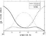
도 3은 본 발명의 일 실시예에 따른 유기전계발광소자의 점진 혼합 유기물 단일층의 깊이에 따른 유기물 비율.3 is an organic ratio according to the depth of the gradual mixed organic monolayer of the organic light emitting device according to an embodiment of the present invention.
도 4는 본 발명의 다른 일 실시예에 따른 유기전계발광소자의 점진 혼합 유기물 단일층의 깊이에 따른 유기물 증착속도.4 is an organic material deposition rate according to the depth of the progressive mixed organic single layer of the organic light emitting device according to another embodiment of the present invention.
도 5는 본 발명의 다른 실시예에 따른 유기전계발광소자의 점진 혼합 유기물 단일층의 깊이에 따른 유기물 비율.5 is an organic ratio according to the depth of the progressive mixed organic monolayer of the organic light emitting device according to another embodiment of the present invention.
도 6은 본 발명에 따른 유기전계발광소자의 구조를 나타내는 단면도.6 is a cross-sectional view showing the structure of an organic light emitting display device according to the present invention;
*도면의 주요부분에 대한 부호의 설명** Explanation of symbols for main parts of drawings *
100: 기판 200: 양극100: substrate 200: anode
300: 점진 혼합 유기물 단일층300: Progressive Mixed Organics Monolayer
400: 음극400: cathode
본 발명은 유기전계발광소자에 관한 것으로, 특히 발광물질과 정공전달물질및 전자전달물질을 포함하는 유기전계발광소자에 관한 것이다.The present invention relates to an organic electroluminescent device, and more particularly to an organic electroluminescent device comprising a light emitting material, a hole transport material and an electron transport material.
최근 표시장치의 대형화에 따라 공간 점유가 적은 평면표시소자의 요구가 증대되고 있는데, 이러한 평면표시소자 중 하나로서 유기전계발광소자(Organic Electroluminescence Device')의 기술이 빠른 속도로 발전하고 있다.Recently, as the size of the display device increases, the demand for a flat display device having less space is increasing. As one of the flat display devices, the technology of the organic electroluminescence device (Organic Electroluminescence Device ') is rapidly developing.
상기 유기전계발광소자는 ITO와 같은 투명전극인 양극과 일함수가 낮은 금속(Ca, Li, Al : Li, Mg : Ag 등)을 사용한 음극 사이에 유기 박막층이 있는 구조로 구성 되어 있으며, 이와 같은 유기전계발광소자에 순방향의 전압을 가하면 양극과 음극에서 각각 정공과 전자가 주입되고, 주입된 정공과 전자는 결합하여 엑시톤(exciton)을 형성하고, 엑시톤이 발광 재결합(radiative recombination)을 하게 되는데 이를 전기발광 현상이라 한다.The organic light emitting device is composed of a structure having an organic thin film layer between the anode, which is a transparent electrode such as ITO, and the cathode using a metal having a low work function (Ca, Li, Al: Li, Mg: Ag, etc.). When a forward voltage is applied to the organic light emitting diode, holes and electrons are injected from the anode and the cathode, respectively, and the injected holes and electrons combine to form an exciton, and the exciton undergoes radiative recombination. It is called electroluminescence phenomenon.
여기서, 상기 유기 박막층의 재료는 저분자 또는 고분자 물질로 구분할 수 있으며 저분자 물질은 진공 증착법을 사용하고, 고분자 물질은 스핀 코팅 방법으로 기판 상에 박막을 형성하며, 낮은 전압에서 소자를 동작시키기 위해 유기 박막층의 두께는 약 1000Å 정도로 매우 얇게 제작하는데, 박막이 균일하며 핀 홀(pin hole)과 같은 결함이 없어야 한다.Here, the material of the organic thin film layer may be classified into a low molecular weight or a polymer material, the low molecular material uses a vacuum deposition method, the polymer material forms a thin film on the substrate by a spin coating method, the organic thin film layer to operate the device at a low voltage The thickness of is made very thin, about 1000Å, the film should be uniform and free from defects such as pin holes.
또한, 이러한 상기 유기 박막층은 일반적으로 여러 유기물질의 다층 구조를 주로 사용한다. 유기전계발광소자를 다층 박막 구조로 제작하는 이유는 유기 물질의 경우 정공과 전자의 이동도가 크게 차이가 나므로 정공 전달층(HTL)과 전자 전달층(ETL)을 별도로 사용하면 정공과 전자가 유기 발광층(EML)으로 효과적으로 전달될 수 있기 때문이다.In addition, the organic thin film layer generally uses a multilayer structure of various organic materials. The reason why the organic light emitting device is manufactured in a multi-layered thin film structure is that the mobility of holes and electrons in organic materials varies greatly. Therefore, when the hole transport layer (HTL) and the electron transport layer (ETL) are used separately, holes and electrons are organic. This is because it can be effectively delivered to the light emitting layer (EML).
그러나 상기와 같은 종래의 다층구조의 유기전계발광소자에서는 엑시톤이 주로 유기 발광층과 정공 전달층의 계면 부근에 형성되어 확산하면서 발광하는 문제점을 가지고 있다.However, in the conventional organic EL device having a multilayer structure as described above, excitons are mainly formed in the vicinity of an interface between the organic light emitting layer and the hole transport layer and have a problem of emitting light while diffusing.
최근에는 다층구조의 유기전계발광소자에서 Alq3로 구성된 발광층과 TPD로 구성된 정공전달층 사이에 Alq3와 TPD의 균일 혼합물층을 더 포함시킴으로써 유기 EL의 양자효율을 더 높이려는 시도가 있었다(T. Mori et al. J. Phys. D: Appl. Phys. 32, L65(1999)). 또한, 더 나아가 Alq3로 구성된 발광층과 NPB로 구성된 정공전달층 사이에 Alq3와 NPB의 계단형 점진 혼합물층을 더 포함시키면 균일 혼합물층을 포함시킨 것보다 양자효율을 더욱 높일 수 있다는 연구 결과가 발표된 바도 있다(D. Ma et al. Appl. Phys. Lett. 80, 3641(2002)).Recently, further comprising a light-emitting layer and the TPD Alq3 and TPD uniform mixture layer between the hole transport layer consisting of consisting of Alq3 in the organic EL device of a multilayer structure by there was an attempt to further increase the quantum efficiency of the organic EL (T Mori et al. J. Phys. D: Appl. Phys. 32, L65 (1999). In addition, further research results that if further comprises a light-emitting layer and the NPB Alq3 and NPB stepped gradual mixture layer between the hole transport layer consisting of consisting of Alq3 than those that contain a uniform mixture layer can further increase the quantum efficiency It has also been published (D. Ma et al. Appl. Phys. Lett. 80, 3641 (2002)).
그러나 상기 유기 전계발광소자들은 모두 발광층과 정공전달층을 그대로 포함한 채 그 계면에 혼합물층을 더 포함하고 있어 다층구조의 한계를 벗어나지 못하고 있다. 이러한 다층구조에서는 계면이 존재할 수 밖에 없고 이러한 계면에서는 계면영역확산과 계면트랩준위가 전자 및 정공의 주입을 방해하는 문제점이 있다.However, all of the organic electroluminescent devices include a mixture layer at the interface while including the light emitting layer and the hole transport layer as it is, so as not to escape the limitation of the multilayer structure. In such a multi-layered structure, there must be an interface, and at this interface, the interface area diffusion and the interface trap level interfere with the injection of electrons and holes.
따라서, 유기물 단일층으로 구성됨으로써 엑시톤의 형성영역이 다층구조를 사용한 유기전계발광소자에 비해 상대적으로 넓고 계면이 존재하지 않으며 엑시톤 형성 효율 및 내부양자효율이 개선된 유기전계발광소자 및 그 제조방법에 대한 요구가 있다.Therefore, the organic electroluminescent device having an exciton forming region is relatively wider than the organic electroluminescent device using a multilayer structure and has no interface, and has improved exciton formation efficiency and internal quantum efficiency by being composed of an organic single layer. There is a demand.
본 발명은 상기와 같은 문제점을 해결하기 위한 것으로 발광층, 전자전달층, 정공전달층 등이 별도로 구성된 다층구조의 유기전계발광소자가 아닌 단일층으로 구성된 유기전계발광소자를 제공한다.The present invention is to solve the above problems and provides an organic electroluminescent device composed of a single layer instead of a multi-layer organic electroluminescent device having a light emitting layer, an electron transport layer, a hole transport layer and the like.
본 발명의 다른 면에서는 단일층으로 구성되고 양자효율이 높은 유기전계발광소자의 제조방법이 제공된다.In another aspect of the present invention, there is provided a method of manufacturing an organic light emitting display device having a single layer and having high quantum efficiency.
상기와 같은 목적을 달성하기 위하여 본 발명은 점진 혼합 유기물 단일층으로 구성된 유기전계발광소자를 제공한다.In order to achieve the above object, the present invention provides an organic electroluminescent device composed of a gradual mixed organic single layer.
도 1은 종래의 다층구조의 유기전계발광소자의 구조를 나타내는 단면도이다. 도 1을 참조하면, 종래의 유기전계발광소자는 기판(1), 제 1전극(2), 정공 주입층(3), 정공 전달층(4), 유기 발광층(5), 전자 전달층(6), 전자 주입층(7) 및 제 2전극(8)이 포함된다.1 is a cross-sectional view showing the structure of a conventional organic light emitting display device having a multilayer structure. Referring to FIG. 1, a conventional organic light emitting display device includes a
여기서, 상기 제 2전극(cathode)(8)은 작은 일함수를 갖는 금속인 Ca, Mg, Al 등이 쓰이고, 이는 상기 전극(8)과 유기 발광층(5) 사이에 형성되는 장벽(barrier)을 낮춤으로써 전자 주입에 있어 높은 전류 밀도(current density)를 얻을 수 있기 때문이며, 이를 통해 소자의 발광효율을 증가시킬 수 있게 된다.Here, the second electrode (cathode) 8 is a metal having a small work function of Ca, Mg, Al, etc. are used, which is a barrier (barrier) formed between the electrode (8) and the organic light emitting layer (5) This is because the lower the high current density in the electron injection can be obtained, thereby increasing the luminous efficiency of the device.
한편, 상기 제 1전극(anode)(2)은 정공 주입을 위한 전극으로 일함수가 높고 발광된 빛이 소자 밖으로 나올 수 있도록 투명 금속 산화물을 사용하며, 가장 널리 사용되는 정공 주입 전극으로는 ITO(indium tin oxide)로써, 두께는 약 100nm정도 이다.On the other hand, the first electrode (anode) (2) is a hole injection electrode using a transparent metal oxide so that the work function is high and the emitted light can come out of the device, the most widely used hole injection electrode ITO ( indium tin oxide) and its thickness is about 100 nm.
또한, 유기 발광층(5)은 상기 제 1, 2전극(2, 8)에서 각기 주입된 정공과 전자가 결합하여 형성된 엑시톤이 기저상태로 떨어지면서 빛이 발광되는 층으로, 재료로 Alq3, DPVBi 등의 저분자 유기물질들이 쓰인다.In addition, the organic
또한, 정공 주입층(3) 및 정공 전달층(4), 전자 전달층(6) 및 전자 주입층(7)은 각각 정공 및 전자의 이동도를 높이기 위하여 각각 제 1전극(2)과 유기 발광층(5) 사이 및 제 2전극(8)과 유기 발광층(5) 사이에 개재되어 형성되는 것이며, 이러한 상기 각 층들은 저분자 또는 고분자 유기 물질로 이루어 지며 상기 수송층의 조합을 통해 양자효율을 높이고, 캐리어(전자 또는 정공)들이 직접 주입되지 않고 수송층 통과의 2단계 주입과정을 통해 구동전압을 낮출 수 있으며, 또한, 상기 유기 발광층(5)에 주입된 전자와 정공이 유기 발광층(5)을 거쳐 반대편 전극으로 이동시 반대편 수송층에 막힘으로써 재결합 조절이 가능하여, 이를 통해 발광효율을 향상 시킬 수 있는 것이다.In addition, the
그러나 상기와 같은 다층구조의 유기전계발광소자에서 엑시톤은 발광층과 정 공전달층의 계면부근에 형성되어 확산하면서 발광하는 문제점이 있다. 상기 계면에서 존재하는 트랩 때문에 전자 및 정공의 주입 효율이 감소하고 이로인해 엑시톤의 형성 확률이 감소한다.However, in the organic electroluminescent device of the multilayer structure as described above, the exciton is formed in the vicinity of the interface between the light emitting layer and the hole transport layer has a problem of emitting light while diffusing. Because of the traps present at the interface, the injection efficiency of electrons and holes is reduced, thereby reducing the probability of formation of excitons.
따라서 본 발명에 따른 유기전계발광소자는 이러한 문제점을 해결하고 내부양자효율을 증진하는데 중대한 변수로 작용하는 엑시톤 형성 확률을 최대로 높일 수 있도록 정공전달물질, 발광물질 및 전자전달물질이 두께별로 다른 비율로 혼합되어 있는 점진 혼합 유기물 단일층을 포함한다.Therefore, in the organic light emitting device according to the present invention, the hole transporting material, the light emitting material, and the electron transporting material have different ratios depending on the thickness so as to maximize the probability of forming excitons, which acts as a critical parameter in solving these problems and enhancing the internal quantum efficiency. It comprises a progressive mixed organic monolayer which is mixed with.
상기 점진 혼합 유기물 단일층은 바람직하게는 상기 정공 전달물질, 발광물질 및 전자전달 물질을 동시에 증착하되 증착이 진행됨에 따라 증착속도를 조절함으로써 제조된다.The progressive mixed organic monolayer is preferably prepared by simultaneously depositing the hole transport material, the light emitting material and the electron transport material, and controlling the deposition rate as the deposition proceeds.
상기 점진 혼합 유기물 단일층은 양극 및 음극 사이에 개재되며, 상기 점진 혼합 유기물 단일층 제조시 바람직하게는 상기 정공전달물질의 증착속도는 양극에서 음극방향의 상기 유기물 단일층의 두께에 따라 감소하며, 상기 발광물질의 증착속도는 상기 유기물 단일층의 두께에 따라 증가하다가 감소하되, 그 최대치가 40 내지 60%의 두께가 되었을 때 발생하며, 상기 전자전달물질의 증착속도는 양극전극에서 음극전극방향의 상기 유기물 단일층의 두께에 따라 증가한다.The gradual mixed organic monolayer is interposed between the anode and the cathode, preferably in the preparation of the gradual mixed organic monolayer, the deposition rate of the hole transport material is reduced in accordance with the thickness of the organic monolayer from the anode to the cathode, The deposition rate of the light emitting material increases and decreases with the thickness of the organic single layer, but occurs when the maximum value is 40 to 60%. The deposition rate of the electron transporting material is from the anode electrode to the cathode electrode. It increases with the thickness of the organic monolayer.
상기 점진 혼합 유기물 단일층의 두께별 구간에 따른 혼합비는 바람직하게는 양극에서 음극방향으로 두께 20%이하 구간에서 상기 정공전달물질이 80중량%이상이고, 상기 발광물질 및 상기 전자전달물질이 각각 10중량%이하이고, 두께 20 내지 40% 구간에서 상기 정공전달물질이 35 내지 45중량%, 상기 발광물질이 35 내지 55 중량%, 상기 전자전달물질이 10 내지 20중량%이다. 그리고 두께 40 내지 60%구간에서, 상기 정공전달물질이 10 내지 20중량%, 상기 발광물질이 60 내지 80중량%, 상기 전자전달물질이 10 내지 20중량%이고, 두께 60 내지 80%구간에서 상기 전자전달물질이 35 내지 45중량%, 상기 발광물질이 35 내지 55중량%, 상기 정공전달물질이 10 내지 20중량%이다. 80%이상의 두께에서는 상기 전자전달물질이 80중량%이상이고, 상기 발광물질 및 상기 정공전달물질이 각각 10중량%이하인 것이 바람직하다.The mixing ratio according to the thickness-wise section of the progressive mixed organic material single layer is preferably 80% by weight or more of the hole transport material in a section of 20% or less in thickness from the anode to the cathode, and the light emitting material and the electron transporting material are each 10 It is less than the weight percent, 35 to 45% by weight of the hole transport material, 35 to 55% by weight of the light emitting material, 10 to 20% by weight of the electron transport material in the 20 to 40% thickness section. And 40 to 60% thickness, the hole transport material is 10 to 20% by weight, the light emitting material is 60 to 80% by weight, the electron transport material is 10 to 20% by weight, and the thickness is 60 to 80%. The electron transport material is 35 to 45% by weight, the light emitting material is 35 to 55% by weight, and the hole transport material is 10 to 20% by weight. When the thickness is 80% or more, the electron transport material is 80% by weight or more, and the light emitting material and the hole transport material are preferably 10% by weight or less.
본 발명에 따른 점진 혼합 유기물 혼합층은 상기 정공전달물질, 발광물질 및 전자전달물질 외에 정공차단물질을 더 포함할 수 있으며 상기 네 물질의 증착속도를 조절하여 점진 혼합 유기물 단일층을 형성할 수 있다.The progressive mixed organic material mixed layer according to the present invention may further include a hole blocking material in addition to the hole transport material, the light emitting material and the electron transport material, and may form a progressive mixed organic material single layer by controlling the deposition rates of the four materials.
이 경우, 상기 발광물질의 증착속도는 양극전극에서 음극전극방향의 상기 유기물 단일층의 두께에 따라 증가하다가 감소하되, 그 최대치가 40 내지 60%의 두께가 되었을 때 발생하며, 상기 정공차단물질의 증착속도는 상기 유기물 단일층의 두께 30 내지 50%구간에서 시작하여 두께에 따라 증가하다가 감소하되, 그 최대치가 70 내지 80%의 두께가 되었을 때 발생하되, 양극전극에서 음극전극방향의 상기 유기물 단일층의 두께에 따라 상기 전자전달물질의 증착속도는 증가하고, 상기 정공전달물질의 증착속도는 감소하는 것이 바람직하다.In this case, the deposition rate of the light emitting material increases and decreases according to the thickness of the organic single layer in the direction of the cathode electrode in the anode electrode, and decreases, and occurs when the maximum value is 40 to 60% of the thickness of the hole blocking material. The deposition rate starts at 30 to 50% of the thickness of the organic monolayer and increases with thickness and then decreases, but occurs when the maximum is 70 to 80% of the thickness of the organic monolayer. The deposition rate of the electron transport material increases and the deposition rate of the hole transport material decreases according to the thickness of the layer.
정공전달물질, 발광물질 및 전자전달물질 외에 정공차단물질을 더 포함하는 점진 혼합 유기물 단일층의 두께 구간에 따른 혼합비는 바람직하게는 양극에서 음극방향으로 두께 20%이하 구간에서 상기 정공전달물질이 80중량%이상이고 상기 발광물질 및 상기 전자전달물질이 각각 10중량%이하이고, 두께 20 내지 40% 구간에서 상기 정공전달물질이 35 내지 45중량%, 상기 발광물질이 35 내지 55중량%, 상기 전자전달물질이 10 내지 20중량%이고, 두께 40 내지 60%구간에서 상기 정공전달물질이 5 내지 15중량%, 상기 발광물질이 55 내지 85중량%, 상기 전자전달물질이 5 내지 15중량%, 상기 정공차단물질이 5 내지 15중량%이고, 두께 60 내지 80%구간에서 상기 전자전달물질이 11 내지 25중량%, 상기 발광물질이 11 내지 25중량%, 상기 정공전달물질이 3 내지 10중량%, 상기 정공차단물질이 40 내지 75중량%이고, 80%이상의 두께에서 상기 전자전달물질이 50 내지 80중량%, 상기 발광물질 및 상기 정공전달물질이 각각 10중량%이하, 상기 정공차단물질이 20 내지 30중량%인 것이 바람직하다. 상기 정공차단물질은 두께 40%이전에는 포함되지 않는 것이 바람직하다.The mixing ratio according to the thickness section of the progressively mixed organic material single layer further including a hole blocking material in addition to the hole transport material, the light emitting material and the electron transport material is preferably 80% or less in the section of 20% thickness from the anode direction to the cathode direction. More than 10% by weight and the light emitting material and the electron transporting material are each 10% by weight or less, 35 to 45% by weight of the hole transport material, 35 to 55% by weight of the light emitting material in the 20 to 40%
본 발명에 따른 유기전계발광소자의 점진 혼합 유기물 단일층의 두께는 100 내지 150nm인 것이 바람직하다. 상기 유기물 단일층의 두께가 100nm 이하이고 전극표면의 표면 거칠기가 동일한 경우 유기발광이 되는 동안 전자와 홀의 주입으로 인해 발생되는 주울열로 인해 발생되는 암점(dark spot)에 의해 유기발광소자의 수명이 더욱 단축되게 되며 150nm 이상의 두께인 경우 발광을 위해 넘어야할 문턱전압(threshold voltage)이 커지게 되는 단점이 있다. 따라서 10V 정도의 구동전압에서 안정적인 수명을 유기하기 위해 유기물층의 두께는 100 내지 150nm 의 두께로 성장하는게 가장 바람직하다.The thickness of the progressive mixed organic single layer of the organic light emitting device according to the present invention is preferably 100 to 150nm. When the thickness of the organic single layer is 100 nm or less and the surface roughness of the electrode surface is the same, the lifespan of the organic light emitting diode is increased due to the dark spot generated by Joule heat generated by the injection of electrons and holes during organic light emission. If the thickness is more shorter than 150 nm, there is a disadvantage in that a threshold voltage to be exceeded for light emission is increased. Therefore, in order to have a stable life at a driving voltage of about 10V, the thickness of the organic material layer is most preferably grown to a thickness of 100 to 150 nm.
본 발명은 단분자 유기발광소자에서 형광 또는 인광성 발광물질을 사용하는 경우의 구조에 적용되므로 정공전달물질로는 TPD 또는 NPB 를 사용하는 것이 바람 직하며 형광발광소자인 경우는 발광물질로 Alq3, DPVBi 등 또는 Alq3, DPVBi 등을 호스트 물질로 하여 DCM2, Ruburene 등의 게스트 물질을 혼합하여 사용할 수 있다. 인광발광소자인 경우는 Alq3 또는 CBP 의 호스트 물질에 PtOEP, Ir(ppy)3 등의 인광성 게스트 물질을 혼합하여 사용할 수 있고 인광성 발광소자인 경우 정공차단물질로 BCP 를 사용하는 것이 분자의 에너지 준위를 고려할 때 가장 바람직하다. 상기 유기발광소자의 전자전달물질로는 전자의 이동률이 가장 좋은 Alq3 를 사용하는게 가장 바람직하다.Since the present invention is applied to the structure of using a fluorescent or phosphorescent light emitting material in a monomolecular organic light emitting device, it is preferable to use TPD or NPB as the hole transport material, and in the case of a fluorescent light emitting device, Alq3 , DPVBi and the like, or Alq3 , DPVBi and the like can be used by mixing a guest material such as DCM2 , Ruburene. In the case of phosphorescent light emitting devices, phosphorescent guest materials such as PtOEP and Ir (ppy)3 can be mixed with Alq3 or CBP host material.In the case of phosphorescent light emitting devices, BCP is used as a hole blocking material. It is most desirable when considering the energy level. As the electron transporting material of the organic light emitting device, it is most preferable to use Alq3 having the best electron mobility.
이하, 첨부된 도면을 참조하여 본 발명의 바람직한 실시예를 보다 상세하게 설명하도록 한다.Hereinafter, exemplary embodiments of the present invention will be described in detail with reference to the accompanying drawings.
실시예 1Example 1
유리 기판 상부에 30Ω/□ 의 면저항을 갖는 ITO(Indium-tin Oxide)를 증착한다. 상기 ITO가 증착된 유리기판을 진공도 10-7Torr 인 유기분자증착기에 장착하고 정공전달물질, 발광물질 및 전자전달물질을 동시에 증착한다. 증착하는 동안 유기물층의 두께에 따라 각 물질의 증착속도를 도 2에 나타낸 것과 같이 조절한다. 유기물층의 두께가 얇을수록 증착초기의 증착속도이다. 도 2에 따르면 정공전달물질은 유기물 증착 초기에 가장 높은 증착속도를 나타내며 증착두께가 증가할수록 증착속도가 감소한다. 발광물질은 증착초기에 증착속도를 정지속도에서 점차 증가 시켜 유기물층 전체 두께의 50% 근방에서 최대의 증착속도를 가지고 이후 증착속도를 점차 감소시켜 증착한다. 마지막으로 전자전달물질은 정공전찰물질의 증착조절방법과 반대로 증착초기에 증착속도 0에서 점차 증착속도를 증가시켜 유기물증착이 끝나는 시점에서 최대의 증착속도를 갖도록 조절한다. 유기물 단일층의 전체 두께는 100 내지 150nm가 되도록 조절한다. 이와 같이 제조된 점진 혼합 유기물 단일층의 유기물층 두께에 따른 유기물 비율을 도 3에 도시하였다. 상기 점진 혼합 유기물 단일층위에 음극전극으로 Mg:Ag 또는 LiF/Al층을 증착하여 유기전계발광소자를 제작하였다. 그 구조는 도 6과 같다.Indium-tin oxide (ITO) having a sheet resistance of 30 mA /? Was deposited on the glass substrate. The ITO-deposited glass substrate is mounted on an organic molecular vapor deposition machine having a vacuum degree of 10-7 Torr, and simultaneously deposits a hole transport material, a light emitting material, and an electron transport material. During deposition, the deposition rate of each material is controlled as shown in FIG. 2 according to the thickness of the organic layer. The thinner the organic layer is, the faster the deposition rate is. According to FIG. 2, the hole transport material has the highest deposition rate at the beginning of organic material deposition, and the deposition rate decreases as the deposition thickness increases. The luminescent material is deposited at the initial deposition rate by gradually increasing the deposition rate from the stationary speed to the maximum deposition rate near 50% of the total thickness of the organic layer, and then gradually decreasing the deposition rate. Finally, the electron transport material is controlled to have the maximum deposition rate at the end of organic deposition by gradually increasing the deposition rate at the initial deposition rate of 0, as opposed to the deposition control method of the hole charge material. The overall thickness of the organic monolayer is adjusted to be 100 to 150 nm. The organic matter ratio according to the thickness of the organic material layer of the progressive mixed organic material monolayer thus prepared is illustrated in FIG. 3. An organic light emitting display device was fabricated by depositing an Mg: Ag or LiF / Al layer with a cathode electrode on the progressive mixed organic material single layer. The structure is shown in FIG.
상기와 같은 유기전계발광소자는 계면이 없어 내부양자효율이 증가하여 휘도가 높다.The organic light emitting diode as described above does not have an interface, so the internal quantum efficiency is increased, and thus the luminance is high.
실시예 2Example 2
유리 기판 상부에 30Ω/□ 의 면저항을 갖는 ITO(Indium-tin Oxide)를 증착한다. 상기 ITO가 증착된 유리기판을 진공도 10-7Torr 인 유기분자증착기에 장착하고 정공전달물질, 발광물질, 정공차단물질 및 전자전달물질을 동시에 증착한다. 증착하는 동안 유기물층의 두께에 따라 각 물질의 증착속도를 도 4에 나타낸 것과 같이 조절한다. 유기물층의 두께가 얇을수록 증착초기의 증착속도이다. 도 4에 따르면 정공전달물질은 유기물 증착 초기에 가장 높은 증착속도를 나타내며 유기물층의 증착두께가 증가할수록 증착속도가 감소한다. 발광물질은 증착초기에 증착속도를 정지속도에서 점차 증가시켜 유기물층 전체 두께의 50% 근방에서 최대의 증착속도를 가지고 이후 증착속도를 점차 감소시켜 증착한다. 정공차단물질도 발광물질과 동일한 방법으로 증착하지만 두께의 70% 근방에서 최대의 증착속도를 갖는다. 마지막으로 전자전달물질은 정공전달물질의 증착조절방법과 반대로 증착초기에 증착속도 0에서 점차 증착속도를 증가시켜 유기물증착이 끝나는 시점에서 최대의 증착속도를 갖도록 조절한다. 유기물 단일층의 전체 두께는 100 내지 150nm가 되도록 조절한다. 이와 같이 제조된 점진 혼합 유기물 단일층의 유기물층 두께에 따른 유기물 비율을 도 5에 도시하였다. 상기 점진 혼합 유기물 단일층위에 음극전극으로 Mg:Ag 또는 Al층을 증착하여 유기전계발광소자를 제작하였다.Indium-tin oxide (ITO) having a sheet resistance of 30 mA /? Was deposited on the glass substrate. The ITO-deposited glass substrate is mounted on an organic molecular vapor deposition machine having a vacuum degree of 10-7 Torr, and simultaneously deposits a hole transport material, a light emitting material, a hole blocking material, and an electron transport material. During the deposition, the deposition rate of each material is adjusted as shown in FIG. 4 according to the thickness of the organic layer. The thinner the organic layer is, the faster the deposition rate is. According to FIG. 4, the hole transport material has the highest deposition rate at the beginning of organic material deposition, and the deposition rate decreases as the deposition thickness of the organic material layer increases. The luminescent material is deposited at the initial deposition rate by gradually increasing the deposition rate from the stationary rate to have the maximum deposition rate near 50% of the total thickness of the organic layer, and then gradually decreasing the deposition rate. The hole blocking material is deposited in the same manner as the light emitting material, but has the maximum deposition rate in the vicinity of 70% of the thickness. Finally, the electron transfer material is controlled to have the maximum deposition rate at the end of organic deposition by gradually increasing the deposition rate at the initial deposition rate of 0 as opposed to the deposition control method of the hole transport material. The overall thickness of the organic monolayer is adjusted to be 100 to 150 nm. The organic matter ratio according to the organic material layer thickness of the progressive mixed organic material monolayer thus prepared is shown in FIG. 5. An organic light emitting display device was fabricated by depositing an Mg: Ag or Al layer with a cathode electrode on the progressive mixed organic material single layer.
상기와 같은 유기전계발광소자는 단일층으로 제조되어 계면이 없고 계단식 혼합이 아닌 점진혼합이므로 내부양자효율이 증가하여 휘도가 높다.Since the organic light emitting device as described above is manufactured in a single layer and has no interface and is gradually mixed instead of stepwise mixing, the internal quantum efficiency is increased and the luminance is high.
본 발명은 점진 혼합 유기물 단일층으로 구성된 고효율 단일층 유기전계발광소자를 사용하여 종래의 다층 구조의 유기 전계발광소자에서 문제시 되고 있는 효율저하의 요인을 제거하여 고효율 발광이 가능한 단일층을 갖는 새로운 구조의 유기전계발광소자를 제공한다. 단일층으로 형성된 유기발광소자는 다층구조의 계면영역에서 발생하는 트랩현상으로 인해 전자 및 정공의 주입효율이 떨어지는 것을 방지하여 주입효율이 높다. 또한 엑시톤의 형성지역이 넓어져 내부양자효율이 향상되는 우수한 효과가 있으며 정보 전자 통신분야에서 매우 유용한 발명이다.The present invention uses a high-efficiency single-layer organic electroluminescent device composed of a gradual mixed organic monolayer to remove the problem of efficiency degradation that is a problem in the conventional multi-layer organic electroluminescent device having a single layer capable of high efficiency light emission. An organic electroluminescent device having a structure is provided. The organic light emitting diode formed of a single layer has a high injection efficiency by preventing the injection efficiency of electrons and holes from dropping due to the trap phenomenon occurring in the interface region of the multilayer structure. In addition, the exciton formation area is wider, the internal quantum efficiency is improved, and is a very useful invention in the field of information and electronic communication.
Claims (11)
Translated fromKoreanPriority Applications (1)
| Application Number | Priority Date | Filing Date | Title |
|---|---|---|---|
| KR1020050054018AKR100665700B1 (en) | 2005-06-22 | 2005-06-22 | Manufacturing method of organic light emitting device |
Applications Claiming Priority (1)
| Application Number | Priority Date | Filing Date | Title |
|---|---|---|---|
| KR1020050054018AKR100665700B1 (en) | 2005-06-22 | 2005-06-22 | Manufacturing method of organic light emitting device |
Publications (2)
| Publication Number | Publication Date |
|---|---|
| KR20060134382A KR20060134382A (en) | 2006-12-28 |
| KR100665700B1true KR100665700B1 (en) | 2007-01-09 |
Family
ID=37812767
Family Applications (1)
| Application Number | Title | Priority Date | Filing Date |
|---|---|---|---|
| KR1020050054018AExpired - Fee RelatedKR100665700B1 (en) | 2005-06-22 | 2005-06-22 | Manufacturing method of organic light emitting device |
Country Status (1)
| Country | Link |
|---|---|
| KR (1) | KR100665700B1 (en) |
Families Citing this family (1)
| Publication number | Priority date | Publication date | Assignee | Title |
|---|---|---|---|---|
| KR101830790B1 (en) | 2011-06-30 | 2018-04-05 | 삼성디스플레이 주식회사 | Organic light-emitting diode and flat display device comprising the same |
- 2005
- 2005-06-22KRKR1020050054018Apatent/KR100665700B1/ennot_activeExpired - Fee Related
Also Published As
| Publication number | Publication date |
|---|---|
| KR20060134382A (en) | 2006-12-28 |
Similar Documents
| Publication | Publication Date | Title |
|---|---|---|
| JP3695714B2 (en) | Light emitting device with organic layer | |
| TWI389596B (en) | Organic electroluminescent device and method for preparing the same | |
| JP4024754B2 (en) | Light emitting device having organic layer | |
| TWI406440B (en) | An organic light emitting device with a plurality of organic electroluminescent units stacked upon each other | |
| KR101846410B1 (en) | Organic light emitting diode display | |
| JP4625911B2 (en) | Organic light emitting diode (OLED) | |
| US20060181199A1 (en) | Organic light emitting device comprising multilayer cathode | |
| CN102024908A (en) | Organic light emitting device and manufacturing method thereof | |
| CN1421115A (en) | High efficiency transparent organic light emitting devices | |
| JP2009060012A (en) | ORGANIC ELECTROLUMINESCENT ELEMENT, ITS MANUFACTURING METHOD, AND DISPLAY DEVICE | |
| TWI453967B (en) | Organic light-emitting device including transparent conducting oxide layer as cathode and method of manufacturing the same | |
| KR100811996B1 (en) | Organic electroluminescent device and organic electroluminescent display using same | |
| CN103715360A (en) | Organic electroluminescent device and display device | |
| KR20130000218A (en) | Electrode including magnetic material and organic light emitting device using the electrode | |
| KR101973207B1 (en) | Anode including metal oxides and an organic light emitting device having the anode | |
| CN106784354A (en) | Organic light emitting display and its manufacture method and organic light-emitting display device | |
| JP4615083B2 (en) | Organic electroluminescent device having double insulating layer | |
| KR100777099B1 (en) | High efficiency organic light emitting diodes and manufacturing method | |
| JP2006012821A (en) | Metal compounds for organic electronic devices-metal multilayer electrodes | |
| JP2002100474A (en) | Organic electroluminescence device | |
| KR101419809B1 (en) | Inverted organic light-emitting diode and display apparatus including the same | |
| JP2001093671A6 (en) | Organic electroluminescent device having double insulating layer | |
| WO2010128426A1 (en) | Electroluminescent device | |
| KR100888148B1 (en) | Organic electroluminescent device and manufacturing method thereof | |
| CN107968153B (en) | A kind of OLED device and preparation method |
Legal Events
| Date | Code | Title | Description |
|---|---|---|---|
| A201 | Request for examination | ||
| PA0109 | Patent application | St.27 status event code:A-0-1-A10-A12-nap-PA0109 | |
| PA0201 | Request for examination | St.27 status event code:A-1-2-D10-D11-exm-PA0201 | |
| E902 | Notification of reason for refusal | ||
| PE0902 | Notice of grounds for rejection | St.27 status event code:A-1-2-D10-D21-exm-PE0902 | |
| P11-X000 | Amendment of application requested | St.27 status event code:A-2-2-P10-P11-nap-X000 | |
| P13-X000 | Application amended | St.27 status event code:A-2-2-P10-P13-nap-X000 | |
| E701 | Decision to grant or registration of patent right | ||
| PE0701 | Decision of registration | St.27 status event code:A-1-2-D10-D22-exm-PE0701 | |
| PG1501 | Laying open of application | St.27 status event code:A-1-1-Q10-Q12-nap-PG1501 | |
| GRNT | Written decision to grant | ||
| PR0701 | Registration of establishment | St.27 status event code:A-2-4-F10-F11-exm-PR0701 | |
| PR1002 | Payment of registration fee | Fee payment year number:1 St.27 status event code:A-2-2-U10-U11-oth-PR1002 | |
| PG1601 | Publication of registration | St.27 status event code:A-4-4-Q10-Q13-nap-PG1601 | |
| R18-X000 | Changes to party contact information recorded | St.27 status event code:A-5-5-R10-R18-oth-X000 | |
| PR1001 | Payment of annual fee | Fee payment year number:4 St.27 status event code:A-4-4-U10-U11-oth-PR1001 | |
| PR1001 | Payment of annual fee | Fee payment year number:5 St.27 status event code:A-4-4-U10-U11-oth-PR1001 | |
| PR1001 | Payment of annual fee | Fee payment year number:6 St.27 status event code:A-4-4-U10-U11-oth-PR1001 | |
| FPAY | Annual fee payment | Payment date:20121011 Year of fee payment:7 | |
| PR1001 | Payment of annual fee | Fee payment year number:7 St.27 status event code:A-4-4-U10-U11-oth-PR1001 | |
| PN2301 | Change of applicant | St.27 status event code:A-5-5-R10-R11-asn-PN2301 | |
| PN2301 | Change of applicant | St.27 status event code:A-5-5-R10-R14-asn-PN2301 | |
| FPAY | Annual fee payment | Payment date:20131128 Year of fee payment:8 | |
| PR1001 | Payment of annual fee | Fee payment year number:8 St.27 status event code:A-4-4-U10-U11-oth-PR1001 | |
| R18-X000 | Changes to party contact information recorded | St.27 status event code:A-5-5-R10-R18-oth-X000 | |
| LAPS | Lapse due to unpaid annual fee | ||
| PC1903 | Unpaid annual fee | Not in force date:20141230 Payment event data comment text:Termination Category : DEFAULT_OF_REGISTRATION_FEE St.27 status event code:A-4-4-U10-U13-oth-PC1903 | |
| R18-X000 | Changes to party contact information recorded | St.27 status event code:A-5-5-R10-R18-oth-X000 | |
| PC1903 | Unpaid annual fee | Ip right cessation event data comment text:Termination Category : DEFAULT_OF_REGISTRATION_FEE Not in force date:20141230 St.27 status event code:N-4-6-H10-H13-oth-PC1903 | |
| P22-X000 | Classification modified | St.27 status event code:A-4-4-P10-P22-nap-X000 | |
| P22-X000 | Classification modified | St.27 status event code:A-4-4-P10-P22-nap-X000 | |
| R18-X000 | Changes to party contact information recorded | St.27 status event code:A-5-5-R10-R18-oth-X000 | |
| R18-X000 | Changes to party contact information recorded | St.27 status event code:A-5-5-R10-R18-oth-X000 | |
| P22-X000 | Classification modified | St.27 status event code:A-4-4-P10-P22-nap-X000 | |
| P22-X000 | Classification modified | St.27 status event code:A-4-4-P10-P22-nap-X000 |