KR100662784B1 - Method of forming black matrix of liquid crystal display device - Google Patents
Method of forming black matrix of liquid crystal display deviceDownload PDFInfo
- Publication number
- KR100662784B1 KR100662784B1KR1020040030763AKR20040030763AKR100662784B1KR 100662784 B1KR100662784 B1KR 100662784B1KR 1020040030763 AKR1020040030763 AKR 1020040030763AKR 20040030763 AKR20040030763 AKR 20040030763AKR 100662784 B1KR100662784 B1KR 100662784B1
- Authority
- KR
- South Korea
- Prior art keywords
- black matrix
- resin
- printing
- printing roll
- forming
- Prior art date
- Legal status (The legal status is an assumption and is not a legal conclusion. Google has not performed a legal analysis and makes no representation as to the accuracy of the status listed.)
- Expired - Fee Related
Links
Images


Classifications
- E—FIXED CONSTRUCTIONS
- E02—HYDRAULIC ENGINEERING; FOUNDATIONS; SOIL SHIFTING
- E02D—FOUNDATIONS; EXCAVATIONS; EMBANKMENTS; UNDERGROUND OR UNDERWATER STRUCTURES
- E02D3/00—Improving or preserving soil or rock, e.g. preserving permafrost soil
- E02D3/02—Improving by compacting
- E02D3/10—Improving by compacting by watering, draining, de-aerating or blasting, e.g. by installing sand or wick drains
- B—PERFORMING OPERATIONS; TRANSPORTING
- B41—PRINTING; LINING MACHINES; TYPEWRITERS; STAMPS
- B41M—PRINTING, DUPLICATING, MARKING, OR COPYING PROCESSES; COLOUR PRINTING
- B41M3/00—Printing processes to produce particular kinds of printed work, e.g. patterns
- B41M3/003—Printing processes to produce particular kinds of printed work, e.g. patterns on optical devices, e.g. lens elements; for the production of optical devices
- E—FIXED CONSTRUCTIONS
- E02—HYDRAULIC ENGINEERING; FOUNDATIONS; SOIL SHIFTING
- E02D—FOUNDATIONS; EXCAVATIONS; EMBANKMENTS; UNDERGROUND OR UNDERWATER STRUCTURES
- E02D2300/00—Materials
- E02D2300/0004—Synthetics
- E02D2300/0006—Plastics
- E—FIXED CONSTRUCTIONS
- E02—HYDRAULIC ENGINEERING; FOUNDATIONS; SOIL SHIFTING
- E02D—FOUNDATIONS; EXCAVATIONS; EMBANKMENTS; UNDERGROUND OR UNDERWATER STRUCTURES
- E02D2600/00—Miscellaneous
- E02D2600/20—Miscellaneous comprising details of connection between elements
Landscapes
- Engineering & Computer Science (AREA)
- Structural Engineering (AREA)
- Manufacturing & Machinery (AREA)
- Life Sciences & Earth Sciences (AREA)
- General Life Sciences & Earth Sciences (AREA)
- Soil Sciences (AREA)
- Environmental & Geological Engineering (AREA)
- Mining & Mineral Resources (AREA)
- Paleontology (AREA)
- Civil Engineering (AREA)
- General Engineering & Computer Science (AREA)
- Agronomy & Crop Science (AREA)
- Liquid Crystal (AREA)
- Optical Filters (AREA)
Abstract
Translated fromKoreanDescription
Translated fromKorean도1은 일반적인 액정표시소자의 단면도.1 is a cross-sectional view of a general liquid crystal display device.
도2a∼도2f는 본 발명의 인쇄방식에 의한 블랙매트릭스 형성방법을 나타낸 도면.2A to 2F show a method of forming a black matrix by the printing method of the present invention.
도3a∼도3c는 인쇄방식에 의한 블랙매트릭스 형성방법의 다른 예를 나타낸 도면.3A to 3C are views showing another example of the black matrix forming method by the printing method.
도4a∼도4c는 인쇄방식에 의한 블랙매트릭스 형성방법의 또 다른 예를 나타낸 도면.4A to 4C are diagrams showing still another example of the black matrix forming method by the printing method.
도5는 본 발명의 인쇄방식에 의해 형성된 블랙매트릭스를 나타낸 단면도.5 is a cross-sectional view showing a black matrix formed by the printing method of the present invention.
도6은 칼라필터 하부에 형성된 블랙매트릭스를 나타낸 단면도.6 is a cross-sectional view showing a black matrix formed under the color filter.
도7은 칼라필터 상부에 형성된 블랙매트릭스를 타나낸 단면도.Figure 7 is a cross-sectional view showing a black matrix formed on the top of the color filter.
*** 도면의 주요부분에 대한 부호의 설명 ****** Explanation of symbols for main parts of drawing ***
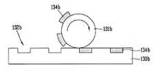
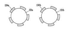
131a,231a,331a: 제1인쇄롤131a, 231a, 331a: first printing roll
131b,231b,331b: 제2인쇄롤131b, 231b, 331b: second printing roll
134',234',334',434': 블랙매트릭스134 ', 234', 334 ', 434': Black Matrix
140,240,340,440: 기판140,240,340,440: substrate
450: 칼라필터450: color filter
본 발명은 액정표시소자에 관한 것으로, 특히 인쇄방식의한 액정표시소자의 블랙매트릭스 형성방법에 관한 것이다.The present invention relates to a liquid crystal display device, and more particularly, to a method of forming a black matrix of a liquid crystal display device by a printing method.
근래, 핸드폰(Mobile Phone), PDA, 노트북컴퓨터와 같은 각종 휴대용 전자기기가 발전함에 따라 이에 적용할 수 있는 경박단소용의 평판표시장비(Flat Panel Display Device)에 대한 요구가 점차 증대되고 있다. 이러한 평판표시장비로는 LCD(Liquid Crystal Display), PDP(Plasma Display Panel), FED(Field Emission Display), VFD(Vacuum Fluorescent Display) 등이 활발히 연구되고 있지만, 양산화 기술, 구동수단의 용이성, 고화질의 구현이라는 이유로 인해 현재에는 액정표시소자(LCD)가 각광을 받고 있다.Recently, with the development of various portable electronic devices such as mobile phones, PDAs, and notebook computers, there is an increasing demand for flat panel display devices for light and thin applications. Such flat panel displays are being actively researched, such as LCD (Liquid Crystal Display), PDP (Plasma Display Panel), FED (Field Emission Display), VFD (Vacuum Fluorescent Display), but mass production technology, ease of driving means, Liquid crystal display devices (LCDs) are in the spotlight for reasons of implementation.
도 1은 일반적인 액정표시소자의 단면을 개략적으로 나타낸 것이다. 도면에 도시된 바와 같이, 액정표시소자(1)는 하부기판(5)과 상부기판(3) 및 상기 하부기판(5)과 상부기판(3) 사이에 형성된 액정층(7)으로 구성되어 있다. 하부기판(5)은 구동소자 어레이(Array)기판으로써, 도면에는 도시하지 않았지만, 상기 하부기판(5)에는 복수의 화소가 형성되어 있으며, 각각의 화소에는 박막트랜지스터(Thin Film Transistor)와 같은 구동소자가 형성되어 있다. 상부기판(3)은 칼라필터(Color Filter)기판으로써, 실제 칼라를 구현하기 위한 칼라필터 층과 빛샘을 차단하기 위한 블랙매트릭스이 형성되어 있다. 또한, 상기 하부기판(5) 및 상부기판(3)에는 각각 화소전극 및 공통전극이 형성되어 있으며 액정층(7)의 액정분자를 배향하기 위한 배향막(미도시)이 도포되어 있다.1 schematically illustrates a cross section of a general liquid crystal display device. As shown in the figure, the liquid
상기 하부기판(5) 및 상부기판(3)은 실링재(Sealing material;9)에 의해 합착되어 있으며, 그 사이에 액정층(7)이 형성되어 상기 하부기판(5)에 형성된 구동소자에 의해 액정분자를 구동하여 액정층을 투과하는 광량을 제어함으로써 정보를 표시하게 된다.The
상기 하부기판(5)은 하부기판(5)에 구동소자를 형성하는 구동소자 어레이기판공정에 의해서 형성되고, 상기 상부기판(3)은 칼라필터를 형성하는 칼라필터기판공정에 의해서 형성된다.The
구동소자 어레이기판공정은 하부기판(5)상에 배열되어 화소영역을 정의하는 복수의 게이트라인(Gate Line) 및 데이터라인(Date Line)을 형성하고 상기 화소영역 각각에 상기 게이트라인과 데이터라인에 접속되는 구동소자인 박막트랜지스터를 형성한 후, 박막트랜지스터에 접속되어 박막트랜지스터를 통해 신호가 인가됨에 따라 액정층을 구동하는 화소전극을 형성함으로써 이루어진다.In the driving device array substrate process, a plurality of gate lines and data lines are formed on the
또한, 칼라필터기판공정은 상부기판(3)에 블랙매트릭스를 형성한 후, 그 상부에 칼라필터를 형성한 다음, 공통전극을 형성함으로써 이루어진다.In addition, the color filter substrate process is performed by forming a black matrix on the
이때, 상기 블랙매트릭스는 Cr 또는 CrOx와 같은 반사특성이 우수한 금속막을 사용할 수 있으며, 광을 더욱 효과적으로 차단시키기 위해 2중막을 사용할 수도 있다. 그러나, 블랙매트릭스를 2중층으로 형성하는 경우, 1회의 포토리소그래피 공 정이 추가되는 문제가 발생하게 된다. 일반적으로 금속패턴으로 이루어지는 블랙매트릭스는 포토리소그래피방식을 통해 제작되는데, 포토리소그래피방식은 금속막 증착, 노광, 현상 및 스트립공정과 같이 복잡한 공정으로 이루어지는 것으로, 포토리소그래피 공정의 추가는 생산성을 저하시키는 요인이된다.In this case, the black matrix may use a metal film having excellent reflection characteristics such as Cr or CrOx, and may use a double film to block light more effectively. However, when the black matrix is formed in two layers, a problem arises in that one photolithography process is added. In general, black matrices made of metal patterns are fabricated through photolithography. Photolithography is a complex process such as metal film deposition, exposure, development, and stripping. The addition of a photolithography process lowers productivity. Become.
한편, 금속막에 대신에 수지BM을 적용할 수도 있다 수지BM은 재료 특성상 금속막에 비해 두께가 두껍기 때문에 광을 효과적으로 차단할 수가 있다. 즉, 수지BM은 스핀코터장비를 사용하기 때문에 두께를 줄이는데 한계가 있다. 그러나, 수지BM의 두께가 두꺼워짐에 따라 단차발생이 심화되며, 이를 해결하기 하기 위해 오버코트막(overcoat layer)을 형성하거나, 수지BM 형성이후, 그 표면을 제거하는 폴리싱 공정을 적용해야만 한다.On the other hand, resin BM may be applied instead of the metal film. Since the resin BM is thicker than the metal film due to the material properties, it is possible to effectively block light. That is, the resin BM has a limit in reducing the thickness because it uses a spin coater equipment. However, as the thickness of the resin BM becomes thicker, a step difference is intensified. In order to solve this problem, an overcoat layer is formed or a polishing process for removing the surface of the resin BM is removed.
이와 같이, 종래 블랙매트릭스 형성공정은 이중 금속막을 적용하는 경우, 포토마스크공정 추가되며, 수지BM을 적용하는 경우, 오버코트막 형성 또는 폴리싱공정이 추가되기 때문에 생산성이 저하되는 문제점이 있었다.As described above, the conventional black matrix forming process has a problem in that productivity is lowered when a double metal film is applied, a photomask process is added, and when resin BM is applied, an overcoat film forming or polishing process is added.
따라서, 본 발명은 상기한 문제점을 해결하기 위해서 이루어진 것으로, 본 발명의 목적은 인쇄방식을 통해 블랙매트릭스를 형성함으로써, 공정을 단순화 및 생산성 향상을 꾀할 수 있는 액정표시소자의 블랙매트릭스 형성방법을 제공하는 것이다.Accordingly, the present invention has been made to solve the above problems, and an object of the present invention is to provide a method of forming a black matrix of a liquid crystal display device which can simplify the process and improve productivity by forming a black matrix through a printing method. It is.
또한, 본 발명의 다른 목적은 수지BM에 비해 상대적으로 두께가 얇은 블랙매트릭스를 다중층으로 인쇄함으로써, 광을 효과적으로 차단시킬 수 있는 액정표시소 자의 블랙매트릭스 형성방법을 제공하는 것이다.Another object of the present invention is to provide a method of forming a black matrix of a liquid crystal display device capable of effectively blocking light by printing a black matrix having a relatively thin thickness compared to resin BM in multiple layers.
기타 본 발명의 목적 및 특징은 이하의 발명의 구성 및 특허청구범위에서 상세히 기술될 것이다.Other objects and features of the present invention will be described in detail in the configuration and claims of the following invention.
상기와 같은 목적을 달성하기 위해 이루어지는 본 발명은 투명한 기판을 준비하는 단계와, 상기 기판 상에 제1블랙매트릭스를 인쇄하는 단계 및 상기 제1블랙매트릭스 상에 제2블랙매트릭스를 인쇄하는 단계를 포함하여 이루어지는 액정표시소자의 블랙매트릭스 형성방법을 제공한다.The present invention made to achieve the above object comprises the steps of preparing a transparent substrate, printing a first black matrix on the substrate and printing a second black matrix on the first black matrix. A black matrix forming method of a liquid crystal display device is provided.
상기 제1블랙매트릭스를 인쇄하는 단계는 복수의 홈이 형성된 제1클리체를 준비하는 단계와, 상기 홈 내부에 수지BM을 충진하는 단계와, 상기 제1클리체 상에 제1인쇄롤를 접촉시킨 상태에서 이를 회전시킴에 따라 상기 홈 내부에 충진된 수지BM을 제1인쇄롤 표면에 전사시키는 단계 및 상기 제1인쇄롤 표면에 전사된 수지BM을 상기 기판 상에 전사시키는 단계로 이루어진다.The printing of the first black matrix may include preparing a first cliché formed with a plurality of grooves, filling a resin BM into the grooves, and contacting a first printing roll on the first cliché. As it rotates in a state, the resin BM filled in the grooves is transferred to the first printing roll surface, and the resin BM transferred to the first printing roll surface is transferred onto the substrate.
그리고, 상기 제2블랙매트릭스를 인쇄하는 단계는 복수의 홈이 형성된 제2클리체를 준비하는 단계와, 상기 홈 내부에 수지BM을 충진하는 단계와, 상기 제2클리체 상에 제2인쇄롤을 접촉시킨 상태에서 이를 회전시킴에 따라 홈 내부에 충진된 수지BM을 인쇄롤 표면에 전사시키는 단계 및 상기 제2인쇄롤 표면에 전사된 수지BM을 상기 제1블랙매트릭스 상에 전사시키는 단계로 이루어진다.The printing of the second black matrix may include preparing a second cliché formed with a plurality of grooves, filling a resin BM into the grooves, and printing a second printing roll on the second cliché. Transferring the resin BM filled in the groove to the surface of the printing roll by rotating the resin BM in the groove and transferring the resin BM transferred on the surface of the second printing roll onto the first black matrix. .
이때, 상기 제1 및 제2클리체는 롤 형상일 수도 있다. 즉, 상기 제1 및 제2클리체는 롤 형상으로 상기 제1 및 제2인쇄롤과 맞물려 회전하며, 상기 인쇄롤 표 면에 수지BM을 전사시키게 된다.In this case, the first and second cleats may have a roll shape. That is, the first and second cleats are rotated in engagement with the first and second printing rolls in a roll shape, and transfer the resin BM to the surface of the printing roll.
아울러, 상기 제1블랙매트릭스와 제2블랙매트릭스의 크기를 다르게 형성할 수 있으며, 특히, 상기 제1블랙매트릭스를 제2블랙매트릭스 보다 크게 형성할 수 있다.In addition, the sizes of the first black matrix and the second black matrix may be differently formed, and in particular, the first black matrix may be formed larger than the second black matrix.
또한, 광차단 특성을 더욱 향상시키기 위해 상기 제1블랙매트릭스 상에 나노입자층을 형성하는 단계를 더 포함하여 이루어질 수 있다.In addition, the method may further include forming a nanoparticle layer on the first black matrix to further improve light blocking properties.
또한, 본 발명은 제1 및 제2블랙매트릭스로 한정하지 않으며, 그 상부에 적어도 한층의 제3블랙매트릭스를 인쇄하는 단계를 더 포함할 수도 있다.In addition, the present invention is not limited to the first and second black matrices, and may further include printing at least one layer of the third black matrices thereon.
또한, 본 발명은 복수의 볼록패턴이 형성된 제1 및 제2인쇄롤을 준비하는 단계와, 상기 볼록패턴 표면에 수지BM을 도포하는 단계와, 상기 제1인쇄롤의 볼록패턴 표면에 도포된 잉크를 기판에 접촉시킨 상태에서 제1인쇄롤을 회전시킴에 따라 기판 상에 기판 상에 제1블랙매트릭스를 형성하는 단계 및 상기 제2인쇄롤의 볼록패턴 표면에 도포된 잉크를 기판 상에 형성된 제1블랙매트릭스에 접촉시킨 상태에서 제2인쇄롤을 회전시킴에 따라, 제1블랙매트릭스 상에 제2블랙매트리스를 형성하는 단계를 포함하여 이루어진다.In addition, the present invention comprises the steps of preparing a first and second printing roll having a plurality of convex patterns, coating the resin BM on the surface of the convex pattern, ink applied to the surface of the convex pattern of the first printing roll Forming a first black matrix on the substrate as the first printing roll is rotated in contact with the substrate, and the ink formed on the convex pattern surface of the second printing roll on the substrate. And rotating the second printing roll in contact with the first black matrix, thereby forming a second black mattress on the first black matrix.
그리고, 광차단 효율을 향상시키기 위해 상기 제1블랙매트릭스 상에 나노입자층을 추가로 형성할 수 있다.In addition, a nanoparticle layer may be further formed on the first black matrix to improve light blocking efficiency.
이하, 첨부한 도면을 통해 본 발명의 인쇄방식에 의한 액정표시소자의 블랙매트릭스 형성방법에 대해 상세히 설명하도록 한다.Hereinafter, the black matrix forming method of the liquid crystal display device according to the printing method of the present invention will be described in detail with reference to the accompanying drawings.
도2a∼도2f는 본 발명의 인쇄방식에 의한 블랙매트릭스 형성방법을 나타낸 것으로, 먼저, 도2a에 도시된 바와 같이, 인쇄방식에서는 우선 오목판 또는 제1클리체(130a)의 특정 위치에 제1홈(132a)을 형성한 후 상기 제1홈(132a) 내부에 수지BM(134)을 충진한다. 상기 제1클리체(130a)에 형성되는 제1홈(132a)은 일반적인 포토리소그래피방법에 의해 형성되며, 제2홈(132a) 내부로의 수지BM(134) 충진은 제1클리체(130a)의 상부에 BM형성용 수지(134)를 을 도포한 후 닥터블레이드(138)를 제1클리체(130a)의 표면에 접촉한 상태에서 밀어줌으로써 이루어진다. 따라서, 닥터블레이드(138)의 진행에 의해 제1홈(132a) 내부에 수지BM(134)이 충진됨과 동시에 제1클리체(130a) 표면에 남아 있는 수지BM(134)은 제거된다.2A to 2F illustrate a method of forming a black matrix according to the printing method of the present invention. First, as shown in FIG. 2A, in the printing method, first, at a specific position of the concave plate or the
이때, 상기 제1홈(132a)의 깊이는 형성하고자 하는 BM의 두께를 결정하는 것으로, 상대적으로 홈의 깊이가 얇을수록 두께가 얇은 BM을 형성할 수가 있다.At this time, the depth of the
도2b에 도시된 바와 같이, 상기 제1클리체(130a)의 제1홈(132a) 내부에 충진된 수지BM(134)은 제1클리체(130a)의 표면에 접촉하여 회전하는 제1인쇄롤(131a)의 표면에 전사되어 제1수지BM패턴(134a)를 형성한다. 상기 제1인쇄롤(131a)은 제작하고자 하는 표시소자의 패널의 폭과 유사한 폭으로 형성되며, 패널의 길이와 비슷한 길이의 원주를 갖는다. 따라서, 1회의 회전에 의해 제1클리체(130a)의 제1홈(132a)에 충진된 수지BM(134)이 모두 제1인쇄롤(131a)의 원주 표면에 전사되어 제1수지BM패턴(134a)를 형성한다.As shown in FIG. 2B, the
도2a 및 도2b의 제1인쇄롤(131a) 표면에 제1수지BM패턴(134a)을 형성하는 동안, 도2c 및 도2d에 도시된 바와 같이, 제2클리체(130b)를 준비한다. 그리고, 상기 제2클리체(130b)에 형성된 제2홈(132b) 내부에 수지BM(134)을 충진한 후, 상기 제2홈(132b) 내부에 충진된 수지BM(134)을 제2인쇄롤(131b) 표면에 전사시킴으로써, 도2e에 도시된 바와 같이, 제1수지BM패턴(134a)이 형성된 제1인쇄롤(131a)과 제2수지BM패턴(134b)이 형성된 제2인쇄롤(131b)을 각각 준비한다.While the first
이후, 도2f에 도시된 바와 같이, 상기 제1인쇄롤(131a)을 기판(130) 위에 접촉시킨 상태에서 회전시킴에 따라 제1인쇄롤(131a)에 전사된 제1수지BM패턴(134a)이 기판(130) 상에 전사되어, 기판(130) 상에 제1블랙매트릭스(134a')를 형성하게 된다. 이어서, 상기 제1블랙매트릭스(134a') 위에 제2인쇄롤(131b)을 접촉시킨 상태에서 회전시킴에 따라 상기 제1블랙매트릭스(134a') 상에 제2수지BM패턴(134b)을 전사시킴으로써, 제2블랙매트릭스(134b')를 형성하게 된다. 이때, 제1블랙매트릭스(134a')와 제2블랙매트릭스(134b') 사이에는 계면이 형성되며, 상기 계면이 광차단 효율을 향상시키는 역할을 한다. 즉, 상기 제1 및 제2블랙매트릭스(134a',134b')가 동일한 물질로 형성된다고 하더라고, 제1블랙매트릭스(134a')에 함유된 솔벤트가 모두 휘발된 후, 그 상부에 제2블랙매트릭스(134b')가 형성되기 때문에, 제1블랙매트릭스(134a')와 제2블랙매트릭스(134b') 사이에는 계면이 형성된다.Thereafter, as shown in FIG. 2F, the first
한편, 상기 기판(140) 상에 제1블랙매트릭스(134a')를 형성한 후, UV 또는 열을 인가함으로써, 솔벤트의 휴발성을 증진시킬 수가 있으며, 제2블랙매트릭스(134b')는 UV 또는 열공정을 끝낸 제1블랙매트릭스(134a') 상에 형성할 수 있다. 이와 같이, 제1블랙매트릭스(134a') 형성 후에 UV 또는 열을 인가함 으로써, 계면형성을 더욱 확실히 할 수 있다.On the other hand, after forming the first
또한, 상기 제1블랙매트릭스(134a')를 형성한 후, 그 상부에 나노입자층(미도시)을 형성할 수도 있다. 즉, 제1블랙매트릭스(134a')와 제2블랙매트릭스(134b') 사이에 나노입자층을 추가로 형성함으로써, 광차단 특성을 향상시킬 수가 있다. 나노입자층이 광투과율을 저하시킴으로써, 광을 효과적으로 차단할 수 있도록 한다.In addition, after forming the first
따라서, 본 발명에서는 블랙매트릭스의 두께를 키우지 않아도 광을 효과적으로 차단시킬 수가 있다. 즉, 클리체의 홈 깊이를 변경함으로써, 블랙매트릭스의 두께를 용이하게 조절할 수 있으며, BM수지를 이용하여 다층의 블랙매트릭스를 형성하기 때문에, 종래에 비해 광차단 효율을 증가시키는 동시에 BM두께를 줄일 수가 있다. 따라서, 굳이 오버코트막을 형성하지 않아도 되며, 인쇄방식을 통해 블랙매트릭스를 형성하기 때문에, 비록 다층BM을 형성하더라고, 종래에 비해 공정이 매우 단순하다.Therefore, in the present invention, light can be effectively blocked without increasing the thickness of the black matrix. That is, by changing the groove depth of the cliché, the thickness of the black matrix can be easily adjusted, and the multilayer black matrix is formed using the BM resin, thereby increasing the light blocking efficiency and reducing the BM thickness in comparison with the conventional method. There is a number. Therefore, it is not necessary to form the overcoat film, and since the black matrix is formed through the printing method, even if the multilayer BM is formed, the process is very simple as compared with the prior art.
한편, 상기 제1인쇄롤(131a)이 기판(130) 상에 제1블랙매트릭스(134a')를 형성할때, 제2인쇄롤(131b)은 상기 제1블랙매트릭스(134a') 상에 제2블랙매트릭스(134b')를 형성하기 때문에, 제1 및 제2인쇄롤(131a,131b)이 기판(130)을 지난 후에, 기판(130) 상에는 제1블랙매트릭(134a') 및 제2블랙매트릭스(134b')로 구성된 블랙매트릭스(134')가 형성된다. 이때, 상기 제1블랙매트릭스(134a') 상에 상기 제2블랙매트릭스(134b')는 정확하게 제1블랙매트릭스(134a') 상에 형성되어야 한다. 즉, 제1인쇄롤(131a)과 제2인쇄롤(131b)를 기판(130)과 정확하게 얼라인하여 제2블랙매트릭스(134b')가 제1블랙매트릭스(134b') 상에 형성되도록 해야 한다. 그러나, 실제 공정에서는 상기 제1 및 제2인쇄롤(131a,131b)의 얼라인 오차를 고려하여 상기 제1블랙매트릭스(134a')를 더 크게 형성할 수도 있다. 또한, 상기 제1블랙매트릭스(134a') 및 제2블랙매트릭스(134b')의 두께를 다르게 형성할 수도 있으며, 제1 및 제2블랙매트릭스(134a',134b')의 두께는 클리체의 홈두께에 의해 조절할 수 있다.Meanwhile, when the
이와 같이, 본 발명에서는 클리체에 형성되는 홈의 두께를 조절하여 블랙매트릭스의 두께를 결정할 수 있기 때문에, 수지BM을 사용하더라도, 종래에 비해 그 두께를 얇게 형성할 수가 있다. 따라서, 수지BM 사용시 오버코트막을 생략할 수도 있다.As described above, in the present invention, since the thickness of the grooves formed in the cliché can be adjusted to determine the thickness of the black matrix, even if resin BM is used, the thickness can be made thinner than in the prior art. Therefore, the overcoat film may be omitted when using resin BM.
한편, 본 발명은 클리체를 사용하지 않고, 인쇄롤 표면에 홈을 형성하고, 상기 홈 내부에 수지BM을 충진시킨 후, 이를 바로 기판 상에 인쇄할 수도 있다.On the other hand, in the present invention, the grooves are formed on the surface of the printing roll without the use of the cliché, and the resin BM is filled in the grooves, and this may be immediately printed on the substrate.
즉, 도3a에 도시된 바와 같이, 표면에 복수의 홈(232)이 형성된 인쇄롤(231)을 준비한 다음, 이를 수지BM(234)이 담긴 용기(220)에 소정영역 담근 상태에서 회전시키는 동시에, 그 표면을 닥터블레이드(238)로 밀어줌으로써, 홈(232) 내부에 수지BM(234)을 충진시킬 수가 있다. 이와 같이, 제1수지BM패턴(234a) 및 제2수지BM패턴(234b)이 각각 충진된 제1 및 제2인쇄롤(231a,231b)을 준비한 후(도3b), 도3c에 도시된 바와 같이, 상기 제1인쇄롤(231a)을 기판(240)에 접촉시킨 상태에서 회전함에 따라, 기판(240) 상에 제1수지BM패턴(234a)을 전사시킴으로써, 제1블랙매트릭스(234a')를 형성한다. 이어서, 제2인쇄롤(231b)을 통해 제1블랙매트릭스(234a') 상부에 제2블랙매트릭스(234b')를 형성할 수가 있다. 따라서, 인쇄롤 표면에 형성된 홈은 형성하고자 하는 블랙매트릭스의 패턴과 동일해야 한다.That is, as shown in Figure 3a, after preparing a
또한, 본 발명은 표면에 형성하고자하는 블랙매트릭스와 동일한 형태의 볼록패턴을 가지는 인쇄롤을 사용할 수도 있다.In addition, the present invention may use a printing roll having a convex pattern of the same shape as the black matrix to be formed on the surface.
즉, 도4a에 도시된 바와 같이, 형성하고자 하는 패턴과 동일한 형태의 볼록패턴(332)이 형성된 인쇄롤(331)을 준비하고, 상기 볼록패턴(332) 표면에 수지BM패턴(334)을 도포한다. 이때, 수지BM패턴(334)은 수지BM 공급롤(360)에 의해서 형성되며, 수지BM 공급롤(360)과 인쇄롤(331)이 맞물려 회전하면서 수지BM 공급기(335)에 의해 수지BM 공급롤(360) 표면에 제공된 수지BM(334)이 인쇄롤(331)의 볼록패턴(332)에 형성된다.That is, as shown in FIG. 4A, a
이와 같은 방법을 통해, 도4b에 도시된 바와 같이, 제1볼록패턴(332a) 표면에 제1수지BM패턴(334a)이 도포된 제1인쇄롤(331a)과 제2볼록패턴(332b) 표면에 제2수지BM패턴(334b)이 도포된 제2인쇄롤(331b)을 준비한다.Through the above method, as shown in FIG. 4B, the surface of the
이어서, 도4c에 도시된 바와 같이, 상기 제1인쇄롤(331a)을 기판(340)에 접촉시킨 상태에서 회전함에 따라, 기판(340) 상에 제1수지BM패턴(334a)을 전사시킴으로써, 제1블랙매트릭스(334a')를 형성한다. 이어서, 제2인쇄롤(331b)을 통해 제1블랙매트릭스(334a') 상부에 제2블랙매트릭스(334b')를 형성할 수가 있다. 따라서, 인쇄롤 표면에 형성된 볼록패턴은 블랙매트릭스의 패턴과 동일해야 한다.Subsequently, as shown in FIG. 4C, as the
도5는 상기한 바와 같은 방법들(도2a∼도2f,도3a∼도3c,도4a∼도4c)을 통해 기판(440) 상에 형성된 블랙매트릭스(434')를 나타낸 것으로, 제2블랙매트릭스(434b') 상에 적어도 한층의 제3블랙매트릭스(미도시)를 추가로 형성할 수도 있으며, 블랙매트릭스의 층수가 증가할수록 광차단 효과는 더욱 향상된다.FIG. 5 shows the black matrix 434 'formed on the
또한, 상기 기판(440) 상에는 R,G,B 색상의 칼라필터층(450)이 형성되어 있으며, 상기 블랙매트릭스(434')는 각 색상의 경계영역에 형성된다. 이때, 블랙매트릭스(434')는 칼라필터층(450) 상부에 형성되거나(도6), 칼라필터층(450) 하부에 형성될 수 있다(도7).In addition, color filter layers 450 of R, G, and B colors are formed on the
상기한 바와 같이, 본 발명은 인쇄방식을 이용한 액정표시소자의 블랙매트릭스 형성방법을 제공한다. 특히, 본 발명에서는 인쇄방식을 적용함으로써, 수지BM을 적용하여 적어도 두층 이상의 블랙매트릭스를 형성할 수 있도록 한다.As described above, the present invention provides a method of forming a black matrix of a liquid crystal display device using a printing method. In particular, in the present invention, by applying the printing method, it is possible to form a black matrix of at least two layers by applying the resin BM.
아울러, 본 발명에서는 수지BM을 사용하더라도, 블랙매트릭스의 두께를 용이하게 조절할 수 있기 때문에, 오버코트막을 생략할 수도 있다.In addition, in this invention, even if resin BM is used, since the thickness of a black matrix can be adjusted easily, an overcoat film can also be abbreviate | omitted.
상술한 바와 같이, 본 발명은 인쇄방식을 통하여 복수층의 블랙매트릭스를 형성함으로써, 광차단 효율을 증가시켜 제품의 품질을 향상시킬 수 있다.As described above, the present invention can improve the quality of the product by increasing the light blocking efficiency by forming a plurality of layers of the black matrix through the printing method.
또한, 본 발명은 수지BM의 두께를 용이하게 조절함으로써, 오버코트막을 생략할 수 있으며, 이에 따라 공정 단순화에 따른 생산력을 향상시킬 수가 있다.In addition, the present invention can omit the overcoat film by easily adjusting the thickness of the resin BM, whereby the productivity due to the simplification of the process can be improved.
Claims (10)
Translated fromKoreanPriority Applications (2)
| Application Number | Priority Date | Filing Date | Title |
|---|---|---|---|
| KR1020040030763AKR100662784B1 (en) | 2004-04-30 | 2004-04-30 | Method of forming black matrix of liquid crystal display device |
| US11/113,198US7406915B2 (en) | 2004-04-30 | 2005-04-25 | Method for forming black matrix of liquid crystal display device |
Applications Claiming Priority (1)
| Application Number | Priority Date | Filing Date | Title |
|---|---|---|---|
| KR1020040030763AKR100662784B1 (en) | 2004-04-30 | 2004-04-30 | Method of forming black matrix of liquid crystal display device |
Publications (2)
| Publication Number | Publication Date |
|---|---|
| KR20050105039A KR20050105039A (en) | 2005-11-03 |
| KR100662784B1true KR100662784B1 (en) | 2007-01-02 |
Family
ID=35185760
Family Applications (1)
| Application Number | Title | Priority Date | Filing Date |
|---|---|---|---|
| KR1020040030763AExpired - Fee RelatedKR100662784B1 (en) | 2004-04-30 | 2004-04-30 | Method of forming black matrix of liquid crystal display device |
Country Status (2)
| Country | Link |
|---|---|
| US (1) | US7406915B2 (en) |
| KR (1) | KR100662784B1 (en) |
Cited By (1)
| Publication number | Priority date | Publication date | Assignee | Title |
|---|---|---|---|---|
| US9869896B2 (en) | 2014-12-22 | 2018-01-16 | Samsung Display Co., Ltd. | Display device, color conversion film, and manufacturing method thereof |
Families Citing this family (4)
| Publication number | Priority date | Publication date | Assignee | Title |
|---|---|---|---|---|
| KR101232168B1 (en)* | 2006-06-30 | 2013-02-12 | 엘지디스플레이 주식회사 | Printing Device System, Patterning method using the same, and Method for manufacturing Liquid Crystal Display Device using the same |
| WO2008060864A1 (en) | 2006-11-15 | 2008-05-22 | 3M Innovative Properties Company | Flexographic printing with curing during transfer to substrate |
| KR100981021B1 (en)* | 2007-03-09 | 2010-09-07 | 주식회사 엘지화학 | Black Matrix Printing Method and Apparatus |
| JP5195439B2 (en)* | 2009-01-07 | 2013-05-08 | ソニー株式会社 | Printing method and display device manufacturing method |
Citations (5)
| Publication number | Priority date | Publication date | Assignee | Title |
|---|---|---|---|---|
| JPS6113229A (en)* | 1984-06-28 | 1986-01-21 | Sharp Corp | Manufacturing method of liquid crystal display element |
| JPH0511270A (en)* | 1991-07-03 | 1993-01-19 | Toshiba Corp | Mask pattern formation method |
| JPH0862414A (en)* | 1994-08-19 | 1996-03-08 | Toyo Gosei Kogyo Kk | Color filter |
| JPH08146410A (en)* | 1994-11-17 | 1996-06-07 | Dainippon Printing Co Ltd | Black matrix substrate and color filter using the same |
| JPH09318804A (en)* | 1996-05-24 | 1997-12-12 | Sumitomo Rubber Ind Ltd | Production of liquid crystal color filter |
Family Cites Families (7)
| Publication number | Priority date | Publication date | Assignee | Title |
|---|---|---|---|---|
| JPS58191188A (en)* | 1982-04-30 | 1983-11-08 | Nissha Printing Co Ltd | Thin film printing method |
| CA2019046C (en)* | 1989-06-16 | 1998-05-12 | Satoshi Okazaki | Method of printing fine patterns |
| JP3147863B2 (en)* | 1998-07-13 | 2001-03-19 | 日本電気株式会社 | Manufacturing method of color filter |
| JP2000223886A (en)* | 1999-01-28 | 2000-08-11 | Nisshinbo Ind Inc | Transparent electromagnetic wave shielding material and method of manufacturing the same |
| KR100300422B1 (en)* | 1999-02-25 | 2001-09-26 | 김순택 | Plasma display panel |
| KR100786854B1 (en)* | 2001-02-06 | 2007-12-20 | 삼성에스디아이 주식회사 | Display filter membrane, manufacturing method thereof and display device including same |
| KR100945356B1 (en)* | 2002-12-27 | 2010-03-09 | 엘지디스플레이 주식회사 | Method for manufacturing color filter of liquid crystal display device |
- 2004
- 2004-04-30KRKR1020040030763Apatent/KR100662784B1/ennot_activeExpired - Fee Related
- 2005
- 2005-04-25USUS11/113,198patent/US7406915B2/ennot_activeExpired - Fee Related
Patent Citations (5)
| Publication number | Priority date | Publication date | Assignee | Title |
|---|---|---|---|---|
| JPS6113229A (en)* | 1984-06-28 | 1986-01-21 | Sharp Corp | Manufacturing method of liquid crystal display element |
| JPH0511270A (en)* | 1991-07-03 | 1993-01-19 | Toshiba Corp | Mask pattern formation method |
| JPH0862414A (en)* | 1994-08-19 | 1996-03-08 | Toyo Gosei Kogyo Kk | Color filter |
| JPH08146410A (en)* | 1994-11-17 | 1996-06-07 | Dainippon Printing Co Ltd | Black matrix substrate and color filter using the same |
| JPH09318804A (en)* | 1996-05-24 | 1997-12-12 | Sumitomo Rubber Ind Ltd | Production of liquid crystal color filter |
Non-Patent Citations (2)
| Title |
|---|
| 05011270 * |
| 61013229 * |
Cited By (1)
| Publication number | Priority date | Publication date | Assignee | Title |
|---|---|---|---|---|
| US9869896B2 (en) | 2014-12-22 | 2018-01-16 | Samsung Display Co., Ltd. | Display device, color conversion film, and manufacturing method thereof |
Also Published As
| Publication number | Publication date |
|---|---|
| US20050241513A1 (en) | 2005-11-03 |
| KR20050105039A (en) | 2005-11-03 |
| US7406915B2 (en) | 2008-08-05 |
Similar Documents
| Publication | Publication Date | Title |
|---|---|---|
| US7243599B2 (en) | Method of fabricating color filter in display device | |
| TWI354845B (en) | Liquid crystal display panel having a constant cel | |
| US20040119935A1 (en) | Method for fabricating liquid crystal display device | |
| CN103885246B (en) | Alignment film printing plate and method for manufacturing liquid crystal display device | |
| KR100662784B1 (en) | Method of forming black matrix of liquid crystal display device | |
| US6788378B2 (en) | Method for forming spacer of liquid crystal display panel | |
| US7969545B2 (en) | Liquid crystal display and manufacturing method thereof | |
| CN100417987C (en) | Apparatus and method for manufacturing color filters for liquid crystal display devices | |
| US7520220B2 (en) | Cliché unit, printing apparatus, and printing method using the same | |
| KR101250236B1 (en) | Color filter substrate and manufacturing method of liquid crystal display device comprising the same | |
| TWI400524B (en) | Liquid crystal display process panel and method for forming alignment film | |
| KR100909419B1 (en) | Method for manufacturing color filter of liquid crystal display device | |
| KR100640214B1 (en) | Liquid crystal layer formation method of liquid crystal display device and manufacturing method of liquid crystal display device | |
| KR100860521B1 (en) | Printing apparatus for forming color filter and forming method of color filter | |
| KR100990312B1 (en) | Spacer Formation Method of Liquid Crystal Display Device | |
| US6893782B2 (en) | Method of fabricating color filter substrate for liquid crystal display device | |
| US8277593B2 (en) | Printing plate and method of fabricating liquid crystal display device using the same | |
| JP2003043487A (en) | Liquid crystal device and its manufacturing apparatus | |
| KR101097569B1 (en) | Fabrication method of liquid crystal display device | |
| KR100972486B1 (en) | Manufacturing method of liquid crystal display device | |
| JP4632741B2 (en) | Manufacturing method of substrate for liquid crystal display device | |
| US20080002119A1 (en) | Method of cutting rubbing cloth and method of forming alignment layer in liquid crystal display device | |
| CN100460951C (en) | Color filter substrate for liquid crystal display device and manufacturing method thereof | |
| KR20070003180A (en) | Method for manufacturing color filter substrate of liquid crystal display device | |
| KR20060134694A (en) | Mother board | substrate, the orientation film manufacturing apparatus formed on this mother board, and an orientation film manufacturing method |
Legal Events
| Date | Code | Title | Description |
|---|---|---|---|
| A201 | Request for examination | ||
| PA0109 | Patent application | St.27 status event code:A-0-1-A10-A12-nap-PA0109 | |
| PA0201 | Request for examination | St.27 status event code:A-1-2-D10-D11-exm-PA0201 | |
| PG1501 | Laying open of application | St.27 status event code:A-1-1-Q10-Q12-nap-PG1501 | |
| D13-X000 | Search requested | St.27 status event code:A-1-2-D10-D13-srh-X000 | |
| D14-X000 | Search report completed | St.27 status event code:A-1-2-D10-D14-srh-X000 | |
| E902 | Notification of reason for refusal | ||
| PE0902 | Notice of grounds for rejection | St.27 status event code:A-1-2-D10-D21-exm-PE0902 | |
| T11-X000 | Administrative time limit extension requested | St.27 status event code:U-3-3-T10-T11-oth-X000 | |
| T11-X000 | Administrative time limit extension requested | St.27 status event code:U-3-3-T10-T11-oth-X000 | |
| AMND | Amendment | ||
| P11-X000 | Amendment of application requested | St.27 status event code:A-2-2-P10-P11-nap-X000 | |
| P13-X000 | Application amended | St.27 status event code:A-2-2-P10-P13-nap-X000 | |
| E601 | Decision to refuse application | ||
| PE0601 | Decision on rejection of patent | St.27 status event code:N-2-6-B10-B15-exm-PE0601 | |
| J201 | Request for trial against refusal decision | ||
| PJ0201 | Trial against decision of rejection | St.27 status event code:A-3-3-V10-V11-apl-PJ0201 | |
| AMND | Amendment | ||
| P11-X000 | Amendment of application requested | St.27 status event code:A-2-2-P10-P11-nap-X000 | |
| P13-X000 | Application amended | St.27 status event code:A-2-2-P10-P13-nap-X000 | |
| PB0901 | Examination by re-examination before a trial | St.27 status event code:A-6-3-E10-E12-rex-PB0901 | |
| B701 | Decision to grant | ||
| PB0701 | Decision of registration after re-examination before a trial | St.27 status event code:A-3-4-F10-F13-rex-PB0701 | |
| GRNT | Written decision to grant | ||
| PR0701 | Registration of establishment | St.27 status event code:A-2-4-F10-F11-exm-PR0701 | |
| PR1002 | Payment of registration fee | St.27 status event code:A-2-2-U10-U11-oth-PR1002 Fee payment year number:1 | |
| PG1601 | Publication of registration | St.27 status event code:A-4-4-Q10-Q13-nap-PG1601 | |
| PN2301 | Change of applicant | St.27 status event code:A-5-5-R10-R13-asn-PN2301 St.27 status event code:A-5-5-R10-R11-asn-PN2301 | |
| PR1001 | Payment of annual fee | St.27 status event code:A-4-4-U10-U11-oth-PR1001 Fee payment year number:4 | |
| PR1001 | Payment of annual fee | St.27 status event code:A-4-4-U10-U11-oth-PR1001 Fee payment year number:5 | |
| R18-X000 | Changes to party contact information recorded | St.27 status event code:A-5-5-R10-R18-oth-X000 | |
| PR1001 | Payment of annual fee | St.27 status event code:A-4-4-U10-U11-oth-PR1001 Fee payment year number:6 | |
| R18-X000 | Changes to party contact information recorded | St.27 status event code:A-5-5-R10-R18-oth-X000 | |
| R18-X000 | Changes to party contact information recorded | St.27 status event code:A-5-5-R10-R18-oth-X000 | |
| FPAY | Annual fee payment | Payment date:20120928 Year of fee payment:7 | |
| PR1001 | Payment of annual fee | St.27 status event code:A-4-4-U10-U11-oth-PR1001 Fee payment year number:7 | |
| FPAY | Annual fee payment | Payment date:20130930 Year of fee payment:8 | |
| PR1001 | Payment of annual fee | St.27 status event code:A-4-4-U10-U11-oth-PR1001 Fee payment year number:8 | |
| FPAY | Annual fee payment | Payment date:20141124 Year of fee payment:9 | |
| PR1001 | Payment of annual fee | St.27 status event code:A-4-4-U10-U11-oth-PR1001 Fee payment year number:9 | |
| PR1001 | Payment of annual fee | St.27 status event code:A-4-4-U10-U11-oth-PR1001 Fee payment year number:10 | |
| FPAY | Annual fee payment | Payment date:20161118 Year of fee payment:11 | |
| PR1001 | Payment of annual fee | St.27 status event code:A-4-4-U10-U11-oth-PR1001 Fee payment year number:11 | |
| FPAY | Annual fee payment | Payment date:20171116 Year of fee payment:12 | |
| PR1001 | Payment of annual fee | St.27 status event code:A-4-4-U10-U11-oth-PR1001 Fee payment year number:12 | |
| FPAY | Annual fee payment | Payment date:20181114 Year of fee payment:13 | |
| PR1001 | Payment of annual fee | St.27 status event code:A-4-4-U10-U11-oth-PR1001 Fee payment year number:13 | |
| FPAY | Annual fee payment | Payment date:20191113 Year of fee payment:14 | |
| PR1001 | Payment of annual fee | St.27 status event code:A-4-4-U10-U11-oth-PR1001 Fee payment year number:14 | |
| PC1903 | Unpaid annual fee | St.27 status event code:A-4-4-U10-U13-oth-PC1903 Not in force date:20201222 Payment event data comment text:Termination Category : DEFAULT_OF_REGISTRATION_FEE | |
| PC1903 | Unpaid annual fee | St.27 status event code:N-4-6-H10-H13-oth-PC1903 Ip right cessation event data comment text:Termination Category : DEFAULT_OF_REGISTRATION_FEE Not in force date:20201222 |