KR100660284B1 - Nonvolatile Memory Device with Split Gate Structure and Manufacturing Method Thereof - Google Patents
Nonvolatile Memory Device with Split Gate Structure and Manufacturing Method ThereofDownload PDFInfo
- Publication number
- KR100660284B1 KR100660284B1KR1020050132722AKR20050132722AKR100660284B1KR 100660284 B1KR100660284 B1KR 100660284B1KR 1020050132722 AKR1020050132722 AKR 1020050132722AKR 20050132722 AKR20050132722 AKR 20050132722AKR 100660284 B1KR100660284 B1KR 100660284B1
- Authority
- KR
- South Korea
- Prior art keywords
- electrode
- block
- memory device
- nonvolatile memory
- protrusion
- Prior art date
- Legal status (The legal status is an assumption and is not a legal conclusion. Google has not performed a legal analysis and makes no representation as to the accuracy of the status listed.)
- Expired - Fee Related
Links
Images


Classifications
- G—PHYSICS
- G11—INFORMATION STORAGE
- G11C—STATIC STORES
- G11C16/00—Erasable programmable read-only memories
- G11C16/02—Erasable programmable read-only memories electrically programmable
- G11C16/04—Erasable programmable read-only memories electrically programmable using variable threshold transistors, e.g. FAMOS
- G11C16/0408—Erasable programmable read-only memories electrically programmable using variable threshold transistors, e.g. FAMOS comprising cells containing floating gate transistors
- G11C16/0425—Erasable programmable read-only memories electrically programmable using variable threshold transistors, e.g. FAMOS comprising cells containing floating gate transistors comprising cells containing a merged floating gate and select transistor
- H—ELECTRICITY
- H10—SEMICONDUCTOR DEVICES; ELECTRIC SOLID-STATE DEVICES NOT OTHERWISE PROVIDED FOR
- H10B—ELECTRONIC MEMORY DEVICES
- H10B69/00—Erasable-and-programmable ROM [EPROM] devices not provided for in groups H10B41/00 - H10B63/00, e.g. ultraviolet erasable-and-programmable ROM [UVEPROM] devices
- H—ELECTRICITY
- H10—SEMICONDUCTOR DEVICES; ELECTRIC SOLID-STATE DEVICES NOT OTHERWISE PROVIDED FOR
- H10D—INORGANIC ELECTRIC SEMICONDUCTOR DEVICES
- H10D30/00—Field-effect transistors [FET]
- H10D30/01—Manufacture or treatment
- H10D30/021—Manufacture or treatment of FETs having insulated gates [IGFET]
- H10D30/0411—Manufacture or treatment of FETs having insulated gates [IGFET] of FETs having floating gates
- H—ELECTRICITY
- H10—SEMICONDUCTOR DEVICES; ELECTRIC SOLID-STATE DEVICES NOT OTHERWISE PROVIDED FOR
- H10D—INORGANIC ELECTRIC SEMICONDUCTOR DEVICES
- H10D30/00—Field-effect transistors [FET]
- H10D30/60—Insulated-gate field-effect transistors [IGFET]
- H10D30/68—Floating-gate IGFETs
- H10D30/681—Floating-gate IGFETs having only two programming levels
- H10D30/684—Floating-gate IGFETs having only two programming levels programmed by hot carrier injection
- H10D30/685—Floating-gate IGFETs having only two programming levels programmed by hot carrier injection from the channel
- H—ELECTRICITY
- H10—SEMICONDUCTOR DEVICES; ELECTRIC SOLID-STATE DEVICES NOT OTHERWISE PROVIDED FOR
- H10D—INORGANIC ELECTRIC SEMICONDUCTOR DEVICES
- H10D30/00—Field-effect transistors [FET]
- H10D30/60—Insulated-gate field-effect transistors [IGFET]
- H10D30/68—Floating-gate IGFETs
- H10D30/6891—Floating-gate IGFETs characterised by the shapes, relative sizes or dispositions of the floating gate electrode
- H—ELECTRICITY
- H10—SEMICONDUCTOR DEVICES; ELECTRIC SOLID-STATE DEVICES NOT OTHERWISE PROVIDED FOR
- H10D—INORGANIC ELECTRIC SEMICONDUCTOR DEVICES
- H10D64/00—Electrodes of devices having potential barriers
- H10D64/01—Manufacture or treatment
- H10D64/031—Manufacture or treatment of data-storage electrodes
- H10D64/035—Manufacture or treatment of data-storage electrodes comprising conductor-insulator-conductor-insulator-semiconductor structures
Landscapes
- Engineering & Computer Science (AREA)
- Microelectronics & Electronic Packaging (AREA)
- Semiconductor Memories (AREA)
- Non-Volatile Memory (AREA)
Abstract
Translated fromKoreanDescription
Translated fromKorean도 1a는 종래의 스플리트 게이트 구조를 가지는 노어형 비휘발성 기억 소자의 상면도이고, 도 1b는 도 1a의 I-I 단면을 도시한 단면도이다.FIG. 1A is a top view of a NOR type nonvolatile memory device having a conventional split gate structure, and FIG. 1B is a cross-sectional view illustrating the I-I cross section of FIG. 1A.
도 2a 내지 도 2c는 본 발명에 따른 스플리트 게이트 구조를 가지는 비휘발성 기억 소자의 제조 방법을 설명하는 도면들로서, 워드 라인 방향에 수직한 단면을 나타낸다.2A to 2C are cross-sectional views illustrating a method of manufacturing a nonvolatile memory device having a split gate structure according to an embodiment of the present invention.
도 3은 비트 라인 식각 공정을 통해 형성된 실리콘 블럭 및 플로팅 게이트를 도시한 사시도이다.3 is a perspective view illustrating a silicon block and a floating gate formed through a bit line etching process.
본 발명은 반도체 소자 및 그 제조 방법에 관한 것으로서, 보다 자세하게는 비휘발성 기억 소자 및 그 제조 방법에 관한 것이다.BACKGROUND OF THE INVENTION 1. Field of the Invention The present invention relates to a semiconductor device and a manufacturing method thereof, and more particularly, to a nonvolatile memory device and a manufacturing method thereof.
비휘발성 기억 소자는 전기적으로 데이터의 소거와 저장이 가능하고 전원이 공급되지 않아도 데이터의 보존이 가능하기 때문에 다양한 분야에서 그 응용이 증 가하고 있다. 이러한 비휘발성 기억 소자는 대표적으로 낸드형과 노어형으로 구분된다. 낸드형 소자는 주로 데이터 저장용으로 사용되며, 노어형 소자는 부팅용으로 주로 사용된다.Non-volatile memory devices can be electrically erased and stored, and data can be stored even when power is not supplied. Therefore, their applications are increasing in various fields. Such nonvolatile memory devices are typically divided into NAND and NOR types. NAND devices are used primarily for data storage, and NOR devices are used primarily for booting.
한편, 노어형 비휘발성 기억 소자는 하나의 비트 라인에 단일 트랜지스터로 구성되는 다수의 메모리 셀들이 병렬로 연결되어 있으며, 비트 라인으로 연결되는 드레인과 공통 소스 라인으로 연결되는 소스 영역 사이에 하나의 메모리 셀 트랜지스터만 연결되는 구조로 이루어진다. 노어형 비휘발성 기억 소자는 메모리 셀의 전류가 높고, 고속 동작이 가능한 장점을 갖는 반면에, 비트 라인의 콘택과 공통 소스 라인이 차지하는 면적이 넓어서 고집적화에 어려운 단점도 갖고 있다.Meanwhile, in the NOR type nonvolatile memory device, a plurality of memory cells configured as a single transistor are connected in parallel to one bit line, and one memory cell is connected between a drain connected to the bit line and a source region connected to a common source line. Only transistors are connected. The NOR type nonvolatile memory device has advantages of high current of the memory cell and high speed operation, but has a disadvantage of high integration due to the large area occupied by the contact of the bit line and the common source line.
노어형 비휘발성 기억 소자에서는 비트 라인에 메모리 셀들이 병렬로 연결되어 있어 메모리 셀 트랜지스터의 문턱 전압(threshold voltage)이 비선택 메모리 셀의 워드 라인에 인가되는 전압(통상 0V)보다 낮아지게 되면, 선택 메모리 셀의 온, 오프에 관계없이 소스와 드레인 사이에서 전류가 흘러 모든 메모리 셀이 온 상태로 읽혀지는 오동작이 발생한다. 이러한 문제점을 해결하기 위해 통상 스플리트 게이트형(split-gate type)이라고 불리어지는 구조의 비휘발성 기억 소자가 소개되었다.In a NOR type nonvolatile memory device, when the memory cells are connected in parallel to a bit line, when the threshold voltage of the memory cell transistor is lower than the voltage applied to the word line of the non-selected memory cell (typically 0V), the selected memory is selected. Regardless of whether the cell is on or off, a current flows between the source and the drain, causing a malfunction in which all memory cells are read in an on state. To solve this problem, a nonvolatile memory device having a structure commonly referred to as a split-gate type has been introduced.
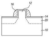
도 1a 및 도 1b는 종래의 스플리트 게이트 구조를 가지는 노어형 비휘발성 기억 소자의 구조를 나타내며, 도 1a는 복수개의 기억 셀이 배열된 셀 어레이의 상면도이고, 도 1b는 도 1a의 I-I 단면, 즉 워드 라인에 수직한 단면도이다. 도 1a 및 도 1b를 참조하면, 기판에 복수의 소자 분리막(20)이 형성되어 활성 영역(10)이 정의된다. 기판의 활성 영역(10) 위에는 복수개의 플로팅 게이트(16a)가 단위 셀마다 형성되고, 복수의 플로팅 게이트들(16a) 위에는 전극간 유전막(30)을 개재하여 제어 게이트(32)가 형성된다. 그리고, 단위 셀들은 공통 소스 라인(42)을 통해 병렬 접속된다. 여기서, 도면 부호 52는 상부에 형성된 금속 배선, 50은 콘택을 나타내며, 트랜지스터 소자들과 금속 배선은 층간 절연막에 의해 절연된다.1A and 1B show a structure of a NOR type nonvolatile memory device having a conventional split gate structure, FIG. 1A is a top view of a cell array in which a plurality of memory cells are arranged, and FIG. 1B is a cross-sectional view II of FIG. 1A, That is, the cross section perpendicular to the word line. 1A and 1B, a plurality of
도 1a 및 도 1b를 참조하면, 종래의 스플리트 게이트 구조를 가지는 노어형 비휘발성 기억 소자는, 전자를 가둘 수 있는 플로팅 게이트(16a)와 과잉 소거의 오동작을 방지하는 선택 트랜지스터용 선택 게이트(18)가 직렬로 연결되는 구조로 되어 있다. 이러한, 선택 트랜지스터의 추가로 인해 단위 셀의 사이즈가 커지게 되고, 선택 트랜지스터와 저장 트랜지스터의 각 채널을 각각의 게이트와 자기 정렬(Self-Aligned)시켜야 하는데, 소자의 제조 공정 능력을 감안한 마진 확보가 불가피하며 그로 인해 셀 사이즈가 증가하게 된다.1A and 1B, a conventional NOR type nonvolatile memory device having a split gate structure includes a
또한, 비휘발성 기억 소자는, 플로팅 게이트에 전자를 주입 및 제거함으로써 프로그램 및 소거 동작을 수행하기 때문에, 각각의 셀마다 플로팅 게이트를 독립적으로 형성해야 한다. 종래에는 하드 마스크를 사용하는 플로팅 게이트를 패터닝하고 있으나, 이 방법은 여러번의 식각 공정을 거쳐야 하므로 공정수가 증가한다. 또한, 보통 질화막을 하드 마스크로 사용하는데, 질화막을 식각하는 것 또한 공정의 부담으로 작용하게 된다. 아울러, 플로팅 게이트를 형성할 때 제어 게이트를 형성하기 위한 갭필 마진을 고려해야 하고, 또한 공통 소스 라인을 형성하기 위한 최소한의 마진도 고려해야 한다.In addition, since the nonvolatile memory device performs program and erase operations by injecting and removing electrons into the floating gate, the floating gate must be independently formed for each cell. Conventionally, a floating gate using a hard mask is patterned, but the number of processes increases because this method requires several etching processes. In addition, although a nitride film is usually used as a hard mask, etching the nitride film also acts as a burden on the process. In addition, when forming a floating gate, a gap fill margin for forming a control gate should be taken into consideration, and a minimum margin for forming a common source line should also be considered.
본 발명은 셀 면적이 현저히 감소된 스플리트 게이트 구조의 노어형 비휘발성 기억 소자를 제공하는 것을 목적으로 한다. 또한, 본 발명의 다른 목적은 하드 마스크를 사용하지 않고 플로팅 게이트를 형성할 수 있는 비휘발성 기억 소자의 제조 방법을 제공하는 것이다.An object of the present invention is to provide a NOR type nonvolatile memory device having a split gate structure with a significantly reduced cell area. Further, another object of the present invention is to provide a method of manufacturing a nonvolatile memory device capable of forming a floating gate without using a hard mask.
본 발명에 따른 스플리트 게이트를 가지는 노어형 비휘발성 기억 소자는, 반도체 기판 위로 돌출되어 형성된 블럭과, 상기 블럭의 일측벽에 형성된 제1 전극과, 상기 블럭 및 상기 제1 전극 위에 형성된 전극간 유전막과, 상기 전극간 유전막 위에 형성되고 상기 블럭의 상부로부터 상기 제1 전극의 측벽으로 연장되는 제2 전극으로 구성된 스플리트 게이트를 포함한다.A NOR-type nonvolatile memory device having a split gate according to the present invention includes a block protruding over a semiconductor substrate, a first electrode formed on one side wall of the block, an inter-electrode dielectric film formed on the block and the first electrode, And a split gate formed on the inter-electrode dielectric layer and formed of a second electrode extending from the top of the block to the sidewall of the first electrode.
여기서, 제1 전극은 상기 블럭의 측벽에 스페이서 형태로 형성된다. 또한, 블럭 및 제1 전극은 워드 라인 방향으로 복수개가 형성되어 셀 어레이를 구성한다. 아울러, 복수개의 블럭을 따라 형성된 공통 소스 라인이 형성된다.Here, the first electrode is formed in the form of a spacer on the side wall of the block. In addition, a plurality of blocks and first electrodes are formed in a word line direction to form a cell array. In addition, a common source line formed along the plurality of blocks is formed.
또한, 본 발명에 따른 스플리트 게이트를 가지는 노어형 비휘발성 기억 소자의 제조 방법은, (a) 반도체 기판 위에 워드 라인 방향으로 연장된 돌출부를 형성하는 단계와, (b) 상기 돌출부의 양 측벽에 워드 라인 방향으로 연장된 한쌍의 도전막 패턴을 형성하는 단계와, (c) 상기 돌출부 및 상기 한쌍의 도전막 패턴의 일부를 제거하여 워드 라인 방향으로 이격된 복수의 블럭 및 복수의 제1 전극쌍을 형성하는 단계와, (d) 상기 복수의 블럭 및 상기 복수의 제1 전극쌍 위에 전극간 유 전막 및 제2 전극을 순차적으로 형성하는 단계를 포함한다.In addition, the method for manufacturing a NOR-type nonvolatile memory device having a split gate according to the present invention includes the steps of: (a) forming a protrusion extending in a word line direction on a semiconductor substrate; and (b) a word on both sidewalls of the protrusion. Forming a pair of conductive film patterns extending in a line direction, and (c) removing the protrusions and a part of the pair of conductive film patterns to remove a plurality of blocks and a plurality of first electrode pairs spaced apart in a word line direction. And (d) sequentially forming an inter-electrode dielectric film and a second electrode on the plurality of blocks and the plurality of first electrode pairs.
기판에 돌출부를 형성한 후에, 상기 돌출부의 양측에 기판의 활성 영역을 정의하는 복수의 소자 분리막이 형성될 수 있다. 소자 분리막을 형성한 이후에는, 기판의 활성 영역 및 돌출부의 외벽에 터널 산화막을 형성한다. 또한, 한쌍의 제1 도전막 패턴은 상기 돌출부의 양 측벽에 스페이서 형태로 형성된다. 여기서, 공통 소스 라인은 복수의 블럭을 따라 연장되도록 형성된다.After the protrusions are formed on the substrate, a plurality of device isolation layers defining active regions of the substrate may be formed on both sides of the protrusions. After the device isolation film is formed, a tunnel oxide film is formed on the outer wall of the active region and the protrusion of the substrate. In addition, the pair of first conductive film patterns may be formed in a spacer form on both sidewalls of the protrusion. Here, the common source line is formed to extend along the plurality of blocks.
이하에서는 첨부한 도면을 참조하여 본 발명에 따른 스플리트 게이트 구조의 노어형 비휘발성 기억 소자 및 그 제조 방법의 바람직한 실시예를 설명하기로 한다.Hereinafter, a preferred embodiment of a NOR-type nonvolatile memory device having a split gate structure and a method of manufacturing the same according to the present invention will be described with reference to the accompanying drawings.
도 2a를 참조하면, 반도체 기판 예컨대 실리콘 기판(10)에 소정의 높이로 돌출된 돌출부(12)를 형성한다. 돌출부(12)는 기판(10)을 식각함으로써 형성될 수 있다. 돌출부(12)는 워드 라인 방향으로 연장되어 있다. 다음으로, 돌출부(12)의 양측으로 활성 영역을 정의하는 소자 분리막(20)이 복수개로 형성된다. 소자 분리막(20)은 활성 영역에 이웃하는 필드 영역에 형성된다(도 3 참조).Referring to FIG. 2A, a
한편, 소자 분리막(20)은 기판(10)에 돌출부(12)를 형성한 후에 형성되는 것이 바람직하고, 일반적인 소자 분리막 예컨대 STI(Shallow Trench Isolation) 공정을 통해 형성된다. 다만, 돌출부(12)로 인해 양측으로 분리되어 형성된다. STI를 형성할 때 트랜치 내부에 형성되는 STI 산화막은 습식 식각 공정을 통해 돌출부(12)가 형성되지 않은 기판(10)의 표면과 대략 일치하도록 제거된다.Meanwhile, the
다음으로 기판(10)의 활성 영역에 사진 공정 및 이온 주입 공정을 통해 셀의 문턱 전압을 조정한다. 그 후, 기판(10)의 전면에 폴리실리콘을 증착한 후 사진 공정 및 식각 공정을 통해 제1 도전막 패턴(16)을 형성한다. 이때, 제1 도전막 패턴(16)은 마스크 없이 에치백 공정을 통해 형성한다. 따라서, 제1 도전막 패턴(16)은 돌출부(12)의 측벽에 스페이서 형태로 형성된다. 제1 도전막 패턴(16)을 형성할 때 마스크를 사용하지 않으므로, 종래 사진 공정에서와 같이 고가의 노광 장비를 사용할 필요가 없다. 또한, 종래에는 고가의 노광 장비 대신에 하드 마스크를 이용하여 보다 미세한 선폭의 플로팅 게이트를 형성하는 방법이 이용되었으나, 본 발명에 따르면 하드 마스크도 사용할 필요가 없다. 또한, 스페이서 형태로 형성되는 플로팅 게이트는 식각 공정에서의 공정 변수를 제어함으로써 최소 선폭으로 형성될 수 있으며, 그에 따라 셀 면적이 현저히 감소하게 된다. 아울러, 돌출부(12)에 의해 이웃 셀과의 단락이 방지된다.Next, the threshold voltage of the cell is adjusted through a photo process and an ion implantation process in the active region of the
제1 도전막 패턴(16)을 형성하기 전에, 기판의 활성 영역을 산화시켜 산화막을 형성한다. 이때, 돌출부(12)의 외벽도 같이 산화되어 터널 산화막(14)이 형성된다.Before forming the first
다음으로, 돌출부(12) 및 스페이서 형태의 제1 도전막 패턴(16)을 비트 라인 식각 공정을 통해 패터닝한다. 도 3을 참조하면, 패터닝된 돌출부(12) 및 제1 도전막 패턴(16)은 각각 실리콘 블럭(12a) 및 제1 전극(16a)으로 분리된다. 따라서, 워드 라인 방향으로 복수의 실리콘 블럭(12a) 및 그 양 측벽에서 서로 대향하는 복수의 제1 전극쌍(16a)이 형성되어, 2개의 플로팅 게이트가 한 조를 이루면서 셀 어레이가 형성된다. 그 후, 도 3에서 보듯이, 기판의 활성 영역(10)에 도펀트를 이 온 주입하면, 복수의 실리콘 블럭(12a)을 따라 공통 소스 영역과 공통 소스 라인이 동시에 형성된다.Next, the
특히, 도 3에서 각각의 실리콘 블럭(12a)의 상면 및 전후 측벽에서 빗금으로 표시한 영역에 공통 소스(40s)가 형성되며, 비트 라인 식각 공정에 의해 일부가 제거되어 노출된 기판 영역 내에 소스 라인(42)이 형성된다. 그리고, 제1 전극(16a)의 좌측 또는 우측에 위치한 기판 영역에 주입된 도펀트에 의해 드레인 영역(40d)이 형된다.In particular, in FIG. 3, a
한편, 종래에는 공통 소스 라인(42)을 형성하기 위하여, 폴리실리콘, 실리콘 및 산화막의 식각 선택비를 이용하여 STI 산화막을 제거하는 SAS(Self-Aligned Source) 기술을 이용하였는데, 본 발명에 따르면 SAS 기술을 적용할 필요가 없다.Meanwhile, in order to form the
다음으로, 도 2c에서 보듯이, 기판 전면에 전극간 유전막(30)을 형성한다. 그리고, 전극간 유전막(30) 위에 폴리실리콘을 증착 및 패터닝하여 제어 게이트를 이루는 제2 전극(32)을 형성한다. 제2 전극(32)은 실리콘 블럭(12a) 및 제1 전극쌍(16a)을 완전히 덮도록 형성된다. 또한, 도 2c에서 보듯이, 실리콘 블럭(12a)의 상면에는 공통 소스 영역(40s)이 형성되어 있다. 실리콘 블럭(12a)의 전후 측벽에도 소스 영역이 형성되지만, 도 2c에는 편의상 나타내지 않았다.Next, as shown in FIG. 2C, an inter-electrode
본 발명에 따르면, 대칭 구조의 플로팅 게이트를 에치백 공정을 통해서 미세한 선폭으로 형성할 수 있다. 따라서, 고가의 노광 장비 또는 하드 마스크를 이용할 필요가 없으므로, 제조 공정이 상대적으로 단순하다. 또한 단위 셀의 면적이 최소화될 수 있으며, 아울러 공통 소스 라인을 형성하기 위하여 복잡한 SAS 공정을 거치지 않아도 된다. 그 결과, 소자의 제조 비용을 절감할 수 있으며, 제조 공정의 효율을 극대화할 수 있다.According to the present invention, a floating gate having a symmetrical structure can be formed with a fine line width through an etch back process. Thus, there is no need to use expensive exposure equipment or hard masks, so the manufacturing process is relatively simple. In addition, the area of the unit cell can be minimized, and a complicated SAS process is not required to form a common source line. As a result, the manufacturing cost of the device can be reduced, and the efficiency of the manufacturing process can be maximized.
지금까지 본 발명의 바람직한 실시예에 대해 설명하였으나, 본 발명이 속하는 기술분야에서 통상의 지식을 가진 자는 본 발명의 본질적인 특성을 벗어나지 않는 범위 내에서 변형된 형태로 구현할 수 있을 것이다. 그러므로 여기서 설명한 본 발명의 실시예는 한정적인 관점이 아니라 설명적인 관점에서 고려되어야 하고, 본 발명의 범위는 상술한 설명이 아니라 특허청구범위에 나타나 있으며, 그와 동등한 범위 내에 있는 모든 차이점은 본 발명에 포함되는 것으로 해석되어야 한다.Although a preferred embodiment of the present invention has been described so far, those skilled in the art will be able to implement in a modified form without departing from the essential characteristics of the present invention. Therefore, the embodiments of the present invention described herein are to be considered in descriptive sense only and not for purposes of limitation. Should be interpreted as being included in.
Claims (9)
Translated fromKoreanPriority Applications (2)
| Application Number | Priority Date | Filing Date | Title |
|---|---|---|---|
| KR1020050132722AKR100660284B1 (en) | 2005-12-28 | 2005-12-28 | Nonvolatile Memory Device with Split Gate Structure and Manufacturing Method Thereof |
| US11/646,092US20070147123A1 (en) | 2005-12-28 | 2006-12-26 | Split gate type non-volatile memory device and method of manufacturing the same |
Applications Claiming Priority (1)
| Application Number | Priority Date | Filing Date | Title |
|---|---|---|---|
| KR1020050132722AKR100660284B1 (en) | 2005-12-28 | 2005-12-28 | Nonvolatile Memory Device with Split Gate Structure and Manufacturing Method Thereof |
Publications (1)
| Publication Number | Publication Date |
|---|---|
| KR100660284B1true KR100660284B1 (en) | 2006-12-20 |
Family
ID=37815210
Family Applications (1)
| Application Number | Title | Priority Date | Filing Date |
|---|---|---|---|
| KR1020050132722AExpired - Fee RelatedKR100660284B1 (en) | 2005-12-28 | 2005-12-28 | Nonvolatile Memory Device with Split Gate Structure and Manufacturing Method Thereof |
Country Status (2)
| Country | Link |
|---|---|
| US (1) | US20070147123A1 (en) |
| KR (1) | KR100660284B1 (en) |
Families Citing this family (1)
| Publication number | Priority date | Publication date | Assignee | Title |
|---|---|---|---|---|
| US8320191B2 (en) | 2007-08-30 | 2012-11-27 | Infineon Technologies Ag | Memory cell arrangement, method for controlling a memory cell, memory array and electronic device |
Family Cites Families (2)
| Publication number | Priority date | Publication date | Assignee | Title |
|---|---|---|---|---|
| US6831325B2 (en)* | 2002-12-20 | 2004-12-14 | Atmel Corporation | Multi-level memory cell with lateral floating spacers |
| US7148538B2 (en)* | 2003-12-17 | 2006-12-12 | Micron Technology, Inc. | Vertical NAND flash memory array |
- 2005
- 2005-12-28KRKR1020050132722Apatent/KR100660284B1/ennot_activeExpired - Fee Related
- 2006
- 2006-12-26USUS11/646,092patent/US20070147123A1/ennot_activeAbandoned
Also Published As
| Publication number | Publication date |
|---|---|
| US20070147123A1 (en) | 2007-06-28 |
Similar Documents
| Publication | Publication Date | Title |
|---|---|---|
| US10741570B2 (en) | Nonvolatile memory devices having single-layered gates and methods of fabricating the same | |
| JP4109460B2 (en) | Nonvolatile semiconductor memory device and manufacturing method thereof | |
| US7553725B2 (en) | Nonvolatile memory devices and methods of fabricating the same | |
| KR20080010900A (en) | Nonvolatile Memory Device, Operation Method and Manufacturing Method Thereof | |
| KR100446308B1 (en) | Non-volatile memory device having select transistor structure and SONOS(Silicon-Oxide-Nitride-Oxide-Silicon) cell structure and method for fabricating the same | |
| CN108807400B (en) | P-channel flash memory cell, operating method and manufacturing method thereof, and flash memory device | |
| US20030127684A1 (en) | Split-gate type nonvolatile memory devices and methods for fabricating the same | |
| US11315635B2 (en) | Split-gate, 2-bit non-volatile memory cell with erase gate disposed over word line gate, and method of making same | |
| KR0155859B1 (en) | Flash memory device and manufacturing method thereof | |
| US6960527B2 (en) | Method for fabricating non-volatile memory device having sidewall gate structure and SONOS cell structure | |
| JP2006005357A (en) | Split gate flash memory device and manufacturing method thereof | |
| US7091090B2 (en) | Nonvolatile memory device and method of forming same | |
| US6998669B2 (en) | Memory cells with nonuniform floating gate structures | |
| KR100654559B1 (en) | NOR flash memory cell array and manufacturing method thereof | |
| US20100102375A1 (en) | Semiconductor device and manufacturing method thereof | |
| KR100606536B1 (en) | Nonvolatile Memory Device and Manufacturing Method Thereof | |
| KR100557531B1 (en) | Semiconductor device and manufacturing method thereof | |
| US8476694B2 (en) | Memory cell, memory device and method for manufacturing memory cell | |
| KR100660284B1 (en) | Nonvolatile Memory Device with Split Gate Structure and Manufacturing Method Thereof | |
| JP5030049B2 (en) | Flash memory device, driving method and manufacturing method thereof | |
| KR20090000444A (en) | Manufacturing method of nonvolatile memory device | |
| US7435649B2 (en) | Floating-gate non-volatile memory and method of fabricating the same | |
| KR100654359B1 (en) | Nonvolatile Memory Device Manufacturing Method | |
| KR100719738B1 (en) | Flash memory device and method of operating and manufacturing the same | |
| KR100642383B1 (en) | Flash memory device having improved erase efficiency and manufacturing method thereof |
Legal Events
| Date | Code | Title | Description |
|---|---|---|---|
| A201 | Request for examination | ||
| PA0109 | Patent application | St.27 status event code:A-0-1-A10-A12-nap-PA0109 | |
| PA0201 | Request for examination | St.27 status event code:A-1-2-D10-D11-exm-PA0201 | |
| PN2301 | Change of applicant | St.27 status event code:A-3-3-R10-R13-asn-PN2301 St.27 status event code:A-3-3-R10-R11-asn-PN2301 | |
| PN2301 | Change of applicant | St.27 status event code:A-3-3-R10-R13-asn-PN2301 St.27 status event code:A-3-3-R10-R11-asn-PN2301 | |
| E701 | Decision to grant or registration of patent right | ||
| PE0701 | Decision of registration | St.27 status event code:A-1-2-D10-D22-exm-PE0701 | |
| PR1002 | Payment of registration fee | St.27 status event code:A-2-2-U10-U11-oth-PR1002 Fee payment year number:1 | |
| GRNT | Written decision to grant | ||
| PR0701 | Registration of establishment | St.27 status event code:A-2-4-F10-F11-exm-PR0701 | |
| PG1601 | Publication of registration | St.27 status event code:A-4-4-Q10-Q13-nap-PG1601 | |
| PR1001 | Payment of annual fee | St.27 status event code:A-4-4-U10-U11-oth-PR1001 Fee payment year number:4 | |
| PR1001 | Payment of annual fee | St.27 status event code:A-4-4-U10-U11-oth-PR1001 Fee payment year number:5 | |
| FPAY | Annual fee payment | Payment date:20111121 Year of fee payment:6 | |
| PR1001 | Payment of annual fee | St.27 status event code:A-4-4-U10-U11-oth-PR1001 Fee payment year number:6 | |
| LAPS | Lapse due to unpaid annual fee | ||
| PC1903 | Unpaid annual fee | St.27 status event code:A-4-4-U10-U13-oth-PC1903 Not in force date:20121215 Payment event data comment text:Termination Category : DEFAULT_OF_REGISTRATION_FEE | |
| PC1903 | Unpaid annual fee | St.27 status event code:N-4-6-H10-H13-oth-PC1903 Ip right cessation event data comment text:Termination Category : DEFAULT_OF_REGISTRATION_FEE Not in force date:20121215 | |
| P22-X000 | Classification modified | St.27 status event code:A-4-4-P10-P22-nap-X000 | |
| P22-X000 | Classification modified | St.27 status event code:A-4-4-P10-P22-nap-X000 |