KR100659826B1 - Circuit board of battery pack - Google Patents
Circuit board of battery packDownload PDFInfo
- Publication number
- KR100659826B1 KR100659826B1KR1020050126138AKR20050126138AKR100659826B1KR 100659826 B1KR100659826 B1KR 100659826B1KR 1020050126138 AKR1020050126138 AKR 1020050126138AKR 20050126138 AKR20050126138 AKR 20050126138AKR 100659826 B1KR100659826 B1KR 100659826B1
- Authority
- KR
- South Korea
- Prior art keywords
- substrate
- circuit board
- battery pack
- bent
- substrates
- Prior art date
- Legal status (The legal status is an assumption and is not a legal conclusion. Google has not performed a legal analysis and makes no representation as to the accuracy of the status listed.)
- Active
Links
Images


Classifications
- H—ELECTRICITY
- H05—ELECTRIC TECHNIQUES NOT OTHERWISE PROVIDED FOR
- H05K—PRINTED CIRCUITS; CASINGS OR CONSTRUCTIONAL DETAILS OF ELECTRIC APPARATUS; MANUFACTURE OF ASSEMBLAGES OF ELECTRICAL COMPONENTS
- H05K3/00—Apparatus or processes for manufacturing printed circuits
- H05K3/36—Assembling printed circuits with other printed circuits
- H05K3/361—Assembling flexible printed circuits with other printed circuits
- H05K3/363—Assembling flexible printed circuits with other printed circuits by soldering
- H—ELECTRICITY
- H05—ELECTRIC TECHNIQUES NOT OTHERWISE PROVIDED FOR
- H05K—PRINTED CIRCUITS; CASINGS OR CONSTRUCTIONAL DETAILS OF ELECTRIC APPARATUS; MANUFACTURE OF ASSEMBLAGES OF ELECTRICAL COMPONENTS
- H05K1/00—Printed circuits
- H05K1/02—Details
- H05K1/14—Structural association of two or more printed circuits
- H—ELECTRICITY
- H01—ELECTRIC ELEMENTS
- H01R—ELECTRICALLY-CONDUCTIVE CONNECTIONS; STRUCTURAL ASSOCIATIONS OF A PLURALITY OF MUTUALLY-INSULATED ELECTRICAL CONNECTING ELEMENTS; COUPLING DEVICES; CURRENT COLLECTORS
- H01R12/00—Structural associations of a plurality of mutually-insulated electrical connecting elements, specially adapted for printed circuits, e.g. printed circuit boards [PCB], flat or ribbon cables, or like generally planar structures, e.g. terminal strips, terminal blocks; Coupling devices specially adapted for printed circuits, flat or ribbon cables, or like generally planar structures; Terminals specially adapted for contact with, or insertion into, printed circuits, flat or ribbon cables, or like generally planar structures
- H01R12/50—Fixed connections
- H01R12/51—Fixed connections for rigid printed circuits or like structures
- H01R12/52—Fixed connections for rigid printed circuits or like structures connecting to other rigid printed circuits or like structures
- H—ELECTRICITY
- H05—ELECTRIC TECHNIQUES NOT OTHERWISE PROVIDED FOR
- H05K—PRINTED CIRCUITS; CASINGS OR CONSTRUCTIONAL DETAILS OF ELECTRIC APPARATUS; MANUFACTURE OF ASSEMBLAGES OF ELECTRICAL COMPONENTS
- H05K1/00—Printed circuits
- H05K1/02—Details
- H05K1/14—Structural association of two or more printed circuits
- H05K1/148—Arrangements of two or more hingeably connected rigid printed circuit boards, i.e. connected by flexible means
- H—ELECTRICITY
- H05—ELECTRIC TECHNIQUES NOT OTHERWISE PROVIDED FOR
- H05K—PRINTED CIRCUITS; CASINGS OR CONSTRUCTIONAL DETAILS OF ELECTRIC APPARATUS; MANUFACTURE OF ASSEMBLAGES OF ELECTRICAL COMPONENTS
- H05K2201/00—Indexing scheme relating to printed circuits covered by H05K1/00
- H05K2201/20—Details of printed circuits not provided for in H05K2201/01 - H05K2201/10
- H05K2201/2009—Reinforced areas, e.g. for a specific part of a flexible printed circuit
- H—ELECTRICITY
- H05—ELECTRIC TECHNIQUES NOT OTHERWISE PROVIDED FOR
- H05K—PRINTED CIRCUITS; CASINGS OR CONSTRUCTIONAL DETAILS OF ELECTRIC APPARATUS; MANUFACTURE OF ASSEMBLAGES OF ELECTRICAL COMPONENTS
- H05K2203/00—Indexing scheme relating to apparatus or processes for manufacturing printed circuits covered by H05K3/00
- H05K2203/01—Tools for processing; Objects used during processing
- H05K2203/0191—Using tape or non-metallic foil in a process, e.g. during filling of a hole with conductive paste
- H—ELECTRICITY
- H05—ELECTRIC TECHNIQUES NOT OTHERWISE PROVIDED FOR
- H05K—PRINTED CIRCUITS; CASINGS OR CONSTRUCTIONAL DETAILS OF ELECTRIC APPARATUS; MANUFACTURE OF ASSEMBLAGES OF ELECTRICAL COMPONENTS
- H05K3/00—Apparatus or processes for manufacturing printed circuits
- H05K3/0058—Laminating printed circuit boards onto other substrates, e.g. metallic substrates
Landscapes
- Engineering & Computer Science (AREA)
- Microelectronics & Electronic Packaging (AREA)
- Manufacturing & Machinery (AREA)
- Battery Mounting, Suspending (AREA)
- Combinations Of Printed Boards (AREA)
Abstract
Translated fromKoreanDescription
Translated fromKorean도 1은 종래의 배터리 팩의 회로 기판을 나타내는 대략적인 평면도이다.1 is a schematic plan view showing a circuit board of a conventional battery pack.
도 2는 도 1의 회로 기판을 절곡 시켰을 때의 상태를 나타내는 대략적인 단면도이다.FIG. 2 is a schematic cross-sectional view showing a state when the circuit board of FIG. 1 is bent.
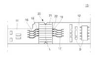
도 3은 본 발명의 일 실시예에 따른 배터리 팩의 회로 기판을 나타내는 대략 평면도이다. 3 is a schematic plan view showing a circuit board of a battery pack according to an embodiment of the present invention.
도 4는 도 3의 연성 인쇄 회로 기판(FPCB)의 구성을 나타내는 단면도이다.4 is a cross-sectional view illustrating a configuration of the flexible printed circuit board FPCB of FIG. 3.
도 5는 도 3의 회로 기판을 절곡 시켰을 때의 상태를 나타내는 대략적인 단면도이다.5 is a schematic cross-sectional view showing a state when the circuit board of FIG. 3 is bent.
< 도면의 주요 부호에 대한 간단한 설명 ><Brief Description of Major Codes in Drawings>
10, 100: 회로 기판11, 111: 제 1 기판(PCB)10, 100:
12, 112: 제 2 기판(PCB)16,17,116,117: 배선 패턴12, 112: second substrate (PCB) 16, 17, 116, 117: wiring pattern
18,19,118,119: 단자부20, 120: 제 3 기판(FPCB)18, 19, 118, 119:
21, 121: 패드12,122: 솔더링된 솔더21, 121: pad 12,122: soldered solder
125: 절연층126: 솔더층125: insulating layer 126: solder layer
130: 보호용 테이프130: protective tape
본 발명은 배터리 팩에 관한 것으로, 보다 상세하게는 저가의 연성 인쇄 회로 기판에 테이프를 부착함으로써 절곡시 발생하는 크랙(crack)을 방지할 수 있는 배터리 팩의 회로 기판에 관한 것이다.BACKGROUND OF THE INVENTION 1. Field of the Invention The present invention relates to a battery pack, and more particularly, to a circuit board of a battery pack capable of preventing cracks generated during bending by attaching a tape to a low cost flexible printed circuit board.
일반적으로 노트북 컴퓨터 등의 휴대형 전자기기는 기기의 동작 전원으로 외부에서 공급하는 110/220V 의 상용 교류전원을 이용하는 것 외에, 상술한 교류 전원 공급 없이 일정시간 동안 전자기기를 사용할 수 있도록 하는 배터리 팩을 이용한다. 즉, 휴대형 전자기기에 형성된 수납 공간에 배터리 팩을 전기적 및 기계적으로 연결하여, 배터리 팩에 충전된 전원을 휴대형 전자기기의 동작 전원으로 사용함으로써, 전원이 공급되지 않는 곳에서 편리하게 사용할 수 있도록 하고 있다.In general, a portable electronic device such as a notebook computer uses a 110 / 220V commercial AC power supplied from the outside as the operating power of the device, and a battery pack that allows the electronic device to be used for a predetermined time without the aforementioned AC power supply. I use it. That is, by connecting the battery pack electrically and mechanically to the storage space formed in the portable electronic device, by using the power charged in the battery pack as the operating power of the portable electronic device, it can be conveniently used in the place where the power is not supplied have.
한편, 이러한 배터리 팩은 복수의 베어 셀과, 상기 베어 셀의 충방전 등을 제어하는 보호 회로가 형성된 보호 회로 기판과, 상기 베어 셀과 상기 보호 회로를 전기적으로 연결해주는 단자선을 포함하여 이루어진다. 이 베어 셀들과, 보호 회로 기판과 단자선은 소정 케이스에 수납된 채 사용될 수도 있다.The battery pack includes a plurality of bare cells, a protection circuit board on which a protection circuit for controlling charge and discharge of the bare cells is formed, and a terminal line electrically connecting the bare cell and the protection circuit. These bare cells, the protective circuit board, and the terminal line may be used in a predetermined case.
상기와 같은 배터리 팩은 다수의 베어 셀을 소정의 전압과 전류를 갖도록 직렬 또는 병렬로 탭부재를 사용하여 연결하고, 직병렬로 연결된 베어 셀들 중 한 셀의 단자에 연결된 단자선, 예를 들어 도전성 탭 또는 배선(wire)을 충방전과 다수 의 베어 셀의 작동을 제어하는 보호회로를 갖는 보호 회로 기판에 연결하고 납땜을 실시하여 베어 셀과 보호 회로 기판을 전기적으로 연결한다.The battery pack is connected to a plurality of bare cells using a tab member in series or in parallel to have a predetermined voltage and current, and a terminal line connected to a terminal of one of the bare cells connected in parallel, for example, conductive The tab or wire is connected to a protective circuit board having a protection circuit that controls charging and discharging and operation of a plurality of bare cells, and soldered to electrically connect the bare cell and the protection circuit board.
이렇게 베어 셀과 전기적으로 연결되는 보호 회로와, 외부의 전자기기와 연결되는 커넥터는 보호회로 기판을 통과하는 도전구조에 의해 전기 접속되어 있다. 또한, 보호 회로 기판에는 서미스터(thermistor), 열퓨즈(thermer fuse), 양성온도계수(positive temperature coefficient) 소자와 같은 보호소자 등도 연결될 수 있다.The protective circuit electrically connected to the bare cell and the connector connected to the external electronic device are electrically connected by a conductive structure passing through the protective circuit board. In addition, a protection device such as a thermistor, a thermal fuse, or a positive temperature coefficient device may be connected to the protection circuit board.
상기와 같이, 일반적인 배터리 팩은 케이스 내에 복수개의 베어 셀 전지를 내장한다. 케이스 내에는 보호 회로 등의 회로 패턴상에 커넥터와 전자부품을 실장한 회로 기판이 부착된다. 회로 기판은 베어 셀 전지와 외부와의 사이에 전기신호를 주고 받기 위한 것이다. 전자제품이 소형화되고 복잡해 지고 있는 추세에 있어서, 케이스의 크기가 작아진 배터리 팩에 회로 기판을 부착하기 위해서는 케이스의 내부공간을 효율적으로 쓰는 것이 필요하다. 이를 위한 한가지 방법으로 회로 기판을 절곡 시켜 내장하는 것이 있다.As described above, a general battery pack includes a plurality of bare cell batteries in a case. In the case, a circuit board having a connector and an electronic component mounted thereon is attached on a circuit pattern such as a protective circuit. The circuit board is for transmitting and receiving electrical signals between the bare cell battery and the outside. In the trend of miniaturization and complexity of electronic products, it is necessary to efficiently use the internal space of the case in order to attach a circuit board to a battery pack having a smaller case size. One way to do this is to bend and embed the circuit board.
도 1은 종래의 배터리 팩의 회로 기판을 나타내는 대략적인 평면도이다.1 is a schematic plan view showing a circuit board of a conventional battery pack.
도 1에 도시된 바와 같이, 종래의 배터리 팩의 회로 기판(10)은 소정의 회로 패턴이 형성된 제 1 기판(11), 소정의 회로 패턴이 형성된 제 2 기판(12) 및 제 1 기판(11)과 제 2 기판(12)을 전기적으로 연결하는 제 3 기판(20)을 구비하여 이루어진다.As shown in FIG. 1, a
회로 기판(10)의 제 1 및 제 2 기판(11,12)은 절곡선 L을 사이에 두고 서로 물리적으로 연결되어있다. 그리고, 제 1 기판(11)의 일측과 제 3 기판의 일측이 연결되고 제 2 기판(12)의 일측과 제 3 기판(20)의 타측이 연결된 상태에서, 제 1 기판(11)과 제 2 기판(12)는 서로 도통 접속된다. 상기와 같은 제 3 기판(20)은 연성 인쇄 회로 기판(Flexible printed circuit board)으로서 회로 패턴을 구성하며 구부림이 가능하다. 이에 따라, 회로 기판(10)을 케이스의 한정된 공간에 부착시키기 위해 제 1 기판(11)과 제 2 기판(12)이 절곡선 L을 통해 소정각도로 절곡되어 물리적으로 분리되었을 때, 제 3 기판(20)은 제 1 기판(11)과 제 2 기판(12)을 전기적으로 연결시켜주는 역할을 한다.The first and
회로 기판(10)의 구성을 더 자세히 살펴보면, 제 1 및 제 2 기판(11,12)의 각각의 일면 또는 양면에는 소정의 패턴이 형성되어 있으며, 제 1 기판(11)과 제 2 기판(12)의 표면에는 커넥터(미도시) 또는 반도체 칩이나 저항기 등의 전자부품 D가 실장 되어 있다. 전자 부품 D는 배선패턴(16,17)과 전기적으로 도통 접속되어 있다. 그리고, 제 1 기판(11)의 일측과 제 3 기판(20)의 일측이 연결될 부분에는 배선 패턴(16)과 연결된 단자부(18)가 형성되어 있으며, 제 2 기판(12)의 일측과 제 3 기판(20)의 타측이 연결된 부분에는 배선 패턴(17)과 연결된 단자부(19)가 형성되어 있다. 단자부(18, 19)는 솔더링을 통해서 제 3 기판(20)의 회로패턴(21,이하 패드라 한다)과 전기적으로 연결된다. 여기서, 도면 부호 22는 솔더링된 솔더를 나타낸다. 이렇게 제 3 기판(20)의 패드(21)를 통해서 연결된 제 1 및 제 2 기판(11,12)은 전기적으로 일체가 되어 하나의 기판으로서의 기능을 한다. 이러한 회로 기판(10)이 케이스(미도시)내에 전지 이외에 한정된 공간에 배치되기 위해, 회로 기판(10)의 제 1 기판(11)과 제 2 기판(12)이 절곡선 L을 따라 절곡 분리된다. 이렇게 제 1 기판(11)과 제 2 기판(12)이 물리적으로 분리되더라도 제 3 기판을 통해 서로 도통이 되어, 배터리 전력 또는 전기신호가 회로기판(10)의 커넥터나 전자부품을 통해 전지(미도시)와 외부 기기사이에서 교환된다.Looking at the configuration of the
도 2는 도 1의 회로 기판을 절곡 시켰을 때의 상태를 나타내는 대략적인 단면도이다.FIG. 2 is a schematic cross-sectional view showing a state when the circuit board of FIG. 1 is bent.
제 1 기판(11)의 일측과 제 3 기판(20)의 일측, 제 2 기판(12)의 일측과 제 3 기판(20)의 타측을 접합하기 위해서는, 종래에는 핫바(hot bar)방식을 사용했다. 이 방식은 우선, 제 1 기판(11)의 일측과 제 3 기판(20)의 일측이 연결될 영역과, 제 2 기판(12)과 제 3 기판(20)의 타측이 연결될 영역에 SnPb와 같은 솔더(solder)를 인쇄한다. 그리고, 솔더가 인쇄된 제 3 기판(20)을 핫바(hot bar)로 눌러 솔더링을 실시한다. 이에 따라, 솔더링된 솔더(22)를 통해 제 1 기판(11)의 일측과 제 3 기판(20)의 일측 및 제 2 기판(12)과 제 3 기판(20)의 타측이 접합된다.In order to join one side of the
이러한 방식으로 접합된 회로 기판(10)을 도 1의 절곡선 L을 따라 절곡하면, 솔더링된 솔더(22) 부분의 제 3 기판(20)에 크랙(crack)이 발생될 수 있다. 다시 말하면, 핫바로 솔더를 솔더링 할 경우 솔더링된 솔더(22)의 두께가 일정하지 않아, 기판이 절곡될 때와 같은 외부 영향이 있을 경우에 솔더링된 솔더(22), 특히 핫바로 눌러 녹였을때 일정하게 눌려지지 않아 조금 튀어나온 부분이 회로 기판(10)의 절곡시 발생되는 힘에 영향을 받아 유연한 재질의 제 3 기판에 크랙(crack)을 발생시킬 수 있다. 이렇게 제 3 기판(20)에 발생한 크랙(crack)은 회로 기판 (10)의 절곡에 의해 물리적으로 분리되는 제 1 기판(11)과 제 2 기판(12)의 전기적 연결을 끊을 수 있다. 이로 인해 전지와 외부 기기와의 전기 신호를 교환할 수 없게 되는 문제점이 발생한다.When the
상기와 같은 문제점으로, 저가의 FPCB 대신에 flame leader 부품을 이용한 flame lead 방식으로 회로 기판을 제조하여 전지의 케이스에 내장하기도 한다. 이러한 flame lead 방식을 이용해 제조된 회로 기판은 절곡시 크랙(crack) 발생률이 적지만, flame leader 부품이 고가일 뿐 아니라 고가의 flame leader 부품을 이용한 flame lead 방식에서 거치는 리플로우(reflow) 공정을 위한 공정장비 또한 고가이므로 flame lead 방식은 비용면에서 비효율적이다.Due to the above problems, a circuit board may be manufactured in a flame lead method using a flame leader component instead of a low-cost FPCB and embedded in a battery case. The circuit board manufactured by using the flame lead method has a low cracking rate when bending, but the flame leader parts are not only expensive but also used for the reflow process through the flame lead method using the expensive flame leader parts. As the process equipment is also expensive, the flame lead method is inefficient in terms of cost.
따라서, 저가의 FPCB를 사용하면서 회로 기판을 절곡할때 크랙(crack) 불량을 방지할 수 있는 구조가 요구되고 있다.Therefore, there is a demand for a structure that can prevent crack defects when bending a circuit board while using a low cost FPCB.
본 발명은 상술한 종래의 문제점을 해결하기 위한 것으로, 저가의 연성 인쇄 회로 기판에 테이프를 부착함으로써 절곡시 크랙(crack)을 방지할 수 있는 배터리 팩의 회로 기판을 제공하는 것을 목적으로 한다.SUMMARY OF THE INVENTION The present invention has been made to solve the above-described problems, and an object of the present invention is to provide a circuit board of a battery pack capable of preventing cracks during bending by attaching a tape to a low cost flexible printed circuit board.
상기 목적을 달성하기 위한 본 발명의 실시예에 따른 배터리 팩의 회로 기판은 소정의 배선패턴이 형성된 제 1 기판과; 상기 제 1 기판과 절곡라인을 통해 절곡되어 물리적으로 분리되며 소정의 배선 배턴이 형성된 제 2 기판; 및 일측이 상기 제 1 기판의 일측과, 타측이 상기 제 2 판의 일측과 연결되어 상기 제 1 및 제 2 기판의 절곡라인에 걸쳐 형성되어 상기 제 1 및 제 2 기판의 배선패턴을 전기적으로 연결시키는 구부림 가능한 제 3 기판을 포함하며, 상기 제 1 기판과 상기 제 3 기판이 겹치는 제 1 영역과, 상기 제 2 기판과 상기 제 3 기판이 겹치는 제 2 영역에 보호용 테이프가 형성됨을 특징으로 한다.The circuit board of the battery pack according to an embodiment of the present invention for achieving the above object comprises a first substrate with a predetermined wiring pattern; A second substrate that is bent through the first substrate and the bending line to be physically separated and has a predetermined wiring baton; And one side connected to one side of the first substrate and the other side to one side of the second plate to be formed over the bent lines of the first and second substrates to electrically connect the wiring patterns of the first and second substrates. And a bendable third substrate, wherein the protective tape is formed in a first region where the first substrate and the third substrate overlap and a second region where the second substrate and the third substrate overlap.
상기 보호용 테이프는 상기 절곡라인과 평행하게 상기 제 1 영역과 제 2 영역의 각각의 외부면을 둘러가며 부착되며, 상기 보호용 테이프의 폭은 상기 절곡라인으로부터 상기 제 1 및 제 2 기판 각각과 상기 제 3 기판이 연결되는 부분까지의 거리로 이루어질 수 있다.The protective tape is attached to the outer surface of each of the first area and the second area in parallel with the bending line, and the width of the protective tape extends from each of the first and second substrates from the bending line. 3 may be a distance to the portion where the substrate is connected.
상기 보호용 테이프는 난연성 재질로 이루어질 수 있으며, 상기 보호용 테이프의 기재는 폴리에스테르(Polyester) 재질로 이루어질 수 있다.The protective tape may be made of a flame retardant material, and the substrate of the protective tape may be made of a polyester material.
이하 도면을 참조하면서 실시예를 통해 본 발명을 보다 상세히 설명하기로 한다.Hereinafter, the present invention will be described in more detail with reference to the accompanying drawings.
일반적인 배터리 팩은 케이스 내에 복수개의 베어 셀 전지를 내장한다. 케이스 내에는 보호 회로 등의 회로 패턴상에 커넥터와 전자부품을 실장한 회로 기판이 부착된다. 회로 기판은 베어 셀 전지와 외부와의 사이에 전기신호를 주고 받기 위한 것이다.A typical battery pack includes a plurality of bare cell batteries in a case. In the case, a circuit board having a connector and an electronic component mounted thereon is attached on a circuit pattern such as a protective circuit. The circuit board is for transmitting and receiving electrical signals between the bare cell battery and the outside.
도 3은 본 발명의 일 실시예에 따른 배터리 팩의 회로 기판을 나타내는 대략 평면도이며, 도 4는 도 3의 연성 인쇄 회로 기판(FPCB)의 구성을 나타내는 단면도이다.3 is a schematic plan view illustrating a circuit board of a battery pack according to an exemplary embodiment of the present invention, and FIG. 4 is a cross-sectional view illustrating a configuration of the flexible printed circuit board FPCB of FIG. 3.
도 3에 도시된 바와 같이, 본 발명의 일 실시예에 따른 배터리 팩의 회로 기 판(110)은 소정의 회로 패턴이 형성된 제 1 기판(111); 소정의 회로 패턴이 형성된 제 2 기판(112); 및 제 1 기판(111)과 제 2 기판(112)을 전기적으로 연결하는 제 3 기판(120)을 구비하여 이루어진다. 또한, 제 1 기판(111)과 제 3 기판(120)이 연결되는 영역과, 제 2 기판(112)과 제 3 기판(120)이 연결되는 영역에 부착되는 보호용 테이프(130)가 더 구비된다.As shown in FIG. 3, a
회로 기판(110)의 제 1 및 제 2 기판(111,112)은 절곡선 L을 사이에 두고 서로 물리적으로 연결되어있다. 그리고, 제 1 기판(111)의 일측과 제 3 기판(120)의 일측이 연결되고 제 2 기판(112)의 일측과 제 3 기판(120)의 타측이 연결된 상태에서, 제 1 기판(111)과 제 2 기판(112)는 서로 도통 접속된다. 상기와 같은 제 3 기판(120)은 연성 인쇄 회로 기판(Flexible printed circuit board)으로서 회로 패턴을 구성하며 구부림이 가능하다. 이에 따라, 회로 기판(110)을 케이스의 한정된 공간에 부착시키기 위해 제 1 기판(111)과 제 2 기판(112)이 절곡선 L을 통해 소정각도로 절곡되어 물리적으로 분리되었을 경우, 제 3 기판(120)은 제 1 기판(111)과 제 2 기판(112)을 전기적으로 연결해주는 역할을 한다.The first and
회로 기판(110)의 구성을 자세히 살펴보면, 제 1 및 제 2 기판(111,112)의 각각의 일면 또는 양면에는 소정의 패턴이 형성되어 있으며, 제 1 기판(111)과 제 2 기판(112)의 표면에는 커넥터(미도시) 또는 반도체 칩이나 저항기 등의 전자부품 D가 실장 되어 있다.전자 부품 D는 배선패턴(116,117)과 전기적으로 도통 접속되어 있다. 그리고, 제 1 기판(11)의 일측과 제 3 기판(120)의 일측이 연결될 부분에는 배선 패턴(116)과 연결된 단자부(118)가 형성되어 있으며, 제 2 기판(112)의 일측 과 제 3 기판(120)의 타측이 연결된 부분에는 배선 패턴(117)과 연결된 단자부(119)가 형성되어 있다. 단자부(118, 119)는 솔더링을 통해서 제 3 기판(120)의 회로패턴(121,이하 패드라 한다)과 전기적으로 연결된다. 여기서, 도면 부호 122는 솔더링된 솔더를 나타낸다. 이렇게 제 3 기판(120)의 패드(121)를 통해서 연결된 제 1 및 제 2 기판(111,112)은 전기적으로 일체가 되어 하나의 기판으로서의 기능을 한다. 이러한 회로 기판(110)이 케이스(미도시)내에 전지 이외에 한정된 공간에 배치되기 위해, 회로 기판(110)의 제 1 기판(111)과 제 2 기판(112)이 절곡선 L을 따라 절곡 분리된다. 이렇게 제 1 기판(111)과 제 2 기판(112)이 물리적으로 분리되더라도 제 3 기판(120)을 통해 서로 도통이 되어, 배터리 전력 또는 전기신호가 회로기판(110)의 커넥터나 전자부품을 통해 전지(미도시)와 외부 기기사이에서 교환된다.Looking at the configuration of the
상기와 같은 제 1 기판(111)과 제 2 기판(112)은 PCB(printed circuit board)로서 페놀수지(phenol Resin) 또는 에폭시 수지로 된 평판 위에 회로 패턴이 형성되어 이루어진다.The
그리고, 제 1 기판(111)과 제 2 기판(112)를 전기적으로 연결시키는 구부림이 가능한 제 3 기판(FPCB; 120)은 기판 필름(base film)으로서, 도 4에 도시된 바와 같이, 얇은 절연 필름(125) 위에 동박(Cu;121)으로 회로(이하, 패드라 한다)를 구성하도록 하고 Cu 패드(121)위에 다시 절연 필름(125)을 코팅하여 구성된다. 이때, 제 3 기판(120)은 제 1 기판(111) 및 제 2 기판(112)과 접착하기 위해 양 단부의 접착되는 부위에 SnPb와 같은 솔더층(126)을 형성한다.In addition, the bendable
제 1 기판(111)의 일측과 제 3 기판(120)의 일측, 제 2 기판(112)의 일측과 제 3 기판(20)의 타측을 접합하기 위해서는, 우선, 제 1 기판(111)의 일측과 제 3 기판(120)의 일측이 연결될 영역 및 제 2 기판(112)과 제 3 기판(120)의 타측이 연결될 영역에 SnPb와 같은 솔더(solder)를 인쇄한다. 그리고, 솔더가 인쇄된 부분의 제 3 기판(120)을 핫바(hot bar)로 눌러 솔더링을 실시한다. 이에 따라, 솔더링된 솔더(122)를 통해 제 1 기판(111)의 일측과 제 3 기판(120)의 일측 및 제 2 기판(112)과 제 3 기판(120)의 타측이 접합된다. 따라서, 제 1 기판(111)과 제 2 기판(112)이 제 3 기판(120)을 통해 전기적으로 연결된다.To join one side of the
그리고, 절곡선 L 부분을 제외하고 제 1 기판(111)과 제 3 기판(120)이 겹치는 영역 A와 제 2 기판(112)과 제 3 기판(120)이 겹치는 영역 B에 본 발명의 특징인 보호용 테이프(130)를 부착시킨다. 이때, 보호용 테이프(130)는 A와 B영역 각각의 양면을 모두 감싸도록 절곡선 L과 평행하게 절곡선 L을 따라 둘러가며 부착된다.Except for the bent line L portion, the region A where the
도 5는 도 3의 회로 기판을 절곡 시켰을 때의 상태를 나타내는 대략적인 단면도이다.5 is a schematic cross-sectional view showing a state when the circuit board of FIG. 3 is bent.
본 발명의 일 실시예에 따라, 제 1 기판(111)과 제 3 기판(120)이 겹치는 영역 A와 제 2 기판(112)과 제 3 기판(120)이 겹치는 영역 B 각각의 양면에 보호용 테이프(130)가 부착된 회로 기판(110)은 케이스 내의 공간을 효율적으로 사용하기 위해 절곡이 이루어진다.According to one embodiment of the invention, the protective tape on both sides of each of the region A where the
제 1 기판(111)의 일측과 제 3 기판(120)의 일측, 및 제 2 기판(112)의 일측 과 제 3 기판(120)의 타측이 핫바(hot bar) 방식으로 접합되어, 제 1 및 제 2 기판(111,112) 각각과 제 3 기판(120)이 겹치는 영역(A,B)이 생긴다. 이 영역(A,B)에 본 발명의 특징인 보호용 테이프(130)가 부착되면, 제 1 기판 및 제 2 기판(111,112) 각각과 제 3 기판(120)이 솔더링된 솔더(122) 부분이 보호용 테이프(130)로 고정되어, 회로 기판(110)의 절곡시 발생되는 힘의 영향이 적어진다. 이에 따라, 제 3 회로 기판의 솔더링된 솔더(112) 부분에서 발생하는 크랙(crack)이 방지될 수 있다. 이러한 보호용 테이프(130)는 회로 기판에서 발생될수 있는 열에 대해 강하도록 난연성 재질로 형성될 수 있다. 이에 따라, 보호용 테이프(130)의 기재는 폴리에스테르 (Polyester) 재질로 형성될 수 있다. 보호용 테이프(130)의 폭은 도 3의 절곡선 L로부터 제 1 및 제 2 기판(111,112) 각각의 솔더링된 솔더(122) 부분까지 커버할 수 있는 거리로 이루어질 수 있다.One side of the
상기와 같이, 제 1 및 제 2 기판(111,112) 각각의 일측에 제3 기판(20)을 연결시켜 제 1 기판(111)과 제 3 기판(120)이 겹치는 부분과 제 2 기판(112)과 제 3 기판(120)이 겹치는 부분을 보호 테이프(130)로 부착한 후 제 1 기판(111)과 제 2 기판(112)을 절곡 분리할 경우, 제 1 기판(111)과 제 3 기판(120)이 겹치는 부분과 제 2기판(112)과 제 3 기판(120)이 겹치는 부분이 보호용 테이프(130)에 의해 부분이 들뜨지 않고 고정이 된다. 이에 따라, 제 1 기판(111)의 일측과 제 3 기판(120)의 타측 사이, 및 제 2 기판(112)의 일측과 제 3 기판(120)의 타측 사이 각각에 형성된 솔더링된 솔더(122)는 회로 기판(110)의 절곡시 발생하는 힘과 같은 외력에 의한 충격을 덜 받게 된다. 따라서, 본 발명의 실시예에 따라 보호용 테이프가 구 비된 회로 기판은 종래의 보호 부재 없이 절곡될 때 회로 기판에서 발생했던 크랙(crack)을 방지할 수 있다.As described above, the
다음은 종래의 보호 부재를 구비하지 않은 회로 기판과 본 발명의 실시예에 따라 보호용 테이프가 구비된 회로 각각을 회로 기판의 모듈별로 절곡 시켜 크랙발생 여부를 테스트한 결과이다. 표 1은 종래의 보호부재를 구비하지 않은 회로 기판의 크랙 발생 여부를 테스트한 결과를 나타낸 것이며, 표 2는 본 발명의 실시예에 따라 보호용 테이프를 구비한 회로 기판의 크랙 발생 여부를 테스트한 결과이다.The following is a test result of crack generation by bending each of the circuit boards without the protection member and the circuit with the protection tape according to the embodiment of the present invention for each module of the circuit board. Table 1 shows the results of testing whether the crack of the circuit board is not provided with a conventional protection member, Table 2 shows the results of testing the crack of the circuit board having a protective tape according to an embodiment of the present invention to be.


표 1 및 표 2에서 'OK'는 크랙이 발생하지 않은 것을 나타내며, 'NG'는 크랙이 발생한 것을 나타낸다. 표 1의 테스트 결과를 살펴보면, 보호부재를 구비하지 않은 회로 기판중 몇개는 절곡됐을때 크랙이 발생되었다. 그런데 표 2의 결과를 살펴보면, 보호용 테이프를 구비한 회로 기판 모두는 크랙이 발생되지 않았다. 따라서, 상기와 같은 테스트 결과를 통해, 보호용 테이프를 회로 기판에 부착하면 회로 기판의 크랙이 방지될 수 있다는 것을 알 수 있다.In Table 1 and Table 2, 'OK' indicates that no crack occurred, and 'NG' indicates that cracks occurred. In the test results of Table 1, some of the circuit boards without the protection member were cracked when they were bent. By the way, look at the results of Table 2, all of the circuit board with a protective tape did not cause cracks. Therefore, through the above test results, it can be seen that the crack of the circuit board can be prevented by attaching the protective tape to the circuit board.
상술한 바와 같이, 본 발명의 실시예에 따른 배터리 팩의 회로 기판은 연성 인쇄 회로 기판(FPCB)과 경성 인쇄 회로 기판(PCB)이 겹치는 영역의 양면에 보호용 테이프를 둘러가며 부착하여 FPCB와 PCB가 겹치는 영역을 고정함으로써, 솔더링 된 솔더가 형성된 부분의 FPCB가 회로 기판(110)의 절곡시 발생하는 힘과 같은 외력에 의한 충격으로부터 보호되어 FPCB의 크랙(crack)을 방지할 수 있다. 이에 따라, 전지와 외부 기기의 전기적인 연결이 끊어지는 것을 방지할 수 있어 전지와 외부 기기와의 전기 신호를 교환할 수 있다.As described above, the circuit board of the battery pack according to the embodiment of the present invention is attached to the both sides of the protective tape on both sides of the overlapping area of the flexible printed circuit board (FPCB) and the rigid printed circuit board (PCB) by attaching the FPCB and PCB By fixing the overlapping regions, the FPCB of the soldered solder-formed portion may be protected from an external force such as a force generated when the
또한, 본 발명의 실시예에 따른 배터리 팩의 회로 기판은 저가의 FPCB를 이용하여 핫바(hot bar) 방식으로 형성되어 고가의 flame leader 부품을 이용하여 flame lead 방식으로 형성되는 회로 기판보다 제조면에서 비용을 크게 줄일 수 있어 제조 수율을 증가시킬 수 있다.In addition, the circuit board of the battery pack according to the embodiment of the present invention is formed in a hot bar (hot bar) method using a low-cost FPCB in terms of manufacturing than a circuit board formed by a flame lead method using expensive flame leader components The cost can be greatly reduced, leading to increased manufacturing yields.
이상 설명한 바와 같이, 본 발명은 상술한 특정의 바람직한 실시예에 한정되지 아니하며, 특허청구범위에서 청구하는 본 발명의 요지를 벗어남이 없이 당해 발명이 속하는 기술분야에서 통상의 지식을 가진 자라면 누구든지 다양한 변형의 실시가 가능한 것은 물론이고, 그와 같은 변경은 특허청구범위 기재의 범위 내에 있게 된다.As described above, the present invention is not limited to the specific preferred embodiments described above, and any person having ordinary skill in the art to which the present invention pertains without departing from the gist of the present invention claimed in the claims. Various modifications are possible, of course, and such changes are within the scope of the claims.
Claims (5)
Translated fromKoreanPriority Applications (2)
| Application Number | Priority Date | Filing Date | Title |
|---|---|---|---|
| KR1020050126138AKR100659826B1 (en) | 2005-12-20 | 2005-12-20 | Circuit board of battery pack |
| US11/638,126US7606041B2 (en) | 2005-12-20 | 2006-12-12 | Apparatus and method for battery pack circuit board crack prevention |
Applications Claiming Priority (1)
| Application Number | Priority Date | Filing Date | Title |
|---|---|---|---|
| KR1020050126138AKR100659826B1 (en) | 2005-12-20 | 2005-12-20 | Circuit board of battery pack |
Publications (1)
| Publication Number | Publication Date |
|---|---|
| KR100659826B1true KR100659826B1 (en) | 2006-12-19 |
Family
ID=37815034
Family Applications (1)
| Application Number | Title | Priority Date | Filing Date |
|---|---|---|---|
| KR1020050126138AActiveKR100659826B1 (en) | 2005-12-20 | 2005-12-20 | Circuit board of battery pack |
Country Status (2)
| Country | Link |
|---|---|
| US (1) | US7606041B2 (en) |
| KR (1) | KR100659826B1 (en) |
Cited By (4)
| Publication number | Priority date | Publication date | Assignee | Title |
|---|---|---|---|---|
| US8130356B2 (en) | 2008-02-18 | 2012-03-06 | Samsung Electronics Co., Ltd. | Flexible printed circuit board and display device having the same |
| US9093443B2 (en) | 2013-02-18 | 2015-07-28 | Samsung Display Co., Ltd. | Tape package and flat panel display device including the same |
| US9716258B2 (en) | 2011-04-26 | 2017-07-25 | Samsung Sdi Co., Ltd. | Battery pack |
| KR102271284B1 (en)* | 2021-01-19 | 2021-06-29 | 이승학 | Insulation method of short-circuiting part of PCM board and its automation device |
Families Citing this family (18)
| Publication number | Priority date | Publication date | Assignee | Title |
|---|---|---|---|---|
| WO2009018993A2 (en)* | 2007-08-07 | 2009-02-12 | Johnson Controls Technology Company | Device for electrical connection between a first support element and a second support element, method of electrical connection between a first support element and a second support element, and method of mounting an electrical component on a first support element |
| CN101437370B (en)* | 2007-11-14 | 2012-06-13 | 深圳富泰宏精密工业有限公司 | Built-in battery equipment and assembling method with circuit board thereof |
| US20090188105A1 (en)* | 2008-01-28 | 2009-07-30 | Ming-Chin Chien | Slim battery packaging method |
| US11266014B2 (en) | 2008-02-14 | 2022-03-01 | Metrospec Technology, L.L.C. | LED lighting systems and method |
| US8851356B1 (en)* | 2008-02-14 | 2014-10-07 | Metrospec Technology, L.L.C. | Flexible circuit board interconnection and methods |
| JP2010050445A (en)* | 2008-07-22 | 2010-03-04 | Panasonic Corp | Junction structure of substrate, and method of joining the substrate |
| US8168319B2 (en)* | 2008-10-13 | 2012-05-01 | Apple Inc. | Portable computer battery structures |
| KR101036086B1 (en)* | 2008-12-05 | 2011-05-19 | 삼성에스디아이 주식회사 | Secondary battery |
| US20100254109A1 (en) | 2009-03-19 | 2010-10-07 | Olympus Corporation | Mount assembly and method for manufacturing mount assembly |
| JP5488024B2 (en)* | 2010-02-17 | 2014-05-14 | ミツミ電機株式会社 | AC adapter |
| US8231390B2 (en)* | 2010-06-18 | 2012-07-31 | Tyco Electronics Corporation | System and method for controlling impedance in a flexible circuit |
| TWI441578B (en)* | 2012-01-11 | 2014-06-11 | Delta Electronics Inc | Circuit board assembly |
| JP6429601B2 (en)* | 2014-11-11 | 2018-11-28 | 古河電気工業株式会社 | Flexible flat cable connector and rotary connector device including the same |
| US9633977B1 (en) | 2016-02-10 | 2017-04-25 | Qualcomm Incorporated | Integrated device comprising flexible connector between integrated circuit (IC) packages |
| US9633950B1 (en) | 2016-02-10 | 2017-04-25 | Qualcomm Incorporated | Integrated device comprising flexible connector between integrated circuit (IC) packages |
| US10485107B2 (en)* | 2016-12-01 | 2019-11-19 | Schlumberger Technology Corporation | Downhole equipment using flexible circuits |
| JP7508035B2 (en)* | 2020-03-10 | 2024-07-01 | オムロン株式会社 | Electronic devices and proximity sensors |
| US11735850B2 (en)* | 2020-08-19 | 2023-08-22 | Tyco Electronics (Shanghai) Co., Ltd. | Connector assembly |
Family Cites Families (16)
| Publication number | Priority date | Publication date | Assignee | Title |
|---|---|---|---|---|
| JPH0685341B2 (en)* | 1991-09-27 | 1994-10-26 | 帝国通信工業株式会社 | Flexible board terminal structure |
| US5936850A (en)* | 1995-03-03 | 1999-08-10 | Canon Kabushiki Kaisha | Circuit board connection structure and method, and liquid crystal device including the connection structure |
| JP2606177B2 (en)* | 1995-04-26 | 1997-04-30 | 日本電気株式会社 | Printed wiring board |
| JPH10208791A (en)* | 1997-01-21 | 1998-08-07 | Canon Inc | Connection method between frame grounds inside the housing |
| US5742484A (en)* | 1997-02-18 | 1998-04-21 | Motorola, Inc. | Flexible connector for circuit boards |
| US5917149A (en)* | 1997-05-15 | 1999-06-29 | Daimlerchrysler Corporation | Flexible circuit board interconnect with strain relief |
| US6040624A (en)* | 1997-10-02 | 2000-03-21 | Motorola, Inc. | Semiconductor device package and method |
| JPH11167971A (en)* | 1997-12-05 | 1999-06-22 | Olympus Optical Co Ltd | Electronic apparatus |
| CN1186971C (en)* | 1999-04-22 | 2005-01-26 | 罗姆股份有限公司 | Circuit board, battery pack, and method of manufacturing circuit board |
| FR2793352B1 (en)* | 1999-05-07 | 2006-09-22 | Sagem | ELECTRIC COMPONENT WITH FLEXIBLE FLAP OF CONNECTING DRIVERS |
| US6594152B2 (en)* | 1999-09-30 | 2003-07-15 | Intel Corporation | Board-to-board electrical coupling with conductive band |
| WO2002003764A1 (en)* | 2000-06-30 | 2002-01-10 | Sanyo Electric Co., Ltd. | Flexible printed circuit board and foldable cell phone terminal |
| JP4667652B2 (en)* | 2001-06-12 | 2011-04-13 | ローム株式会社 | Battery pack and manufacturing method thereof |
| US6721189B1 (en)* | 2002-03-13 | 2004-04-13 | Rambus, Inc. | Memory module |
| US7304373B2 (en)* | 2004-10-28 | 2007-12-04 | Intel Corporation | Power distribution within a folded flex package method and apparatus |
| US7388756B1 (en)* | 2006-12-12 | 2008-06-17 | The Boeing Company | Method and system for angled RF connection using a flexible substrate |
- 2005
- 2005-12-20KRKR1020050126138Apatent/KR100659826B1/enactiveActive
- 2006
- 2006-12-12USUS11/638,126patent/US7606041B2/enactiveActive
Cited By (4)
| Publication number | Priority date | Publication date | Assignee | Title |
|---|---|---|---|---|
| US8130356B2 (en) | 2008-02-18 | 2012-03-06 | Samsung Electronics Co., Ltd. | Flexible printed circuit board and display device having the same |
| US9716258B2 (en) | 2011-04-26 | 2017-07-25 | Samsung Sdi Co., Ltd. | Battery pack |
| US9093443B2 (en) | 2013-02-18 | 2015-07-28 | Samsung Display Co., Ltd. | Tape package and flat panel display device including the same |
| KR102271284B1 (en)* | 2021-01-19 | 2021-06-29 | 이승학 | Insulation method of short-circuiting part of PCM board and its automation device |
Also Published As
| Publication number | Publication date |
|---|---|
| US20070141868A1 (en) | 2007-06-21 |
| US7606041B2 (en) | 2009-10-20 |
Similar Documents
| Publication | Publication Date | Title |
|---|---|---|
| KR100659826B1 (en) | Circuit board of battery pack | |
| KR100904710B1 (en) | Flexible printed circuit board, bonding method thereof and battery pack having same | |
| EP2222149A1 (en) | Electronic component mounting structure and electronic component mounting method | |
| WO2009104506A1 (en) | Printed wiring board, electronic device and method for manufacturing electronic device | |
| TWI554173B (en) | System and method for securing a ball grid array to a printed wire board | |
| US11887918B2 (en) | Lead frame, packaged integrated circuit board, power chip, and circuit board packaging method | |
| US20100101081A1 (en) | Manufacturing method for protection circuit module of secondary battery | |
| US20090126980A1 (en) | Printed wiring board | |
| CN102570404A (en) | Protective circuit module of battery units, and auxiliary printed circuit board | |
| JPH1187874A (en) | Partly bent electric circuit board and manufacture thereof | |
| US8902605B2 (en) | Adapter for plated through hole mounting of surface mount component | |
| US20110007482A1 (en) | Printed circuit board unit and electronic device | |
| KR20110105152A (en) | Mass Memory Module Mounting Device for Mobile Devices | |
| KR20130034310A (en) | Printed circuit board assembly | |
| JP2004347591A (en) | Probe card for integrated circuit | |
| US20110155450A1 (en) | Printed circuit board and electronic apparatus | |
| US7053314B1 (en) | Methods and apparatus for providing a signal to a circuit board component | |
| JP2000236156A (en) | Mounting optical module on circuit board | |
| JP2643074B2 (en) | Electrical connection structure | |
| CN110636689A (en) | Protection plate suitable for pasting and mounting over-current protection device PTC | |
| WO2022072254A2 (en) | Interposers for splicing flexible circuits to printed circuit boards | |
| US7303941B1 (en) | Methods and apparatus for providing a power signal to an area array package | |
| CN218632025U (en) | Power module | |
| JP2003092458A (en) | Flexible printed circuit board and its checking method | |
| CN215345245U (en) | Paster module |
Legal Events
| Date | Code | Title | Description |
|---|---|---|---|
| A201 | Request for examination | ||
| PA0109 | Patent application | Patent event code:PA01091R01D Comment text:Patent Application Patent event date:20051220 | |
| PA0201 | Request for examination | ||
| E701 | Decision to grant or registration of patent right | ||
| PE0701 | Decision of registration | Patent event code:PE07011S01D Comment text:Decision to Grant Registration Patent event date:20061111 | |
| GRNT | Written decision to grant | ||
| PR0701 | Registration of establishment | Comment text:Registration of Establishment Patent event date:20061213 Patent event code:PR07011E01D | |
| PR1002 | Payment of registration fee | Payment date:20061212 End annual number:3 Start annual number:1 | |
| PG1601 | Publication of registration | ||
| PR1001 | Payment of annual fee | Payment date:20091130 Start annual number:4 End annual number:4 | |
| PR1001 | Payment of annual fee | Payment date:20101129 Start annual number:5 End annual number:5 | |
| PR1001 | Payment of annual fee | Payment date:20111125 Start annual number:6 End annual number:6 | |
| FPAY | Annual fee payment | Payment date:20121123 Year of fee payment:7 | |
| PR1001 | Payment of annual fee | Payment date:20121123 Start annual number:7 End annual number:7 | |
| FPAY | Annual fee payment | Payment date:20131125 Year of fee payment:8 | |
| PR1001 | Payment of annual fee | Payment date:20131125 Start annual number:8 End annual number:8 | |
| FPAY | Annual fee payment | Payment date:20141118 Year of fee payment:9 | |
| PR1001 | Payment of annual fee | Payment date:20141118 Start annual number:9 End annual number:9 | |
| FPAY | Annual fee payment | Payment date:20151123 Year of fee payment:10 | |
| PR1001 | Payment of annual fee | Payment date:20151123 Start annual number:10 End annual number:10 | |
| FPAY | Annual fee payment | Payment date:20161115 Year of fee payment:11 | |
| PR1001 | Payment of annual fee | Payment date:20161115 Start annual number:11 End annual number:11 | |
| FPAY | Annual fee payment | Payment date:20171121 Year of fee payment:12 | |
| PR1001 | Payment of annual fee | Payment date:20171121 Start annual number:12 End annual number:12 | |
| FPAY | Annual fee payment | Payment date:20181119 Year of fee payment:13 | |
| PR1001 | Payment of annual fee | Payment date:20181119 Start annual number:13 End annual number:13 | |
| FPAY | Annual fee payment | Payment date:20191203 Year of fee payment:14 | |
| PR1001 | Payment of annual fee | Payment date:20191203 Start annual number:14 End annual number:14 | |
| PR1001 | Payment of annual fee | Payment date:20201204 Start annual number:15 End annual number:15 | |
| PR1001 | Payment of annual fee | Payment date:20211123 Start annual number:16 End annual number:16 | |
| PR1001 | Payment of annual fee | Payment date:20241126 Start annual number:19 End annual number:19 |