KR100658922B1 - Cascode stages with improved output impedance and cascode amplifiers using them - Google Patents
Cascode stages with improved output impedance and cascode amplifiers using themDownload PDFInfo
- Publication number
- KR100658922B1 KR100658922B1KR1020000063183AKR20000063183AKR100658922B1KR 100658922 B1KR100658922 B1KR 100658922B1KR 1020000063183 AKR1020000063183 AKR 1020000063183AKR 20000063183 AKR20000063183 AKR 20000063183AKR 100658922 B1KR100658922 B1KR 100658922B1
- Authority
- KR
- South Korea
- Prior art keywords
- output
- input
- nmos transistor
- terminal
- operational amplifier
- Prior art date
- Legal status (The legal status is an assumption and is not a legal conclusion. Google has not performed a legal analysis and makes no representation as to the accuracy of the status listed.)
- Expired - Lifetime
Links
- 239000004065semiconductorSubstances0.000claimsabstractdescription5
- 230000003321amplificationEffects0.000description18
- 238000003199nucleic acid amplification methodMethods0.000description18
- 238000010586diagramMethods0.000description7
Images


Classifications
- H—ELECTRICITY
- H03—ELECTRONIC CIRCUITRY
- H03F—AMPLIFIERS
- H03F1/00—Details of amplifiers with only discharge tubes, only semiconductor devices or only unspecified devices as amplifying elements
- H03F1/56—Modifications of input or output impedances, not otherwise provided for
- H—ELECTRICITY
- H03—ELECTRONIC CIRCUITRY
- H03F—AMPLIFIERS
- H03F1/00—Details of amplifiers with only discharge tubes, only semiconductor devices or only unspecified devices as amplifying elements
- H03F1/34—Negative-feedback-circuit arrangements with or without positive feedback
Landscapes
- Engineering & Computer Science (AREA)
- Power Engineering (AREA)
- Amplifiers (AREA)
Abstract
Translated fromKoreanDescription
Translated fromKorean도 1은 제 1 종래기술의 캐스코드 스테이지를 나타내는 상세 회로도,1 is a detailed circuit diagram showing a cascode stage of the first prior art;
도 2는 제 2 종래기술의 캐스코드 스테이지를 나타내는 상세 회로도,2 is a detailed circuit diagram showing a cascode stage of the second prior art;
도 3은 본 발명의 캐스코드 스테이지를 나타내는 상세 회로도,3 is a detailed circuit diagram illustrating a cascode stage of the present invention;
도 4는 상기 도 3의 소신호 모델을 나타내는 회로도,4 is a circuit diagram illustrating a small signal model of FIG. 3;
도 5는 상기 도 4의 소신호 등가회로도,5 is a small signal equivalent circuit diagram of FIG. 4;
도 6은 본 발명의 실시 예에 따른 차동증폭기 회로도.
6 is a differential amplifier circuit diagram according to an embodiment of the present invention.
* 도면의 주요부분에 대한 부호의 설명 *Explanation of symbols on the main parts of the drawings
100 : 제 1 NMOS 트랜지스터 200 : 제 2 NMOS 트랜지스터100: first NMOS transistor 200: second NMOS transistor
300 : 제 1 연산증폭기 400 : 제 2 연산증폭기300: first operational amplifier 400: second operational amplifier
500a ∼ 500d : PMOS 트랜지스터 600a ∼ 600d : NMOS 트랜지스터500a to 500d:
700a ∼ 700b : 완전차동증폭기 800a ∼ 800d : 연산증폭기700a to 700b: fully
1000 : 제 1 차동증폭부 2000 : 제 2 차동증폭부1000: first differential amplifier 2000: second differential amplifier
본 발명은 반도체 집적회로에 널리 이용되는 캐스코드 스테이지(Cascode Stage)에 관한 것으로, 특히 높은 출력임피던스가 필요한 증폭기와 비교기 및 ADC(Analog to Digital Converter)에 적용가능한 캐스코드 스테이지에 관한 것이다.BACKGROUND OF THE
일반적으로 캐스코드 스테이지는 공통게이트단(Common Gate Stage)과 공통소오스단(Common Source Stage)으로 이루어지며, 출력임피던스가 공통소오스단의 출력임피던스에 공통소오스 증폭도를 곱한만큼 증가하며 주파수응답 특성이 증가한다.In general, the cascode stage is composed of a common gate stage and a common source stage, and the output impedance is increased by multiplying the output impedance of the common source stage by the common source amplification factor and the frequency response characteristic is increased. do.
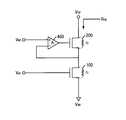
도1은 종래기술의 일예에 따른 캐스코드 스테이지이다.1 is a cascode stage according to an example of the prior art.
상기 도1을 참조하면, 종래 방식의 캐스코드 스테이지는 게이트단자에 바이어스 전압(VB2)이 인가되고 드레인단자가 출력이 Vo인 제 2 NMOS 트랜지스터(200)와, 상기 제 2 NMOS 트랜지스터(200)의 소오스단자와 드레인단자가 연결되며, 게이트단자에 바이어스 전압(VB1)이 인가되며 소오스단자가 접지된 제 1 NMOS 트랜지스터(100)로 구성된다.Referring to FIG. 1, a conventional cascode stage includes a
상기와 같이 구성된 종래기술의 캐스코드 스테이지에 있어서, 상기 제 1 NMOS 트랜지스터(100)의 소오스단자와 드레인단자 사이의 내부저항을 r1, 상기 제 2 NMOS 트랜지스터의 소오스단자와 드레인단자 사이의 내부저항을 r2, 그리고 상기 제 1,2 NMOS 트랜지스터(100,200)의 트랜스컨덕턴스를 각각 gm1, gm2라고 했을 경우, 제 2 NMOS 트랜지스터 (200)의 드레인에서 바라본 이 회로의 출력임피던스(R01)는 다음과 같다.
In the cascode stage of the prior art configured as described above, the internal resistance between the source terminal and the drain terminal of the
상기 제 1 수학식에 나타난 바와 같이, 상기 종래기술의 출력저항은 상기 제 1 NMOS 트랜지스터(100)의 내부저항(r1)과 상기 제 2 NMOS 트랜지스터(200)의 내부저항(r2)의 곱에 비례하며, 상기 제 2 NMOS 트랜지스터(200)의 트랜스컨덕턴스(gm2)에 의존한다.As the first shown in the first equation, the output resistance of the prior art is the product of the internal resistance (r2) of the first internal resistance of the NMOS transistor (100) (r1) and the first 2
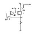
도2는 종래기술의 다른 예를 나타내는 캐스코드 스테이지이다.2 is a cascode stage showing another example of the prior art.
상기 도2를 참조하면, 상기 도 1의 구성에 제 2 NMOS 트랜지스터(200)의 소오스단자를 '-' 입력으로 하고, 바이어스 전압(VB2)을 '+' 입력으로 하는 반전증폭기(Inverting Amplifier)인 제 2 연산증폭기(400)를 부궤환 루프를 통해 상기 제 2 NMOS 트랜지스터(200)의 게이트단자의 입력으로 루프시킨 구성으로 이루어진다.Referring to FIG. 2, an inverting amplifier having a source terminal of the
상기와 같이 구성된 종래기술의 캐스코드 스테이지에 있어서, 상기 제 2 연산증폭기(400)의 증폭도를 A1이라고 했을 경우, 제 2 NMOS 트랜지스터(200)의 드레인에서 바라본 이 회로의 출력임피던스(R02)는 다음과 같다.
In the cascode stage of the prior art configured as described above, when the amplification degree of the second
상기 제 2 수학식에 나타난 바와 같이, 도 2에 도시된 캐스코드 스테이지의 출력임피던스는 상기 제 1 종래기술의 출력임피던스와 부궤환 루프로 연결된 제 2 연산증폭기(400)의 증폭도(A1)의 곱에 비례하며, 상기 제 2 NMOS 트랜지스터(200)의 트랜스컨덕턴스(gm2)에 의존한다.As shown in the second equation, the output impedance of the cascode stage shown in FIG. 2 is the amplification degree A1 of the second
상기 제 1,2 종래기술의 예에서, 제 1 종래기술은 상기 제 1 수학식에 나타난 바와 같이 큰 출력임피던스를 필요로 하는 증폭기, 비교기 및 에이디컨버터에서 출력임피던스가 낮은 문제가 발생한다. In the first and second prior art examples, the first prior art has a problem of low output impedance in an amplifier, a comparator and an AD converter which require a large output impedance as shown in the first equation.
제 1 종래기술에서의 문제점을 해결하기 위해 상기 제 2 종래기술에서는 상기 제 2 NMOS 트랜지스터(200)의 드레인단자에 반전증폭기인 제 2 연산증폭기(400)을 부궤환 루프를 통해 그 출력을 상기 제 2 NMOS 트랜지스터(200)의 게이트단자의 입력으로 루프시킴으로써, 상기 제 2 수학식에 나타난 바와 같이 출력임피던스가 제 2 연산증폭기(400)의 증폭도(A1)의 곱만큼 증가하도록 하였다. 그러나, 상기 제 1,2 종래기술보다 더 높은 출력임피던스를 얻기 위해 상기 제 1,2 종래기술의 캐스코드 스테이지를 직렬로 다단 연결했을 경우, 고출력임피던스는 얻을 수 있지만 출력전압의 스윙폭이 좁아지는 문제가 발생한다.
In order to solve the problem in the first conventional technology, in the second conventional technology, the output of the second
본 발명은 상기와 같은 종래 기술의 문제점을 해결하기 위하여 안출된 것으로서, 출력전압의 스윙 폭을 줄이지 않으면서 높은 출력임피던스를 얻기 위한 캐스코드 스테이지를 제공하는데 그 목적이 있다.SUMMARY OF THE INVENTION The present invention has been made to solve the problems of the prior art, and an object thereof is to provide a cascode stage for obtaining a high output impedance without reducing the swing width of the output voltage.
본 발명의 다른 목적은 공통게이트 증폭단에서 국부적으로 등가 트랜스컨덕턴스를 증가시키는데 적합한 캐스코드 증폭기를 제공하는데 있다.
Another object of the present invention is to provide a cascode amplifier suitable for increasing local equivalent transconductance in a common gate amplifier stage.
상기 목적을 달성하기 위하여 본 발명은 반도체메모리의 집적회로에 있어서, 제 1 바이어스 전압을 게이트단자에 입력하고 소오스단자는 접지된 제 1 NMOS 트랜지스터; 상기 제 1 NMOS 트랜지스터의 드레인단자의 출력을 '+' 입력으로 하고, 제 3 바이어스 전압을 '- 입력으로 하며, 부궤환 루프를 형성하여 비반전증폭기의 역할을 하는 제 1 연산증폭기; 상기 제 1 연산증폭기의 출력을 '- 입력으로 하고, 제 2 바이어스 전압을 '+' 입력으로 하며, 부궤환루프를 형성하여 반전증폭기의 역할을 하는 제 2 연산증폭기; 상기 제 2 연산증폭기의 출력을 게이트단자의 입력으로 하고, 상기 제 1 NMOS 트랜지스터의 드레인단자에 소오스단자가 연결되며 드레인단자가 출력단에 접속된 제 2 NMOS 트랜지스터를 포함하여 이루어진다.In order to achieve the above object, the present invention provides an integrated circuit of a semiconductor memory, comprising: a first NMOS transistor having a first bias voltage input to a gate terminal and a source terminal; A first operational amplifier configured to serve as a non-inverting amplifier by setting the output of the drain terminal of the first NMOS transistor as' + 'input, the third bias voltage as' − input, and forming a negative feedback loop; A second operational amplifier serving as an inverting amplifier by forming an output of the first operational amplifier as an '− input, a second bias voltage as an' + 'input, and forming a negative feedback loop; The output of the second operational amplifier is an input of a gate terminal, and a source terminal is connected to a drain terminal of the first NMOS transistor, and a drain terminal includes a second NMOS transistor connected to an output terminal.
이하, 본 발명이 속하는 기술분야에서 통상의 지식을 가진 자가 본 발명의 기술적 사상을 용이하게 실시할 수 있을 정도로 상세히 설명하기 위하여, 본 발명의 가장 바람직한 실시예를 첨부한 도면을 참조하여 설명하기로 한다.DETAILED DESCRIPTION Hereinafter, exemplary embodiments of the present invention will be described in detail with reference to the accompanying drawings so that those skilled in the art may easily implement the technical idea of the present invention. do.
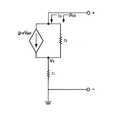
도3은 출력 단에 넓은 스윙 폭과 고출력임피던스를 제공하기 위한, 본 발명의 캐스코드 스테이지를 나타내는 상세 회로도이다.Figure 3 is a detailed circuit diagram illustrating the cascode stage of the present invention for providing a wide swing width and high output impedance at the output stage.
이하, 본 발명의 실시예에 대해서 상기 도3을 참조하면, 본 발명의 캐스코드 스테이지는 게이트단자에 제 1 바이어스 전압 VB1을 입력으로 하고 소오스단자가 접지된 제 1 NMOS 트랜지스터(100); 상기 제 1 NMOS 트랜지스터(100)의 드레인단자의 출력을 일 입력으로 하고, 제 3 바이어스 전압 VB3를 타 입력으로 하여 비반전증폭기의 역할을 하는 제 1 연산증폭기(300); 상기 제 1 연산증폭기(300)의 출력을 타 입력으로 하고, 제 2 바이어스 전압 VB2를 일 입력으로 하여 반전증폭기의 역할을 하는 제 2 연산증폭기(400); 상기 제 2 연산증폭기(400)의 출력을 게이트단자의 입력으로 하고, 상기 제 1 NMOS 트랜지스터(100)의 드레인단자에 소오스단자가 연결되며 드레인단자가 출력단에 접속된 제 2 NMOS 트랜지스터(200)를 포함하여 이루어진다.Hereinafter, referring to FIG. 3 for an embodiment of the present invention, the cascode stage of the present invention includes: a
여기서, 상기 제 1 NMOS 트랜지스터(100)는 내부저항이 r1이고, 내부 트랜스컨덕턴스가 gm1이며, 차동증폭기의 공통소오스 스테이지에서의 부하(Load)로서의 역할을 하여 출력전압 V03에 대한 출력전류 io에 대해 상기 내부저항(r1)과 같은 저항 성분으로서의 역할을 하며, 제 1 연산증폭기(300)는 상기 제 1 NMOS 트랜지스터의 드레인단자의 출력을 '+' 입력으로 하고 바이어스전압 VB3를 '-' 입력으로 하여 상기 입력에 증폭도 A2를 곱한 값을 출력으로 하는 부궤환루프를 형성하며 상기 제 1 연산증폭기(300)의 출력을 '-' 입력으로 하고 바이어스전압 VB2를 '+' 입력으로 하여 상기 입력에 증폭도 A1를 곱한 값을 출력으로 하는 부궤환루프를 형성하는 제 2 연산증폭기(400)와, 내부저항이 r2이고, 트랜스컨덕턴스가 gm2이고, 상기 제 2 연산증폭기(400)의 출력을 게이트단자의 입력으로 하고 소오스단자는 상기 제 1 NMOS 트랜지스터(100)의 드레인단자와 연결되며 드레인단자를 출력전압 Vo3로 하는 제 2 NMOS 트랜지스터(200)로 구성되어 있다.Here, the
도4는 상기 도 3의 출력전압(Vo3)을 구하기 위한 소신호모델(Small Signal Model)로서, 상기 도 3의 바이어스전압인 VB1,VB2,VB3를 생략하였으며, 상기 제 1 NMOS 트랜지스터(100)는 소신호 영역에서 보았을 경우 게이트단자의 전압이 상수이므로 내부저항과 동일한 r1으로 대체하였다. 또한, 제 2 NMOS 트랜지스터(200)의 소오스단자의 전압을 VS라 하면, 제 1 연산증폭기(300)의 출력전압은 상기 VS에 증폭 도 A2를 곱한 A2×VS가 되며, 상기 제 1 연산증폭기(300)의 출력을 입력으로 하는 제 2 연산증폭기(400)의 출력전압은 증폭도 A1을 곱한 -A1×A2×VS가 된다. 따라서, 상기 제 2 NMOS 트랜지스터(200)의 게이트전압 Vg2는 다음과 같다.
4 is a small signal model forobtaining the output voltage Vo3 of FIG. 3, and the bias voltages VB1 , VB2 and VB3 of FIG. 3 are omitted, and the first NMOS transistor is omitted. In the case of the small signal region (100), since the voltage at the gate terminal is a constant, it is replaced with r1 equal to the internal resistance. In addition, the second when a voltage of the source terminal of the NMOS transistor (200) VS referred to a first output voltage of the
도5는 상기 도 4에 대한 소신호등가회로(Small Signal Equivalent Circuits)이다.FIG. 5 is a small signal equivalent circuit of FIG. 4.
상기 도5를 참조하면, 상기 도 4의 제 2 NMOS 트랜지스터(200)는 전압제어전류원 gm2Vgs2와 소신호출력저항, 내부저항(r2)의 병렬연결로 대체되었으며, 상기 제 2 NMOS 트랜지스터(200)의 게이트단자와 소오스단자의 전압차인 Vgs2는 다음과 같다.
Referring to FIG. 5, the
여기에서, 상기 출력전압 Vo3에 흐르는 전류를 io라 하면, 상기 출력단자에서의 출력임피던스 Ro3는 옴의 법칙에 의해 다음과 같이 구할 수 있다.Here,assuming that the current flowing through the output voltage Vo3 is io , the output impedance Ro3 at the output terminal can be obtained by the Ohm's law as follows.
여기서, 상기 출력전류 io와 상기 내부저항 r1에 흐르는 전류는 동일하므로, 상기 제 2 NMOS 트랜지스터(200)의 소오스단자의 전압 VS는 다음과 같다.
Here, since the output current io and the current flowing in the internal resistance r1 are the same, the voltage VS of the source terminal of the
따라서, 상기 제 3,4,6 수학식에 의해 출력전압 Vo3는 다음과 같다.
Therefore, according to the third, fourth, and six equations, the output voltage Vo3 is as follows.
여기서, A1 ×A2(gm2 ×r2)r1의 값이r1+ r2+ (gm2 × r2)r1 보다 훨씬 크기 때문에 r1+ r2+ (gm2 × r2)r1는 무시할 수 있다. 따라서, 제 5,7 수학식에 의해 본 발명의 출력임피던스 Ro3는 다음과 같다.
Here, the value of A1 × A2 (gm2 × r2 ) r1 is Becauser 1 + r 2 + (g m2 × r 2) is much larger thanr 1 r 1 + r 2 + (g m2 × r 2)
상기 제 8 수학식에 도시된 바와 같이 본 발명의 출력임피던스는 상기 제 1 종래기술에 비해서는 A1 ×A2 배, 상기 제 2 종래기술에는 A2 배 증가하였음을 알 수 있다.The output impedance of the present invention as shown in the eighth equation it can be seen the first hayeoteum is A1 × A2 times, the second is A2-fold increase in the prior art as compared to the prior art.
도 3 내지 도 5를 참조하면, 도 3,4에서 상기 제 2 NMOS 트랜지스터(200)의 소스게이트가 출력전류 io의 변화를 감지하여 상기 제 2 NMSO(200)의 게이트단자로 부궤환루프를 통해 전달하게 된다. 따라서, 상기 제 2 NMOS 트랜지스터(200)의 등가 트랜스컨덕턴스(Equivalent Transconductance)는 음의 부호가 되어 상기 출력전류 io의 일부분을 상기 제 2 NMOS 트랜지스터(200)의 소스게이트에서 드레인게이트로 상기 출력전류 io와 역방향으로 내보내게 된다. 이 역방향전류는 결국, 상기 제 2 NMOS 트랜지스터(200)의 드레인게이트에서 합쳐지게 되므로 상기 출력전류 io를 감소시키는 결과가 되어 출력임피던스 Ro3는 증가하게 된다.3 to 5, in FIG. 3 and 4, the source gate of the
상술한 것처럼 본 발명의 캐스코드 스테이지는 부궤환루프에 비반전증폭기와 반전증폭기를 각각 직렬로 접속하므로써, 상기 제 1,2 종래기술에 비해 넓은 출력 스윙 폭과 높은 출력임피던스를 가짐을 실시예를 통해 알아보았다.As described above, the cascode stage of the present invention has a wider output swing width and a higher output impedance than the first and second prior arts by connecting the non-inverting amplifier and the inverting amplifier in series to the negative feedback loop. Learned through
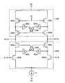
도 6은 본 발명의 다른 실시예를 나타내는 것으로서, 상기 도 3의 캐스코드 스테이지를 차동증폭기의 공통게이트 증폭단에 적용시킴으로써 등가 트랜스컨덕턴스를 국부적으로 증가시켜 위상 여유 스펙(Spec) 내에서 사용할 수 있도록 적용한 것이다.FIG. 6 illustrates another embodiment of the present invention, in which the cascode stage of FIG. 3 is applied to a common gate amplifier of the differential amplifier to locally increase an equivalent transconductance so that it can be used within a phase margin specification. will be.
도 6에 도시된 바와 같이, 차동증폭기는 500a 내지 500d의 네개의 PMOS 트랜지스터와 800a,b 두개의 연산증폭기 및 하나의 제 1 완전차동증폭기(700a)로 이루어진 제 1 차동증폭부(1000)와, 600a 내지 600d의 네개의 NMOS 트랜지스터와 800c,d의 두개의 연산증폭기 및 하나의 제 2 완전차동증폭기로 이루어지며, 전류원 Iss를 공통으로 갖고 공통소오스 스테이지를 형성하며, 게이트단자에 입력신호 Vi1과 Vi2가 각각 입력되는 상기 제 2,4 NMOS 트랜지스터(600b,d)로 이루어진 제 2 차동증폭부(2000)로 이루어진다.As shown in FIG. 6, the differential amplifier includes a first
상기와 같은 차동증폭기의 제 1 차동증폭부(1000)에서, 제 1 PMOS 트랜지스터(500a)와 제 2 PMOS 트랜지스터(500b)가 직렬 접속되고, 상기 제 1 PMOS 트랜지스터(500a)의 드레인단자에 제 1 연산증폭기(800a)와 제 1 완전차동증폭기(700a)가 부궤환 루프를 형성하여 상기 제 2 PMOS 트랜지스터(500b)의 게이트단자의 입력으로 루프되어 상기 제 1 연산증폭기(800a)의 증폭도 A3와 상기 제 1 차동증폭기(700a)의 증폭도 A5를 곱한만큼의 전압을 제 1 출력전압 Vo4에 전달한다. 따라서, 상기 제 1,2 PMOS 트랜지스터(500a,500b)와 상기 제 1 연산증폭기(800a) 및 상기 제 1 완전차동증폭기(700a)로 구성된 하나의 캐스코드 스테이지는 제 1 출력전압 Vo4에 상기 부궤환 루프를 통해 출력임피던스를 상기 제 1 연산증폭기(800a)의 증폭도 A3와 상기 제 1 차동증폭기(700a)의 증폭도 A5를 곱한만큼의 배로 증가시킨다. 한편, 제 3 PMOS 트랜지스터(500c)와 제 4 PMOS 트랜지스터(500d)가 직렬 접 속되고, 상기 제 3 PMOS 트랜지스터(500c)의 드레인단자에 제 2 연산증폭기(800b)와 상기 제 1 완전차동증폭기(700a)가 부궤환 루프를 형성하여 상기 제 4 PMOS 트랜지스터(500d)의 게이트단자의 입력으로 루프되어 상기 제 3 연산증폭기(800c)의 증폭도 A4와 상기 제 1 차동증폭기(700a)의 증폭도 A5를 곱한만큼의 전압을 제 2 출력전압 Vo5에 전달한다. 따라서, 상기 제 3,4 PMOS 트랜지스터(500c,500d)와 상기 제 3 연산증폭기(800c) 및 상기 제 1 완전차동증폭기(700a)로 구성된 하나의 캐스코드 스테이지는 제 2 출력전압 Vo5에 상기 부궤환 루프를 통해 출력임피던스를 상기 제 2 연산증폭기(800b)의 증폭도 A4와 상기 제 1 차동증폭기(700a)의 증폭도 A5를 곱한만큼의 배로 증가시킨다.In the first
상기와 같이 구성된 차동증폭기에서, 제 2 차동증폭부(2000)는 제 2 NMOS 트랜지스터(600b)와 제 4 NMOS 트랜지스터(600d)의 게이트단자에 두개의 입력 Vi1과 Vi2를 가해지면, 각 입력신호는 상기의 캐스코드 스테이지로 이루어진 증폭부를 거치면서 증폭이 되어 Vo4와 Vo5의 출력전압을 변화시키며, 상기 출력전압 Vo4와 Vo5의 변화에 의해 제 1 차동증폭부(1000)의 전류가 변동되어 또한, 상기의 캐스코드 스테이지로 이루어진 증폭부를 통해서 상기 제 2 증폭부(2000)의 출력과 동일한 출력을 각 Vo4, Vo5의 출력전압에 전달한다. 결국, Vo4와 Vo5의 출력전압은 제 1 차동증폭부 출력전압의 두배가 된다.In the differential amplifier configured as described above, when the second
따라서, 본 발명의 캐스코드 스테이지는 도 6에 도시된 차동증폭기에서 처럼 공통게이트 증폭단에서 국부적으로 등가 트랜스컨덕턴스를 크게 해야 할 필요가 있는 곳에서는 위상 여유 스펙(Spec) 내에서 사용할 수 있다.Therefore, the cascode stage of the present invention can be used within a phase margin specification where it is necessary to increase the local equivalent transconductance in the common gate amplifier stage as in the differential amplifier shown in FIG.
본 발명의 기술 사상은 상기 바람직한 실시예에 따라 구체적으로 기술되었으나, 상기한 실시예는 그 설명을 위한 것이며 그 제한을 위한 것이 아님을 주의하여야 한다. 또한, 본 발명의 기술 분야의 통상의 전문가라면 본 발명의 기술 사상의 범위내에서 다양한 실시예가 가능함을 이해할 수 있을 것이다.
Although the technical idea of the present invention has been described in detail according to the above preferred embodiment, it should be noted that the above-described embodiment is for the purpose of description and not of limitation. In addition, those skilled in the art will understand that various embodiments are possible within the scope of the technical idea of the present invention.
상기와 같이 본 발명은 증폭기의 캐스코드 스테이지의 부궤환 루프에 반전과 비반전 증폭기를 직렬 접속하여 출력단에 고출력임피던스를 제공하고, 출력전압의 스윙 폭을 넓게 할 수 있도록 한다.As described above, the present invention provides a high output impedance to the output terminal by connecting an inverting and non-inverting amplifier in series to the negative feedback loop of the cascode stage of the amplifier, and widens the swing width of the output voltage.
Claims (3)
Translated fromKoreanPriority Applications (1)
| Application Number | Priority Date | Filing Date | Title |
|---|---|---|---|
| KR1020000063183AKR100658922B1 (en) | 2000-10-26 | 2000-10-26 | Cascode stages with improved output impedance and cascode amplifiers using them |
Applications Claiming Priority (1)
| Application Number | Priority Date | Filing Date | Title |
|---|---|---|---|
| KR1020000063183AKR100658922B1 (en) | 2000-10-26 | 2000-10-26 | Cascode stages with improved output impedance and cascode amplifiers using them |
Publications (2)
| Publication Number | Publication Date |
|---|---|
| KR20020032170A KR20020032170A (en) | 2002-05-03 |
| KR100658922B1true KR100658922B1 (en) | 2006-12-15 |
Family
ID=19695561
Family Applications (1)
| Application Number | Title | Priority Date | Filing Date |
|---|---|---|---|
| KR1020000063183AExpired - LifetimeKR100658922B1 (en) | 2000-10-26 | 2000-10-26 | Cascode stages with improved output impedance and cascode amplifiers using them |
Country Status (1)
| Country | Link |
|---|---|
| KR (1) | KR100658922B1 (en) |
Families Citing this family (3)
| Publication number | Priority date | Publication date | Assignee | Title |
|---|---|---|---|---|
| KR101163457B1 (en) | 2006-02-24 | 2012-07-18 | 삼성전자주식회사 | Low Voltage Regulated Cascade Circuits and CMOS Analog Circuits |
| KR101438829B1 (en)* | 2008-07-25 | 2014-09-05 | 엘지이노텍 주식회사 | Actuator driver |
| KR101393932B1 (en)* | 2011-12-08 | 2014-05-12 | 진옥상 | Small signal buffer amplification circuit |
Citations (5)
| Publication number | Priority date | Publication date | Assignee | Title |
|---|---|---|---|---|
| US4442410A (en)* | 1981-10-29 | 1984-04-10 | Halliburton Company | Temperature stabilized amplifier for borehole use |
| US5166635A (en)* | 1991-03-27 | 1992-11-24 | Level One Communications, Inc. | Digital data line driver |
| JPH05199044A (en)* | 1992-01-22 | 1993-08-06 | Nec Ic Microcomput Syst Ltd | Pulse width modulation amplifier circuit |
| KR960009388A (en)* | 1994-08-25 | 1996-03-22 | 프레데릭 얀 스미트 | Power follower of voltage follower type |
| US5789981A (en)* | 1996-04-26 | 1998-08-04 | Analog Devices, Inc. | High-gain operational transconductance amplifier offering improved bandwidth |
- 2000
- 2000-10-26KRKR1020000063183Apatent/KR100658922B1/ennot_activeExpired - Lifetime
Patent Citations (5)
| Publication number | Priority date | Publication date | Assignee | Title |
|---|---|---|---|---|
| US4442410A (en)* | 1981-10-29 | 1984-04-10 | Halliburton Company | Temperature stabilized amplifier for borehole use |
| US5166635A (en)* | 1991-03-27 | 1992-11-24 | Level One Communications, Inc. | Digital data line driver |
| JPH05199044A (en)* | 1992-01-22 | 1993-08-06 | Nec Ic Microcomput Syst Ltd | Pulse width modulation amplifier circuit |
| KR960009388A (en)* | 1994-08-25 | 1996-03-22 | 프레데릭 얀 스미트 | Power follower of voltage follower type |
| US5789981A (en)* | 1996-04-26 | 1998-08-04 | Analog Devices, Inc. | High-gain operational transconductance amplifier offering improved bandwidth |
Also Published As
| Publication number | Publication date |
|---|---|
| KR20020032170A (en) | 2002-05-03 |
Similar Documents
| Publication | Publication Date | Title |
|---|---|---|
| US6717474B2 (en) | High-speed differential to single-ended converter | |
| JP3584067B2 (en) | Improved gain enhancement method for operational amplifiers | |
| TWI321900B (en) | Differential amplifier and semiconductor circuit | |
| JPH0360209A (en) | Amplifier circuit and semiconductor integrated circuit including the same | |
| US20080106336A1 (en) | Differential amplifier with current source controlled through differential feedback | |
| EP0286347B1 (en) | Balanced output analog differential amplifier circuit | |
| US8169263B2 (en) | Differential gm-boosting circuit and applications | |
| US6469576B2 (en) | Amplifier circuit for a physical random number generator and a random number generator using the same | |
| US7215199B2 (en) | Method and system for simplifying common mode feedback circuitry in multi-stage operational amplifiers | |
| US6525608B2 (en) | High gain, high bandwidth, fully differential amplifier | |
| US6545502B1 (en) | High frequency MOS fixed and variable gain amplifiers | |
| JP2004222015A (en) | Amplifier circuit | |
| EP1124327A1 (en) | Differential amplifier with gain substantially independent of temperature | |
| KR100658922B1 (en) | Cascode stages with improved output impedance and cascode amplifiers using them | |
| US11199564B2 (en) | Current sensing circuit | |
| US5337007A (en) | High efficiency class AB transconductance amplifier | |
| US6072339A (en) | Current sensing circuit with high input impedance | |
| JPH08242130A (en) | Operational Transconductance Amplifier | |
| JP2007505585A (en) | Improvements in and related to transconductor circuits | |
| JP2005080090A (en) | Output voltage control circuit of differential amplifier circuit and voltage detector | |
| JPH06216662A (en) | Phase compensation circuit for amplifier | |
| JPH08307224A (en) | Operational amplifier circuit | |
| JP3685118B2 (en) | CMOS inverter circuit and DC offset detection circuit | |
| US6407637B1 (en) | Differential current mirror and method | |
| US20240421771A1 (en) | Electrical circuit, single-ended amplifier, and operating method of an electrical circuit |
Legal Events
| Date | Code | Title | Description |
|---|---|---|---|
| PA0109 | Patent application | Patent event code:PA01091R01D Comment text:Patent Application Patent event date:20001026 | |
| PG1501 | Laying open of application | ||
| N231 | Notification of change of applicant | ||
| PN2301 | Change of applicant | Patent event date:20041006 Comment text:Notification of Change of Applicant Patent event code:PN23011R01D | |
| A201 | Request for examination | ||
| PA0201 | Request for examination | Patent event code:PA02012R01D Patent event date:20050203 Comment text:Request for Examination of Application Patent event code:PA02011R01I Patent event date:20001026 Comment text:Patent Application | |
| E902 | Notification of reason for refusal | ||
| PE0902 | Notice of grounds for rejection | Comment text:Notification of reason for refusal Patent event date:20060628 Patent event code:PE09021S01D | |
| E701 | Decision to grant or registration of patent right | ||
| PE0701 | Decision of registration | Patent event code:PE07011S01D Comment text:Decision to Grant Registration Patent event date:20061204 | |
| GRNT | Written decision to grant | ||
| PR0701 | Registration of establishment | Comment text:Registration of Establishment Patent event date:20061211 Patent event code:PR07011E01D | |
| PR1002 | Payment of registration fee | Payment date:20061211 End annual number:3 Start annual number:1 | |
| PG1601 | Publication of registration | ||
| PR1001 | Payment of annual fee | Payment date:20091117 Start annual number:4 End annual number:4 | |
| PR1001 | Payment of annual fee | Payment date:20101122 Start annual number:5 End annual number:5 | |
| PR1001 | Payment of annual fee | Payment date:20111124 Start annual number:6 End annual number:6 | |
| FPAY | Annual fee payment | Payment date:20121121 Year of fee payment:7 | |
| PR1001 | Payment of annual fee | Payment date:20121121 Start annual number:7 End annual number:7 | |
| FPAY | Annual fee payment | Payment date:20131118 Year of fee payment:8 | |
| PR1001 | Payment of annual fee | Payment date:20131118 Start annual number:8 End annual number:8 | |
| FPAY | Annual fee payment | Payment date:20141119 Year of fee payment:9 | |
| PR1001 | Payment of annual fee | Payment date:20141119 Start annual number:9 End annual number:9 | |
| FPAY | Annual fee payment | Payment date:20151118 Year of fee payment:10 | |
| PR1001 | Payment of annual fee | Payment date:20151118 Start annual number:10 End annual number:10 | |
| FPAY | Annual fee payment | Payment date:20161118 Year of fee payment:11 | |
| PR1001 | Payment of annual fee | Payment date:20161118 Start annual number:11 End annual number:11 | |
| FPAY | Annual fee payment | Payment date:20171117 Year of fee payment:12 | |
| PR1001 | Payment of annual fee | Payment date:20171117 Start annual number:12 End annual number:12 | |
| FPAY | Annual fee payment | Payment date:20181120 Year of fee payment:13 | |
| PR1001 | Payment of annual fee | Payment date:20181120 Start annual number:13 End annual number:13 | |
| FPAY | Annual fee payment | Payment date:20191119 Year of fee payment:14 | |
| PR1001 | Payment of annual fee | Payment date:20191119 Start annual number:14 End annual number:14 | |
| PC1801 | Expiration of term | Termination date:20210426 Termination category:Expiration of duration |