KR100658857B1 - Thermal CD of TAN film from tantalum halide precursor - Google Patents
Thermal CD of TAN film from tantalum halide precursorDownload PDFInfo
- Publication number
- KR100658857B1 KR100658857B1KR1020017013564AKR20017013564AKR100658857B1KR 100658857 B1KR100658857 B1KR 100658857B1KR 1020017013564 AKR1020017013564 AKR 1020017013564AKR 20017013564 AKR20017013564 AKR 20017013564AKR 100658857 B1KR100658857 B1KR 100658857B1
- Authority
- KR
- South Korea
- Prior art keywords
- tantalum
- precursor
- tan
- vapor
- temperature
- Prior art date
- Legal status (The legal status is an assumption and is not a legal conclusion. Google has not performed a legal analysis and makes no representation as to the accuracy of the status listed.)
- Expired - Fee Related
Links
Images


Classifications
- H01L21/205—
- H—ELECTRICITY
- H01—ELECTRIC ELEMENTS
- H01L—SEMICONDUCTOR DEVICES NOT COVERED BY CLASS H10
- H01L21/00—Processes or apparatus adapted for the manufacture or treatment of semiconductor or solid state devices or of parts thereof
- H01L21/70—Manufacture or treatment of devices consisting of a plurality of solid state components formed in or on a common substrate or of parts thereof; Manufacture of integrated circuit devices or of parts thereof
- H01L21/71—Manufacture of specific parts of devices defined in group H01L21/70
- H01L21/768—Applying interconnections to be used for carrying current between separate components within a device comprising conductors and dielectrics
- H01L21/76838—Applying interconnections to be used for carrying current between separate components within a device comprising conductors and dielectrics characterised by the formation and the after-treatment of the conductors
- H01L21/76841—Barrier, adhesion or liner layers
- H01L21/76843—Barrier, adhesion or liner layers formed in openings in a dielectric
- C—CHEMISTRY; METALLURGY
- C23—COATING METALLIC MATERIAL; COATING MATERIAL WITH METALLIC MATERIAL; CHEMICAL SURFACE TREATMENT; DIFFUSION TREATMENT OF METALLIC MATERIAL; COATING BY VACUUM EVAPORATION, BY SPUTTERING, BY ION IMPLANTATION OR BY CHEMICAL VAPOUR DEPOSITION, IN GENERAL; INHIBITING CORROSION OF METALLIC MATERIAL OR INCRUSTATION IN GENERAL
- C23C—COATING METALLIC MATERIAL; COATING MATERIAL WITH METALLIC MATERIAL; SURFACE TREATMENT OF METALLIC MATERIAL BY DIFFUSION INTO THE SURFACE, BY CHEMICAL CONVERSION OR SUBSTITUTION; COATING BY VACUUM EVAPORATION, BY SPUTTERING, BY ION IMPLANTATION OR BY CHEMICAL VAPOUR DEPOSITION, IN GENERAL
- C23C16/00—Chemical coating by decomposition of gaseous compounds, without leaving reaction products of surface material in the coating, i.e. chemical vapour deposition [CVD] processes
- C23C16/22—Chemical coating by decomposition of gaseous compounds, without leaving reaction products of surface material in the coating, i.e. chemical vapour deposition [CVD] processes characterised by the deposition of inorganic material, other than metallic material
- C23C16/30—Deposition of compounds, mixtures or solid solutions, e.g. borides, carbides, nitrides
- C23C16/34—Nitrides
- H—ELECTRICITY
- H01—ELECTRIC ELEMENTS
- H01L—SEMICONDUCTOR DEVICES NOT COVERED BY CLASS H10
- H01L21/00—Processes or apparatus adapted for the manufacture or treatment of semiconductor or solid state devices or of parts thereof
- H01L21/02—Manufacture or treatment of semiconductor devices or of parts thereof
- H01L21/04—Manufacture or treatment of semiconductor devices or of parts thereof the devices having potential barriers, e.g. a PN junction, depletion layer or carrier concentration layer
- H01L21/18—Manufacture or treatment of semiconductor devices or of parts thereof the devices having potential barriers, e.g. a PN junction, depletion layer or carrier concentration layer the devices having semiconductor bodies comprising elements of Group IV of the Periodic Table or AIIIBV compounds with or without impurities, e.g. doping materials
- H01L21/28—Manufacture of electrodes on semiconductor bodies using processes or apparatus not provided for in groups H01L21/20 - H01L21/268
- H01L21/283—Deposition of conductive or insulating materials for electrodes conducting electric current
- H01L21/285—Deposition of conductive or insulating materials for electrodes conducting electric current from a gas or vapour, e.g. condensation
- H01L21/28506—Deposition of conductive or insulating materials for electrodes conducting electric current from a gas or vapour, e.g. condensation of conductive layers
- H01L21/28512—Deposition of conductive or insulating materials for electrodes conducting electric current from a gas or vapour, e.g. condensation of conductive layers on semiconductor bodies comprising elements of Group IV of the Periodic Table
- H01L21/28556—Deposition of conductive or insulating materials for electrodes conducting electric current from a gas or vapour, e.g. condensation of conductive layers on semiconductor bodies comprising elements of Group IV of the Periodic Table by chemical means, e.g. CVD, LPCVD, PECVD, laser CVD
Landscapes
- Chemical & Material Sciences (AREA)
- Engineering & Computer Science (AREA)
- Computer Hardware Design (AREA)
- Microelectronics & Electronic Packaging (AREA)
- General Chemical & Material Sciences (AREA)
- Condensed Matter Physics & Semiconductors (AREA)
- General Physics & Mathematics (AREA)
- Manufacturing & Machinery (AREA)
- Chemical Kinetics & Catalysis (AREA)
- Physics & Mathematics (AREA)
- Power Engineering (AREA)
- Inorganic Chemistry (AREA)
- Materials Engineering (AREA)
- Mechanical Engineering (AREA)
- Metallurgy (AREA)
- Organic Chemistry (AREA)
- Chemical Vapour Deposition (AREA)
- Electrodes Of Semiconductors (AREA)
Abstract
Translated fromKoreanDescription
Translated fromKorean본 발명은 집적 회로의 형성에 관한 것으로서, 특히, 할로겐화 탄탈 전구 물질로부터의 질화 탄탈 막의 화학 증착에 관한 것이다.FIELD OF THE INVENTION The present invention relates to the formation of integrated circuits and, in particular, to the chemical vapor deposition of tantalum nitride films from tantalum halide precursors.
집적 회로는 전기 장치에서 신호 전달을 위한 경로를 제공한다. 장치 내의 IC는 반도체 기질(substrate)의 규소 베이스 층 내에 포함된 다수의 활성 트랜지스터로 구성된다. IC의 용량을 증대하기 위해, 금속 "와이어"에 의한 다수의 상호 접속(interconnections)은, 기질의 규소 베이스 내의 한 활성 트랜지스터와 기질의 규소 베이스 내의 다른 활성 트랜지스터 사이에서 행해진다. 총체적으로 회로의 금속 상호 접속으로 공지된 상호 접속은 기질 내에 있는 홀(hole), 비아(via) 또는 트렌치를 통해 행해진다. 규소 베이스와 실제로 접촉하는 금속 상호 접속의 특정 포인트는 접점으로 공지되어 있다. 홀, 비아 또는 트렌치의 나머지는 접점 플러그라 칭하는 도전성 재료로 충진(fill)된다. 트랜지스터 밀도가 계속 증가하여, 고 레벨의 집적 회로를 형성함에 따라, 접점 플러그의 직경은 상호 접속부, 다단(multilevel) 금속화 구조체 및 고 종횡비 비아의 수를 증대시키도록 감소해야 한다.Integrated circuits provide a path for signal transmission in electrical devices. The IC in the device consists of a number of active transistors contained within a silicon base layer of a semiconductor substrate. In order to increase the capacity of the IC, a number of interconnections by metal "wires" are made between one active transistor in the silicon base of the substrate and the other active transistor in the silicon base of the substrate. The interconnect, collectively known as the metal interconnect of the circuit, is done through holes, vias or trenches in the substrate. A particular point of the metal interconnect that actually contacts the silicon base is known as the contact. The rest of the holes, vias or trenches are filled with a conductive material called contact plugs. As transistor densities continue to increase to form high level integrated circuits, the diameter of the contact plug must decrease to increase the number of interconnects, multilevel metallization structures, and high aspect ratio vias.
알루미늄은 집적 회로 내의 접점 및 상호 접속부에 허용된 표준이었다. 그러나, 전자 이동(electromigration) 및 고 전기 저항률에 따른 문제에 의해, 서브미크론(submicron)의 크기를 가진 새로운 구조체에 대한 새로운 재료가 필요하게 된다. 구리는, 초대규모 집적(ULSI) 회로의 차세대 집적 회로를 위한 상호 접속 재료로서 유망하지만, 저온에서의 구리 규화물(Cu-Si) 화합물의 형성 및, 산화 규소(SiO2)를 통한 전자 이동은 이것을 사용할 시에 결점이 있다.Aluminum was the accepted standard for contacts and interconnects in integrated circuits. However, due to the problems of electromigration and high electrical resistivity, new materials for new structures with submicron sizes are needed. Copper is promising as an interconnect material for the next generation of integrated circuits of ultra-large scale integrated (ULSI) circuits, but the formation of copper silicide (Cu-Si) compounds at low temperatures and electron transfer through silicon oxide (SiO2 ) There is a flaw in use.
상호 접속 소자의 선택으로서 알루미늄에서 구리로 전환할 시에, 기질의 하부(underlying) 유전체 층으로의 구리 확산을 방지하는 장벽으로서 역할을 하고, 후속 구리 증착을 위한 효과적인 "접착제(glue)" 층을 형성하는 새로운 재료가 필요하다. 또한. 후속 증착된 구리를 기질에 부착하는 라이너(liner)로서 역할을 하는 새로운 재료가 필요하다. 라이너는 또한 구리와 장벽 재료 사이에 저 전기 저항의 인터페이스를 제공한다. 스퍼터링과 같은 물리적 증착(PVD)법 및/또는 화학 증착(CVD)법에 의해 증착된 티탄(Ti) 및 질화 티탄(TiN) 장벽층과 같이, 이전에 알루미늄과 함께 사용된 장벽층은 구리에 대한 장벽으로서 비효율적이다. 게다가, Ti는, PVD 및/또는 CVD에 이용된 비교적 저온에서 구리 티탄 화합물을 형성하도록 구리와 반응한다.When switching from aluminum to copper as the choice of interconnect device, it acts as a barrier to prevent copper diffusion into the underlying dielectric layer of the substrate and provides an effective "glue" layer for subsequent copper deposition. New materials are needed to form. Also. There is a need for a new material that serves as a liner that attaches subsequent deposited copper to a substrate. The liner also provides an interface of low electrical resistance between the copper and the barrier material. Barriers previously used with aluminum, such as titanium (Ti) and titanium nitride (TiN) barrier layers deposited by physical vapor deposition (PVD) and / or chemical vapor deposition (CVD), such as sputtering, It is inefficient as a barrier. In addition, Ti reacts with copper to form copper titanium compounds at relatively low temperatures used in PVD and / or CVD.
스퍼터된 탄탈(Ta) 및 반응 스퍼터된 질화 탄탈(TaN)은, 고 전도도, 고 열 안정성 및 이종 원자의 확산에 대한 저항성으로 인해 구리와 규소 기질 간의 양호한 확산 장벽인 것으로 입증되었다. 그러나, 증착된 Ta 및/또는 TaN 막은 차폐(shadowing) 효과로 인해 스텝 커버리지(step coverage)가 본래대로 되지 않는다. 따라서, 스퍼터링법은 비교적 큰 특징물(feature) 사이즈 (> 0.3 ㎛) 및 작은 종횡비 접점 비아로 제한된다. CVD는, 고 종횡비를 가진 작은 구조체(< 0.25 ㎛)에서도, 양호한 등각성(conformality)의 PVD에 고유 이점을 제공한다. 그러나, 3급 부틸이미도트리스(디에틸아미도)탄탈(TBTDET), 펜타키스(디메틸아미도)탄탈(PDMAT) 및 펜타키스(디에틸아미도)탄탈(PDEAT)와 같은 금속-유기원을 이용한 Ta 및 TaN의 CVD는 잡다한 결과를 초래한다. Ta 및 TaN에 따른 부가적인 문제는, 생성된 모든 막이 비교적 고 농도의 산소 및 탄소 불순물을 가지고, 담체 가스를 사용할 필요가 있다.Sputtered tantalum (Ta) and reactive sputtered tantalum nitride (TaN) have proven to be good diffusion barriers between copper and silicon substrates due to their high conductivity, high thermal stability and resistance to diffusion of heteroatoms. However, the deposited Ta and / or TaN film does not have step coverage due to the shadowing effect. Thus, sputtering methods are limited to relatively large feature sizes (> 0.3 μm) and small aspect ratio contact vias. CVD offers inherent advantages to PVD of good conformality, even with small structures with high aspect ratios (<0.25 μm). However, metal-organic sources such as tertiary butylimidotris (diethylamido) tantalum (TBTDET), pentakis (dimethylamido) tantalum (PDMAT) and pentakis (diethylamido) tantalum (PDEAT) CVD of Ta and TaN has miscellaneous results. An additional problem with Ta and TaN is that all the resulting films have relatively high concentrations of oxygen and carbon impurities and it is necessary to use carrier gases.
담체 가스를 사용할 필요가 있다는 것은 담체 내의 전구 물질 가스의 농도가 정확히 알려지지 않은 결점을 갖는다. 결과적으로, 담체 가스 및 전구 물질 가스의 혼합물을 CVD 반응실로 정확히 계량하여도, 반응기로 전구 물질 가스 단독의 정확한 계량을 확실하게 하지 않는다. 이것은 CVD 실 내의 반응물이 과다하거나 너무 적게 할 수 있다. 담체 가스를 사용한다는 것은 또한 흐르는 담체 가스에 의해 미립자가 자주 픽업되어, 오염물로서 CVD 반응실로 송출되는 결점을 갖는다. 처리 동안 반도체 웨이퍼의 표면상에 입자가 존재하면, 결과적으로 결함있는 반도체 장치를 제조할 수 있다.The need to use a carrier gas has the drawback that the concentration of precursor gas in the carrier is not known exactly. As a result, even accurate metering of the mixture of carrier gas and precursor gas into the CVD reaction chamber does not ensure accurate metering of the precursor gas alone into the reactor. This may result in excessive or too little reactant in the CVD chamber. The use of a carrier gas also has the drawback that the particulates are frequently picked up by the flowing carrier gas and sent out to the CVD reaction chamber as contaminants. The presence of particles on the surface of the semiconductor wafer during processing can result in the production of defective semiconductor devices.
따라서, 열 CVD법에 의해 TaN을 증착하는 방법은 차세대 IC에서 구리 장벽을 형성할 시에 이점을 제공한다. 이상적으로, 증착된 막은 고 스텝 커버리지(특징물의 바닥부에서의 코팅 두께 대 특징물의 측면 또는, 특징물에 인접한 기질 또는 웨이퍼의 상부 표면 상의 두께의 비), 양호한 확산 장벽성, 최소 불순물, 저 저항률, 양호한 등각성(고 종횡비의 특징물의 복잡한 토포그래피의 균일한 커버리지)을 가지며, 이상적으로 이 방법은 고 증착 속도를 가진다.Thus, the method of depositing TaN by thermal CVD provides an advantage in forming copper barriers in next generation ICs. Ideally, the deposited film has a high step coverage (ratio of coating thickness at the bottom of the feature to the side of the feature or on the top surface of the substrate or wafer adjacent to the feature), good diffusion barrier properties, minimal impurities, low resistivity , Good conformality (even coverage of complex topography of high aspect ratio features), ideally this method has a high deposition rate.
본 발명은 질화 탄탈(TaN×) 막을 할로겐화 탄탈 전구 물질로부터 기질 상에 증착하는 방법에 관한 것이다. 할로겐화 탄탈 전구 물질은, 상기 전구 물질을 기화시켜, 탄탈 증기를 기질을 포함한 반응실로 송출하기 위한 기화 압력을 제공하기에 충분한 온도로 전구 물질을 가열함으로써 담체 가스없이 송출된다. 이 기화 압력은 약 3 Torr(399.97 N/㎡)보다 큰 것이 바람직하다. 증기는 질소를 함유한 처리 가스와 조합되고, TaN×는 열 화학 증착 (CVD)법에 의해 기질 상에 증착된다. 할로겐화 탄탈 전구 물질은, 불화 탄탈(TaF), 염화 탄탈(TaCl) 또는 브롬화 탄탈(TaBr), 바람직하게는 펜타불화 탄탈(TaF5), 펜타염화 탄탈(TaCl5) 또는 펜타브롬화 탄탈(TaBr5)일 수 있다. 기질 온도는 약 300℃-500℃의 범위 내에 있는 것이 바람직하다.The present invention relates to a method for depositing a tantalum nitride (TaNx ) film from a tantalum halide precursor. The tantalum halide precursor is delivered without carrier gas by heating the precursor to a temperature sufficient to vaporize the precursor and provide a vaporization pressure for delivering tantalum vapor to the reaction chamber containing the substrate. This vaporization pressure is preferably greater than about 3 Torr (399.97 N / m 2). The vapor is combined with a processing gas containing nitrogen and TaNx is deposited on the substrate by thermal chemical vapor deposition (CVD). Halogenated tantalum precursor fluoride, tantalum (TaF), chloride, tantalum (TaCl) or bromide, tantalum (TaBr), preferably a penta-fluoride tantalum (TaF5), penta-chloride, tantalum (TaCl5) or penta-bromide, tantalum (TaBr5) Can be. The substrate temperature is preferably in the range of about 300 ° C-500 ° C.
삭제delete
삭제delete
삭제delete
본 발명에 따라 증착된 TaN×층은 최소 불순물 및 저 저항률을 갖는다. 이 막은 양호한 스텝 커버리지, 고 종횡비의 특징물의 양호한 등각성을 제공하고, 구리 막에 대해 양호한 확산 장벽이다.The TaNx layer deposited according to the present invention has minimal impurities and low resistivity. This film provides good step coverage, good conformality of high aspect ratio features, and is a good diffusion barrier for copper films.
본 발명의 개시된 방법 및 기질은 일련의 용도를 갖는 것으로 이해된다. 이런 및 다른 이점은 다음의 도면 및 상세한 설명을 참조로 더욱 이해될 수 있다.It is understood that the disclosed methods and substrates have a series of uses. These and other advantages can be further understood with reference to the following figures and detailed description.
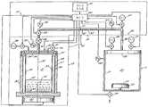
도 1은 열 화학 증착(CVD)용 장치의 개략도이다.1 is a schematic diagram of an apparatus for thermal chemical vapor deposition (CVD).
도 2는 할로겐화 탄탈(Ta)의 증기압 대 온도의 그래프이다.2 is a graph of vapor pressure versus temperature of tantalum halide (Ta).
도 3은 펜타불화 탄탈(TaF5) 전구 물질을 이용하여 증착된 질화 탄탈(TaN×) 막의 주사 전자 현미경(SEM)의 사진이다.3 is a photograph of a scanning electron microscope (SEM) of a tantalum nitride (TaNx ) film deposited using a tantalum fluoride (TaF5 ) precursor.
도 4는 펜타브롬화 탄탈(TaBr5) 전구 물질을 이용하여 증착된 TaN× 막의 SEM의 사진이다.4 is a SEM photograph of a TaNx film deposited using a tantalum pentabromide (TaBr5 ) precursor.
도 5는 구리층 상에 증착된 TaBr5 전구 물질을 이용하여 증착된 TaN× 막의 오거(Auger) 스펙트럼 트레이싱(tracing)이다.FIG. 5 is Auger spectral tracing of TaN× film deposited using TaBr5 precursor deposited on the copper layer.
탄탈(Ta)과 같은 내화성의 전이 금속 및 이들의 질화물막(TaN)은 구리(Cu)에 대해 유효한 확산 장벽이다. 이들의 유효성은, 이들의 고 열 안정성, 고 전도도 및, 이종 원소 또는 불순물의 확산에 대한 저항성에 기인한다. Ta 및 TaN은 특히 Cu와 이들의 화학적 불활성에 때문에 장점이 있고, Cu와 Ta 또는 Cu와 N 사이에서 어떤 화합물도 생성하지 않는다.Refractory transition metals such as tantalum (Ta) and their nitride films (TaN) are effective diffusion barriers for copper (Cu). Their effectiveness is due to their high thermal stability, high conductivity and resistance to diffusion of heterogeneous elements or impurities. Ta and TaN are particularly advantageous because of their Cu and their chemical inertness and do not produce any compound between Cu and Ta or Cu and N.
할로겐화 탄탈은 Ta 및 TaN을 위한 편리한 무기원을 제공한다. 특히, 무기 전구 물질은 펜타할로겐화 탄탈(TaX5)인데, 여기서, X는 할라이드 불소(F), 염소(Cl) 및 브롬(Br)을 나타낸다. 표 1은, 할로겐화 탄탈 전구 물질, 특히, 펜타불화 탄탈(TaF5), 펜타염화 탄탈(TaCl5) 및 펜타브롬화 탄탈(TaBr5)의 관련 열역학적 성질을 나타내고, 비교를 위해 펜타요오드화 탄탈(TaI5)이 포함된다. TaF5, TaCl5 및 TaBr5전구 물질 재료는 모두 실온(18℃-22℃)에서 고체이다.Tantalum halides provide a convenient inorganic source for Ta and TaN. In particular, the inorganic precursor is tantalum pentahalide (TaX5 ), where X represents halide fluorine (F), chlorine (Cl) and bromine (Br). Table 1, the halogenated tantalum precursor, in particular penta-fluoride tantalum (TaF5), penta-chloride, tantalum (TaCl5) and penta-bromide, tantalum penta-iodide tantalum For comparison indicates a related thermodynamic properties, the (TaBr5) (TaI5 ) Is included. TaF5 , TaCl5 and TaBr5 precursor materials are all solid at room temperature (18 ° C.-22 ° C.).
표 1 Table 1
화학 증착(CVD)법에서, 가스 전구 물질은 열 에너지 또는 전기 에너지를 이용하여 활성화된다. 활성화할 시에, 가스 전구 물질은 화학적으로 반응하여 막을 형성한다. 바람직한 CVD법은, 도 1에 도시되고, 웨스텐도프(Westendorp) 등에 의해, 본원과 동일자로 출원되고, 도쿄 일렉트론 리미티드에게 양도된 명칭이 APPARATUS AND METHOD FOR DELIVERY OF VAPOR FROM SOLID SOURCES TO A CVD CHAMBER인 계류 중인 출원에 개시되어 있다. 화학 증착(CVD) 시스템(10)은 CVD 반응실(11) 및 전구 물질 송출(delivery) 시스템(12)을 포함한다. 반응실(11)에서, 반응을 행하여, 예컨대, 염화 탄탈(TaCl) 또는 다른 할로겐화 탄탈 화합물의 전구 물질 가스를 탄탈(Ta) 또는 질화 탄탈(TaNX)의 장벽층 막과 같은 막으로 변화시킨다. TaN 막은 특정 화학양론성(stoichiometry)(TaNX)으로 제한되지 않는데, 그 이유는 TaNX가 주어진 증착에서 가스의 비율을 변화시킴으로써 연속적으로 변화될 수 있기 때문이다. 따라서, 여기서 이용된 바와 같이, TaNX는 어떤 화학양론성의 질화 탄탈 막을 포함한다.In chemical vapor deposition (CVD), gas precursors are activated using thermal or electrical energy. Upon activation, the gas precursor reacts chemically to form a film. A preferred CVD method is shown in FIG. 1, filed under the same application as in the present application by Westendorp et al., And assigned to Tokyo Electron Limited, which is named APPARATUS AND METHOD FOR DELIVERY OF VAPOR FROM SOLID SOURCES TO A CVD CHAMBER. A pending application is disclosed. The chemical vapor deposition (CVD)
전구 물질 송출 시스템(12)은 가스 출구(14)를 가진 전구 물질 가스원(13)을 포함하며, 가스 출구(14)는 가스 입구(16)를 가진 계량 시스템(15)을 통해 CVD 반응실(11)로 통한다. 가스원(13)은 할로겐화 탄탈 화합물로부터 전구 물질 증기, 예컨대, 할로겐화 탄탈 증기를 생성시킨다. 이 화합물은 표준 온도 및 압력에서 고체 상태로 있는 것이다. 전구 물질원은, 바람직하게는 제어된 가열에 의해, 전구 물질의 원하는 증기압을 생성시키는 온도로 유지된다. 증기압은, 담체 가스를 사용하지 않고, 전구 물질 증기를 반응실(11)로 송출하는데 충분한 것이다. 계량 시스템(15)은, 반응기(11) 내에 상업적으로 실행 가능한(viable) CVD법을 유지하는데 충분한 속도로, 가스원(13)에서 반응실(11)로 전구 물질 가스 증기의 흐름을 유지한다.
반응실(11)은 일반적으로 통상의 CVD 반응기이고, 완전한 진공(vacuum tight) 벽(21)에 의해 바운드된(bounded) 진공실(20)을 포함한다. 진공실(20)내에는, 반도체 웨이퍼(23)와 같은 기질이 지지되는 기질 지지대 또는 서셉터(susceptor)(22)가 배치되어 있다. 진공실(20)은, Ta/TaNX 장벽층과 같은 막을 반도체 웨이퍼 기질(23) 상에 증착하는 CVD 반응을 실행하기 위해 적당한 진공으로 유지된다. CVD 반응실(11)에 대한 바람직한 압력 범위는 0.2 Torr 내지 5.0 Torr (26.664-666.61 N/㎡)의 범위 내에 있다. 진공은, 진공 펌프(24) 및 입구 가스원(25)의 제어된 조작에 의해 유지되며, 입구 가스원(25)은 송출 시스템(12)을 포함하고, 또한, 탄탈 환원(reduction) 반응을 행할 시에 이용하기 위한, 예컨대, 수소(H2), 질소(N2) 또는 암모니아(NH3)의 환원성 가스원(26) 및, 아르곤(Ar) 또는 헬륨(He)과 같은 가스를 위한 불활성 가스원(27)을 포함할 수 있다. 가스원(25)으로부터의 가스는, 기질(23)에 대향하고, 일반적으로 기질(23)과 평행하고, 그에 직면하는 진공실(20)의 한 단부에 위치된 샤워헤드(showerhead)(28)를 통해 진공실(20)에 들어간다.The
전구 물질 가스원(13)은, 수직으로 지향된 축(32)을 가진 원통형의 기화 용기(31)를 포함하는 밀봉된 기화기(30)를 포함한다. 이 용기(31)는, 합금 INCONEL 600과 같은 고온 내구성 및 비부식성 재료로 형성된 원통형 벽(33)에 의해 바운드되며, 상기 벽의 내부 표면(34)은 고도로 연마되어 매끄럽게 된다. 벽(33)은 평평한 폐쇄된 원형 바닥부(35) 및 개방된 최상부를 가지며, 상기 최상부는 벽(33)과 동일한 열 내구성 및 비부식성 재료의 덮개(36)에 의해 밀봉된다. 가스원(13)의 출구(14)는 덮개(36) 내에 위치된다. 예컨대, TiI4또는 TaBr5와 함께 고온을 이용하는 경우, 덮개(36)는 플랜지 링(37)으로 밀봉되고, 이 링(37)은 HELICOFLEX 밀봉재와 같은 고온 내구성 진공 융화성(compatible) 금속 밀봉재(38)에 의해 벽(33)의 최상부에 일체화되며, 상기 밀봉재(38)는 INCONEL 코일 스프링을 둘러싸는 C-형 니켈관으로 형성된다. TaCl5및 TaF5를 이용하는 경우, 통상적인 탄성 O-링 밀봉재(38)는 덮개를 밀봉하는데 사용될 수 있다.The
담체 가스원(39)은 덮개(36)를 통해 용기(31)에 접속되며, 이 담체 가스는 He 또는 Ar과 같은 불활성 가스인 것이 바람직하다. 가스원(13)은, 용기(31)의 바닥부에서, 불화 탄탈, 염화 탄탈 또는 브롬화 탄탈 (TaX), 바람하게는 펜타할라이드(TaX5)와 같은 다량의 전구 물질 재료를 포함하며, 이 전구 물질 재료는 표준 온도 및 압력에서 고체 상태로 용기(31) 내에 도입된다. 용기(31)는 그 내에 다량의 고체의 TaX로 실을 밀봉함으로써 할로겐화 탄탈 증기로 충진된다. 할로겐화물은 용기(31)의 바닥에 위치되는 전구 물질(40)로서 공급되며, 여기서 전구 물질(40)은 결과적으로 생긴 증기압이 허용 범위 내에 있는 한 액체 상태로 가열되는 것이 바람직하다. 전구 물질(40)이 액체인 경우, 증기는 액체 전구 물질(40)의 레벨 위에 있다. 벽(33)은 수직 원통형이기 때문에, TaX 전구 물질(40)의 표면적은, 액체인 경우, TaX의 소실 레벨과 무관하게 일정하게 남아 있다.The
삭제delete
용기(31) 내의 전구 물질(40)의 온도를 유지하기 위해, 벽(33)의 바닥부(35)는 히터(44)와 열 전도 상태로 유지되어, 전구 물질(40)을 제어된 온도, 바람직하게는 그의 융점보다 높게 유지하여, 담체 가스없이 (즉, 직접 송출 시스템에서) 약 3 Torr(399.97 N/㎡)보다 높은 증기압을 생성시킨다. 정확한 증기압은 기질(23)의 표면적 등과 같은 변수에 의존한다. 탄탈을 위한 직접 송출 시스템에서, 도 2에 도시된 바와 같이, 증기압은, 할로겐화 탄탈 전구 물질을 95℃ 내지 205℃의 범위 내에서 가열함으로써, 5 Torr(666.61 N/㎡) 이상의 양호한 압력에 유지될 수 있다. TaX5의 경우에, 원하는 온도는 TaX5에 대해 적어도 약 95℃이고, TaCl5에 대해서는 적어도 약 145℃이며, TaBr5에 대해서는 적어도 약 205℃이다. 각각의 불화물, 염화물 및 브롬화물의 펜타할로겐화 탄탈 화합물의 융점은 97℃ 내지 265℃의 범위 내에 있다. 펜타요오드화 탄탈(TaI5)에 대해서는, 용기(31) 내에 충분한 증기압을 생성시키기 위해 더욱 고온이 요구된다. 온도는, 샤워헤드(28) 내에서, 또는 그렇지 않으면 웨이퍼(23)와 접촉하기 전에, 너무 이른(premature) 가스 반응을 유발시킬 만큼 높지 않아야 한다.In order to maintain the temperature of the
예로서, 180℃의 온도가 용기(31)의 바닥부(35)를 가열하기 위한 제어 온도인 것으로 추정된다. 이 온도는 테트라요오드화 티탄(TiI4) 전구 물질로 원하는 증기 압력을 생성시키는데 적절하다. 용기(31)의 벽(33) 및 덮개(36) 상에 전구 물질 증기가 응축하는 것을 방지하기 위해, 용기(31)의 바닥부(35)에 이 온도를 제공하면, 덮개는, 덮개(36)의 외측과 열적 접촉해 있는 별개의 제어된 히터(45)에 의해 벽(33)의 바닥부(35)에서 히터(44)보다 높은 온도, 예컨대 190℃의 온도로 유지된다. 용기 벽(33)의 측면은 환상 트랩된 공기 공간(46)에 의해 둘러싸이며, 이 공간(46)은 실 벽(33)과, 둘러싼 동심 외부 알루미늄 벽 또는 캔(can)(47) 사이에 포함된다. 이 캔(47)은 또한 규소 발포(foam) 절연체(48)의 환상 층에 의해 둘러싸인다. 이 온도 유지 장치는, 덮개(36), 벽(33)의 측면 및, 전구 물질(40)의 표면(42)에 의해 바운드된 용기(31)의 볼륨 내에 증기를, 180℃ 와 190℃ 사이의 원하는 예의 온도 범위 및, 약 3 Torr(399.97 N/㎡)보다 큰, 바람직하게는 5 Torr(666.61 N/㎡)보다 큰 압력에 유지한다. 원하는 압력을 유지하는데 적절한 온도는 전구 물질 재료에 따라 변화하고, 이 재료는 주로 할로겐화 탄탈 또는 할로겐화 티탄 화합물인 것으로 고려된다.As an example, the temperature of 180 ° C. is assumed to be a control temperature for heating the bottom 35 of the
증기 흐름 계량 시스템(15)은, 직경이 적어도 1/2 인치(1.27 cm)이거나, 또는 내경이 적어도 10 mm, 바람직하게는 보다 큰 송출관(50)을 포함하여, 적어도 약 2 내지 40 표준 ㎤/분(sccm)인 원하는 흐름 속도에서 상당한 압력 강하가 생기지 않는다. 이 관(50)은 상류단(upstream end)에서 출구(14)에 접속하는 전구 물질 가스원(13)으로부터, 하류단(downstream end)에서 입구(16)에 접속하는 반응기(11)로 연장한다. 기화기 출구(14)에서 반응기 입구(16)까지의 관(50)의 전체 길이 및 반응실(11)의 샤워헤드(28)는 또한 전구 물질 재료(40)의 기화 온도보다 높게, 예컨대, 195℃으로 가열되는 것이 바람직하다.The steam
관(50)에는, 중심에 원형 오리피스(orifice)(52)가 있는 배플(baffle)판(51)이 제공되며, 이 오리피스는 약 0.089 인치(0.226 cm)의 직경을 가지는 것이 바람직하다. 게이지 1(56)에서 게이지 2(57)로의 압력 강하는 제어 밸브(53)에 의해 조절된다. 오리피스(52)를 통해 반응실(11)로 제어 밸브(53) 후의 이 압력 강하는 약 10 밀리 Torr(1.333 N/㎡)보다 크고, 흐름 속도에 비례한다. 차단 밸브(54)는 관(50) 내에서 기화기(13)의 출구(14)와 제어 밸브(53) 사이에 제공되어, 기화기(13)의 용기(31)를 폐쇄시킨다.The
송출 시스템(15)으로부터 CVD 반응기(11)의 실(20)내로의 전구 물질 가스의 흐름 속도를 제어하는 것을 포함하고, 시스템(10)을 제어할 시에 이용하기 위한 제어기(60)에 정보를 제공하기 위해, 시스템(10) 내에 압력 센서(55-58)가 제공된다. 이 압력 센서는, 기화기(13)의 출구(14)와 차단 밸브(54) 간의 관(50)에 접속된 센서(55)를 포함하여, 기화 용기(31) 내의 압력을 모니터한다. 압력 센서(56)는 제어 밸브(53)와 배플(51) 간의 관(50)에 접속되어, 오리피스(52)의 하류의 압력을 모니터하지만, 압력 센서(57)는 배플(51)과 반응기 입구(16) 간의 관(50)에 접속되어, 오리피스(52)의 하류의 압력을 모니터한다. 다른 압력 센서(58)는 반응실(11)의 실(20)에 접속되어, CVD 실(20)내의 압력을 모니터한다.Controlling the flow rate of precursor gas from the
반응실(11)의 CVD 실(20)로의 전구 물질 증기의 흐름의 제어는, 센서(55-58), 특히 오리피스(52)에 걸친 압력 강하를 결정하는 센서(56 및 57)에 의해 감지된 압력에 응답하여 제어기(60)에 의해 달성된다. 오리피스(52)를 통한 전구 물질 증기의 흐름이 초크되지 않은(unchoked) 흐름이도록 하는 조건이 있는 경우, 관(52)을 통한 전구 물질 증기의 실제 흐름은 압력 센서(56 및 57)에 의해 모니터되는 압력의 함수이고, 오리피스(52)의 상류측 상에서 센서(56)에 의해 측정되는 압력 대, 오리피스(52)의 하류측 상에서 센서(57)에 의해 측정되는 압력의 비로부터 결정될 수 있다.The control of the flow of precursor vapor into the
오리피스(52)를 통한 전구 물질 증기의 흐름이 초크된 흐름이도록 하는 조건이 있는 경우, 관(52)을 통한 전구 물질 증기의 실제 흐름은 압력 센서(57)에 의해 모니터되는 압력만의 함수이다. 어느 경우에서도, 초크되거나 초크되지 않은 흐름의 존재는 처리 조건을 해석함으로써 제어기(60)에 의해 결정될 수 있다. 이 결정이 제어기(60)에 의해 행해지는 경우, 전구 물질 가스의 흐름 속도는 제어기(60)에 의해 계산하여 결정될 수 있다.If there is a condition that causes the flow of precursor vapor through orifice 52 to be choked flow, the actual flow of precursor vapor through tube 52 is a function of only the pressure monitored by
바람직하게는, 전구 물질 가스의 실제의 흐름 속도의 정확한 결정은, 제어기(60)에 의해 접근 가능한 비휘발성 메모리(61)에 기억된 조사표 또는 승수표로부터 흐름 속도 데이터를 검색함으로써 계산된다. 전구 물질 증기의 실제의 흐름 속도가 결정되면, 원하는 흐름 속도는, 하나 이상의 가변 오리피스 제어 밸브(53)의 폐 루프 피드백 제어, 기화 펌프(24)를 통한 CVD 실 압력이나 원(26 및 27)로부터의 환원성 또는 불활성 가스의 제어, 또는 히터(44,45)의 제어에 의해 용기(31) 내의 전구 물질 가스의 온도 및 증기 압력의 제어에 의해 유지될 수 있다.Preferably, an accurate determination of the actual flow rate of the precursor gas is calculated by retrieving the flow rate data from a look-up table or multiplier table stored in the
도 1에 도시된 바와 같이, 고체 TaF5,TaCl5및 TaBr5전구 물질 재료(40)는, 전구 물질 재료의 이용 가능한 표면적을 최대화시키는 원통형 내식성 금속 용기(31) 내에 밀봉된다. TaF5,TaCl5또는 TaBr5로부터의 증기는, 고 컨덕턴스 송출 시스템에 의해 직접, 즉, 담체 가스를 사용하지 않고, 반응실(11) 내로 송출된다. 반응실(11)은 적어도 약 100℃의 온도로 가열되어, 증착 부산물의 응축을 방지한다.As shown in FIG. 1, the solid TaF5, TaCl5 and TaBr5 precursor materials 40 are sealed in a cylindrical corrosion
반응실(11)로의 할로겐화 탄탈증기의 제어된 직접 송출은, 고체 할로겐화 탄탈 전구 물질(40)을 약 95℃-205℃의 범위 내의 온도로 가열함으로써 달성되는데, 이런 선택은 특정 전구 물질에 의존한다. 온도는 전구 물질(40)을 기화하여, 할로겐화 탄탈 증기를 반응실(11) 내로 송출하도록 증기 압력을 제공하는데 충분하다. 따라서, 담체 가스는 필요치 않다. 충분한 증기 압력은 3 Torr(399.97 N/㎡)보다 크다. 이 압력은, 약 0.1-2.0 Torr(13.332-266.64 N/㎡)의 범위 내에서 동작하는 반응실(11)로 할로겐화 탄탈 전구 물질을 약 50 sccm까지 송출하면서, 고 컨덕턴스 송출 시스템 내의 규정된 오리피스에 걸친 일정한 압력 강하를 유지하는데 요구된다. 직접 송출 시스템 내에서 원하는 압력을 획득하기 위한 온도는, TaF5에서는 약 83℃-95℃의 범위, 바람직하게는 약 95℃이고, TaCl5에서는 약 130℃-150℃의 범위, 바람직하게는 약 145℃이며, TaBr5에서는 약 202℃-218℃의 범위, 바람직하게는 약 205℃이다. 이들 조건 하에, TaF5는 액체이지만, TaCl5및TaBr5는 고체로 있다.Tantalum halide to the
도 2는 전구 물질 TaF5, TaCl5및TaBr5에 대해 측정된 증기압과 온도 간의 관계를 도시한 것으로서, TaI5는 비교를 위해 포함된다. 전술된 바와 같이, 원하는 압력은 약 3 Torr(399.97 N/㎡)보다 크며, 바람직하게는 5 Torr(666.61 N/㎡)보다 크다. 또한, 전술된 바와 같이, TaF5, TaCl5및TaBr5의 증기압은, 담체 가스의 부재 시에 탄탈을 증착할 수 있을 만큼 상당히 낮지만, 고 컨덕턴스 송출 시스템 내의 규정된 오리피스에 걸친 일정한 압력 강하를 유지할 수 있고, 0.1-2.0 Torr(13.332-266.64 N/㎡)의 범위 내에서 동작하는 반응실(11)로 50 sscm 까지의 TaX5를 송출할 수 있도록 하기에 충분한 것이 바람직하다. TaI5의 증기압은 너무 낮아 기술된 장치에서 실제 구현을 할 수 없는 것으로 판정되었다. TaBr5에 대해서는, 백색 원형은 공표된 값을 나타내지만, TaBr5,TaF5, TaCl5및 TaI5에 대한흑색 사각형은 본 발명자의 실험 데이터를 나타낸다.Figure 2 is a precursor TaF5, TaCl5, and As showing a relationship between the vapor pressure and temperature measurement for TaBr5, TaI5 are included for comparison. As mentioned above, the desired pressure is greater than about 3 Torr (399.97 N / m 2), preferably greater than 5 Torr (666.61 N / m 2). Further, as described above, TaF5, TaCl5, and The vapor pressure of TaBr5 is considerably low enough to deposit tantalum in the absence of carrier gas, but can maintain a constant pressure drop over a defined orifice in a high conductance delivery system, with 0.1-2.0 Torr (13.332-266.64 N Sufficient to be able to send TaX5 up to 50 sscm to the
선택된 TaX5증기는 기질 위에서 암모니아 (NH3)와 조합되어, 약 300℃-500℃ 간의 온도로 가열되었다. 아르곤(Ar), 질소(N2), 수소(H2) 및 헬륨(He)은 또한 처리 가스로서 단독 또는 조합하여 이용될 수 있다. 양호한 품질의 열 CVD 질화 탄탈 막의 증착을 위한 처리 조건은 표 2에 제공되는데, 여기서, slm은 분당 표준 리터이고, W/㎠는 제곱 센티미터당 와트이다.The selected TaX5 vapor was combined with ammonia (NH3 ) on a substrate and heated to a temperature between about 300 ° C.-500 ° C. Argon (Ar), nitrogen (N2 ), hydrogen (H2 ) and helium (He) may also be used alone or in combination as process gas. Processing conditions for the deposition of good quality thermal CVD tantalum nitride films are provided in Table 2, where slm is standard liters per minute and W / cm 2 is watts per square centimeter.
표 2 TABLE 2
본 발명의 방법을 이용한 처리 조건에 대한 TaF5및 TaBr5에 의한 열 CVD TaNX막의 성질은 표 3에 제공된다. 대표적인 값은, 200 mm 규소(Si) 및 이산화 규소(SiO2) 기질 상에서 Ta(X)5전구 물질(TaF5,n=10; TaBr5,n=22)로부터 TaNX의 증착중에서 선택되었다. 게다가, Ta/TaNX이중층도 증착되었다(TaF5,n=3; TaBr5,n=1). 표 3에서 리스트된 바와 같이, 증착된 TaNX 막의 성질은 웨이퍼에 걸쳐 ± 20% 내에서 균일하였다.Thermal CVD TaN film properties byX TaF5 and TaBr5 for the processing condition using the method of the present invention are provided in Table 3 below. Representative values include Ta (X)5 precursors (TaF5 ,) on 200 mm silicon (Si) and silicon dioxide (SiO2 ) substrates. n = 10; TaBr5 , Deposition of TaNX from n = 22) Was chosen. In addition, Ta / TaNX bilayers were also deposited (TaF5 , n = 3; TaBr5 , n = 1). As listed in Table 3, the properties of the deposited TaNX film were uniform within ± 20% over the wafer.
표 3 TABLE 3

본 발명의 방법에 의해 증착된 막은 IC의 형성에 중요한 특성을 나타낸다. 막은 저 상호 접속 임피던스에 대해 상당한 저 전기 저항률의 (1000 μΩ㎝보다 낮고, 바람직하게는 500 μΩ㎝보다 낮은)범위 내에 있고, 막은 양호한 등각성 및 양호한 스텝 커버리지(0.3보다 큼)를 가지고 있다. 게다가, 불순물의 레벨은 낮다(2 원자 퍼센트 미만). 또한, 증착 속도는 (100 Å/min보다 큰) 처리량(throughput) 고찰에 충분하며, 공정은 저 웨이퍼 온도(450℃ 미만)를 이용하여, 소자 내에 이용된 다른 박막 재료와 양립하며, 이 재료는 SiO2의 유전 상수보다 낮은 유전 상수를 가진 재료를 포함한다.Films deposited by the method of the present invention exhibit important properties for the formation of ICs. The film is in the range of significantly lower electrical resistivity (lower than 1000 μΩcm, preferably lower than 500 μΩcm) for low interconnect impedance, and the film has good conformality and good step coverage (greater than 0.3). In addition, the level of impurities is low (less than 2 atomic percent). In addition, the deposition rate is sufficient for throughput considerations (greater than 100 μs / min), and the process utilizes a low wafer temperature (less than 450 ° C.), making it compatible with other thin film materials used in the device. Material having a dielectric constant lower than that of SiO2 .
415℃의 온도, 0.3 Torr(40.000 N/㎡)의 압력 및 1.0 slm의 NH3 흐름에서, 6 sccm의 흐름에서 TaF5 전구 물질을 이용하여 증착된 TaNX 막은 약 1×10⁷μΩ㎝ 보다 큰 저항률을 가졌다. 이들 조건 하에, 증착 속도는 850 Å/mim이었고, 스텝 커버리지는 0.2이었다. TaF5 전구 물질의 흐름을 10 sccm까지 상승시켜, 온도를 415℃로 유지하고, 압력을 0.3 Torr(40.000 N/㎡)로 유지하며, NH3 흐름을 1.0 slm로 유지하면, 저항률은 7×10⁶μΩ㎝까지 감소되었다. 이 10 sccm의 TaF5 흐름에서, 증착 속도는 1000 Å/mim까지 상승되었고, 스텝 커버리지는 1.0까지 증가되었다. TaF5 전구 물질의 흐름을 28 sccm까지 더 상승시켜, 온도를 415℃로 유지하고, 압력을 0.3 Torr(40.000 N/㎡)로 유지하며, NH3 흐름을 1.0 slm로 유지하면, 저항률은 4×10⁵μΩ㎝까지 더 감소되었다. 이 28 sccm의 TaF5 흐름에서, 증착 속도는 1115 Å/mim까지 상승되었지만, 스텝 커버리지는 1.0으로 유지되었다. 425℃의 온도, 1.0 Torr(133.32 N/㎡)의 압력 및 1.0 slm의 NH3 흐름에서, 10 sccm의 흐름에서 TaBr5전구 물질을 이용하여 증착된 TaN 막은 약 1×10⁷μΩ㎝ 보다 큰 저항률을 가졌다. 이들 조건 하에, 증착 속도는 200 Å/mim이었고, 스텝 커버리지는 0.6이었다.At a temperature of 415 ° C., a pressure of 0.3 Torr (40.000 N / m 2) and a NH3 flow of 1.0 slm, a TaNX film deposited using TaF5 precursor at a flow of 6 sccm was greater than about 1 × 10⁷ μΩcm Had resistivity. Under these conditions, the deposition rate was 850 mW / mim and the step coverage was 0.2. By increasing the flow of TaF5 precursor to 10 sccm, maintaining the temperature at 415 ° C., maintaining the pressure at 0.3 Torr (40.000 N / m 2), and maintaining the NH3 flow at 1.0 slm, the resistivity is 7 × 10. Reduced to6 μΩcm. At this 10 sccm TaF5 flow, the deposition rate was raised to 1000 mW / mim and the step coverage was increased to 1.0. The TaF5 precursor flow was further raised to 28 sccm, keeping the temperature at 415 ° C., the pressure at 0.3 Torr (40.000 N / m 2), and the NH3 flow at 1.0 slm, the resistivity being 4 ×. It was further reduced to 105 μΩcm. In this 28 sccm TaF5 flow, the deposition rate was raised to 1115 kV / mim, but the step coverage remained at 1.0. At a temperature of 425 ° C., a pressure of 1.0 Torr (133.32 N / m 2) and a NH3 flow of 1.0 slm, a TaN film deposited using TaBr5 precursor at a flow of 10 sccm has a resistivity greater than about 1 × 10⁷ μΩcm Had Under these conditions, the deposition rate was 200 mW / mim and the step coverage was 0.6.
본 발명에 따라 열 CVD에 의해 증착된 TaNX막의 주사 전자 현미경(SEM)이 획득되어, 도 3 및 도 4에 도시되어 있다. 도 3은 전구 물질로서 TaF5을 이용한 TaNX막의 SEM이고, 도 4는 전구 물질로서 TaBr5을 이용한 TaNX 막의 SEM이다.Scanning electron microscopy (SEM) of the TaNX film deposited by thermal CVD according to the present invention is obtained and shown in FIGS. 3 and 4. 3 is a precursor and the TaN filmX SEM using TaF5,X 4 is a TaN film with a SEM TaBr5 as a precursor.
도 3 및 도 4는, TaF5및 TaBr5전구 물질에 대한 대표적인 바닥 스텝 커버리지 및 측벽 커버리지를 가진 3:1의 종횡비의 구조체를 도시한 것이다. 스텝 커버리지는, 필드(field)라고도 하는 특징물에 인접한 기질의 표면상의 막 두께로 분할된 특징물의 바닥부상의 막 두께를 나타낸다. 표 3에 도시된 바와 같이, 6 sccm의 TaF5흐름에 의한 TaF5전구 물질의 TaNX 막의 스텝 커버리지는 0.2이었다. 이 스텝 커버리지는, TaF5흐름을 10 sccm 또는 28 sccm으로 증가시키면서, 온도를 415℃로 유지하였을 시에, 1.0까지 상승되었다. TaBr5전구 물질의 TaN 막의 스텝 커버리지는 10 sccm의 TaBr5흐름 및 425℃의 온도에서 0.6이었다. TaF5에 의한 TaNX 막은 TaBr5에 의한 TaN 막 보다 더 양호한 스텝 커버리지를 갖는 것으로 나타났다.3 and 4 illustrate a 3: 1 aspect ratio structure with representative bottom step coverage and sidewall coverage for TaF5 and TaBr5 precursors. Step coverage refers to the film thickness on the bottom of a feature divided by the film thickness on the surface of the substrate adjacent to the feature, also referred to as a field. As shown in Table 3, the step coverage of the TaNX membrane of the TaF5 precursor with a flow of 6 sccm of TaF5 was 0.2. This step coverage rose to 1.0 when the temperature was maintained at 415 ° C. while increasing the TaF5 flow to 10 sccm or 28 sccm. The step coverage of the TaN membrane of TaBr5 precursor was 0.6 at a TaBr5 flow of 10 sccm and a temperature of 425 ° C.X TaN film by TaF5 was found to have a better step coverage than the TaN film by the TaBr5.
도 3 및 도 4에 도시된 바와 같이, TaNX 막은 일반적으로 양호한 조밀한 형태를 갖는 것으로 나타났다. TaBr5에 의한 TaNX 막은 일반적으로 더욱 거칠게 나타난 TaF5에 의한 막 보다 매끄럽게 나타났다. TaF5및 TaBr5전구 물질을 이용한 다른 막에 의한 경험에 기초하여, 본 발명의 방법에 따라 증착된 TaCl5에 의한 TaNX 막은 TaF5및 TaBr5에 의한 TaNX 막 사이에서 중간 스텝 커버리지 및 막 형태를 생성시키는 것으로 추정된다.As shown in Figures 3 and 4, the TaNX film was found to generally have a good dense morphology. TaN by TaBr5X film was generally smoother than the film by more roughly shown TaF5. Based on experience with other film using TaF5 and TaBr5 precursor, an intermediate step coverage and film between TaNX film by a TaCl5 deposited according to the process of the present invention TaF5 and TaNX film by TaBr5 It is assumed to produce a form.
구리와 본 발명의 Ta막 처리의 양립성이 결정되었다. 사실상, Ta막은 구리와 일체적, 즉, 구리와 직접 접촉하므로, Ta증착 중에, 구리의 침식(attack) 또는 에칭이 발생하지 않거나 거의 발생하지 않는다. 구리와 Ta의양립성은, PVD에 의해 증착된 500 Å의 질화 티탄(TiN)층 및, PVD에 의해 증착된 2000 Å의 구리층을 포함하는 Si 웨이퍼를 반응실(11) 내에 배치하여 테스트되었다. Ta 막은, TaF5,TaCl5또는 TaBr5전구 물질을 이용하여, PECVD에 의해 본 발명의 공정을 이용하여 구리층의 상부에 증착되었다.Copper and Ta of the Invention Compatibility of the membrane treatment was determined. In fact, Ta The film is integral with copper, i.e., in direct contact with copper, so that Ta During deposition, little or no attack or etching of copper occurs. Of copper and Ta Compatibility is 500 Å titanium nitride (TiN) deposited by PVD The Si wafer including the layer and the 2000 kPa copper layer deposited by PVD was tested in the
생성된 막은 오거 전자 분광기에 의해 평가되었다. 오거 스펙트럼의 분석은, Cu 층과 TaNx층 간의 클린(clean) 인터페이스 및 최소의 확산을 확인하였다. 이 분석은 또한 막 내에 존재하는 불순물의 레벨도 결정하였다. Cu/TiN/Si 스택(stack)내의 Cu 층상에 TaNX를 증착하기 위한 전구 물질로서 이용된 TaBr5에 관하여, 오거 분석 스펙트럼이 도 5에 도시되어 있다. 도 5는 이 TaNx막이 질소가 풍부한(x>1.0) 것을 나타내며, 이는 표 3에 도시된 결과와 일치한다. N2가 풍부한 TaNX 막은 비교적 고 전기 저항률을 갖는 것으로 예상된다. 도 5는 또한 TaNX 층과 Cu 간의 양호한 샤프(sharp)한 인터페이스를 도시하며, 이는 TaN 증착 중에 Cu 표면의 침식(attack)이 없거나 거의 없음을 제시한다. 브롬화물 농도는 2 원자 퍼센트 미만으로 결정되었다.The resulting film was evaluated by Auger electron spectroscopy. Analysis of the auger spectrum confirmed a clean interface and minimal diffusion between the Cu layer and the TaNx layer. This analysis also determined the level of impurities present in the film. With regard to TaBr5 used as precursor for depositing TaNX on Cu layers in a Cu / TiN / Si stack, an auger analysis spectrum is shown in FIG. 5. 5 shows that this TaNx film is rich in nitrogen (x> 1.0), which is consistent with the results shown in Table 3. TaNX films rich in N2 are expected to have relatively high electrical resistivity. 5 also shows a good sharp interface between the TaNX layer and Cu, suggesting little or no attack on the Cu surface during TaN deposition. The bromide concentration was determined to be less than 2 atomic percent.
그래서, Cu를 포함하는 IC 상호 접속 원소와 일체화하는데 적당한 고 품질의 열 CVD TaN막을 제조하는 방법이 입증되었다. 이 방법은 TaF5, TaCl5또는 TaBr5전구 물질의 증기 송출에 기초한다. 3개의 전구 물질로부터 생성된 TaNX막의 모두는, 타당한 스텝 커버리지, 저 잔류 불순물 농도, 상당히 높은 증착 속도 및 구리의 TaNx에칭 조짐이 없는 것을 입증하였다. 전구 물질 중에서, 본 발명의 방법에 따라 열 CVD에 의해 증착된 TaF5에 의한 TaNX 막은 고 증착 속도 및 100% 스텝 커버리지로 인해 가장 유망한 것으로 나타난다.Thus, high quality thermal CVD TaN suitable for integrating with IC interconnect elements comprising Cu. Methods of making membranes have been demonstrated. This method is based on the vapor delivery of TaF5 , TaCl5 or TaBr5 precursors. All of the TaNX films produced from the three precursors demonstrated reasonable step coverage, low residual impurity concentrations, significantly higher deposition rates and no TaNx etching signs of copper. Among the precursors, TaNX films with TaF5 deposited by thermal CVD according to the method of the present invention appear to be the most promising due to the high deposition rate and 100% step coverage.
본 명세서에 도시되고 기술된 본 발명의 실시예는 본 기술 분야의 숙련된 발명자의 양호한 실시예일 뿐이고, 어느 식으로 제한하지 않는 것으로 이해된다. 예컨대, 제각기 PECVD OF Ta FILMS FROM TANTALUM HALIDE PRECURSORS, PECVD OF TaN FILMS FROM TANTALUM HALIDE PRECURSORS 및 PLASMA TREATED THERMAL CVD OF TaN FILMS FROM TANTALUM HALIDE PRECURSORS에 기술되어 있는 바와 같이, Ta 막은 PECVD에 의해 증착되고, TaN×막은 PECVD 또는 플라즈마 처리된 열 CVD에 의해 증착될 수 있는데, 이의 모두는 호타라 및 웨스텐도프에 의해 발명되고, 도쿄 일렉트론 리미티드에 양도되었으며, 본 출원과 동일자로 출원된 계류중인 출원이다. 더욱이, 제각기 INTEGRATION OF CVD Ta AND TaN×FILMS FROM TANTALUM HALIDE PRECURSORS 및 CVD TaN×PLUG FORMATION FROM TANTALUM HALIDE PRECURSORS에 기술되어 있는 바와 같이, Ta/TaN×이중층은 CVD에 의해 증착되고, TaN×는 본 발명에 따라 플러그 충진에 이용될 수 있는데, 이의 양자 모두는 호타라 및 웨스텐도프에 의해 발명되고, 도쿄 일렉트론 리미티드에 양도되었으며, 본 출원과 동일자로 출원된 계류중인 출원이다.It is to be understood that the embodiments of the invention shown and described herein are merely preferred embodiments of those skilled in the art and are not in any way limiting. For example, each PECVD OF Ta FILMS FROM TANTALUM HALIDE PRECURSORS, PECVD OF TaN FILMS FROM TANTALUM HALIDE PRECURSORS and PLASMA TREATED THERMAL CVD OF TaN FILMS as described in FROM TANTALUM HALIDE PRECURSORS, is deposited by a Ta film PECVD, TaN× film It may be deposited by PECVD or plasma treated thermal CVD, all of which are pending applications invented by Hotara and Westendorf, assigned to Tokyo Electron Limited, and filed on the same day as the present application. Furthermore, as described in INTEGRATION OF CVD Ta AND TaNx FILMS FROM TANTALUM HALIDE PRECURSORS and CVD TaNx PLUG FORMATION FROM TANTALUM HALIDE PRECURSORS, respectively, Ta / TaNx bilayers are deposited by CVD and TaNx is It can thus be used for plug filling, both of which are pending applications invented by Hotara and Westendorf, assigned to Tokyo Electron Limited, and filed on the same day as the present application.
Claims (31)
Translated fromKoreanApplications Claiming Priority (2)
| Application Number | Priority Date | Filing Date | Title |
|---|---|---|---|
| US09/300,661US6410433B1 (en) | 1999-04-27 | 1999-04-27 | Thermal CVD of TaN films from tantalum halide precursors |
| US09/300,661 | 1999-04-27 |
Publications (2)
| Publication Number | Publication Date |
|---|---|
| KR20020010611A KR20020010611A (en) | 2002-02-04 |
| KR100658857B1true KR100658857B1 (en) | 2006-12-15 |
Family
ID=23160068
Family Applications (1)
| Application Number | Title | Priority Date | Filing Date |
|---|---|---|---|
| KR1020017013564AExpired - Fee RelatedKR100658857B1 (en) | 1999-04-27 | 2000-04-25 | Thermal CD of TAN film from tantalum halide precursor |
Country Status (5)
| Country | Link |
|---|---|
| US (1) | US6410433B1 (en) |
| JP (1) | JP4919534B2 (en) |
| KR (1) | KR100658857B1 (en) |
| TW (1) | TWI251621B (en) |
| WO (1) | WO2000065123A1 (en) |
Families Citing this family (307)
| Publication number | Priority date | Publication date | Assignee | Title |
|---|---|---|---|---|
| US7394402B2 (en) | 2001-02-02 | 2008-07-01 | Honeywell International Inc. | Tailwind alerting system to prevent runway overruns |
| KR100466309B1 (en)* | 2002-05-21 | 2005-01-13 | 삼성전자주식회사 | method and apparatus for forming a metal layer in a semiconductor device |
| KR100449782B1 (en)* | 2001-07-19 | 2004-09-22 | 삼성전자주식회사 | Method of depositing an atomic layer, and method of depositing a thin layer and a metal layer using the same |
| FR2847593A1 (en)* | 2002-11-26 | 2004-05-28 | St Microelectronics Sa | METHOD AND DEVICE FOR PRODUCING A TANTALUM PENTOXIDE LAYER ON A CARRIER MATERIAL, IN PARTICULAR TITANIUM NITURE, AND INTEGRATED CIRCUIT INCORPORATING A TANTALUM PENTOXIDE LAYER |
| KR100527048B1 (en)* | 2003-08-29 | 2005-11-09 | 주식회사 아이피에스 | Method for depositing thin film on wafer |
| US20050104142A1 (en)* | 2003-11-13 | 2005-05-19 | Vijav Narayanan | CVD tantalum compounds for FET get electrodes |
| CN1918585B (en)* | 2004-03-19 | 2010-05-05 | 诺基亚公司 | Detector logic and radio identification device and method for enhanced terminal operation |
| DE102005033102A1 (en) | 2005-07-15 | 2007-01-25 | H.C. Starck Gmbh | New tantalum- or niobium compounds useful as precursors for tantalum nitride- and niobium nitride layering by means of chemical vapor deposition procedure |
| DE102006037955A1 (en)* | 2006-08-12 | 2008-02-14 | H.C. Starck Gmbh | Tantalum and niobium compounds and their use for Chemical Vapor Deposition (CVD) |
| US20080268642A1 (en)* | 2007-04-20 | 2008-10-30 | Kazutaka Yanagita | Deposition of transition metal carbide containing films |
| DE102007049015A1 (en) | 2007-10-11 | 2009-04-16 | H.C. Starck Gmbh | New tantalum and niobium compounds |
| JP5409652B2 (en)* | 2008-12-09 | 2014-02-05 | 株式会社アルバック | Method for forming tantalum nitride film |
| US9394608B2 (en) | 2009-04-06 | 2016-07-19 | Asm America, Inc. | Semiconductor processing reactor and components thereof |
| US8491720B2 (en)* | 2009-04-10 | 2013-07-23 | Applied Materials, Inc. | HVPE precursor source hardware |
| US20130023129A1 (en) | 2011-07-20 | 2013-01-24 | Asm America, Inc. | Pressure transmitter for a semiconductor processing environment |
| CN104364428B (en) | 2012-05-24 | 2017-09-05 | Ⅱ-Ⅵ公司 | Vanadium-compensated NU-type and PI-type SI SiC single crystals and their crystal growth methods |
| US10714315B2 (en) | 2012-10-12 | 2020-07-14 | Asm Ip Holdings B.V. | Semiconductor reaction chamber showerhead |
| US20160376700A1 (en) | 2013-02-01 | 2016-12-29 | Asm Ip Holding B.V. | System for treatment of deposition reactor |
| US9322110B2 (en) | 2013-02-21 | 2016-04-26 | Ii-Vi Incorporated | Vanadium doped SiC single crystals and method thereof |
| US11015245B2 (en) | 2014-03-19 | 2021-05-25 | Asm Ip Holding B.V. | Gas-phase reactor and system having exhaust plenum and components thereof |
| US10858737B2 (en) | 2014-07-28 | 2020-12-08 | Asm Ip Holding B.V. | Showerhead assembly and components thereof |
| US10941490B2 (en) | 2014-10-07 | 2021-03-09 | Asm Ip Holding B.V. | Multiple temperature range susceptor, assembly, reactor and system including the susceptor, and methods of using the same |
| US10276355B2 (en) | 2015-03-12 | 2019-04-30 | Asm Ip Holding B.V. | Multi-zone reactor, system including the reactor, and method of using the same |
| US10458018B2 (en) | 2015-06-26 | 2019-10-29 | Asm Ip Holding B.V. | Structures including metal carbide material, devices including the structures, and methods of forming same |
| US10211308B2 (en) | 2015-10-21 | 2019-02-19 | Asm Ip Holding B.V. | NbMC layers |
| US11139308B2 (en) | 2015-12-29 | 2021-10-05 | Asm Ip Holding B.V. | Atomic layer deposition of III-V compounds to form V-NAND devices |
| US10529554B2 (en) | 2016-02-19 | 2020-01-07 | Asm Ip Holding B.V. | Method for forming silicon nitride film selectively on sidewalls or flat surfaces of trenches |
| US10343920B2 (en) | 2016-03-18 | 2019-07-09 | Asm Ip Holding B.V. | Aligned carbon nanotubes |
| US10190213B2 (en) | 2016-04-21 | 2019-01-29 | Asm Ip Holding B.V. | Deposition of metal borides |
| US10367080B2 (en) | 2016-05-02 | 2019-07-30 | Asm Ip Holding B.V. | Method of forming a germanium oxynitride film |
| US11453943B2 (en) | 2016-05-25 | 2022-09-27 | Asm Ip Holding B.V. | Method for forming carbon-containing silicon/metal oxide or nitride film by ALD using silicon precursor and hydrocarbon precursor |
| US10612137B2 (en) | 2016-07-08 | 2020-04-07 | Asm Ip Holdings B.V. | Organic reactants for atomic layer deposition |
| US9859151B1 (en) | 2016-07-08 | 2018-01-02 | Asm Ip Holding B.V. | Selective film deposition method to form air gaps |
| US9812320B1 (en) | 2016-07-28 | 2017-11-07 | Asm Ip Holding B.V. | Method and apparatus for filling a gap |
| KR102532607B1 (en) | 2016-07-28 | 2023-05-15 | 에이에스엠 아이피 홀딩 비.브이. | Substrate processing apparatus and method of operating the same |
| US9887082B1 (en) | 2016-07-28 | 2018-02-06 | Asm Ip Holding B.V. | Method and apparatus for filling a gap |
| US10643826B2 (en) | 2016-10-26 | 2020-05-05 | Asm Ip Holdings B.V. | Methods for thermally calibrating reaction chambers |
| US11532757B2 (en) | 2016-10-27 | 2022-12-20 | Asm Ip Holding B.V. | Deposition of charge trapping layers |
| US10714350B2 (en) | 2016-11-01 | 2020-07-14 | ASM IP Holdings, B.V. | Methods for forming a transition metal niobium nitride film on a substrate by atomic layer deposition and related semiconductor device structures |
| KR102546317B1 (en) | 2016-11-15 | 2023-06-21 | 에이에스엠 아이피 홀딩 비.브이. | Gas supply unit and substrate processing apparatus including the same |
| KR102762543B1 (en) | 2016-12-14 | 2025-02-05 | 에이에스엠 아이피 홀딩 비.브이. | Substrate processing apparatus |
| US11447861B2 (en) | 2016-12-15 | 2022-09-20 | Asm Ip Holding B.V. | Sequential infiltration synthesis apparatus and a method of forming a patterned structure |
| US11581186B2 (en) | 2016-12-15 | 2023-02-14 | Asm Ip Holding B.V. | Sequential infiltration synthesis apparatus |
| KR102700194B1 (en) | 2016-12-19 | 2024-08-28 | 에이에스엠 아이피 홀딩 비.브이. | Substrate processing apparatus |
| US10269558B2 (en) | 2016-12-22 | 2019-04-23 | Asm Ip Holding B.V. | Method of forming a structure on a substrate |
| US10867788B2 (en) | 2016-12-28 | 2020-12-15 | Asm Ip Holding B.V. | Method of forming a structure on a substrate |
| US11390950B2 (en) | 2017-01-10 | 2022-07-19 | Asm Ip Holding B.V. | Reactor system and method to reduce residue buildup during a film deposition process |
| US10468261B2 (en) | 2017-02-15 | 2019-11-05 | Asm Ip Holding B.V. | Methods for forming a metallic film on a substrate by cyclical deposition and related semiconductor device structures |
| US10529563B2 (en) | 2017-03-29 | 2020-01-07 | Asm Ip Holdings B.V. | Method for forming doped metal oxide films on a substrate by cyclical deposition and related semiconductor device structures |
| KR102457289B1 (en) | 2017-04-25 | 2022-10-21 | 에이에스엠 아이피 홀딩 비.브이. | Method for depositing a thin film and manufacturing a semiconductor device |
| US10892156B2 (en) | 2017-05-08 | 2021-01-12 | Asm Ip Holding B.V. | Methods for forming a silicon nitride film on a substrate and related semiconductor device structures |
| US10770286B2 (en) | 2017-05-08 | 2020-09-08 | Asm Ip Holdings B.V. | Methods for selectively forming a silicon nitride film on a substrate and related semiconductor device structures |
| US10886123B2 (en) | 2017-06-02 | 2021-01-05 | Asm Ip Holding B.V. | Methods for forming low temperature semiconductor layers and related semiconductor device structures |
| US12040200B2 (en) | 2017-06-20 | 2024-07-16 | Asm Ip Holding B.V. | Semiconductor processing apparatus and methods for calibrating a semiconductor processing apparatus |
| US11306395B2 (en) | 2017-06-28 | 2022-04-19 | Asm Ip Holding B.V. | Methods for depositing a transition metal nitride film on a substrate by atomic layer deposition and related deposition apparatus |
| KR20190009245A (en) | 2017-07-18 | 2019-01-28 | 에이에스엠 아이피 홀딩 비.브이. | Methods for forming a semiconductor device structure and related semiconductor device structures |
| US10541333B2 (en) | 2017-07-19 | 2020-01-21 | Asm Ip Holding B.V. | Method for depositing a group IV semiconductor and related semiconductor device structures |
| US11018002B2 (en) | 2017-07-19 | 2021-05-25 | Asm Ip Holding B.V. | Method for selectively depositing a Group IV semiconductor and related semiconductor device structures |
| US11374112B2 (en) | 2017-07-19 | 2022-06-28 | Asm Ip Holding B.V. | Method for depositing a group IV semiconductor and related semiconductor device structures |
| US10590535B2 (en) | 2017-07-26 | 2020-03-17 | Asm Ip Holdings B.V. | Chemical treatment, deposition and/or infiltration apparatus and method for using the same |
| TWI815813B (en) | 2017-08-04 | 2023-09-21 | 荷蘭商Asm智慧財產控股公司 | Showerhead assembly for distributing a gas within a reaction chamber |
| US10692741B2 (en) | 2017-08-08 | 2020-06-23 | Asm Ip Holdings B.V. | Radiation shield |
| US10770336B2 (en) | 2017-08-08 | 2020-09-08 | Asm Ip Holding B.V. | Substrate lift mechanism and reactor including same |
| US11139191B2 (en) | 2017-08-09 | 2021-10-05 | Asm Ip Holding B.V. | Storage apparatus for storing cassettes for substrates and processing apparatus equipped therewith |
| US11769682B2 (en) | 2017-08-09 | 2023-09-26 | Asm Ip Holding B.V. | Storage apparatus for storing cassettes for substrates and processing apparatus equipped therewith |
| US10236517B2 (en)* | 2017-08-16 | 2019-03-19 | GM Global Technology Operations LLC | Method for manufacturing and cleaning a stainless steel fuel cell bipolar plate |
| US11830730B2 (en) | 2017-08-29 | 2023-11-28 | Asm Ip Holding B.V. | Layer forming method and apparatus |
| US11056344B2 (en) | 2017-08-30 | 2021-07-06 | Asm Ip Holding B.V. | Layer forming method |
| KR102491945B1 (en) | 2017-08-30 | 2023-01-26 | 에이에스엠 아이피 홀딩 비.브이. | Substrate processing apparatus |
| US11295980B2 (en) | 2017-08-30 | 2022-04-05 | Asm Ip Holding B.V. | Methods for depositing a molybdenum metal film over a dielectric surface of a substrate by a cyclical deposition process and related semiconductor device structures |
| KR102401446B1 (en) | 2017-08-31 | 2022-05-24 | 에이에스엠 아이피 홀딩 비.브이. | Substrate processing apparatus |
| KR102630301B1 (en) | 2017-09-21 | 2024-01-29 | 에이에스엠 아이피 홀딩 비.브이. | Method of sequential infiltration synthesis treatment of infiltrateable material and structures and devices formed using same |
| US10844484B2 (en) | 2017-09-22 | 2020-11-24 | Asm Ip Holding B.V. | Apparatus for dispensing a vapor phase reactant to a reaction chamber and related methods |
| US10658205B2 (en) | 2017-09-28 | 2020-05-19 | Asm Ip Holdings B.V. | Chemical dispensing apparatus and methods for dispensing a chemical to a reaction chamber |
| US10403504B2 (en) | 2017-10-05 | 2019-09-03 | Asm Ip Holding B.V. | Method for selectively depositing a metallic film on a substrate |
| US10923344B2 (en) | 2017-10-30 | 2021-02-16 | Asm Ip Holding B.V. | Methods for forming a semiconductor structure and related semiconductor structures |
| US10910262B2 (en) | 2017-11-16 | 2021-02-02 | Asm Ip Holding B.V. | Method of selectively depositing a capping layer structure on a semiconductor device structure |
| US11022879B2 (en) | 2017-11-24 | 2021-06-01 | Asm Ip Holding B.V. | Method of forming an enhanced unexposed photoresist layer |
| WO2019103613A1 (en) | 2017-11-27 | 2019-05-31 | Asm Ip Holding B.V. | A storage device for storing wafer cassettes for use with a batch furnace |
| CN111344522B (en) | 2017-11-27 | 2022-04-12 | 阿斯莫Ip控股公司 | Including clean mini-environment device |
| US10872771B2 (en) | 2018-01-16 | 2020-12-22 | Asm Ip Holding B. V. | Method for depositing a material film on a substrate within a reaction chamber by a cyclical deposition process and related device structures |
| TWI799494B (en) | 2018-01-19 | 2023-04-21 | 荷蘭商Asm 智慧財產控股公司 | Deposition method |
| KR102695659B1 (en) | 2018-01-19 | 2024-08-14 | 에이에스엠 아이피 홀딩 비.브이. | Method for depositing a gap filling layer by plasma assisted deposition |
| US11018047B2 (en) | 2018-01-25 | 2021-05-25 | Asm Ip Holding B.V. | Hybrid lift pin |
| USD880437S1 (en) | 2018-02-01 | 2020-04-07 | Asm Ip Holding B.V. | Gas supply plate for semiconductor manufacturing apparatus |
| US11081345B2 (en) | 2018-02-06 | 2021-08-03 | Asm Ip Holding B.V. | Method of post-deposition treatment for silicon oxide film |
| US10896820B2 (en) | 2018-02-14 | 2021-01-19 | Asm Ip Holding B.V. | Method for depositing a ruthenium-containing film on a substrate by a cyclical deposition process |
| WO2019158960A1 (en) | 2018-02-14 | 2019-08-22 | Asm Ip Holding B.V. | A method for depositing a ruthenium-containing film on a substrate by a cyclical deposition process |
| US10731249B2 (en) | 2018-02-15 | 2020-08-04 | Asm Ip Holding B.V. | Method of forming a transition metal containing film on a substrate by a cyclical deposition process, a method for supplying a transition metal halide compound to a reaction chamber, and related vapor deposition apparatus |
| KR102636427B1 (en) | 2018-02-20 | 2024-02-13 | 에이에스엠 아이피 홀딩 비.브이. | Substrate processing method and apparatus |
| US10975470B2 (en) | 2018-02-23 | 2021-04-13 | Asm Ip Holding B.V. | Apparatus for detecting or monitoring for a chemical precursor in a high temperature environment |
| US11473195B2 (en) | 2018-03-01 | 2022-10-18 | Asm Ip Holding B.V. | Semiconductor processing apparatus and a method for processing a substrate |
| US11629406B2 (en) | 2018-03-09 | 2023-04-18 | Asm Ip Holding B.V. | Semiconductor processing apparatus comprising one or more pyrometers for measuring a temperature of a substrate during transfer of the substrate |
| US11114283B2 (en)* | 2018-03-16 | 2021-09-07 | Asm Ip Holding B.V. | Reactor, system including the reactor, and methods of manufacturing and using same |
| KR102646467B1 (en) | 2018-03-27 | 2024-03-11 | 에이에스엠 아이피 홀딩 비.브이. | Method of forming an electrode on a substrate and a semiconductor device structure including an electrode |
| US11088002B2 (en) | 2018-03-29 | 2021-08-10 | Asm Ip Holding B.V. | Substrate rack and a substrate processing system and method |
| US11230766B2 (en) | 2018-03-29 | 2022-01-25 | Asm Ip Holding B.V. | Substrate processing apparatus and method |
| KR102501472B1 (en) | 2018-03-30 | 2023-02-20 | 에이에스엠 아이피 홀딩 비.브이. | Substrate processing method |
| KR102600229B1 (en) | 2018-04-09 | 2023-11-10 | 에이에스엠 아이피 홀딩 비.브이. | Substrate supporting device, substrate processing apparatus including the same and substrate processing method |
| TWI811348B (en) | 2018-05-08 | 2023-08-11 | 荷蘭商Asm 智慧財產控股公司 | Methods for depositing an oxide film on a substrate by a cyclical deposition process and related device structures |
| US12025484B2 (en) | 2018-05-08 | 2024-07-02 | Asm Ip Holding B.V. | Thin film forming method |
| US12272527B2 (en) | 2018-05-09 | 2025-04-08 | Asm Ip Holding B.V. | Apparatus for use with hydrogen radicals and method of using same |
| KR20190129718A (en) | 2018-05-11 | 2019-11-20 | 에이에스엠 아이피 홀딩 비.브이. | Methods for forming a doped metal carbide film on a substrate and related semiconductor device structures |
| KR102596988B1 (en) | 2018-05-28 | 2023-10-31 | 에이에스엠 아이피 홀딩 비.브이. | Method of processing a substrate and a device manufactured by the same |
| TWI840362B (en) | 2018-06-04 | 2024-05-01 | 荷蘭商Asm Ip私人控股有限公司 | Wafer handling chamber with moisture reduction |
| US11718913B2 (en) | 2018-06-04 | 2023-08-08 | Asm Ip Holding B.V. | Gas distribution system and reactor system including same |
| US11286562B2 (en) | 2018-06-08 | 2022-03-29 | Asm Ip Holding B.V. | Gas-phase chemical reactor and method of using same |
| KR102568797B1 (en) | 2018-06-21 | 2023-08-21 | 에이에스엠 아이피 홀딩 비.브이. | Substrate processing system |
| US10797133B2 (en) | 2018-06-21 | 2020-10-06 | Asm Ip Holding B.V. | Method for depositing a phosphorus doped silicon arsenide film and related semiconductor device structures |
| TWI873894B (en) | 2018-06-27 | 2025-02-21 | 荷蘭商Asm Ip私人控股有限公司 | Cyclic deposition methods for forming metal-containing material and films and structures including the metal-containing material |
| KR102854019B1 (en) | 2018-06-27 | 2025-09-02 | 에이에스엠 아이피 홀딩 비.브이. | Periodic deposition method for forming a metal-containing material and films and structures comprising the metal-containing material |
| KR102686758B1 (en) | 2018-06-29 | 2024-07-18 | 에이에스엠 아이피 홀딩 비.브이. | Method for depositing a thin film and manufacturing a semiconductor device |
| US10612136B2 (en) | 2018-06-29 | 2020-04-07 | ASM IP Holding, B.V. | Temperature-controlled flange and reactor system including same |
| US10388513B1 (en) | 2018-07-03 | 2019-08-20 | Asm Ip Holding B.V. | Method for depositing silicon-free carbon-containing film as gap-fill layer by pulse plasma-assisted deposition |
| US10755922B2 (en) | 2018-07-03 | 2020-08-25 | Asm Ip Holding B.V. | Method for depositing silicon-free carbon-containing film as gap-fill layer by pulse plasma-assisted deposition |
| US11053591B2 (en) | 2018-08-06 | 2021-07-06 | Asm Ip Holding B.V. | Multi-port gas injection system and reactor system including same |
| US10883175B2 (en) | 2018-08-09 | 2021-01-05 | Asm Ip Holding B.V. | Vertical furnace for processing substrates and a liner for use therein |
| US11430674B2 (en) | 2018-08-22 | 2022-08-30 | Asm Ip Holding B.V. | Sensor array, apparatus for dispensing a vapor phase reactant to a reaction chamber and related methods |
| US11024523B2 (en) | 2018-09-11 | 2021-06-01 | Asm Ip Holding B.V. | Substrate processing apparatus and method |
| KR102707956B1 (en) | 2018-09-11 | 2024-09-19 | 에이에스엠 아이피 홀딩 비.브이. | Method for deposition of a thin film |
| US11049751B2 (en) | 2018-09-14 | 2021-06-29 | Asm Ip Holding B.V. | Cassette supply system to store and handle cassettes and processing apparatus equipped therewith |
| CN110970344B (en) | 2018-10-01 | 2024-10-25 | Asmip控股有限公司 | Substrate holding apparatus, system comprising the same and method of using the same |
| US11232963B2 (en) | 2018-10-03 | 2022-01-25 | Asm Ip Holding B.V. | Substrate processing apparatus and method |
| KR102592699B1 (en) | 2018-10-08 | 2023-10-23 | 에이에스엠 아이피 홀딩 비.브이. | Substrate support unit and apparatuses for depositing thin film and processing the substrate including the same |
| KR102546322B1 (en) | 2018-10-19 | 2023-06-21 | 에이에스엠 아이피 홀딩 비.브이. | Substrate processing apparatus and substrate processing method |
| KR102605121B1 (en) | 2018-10-19 | 2023-11-23 | 에이에스엠 아이피 홀딩 비.브이. | Substrate processing apparatus and substrate processing method |
| USD948463S1 (en) | 2018-10-24 | 2022-04-12 | Asm Ip Holding B.V. | Susceptor for semiconductor substrate supporting apparatus |
| US12378665B2 (en) | 2018-10-26 | 2025-08-05 | Asm Ip Holding B.V. | High temperature coatings for a preclean and etch apparatus and related methods |
| US11087997B2 (en) | 2018-10-31 | 2021-08-10 | Asm Ip Holding B.V. | Substrate processing apparatus for processing substrates |
| KR102748291B1 (en) | 2018-11-02 | 2024-12-31 | 에이에스엠 아이피 홀딩 비.브이. | Substrate support unit and substrate processing apparatus including the same |
| US11572620B2 (en) | 2018-11-06 | 2023-02-07 | Asm Ip Holding B.V. | Methods for selectively depositing an amorphous silicon film on a substrate |
| US11031242B2 (en) | 2018-11-07 | 2021-06-08 | Asm Ip Holding B.V. | Methods for depositing a boron doped silicon germanium film |
| US10847366B2 (en) | 2018-11-16 | 2020-11-24 | Asm Ip Holding B.V. | Methods for depositing a transition metal chalcogenide film on a substrate by a cyclical deposition process |
| US10818758B2 (en) | 2018-11-16 | 2020-10-27 | Asm Ip Holding B.V. | Methods for forming a metal silicate film on a substrate in a reaction chamber and related semiconductor device structures |
| US12040199B2 (en) | 2018-11-28 | 2024-07-16 | Asm Ip Holding B.V. | Substrate processing apparatus for processing substrates |
| US11217444B2 (en) | 2018-11-30 | 2022-01-04 | Asm Ip Holding B.V. | Method for forming an ultraviolet radiation responsive metal oxide-containing film |
| KR102636428B1 (en) | 2018-12-04 | 2024-02-13 | 에이에스엠 아이피 홀딩 비.브이. | A method for cleaning a substrate processing apparatus |
| US11158513B2 (en) | 2018-12-13 | 2021-10-26 | Asm Ip Holding B.V. | Methods for forming a rhenium-containing film on a substrate by a cyclical deposition process and related semiconductor device structures |
| TWI874340B (en) | 2018-12-14 | 2025-03-01 | 荷蘭商Asm Ip私人控股有限公司 | Method of forming device structure, structure formed by the method and system for performing the method |
| TWI866480B (en) | 2019-01-17 | 2024-12-11 | 荷蘭商Asm Ip 私人控股有限公司 | Methods of forming a transition metal containing film on a substrate by a cyclical deposition process |
| KR102727227B1 (en) | 2019-01-22 | 2024-11-07 | 에이에스엠 아이피 홀딩 비.브이. | Semiconductor processing device |
| CN111524788B (en) | 2019-02-01 | 2023-11-24 | Asm Ip私人控股有限公司 | Method for forming topologically selective films of silicon oxide |
| TWI838458B (en) | 2019-02-20 | 2024-04-11 | 荷蘭商Asm Ip私人控股有限公司 | Apparatus and methods for plug fill deposition in 3-d nand applications |
| KR102626263B1 (en) | 2019-02-20 | 2024-01-16 | 에이에스엠 아이피 홀딩 비.브이. | Cyclical deposition method including treatment step and apparatus for same |
| TWI845607B (en) | 2019-02-20 | 2024-06-21 | 荷蘭商Asm Ip私人控股有限公司 | Cyclical deposition method and apparatus for filling a recess formed within a substrate surface |
| TWI873122B (en) | 2019-02-20 | 2025-02-21 | 荷蘭商Asm Ip私人控股有限公司 | Method of filling a recess formed within a surface of a substrate, semiconductor structure formed according to the method, and semiconductor processing apparatus |
| TWI842826B (en) | 2019-02-22 | 2024-05-21 | 荷蘭商Asm Ip私人控股有限公司 | Substrate processing apparatus and method for processing substrate |
| KR102782593B1 (en) | 2019-03-08 | 2025-03-14 | 에이에스엠 아이피 홀딩 비.브이. | Structure Including SiOC Layer and Method of Forming Same |
| KR102858005B1 (en) | 2019-03-08 | 2025-09-09 | 에이에스엠 아이피 홀딩 비.브이. | Method for Selective Deposition of Silicon Nitride Layer and Structure Including Selectively-Deposited Silicon Nitride Layer |
| US11742198B2 (en) | 2019-03-08 | 2023-08-29 | Asm Ip Holding B.V. | Structure including SiOCN layer and method of forming same |
| JP2020167398A (en) | 2019-03-28 | 2020-10-08 | エーエスエム・アイピー・ホールディング・ベー・フェー | Door openers and substrate processing equipment provided with door openers |
| KR102809999B1 (en) | 2019-04-01 | 2025-05-19 | 에이에스엠 아이피 홀딩 비.브이. | Method of manufacturing semiconductor device |
| KR20200123380A (en) | 2019-04-19 | 2020-10-29 | 에이에스엠 아이피 홀딩 비.브이. | Layer forming method and apparatus |
| KR20200125453A (en) | 2019-04-24 | 2020-11-04 | 에이에스엠 아이피 홀딩 비.브이. | Gas-phase reactor system and method of using same |
| US11289326B2 (en) | 2019-05-07 | 2022-03-29 | Asm Ip Holding B.V. | Method for reforming amorphous carbon polymer film |
| KR20200130121A (en) | 2019-05-07 | 2020-11-18 | 에이에스엠 아이피 홀딩 비.브이. | Chemical source vessel with dip tube |
| KR20200130652A (en) | 2019-05-10 | 2020-11-19 | 에이에스엠 아이피 홀딩 비.브이. | Method of depositing material onto a surface and structure formed according to the method |
| JP7598201B2 (en) | 2019-05-16 | 2024-12-11 | エーエスエム・アイピー・ホールディング・ベー・フェー | Wafer boat handling apparatus, vertical batch furnace and method |
| JP7612342B2 (en) | 2019-05-16 | 2025-01-14 | エーエスエム・アイピー・ホールディング・ベー・フェー | Wafer boat handling apparatus, vertical batch furnace and method |
| USD975665S1 (en) | 2019-05-17 | 2023-01-17 | Asm Ip Holding B.V. | Susceptor shaft |
| USD947913S1 (en) | 2019-05-17 | 2022-04-05 | Asm Ip Holding B.V. | Susceptor shaft |
| USD935572S1 (en) | 2019-05-24 | 2021-11-09 | Asm Ip Holding B.V. | Gas channel plate |
| USD922229S1 (en) | 2019-06-05 | 2021-06-15 | Asm Ip Holding B.V. | Device for controlling a temperature of a gas supply unit |
| KR20200141002A (en) | 2019-06-06 | 2020-12-17 | 에이에스엠 아이피 홀딩 비.브이. | Method of using a gas-phase reactor system including analyzing exhausted gas |
| KR20200141931A (en) | 2019-06-10 | 2020-12-21 | 에이에스엠 아이피 홀딩 비.브이. | Method for cleaning quartz epitaxial chambers |
| KR20200143254A (en) | 2019-06-11 | 2020-12-23 | 에이에스엠 아이피 홀딩 비.브이. | Method of forming an electronic structure using an reforming gas, system for performing the method, and structure formed using the method |
| USD944946S1 (en) | 2019-06-14 | 2022-03-01 | Asm Ip Holding B.V. | Shower plate |
| USD931978S1 (en) | 2019-06-27 | 2021-09-28 | Asm Ip Holding B.V. | Showerhead vacuum transport |
| KR20210005515A (en) | 2019-07-03 | 2021-01-14 | 에이에스엠 아이피 홀딩 비.브이. | Temperature control assembly for substrate processing apparatus and method of using same |
| JP7499079B2 (en) | 2019-07-09 | 2024-06-13 | エーエスエム・アイピー・ホールディング・ベー・フェー | Plasma device using coaxial waveguide and substrate processing method |
| CN112216646A (en) | 2019-07-10 | 2021-01-12 | Asm Ip私人控股有限公司 | Substrate supporting assembly and substrate processing device comprising same |
| KR20210010307A (en) | 2019-07-16 | 2021-01-27 | 에이에스엠 아이피 홀딩 비.브이. | Substrate processing apparatus |
| KR102860110B1 (en) | 2019-07-17 | 2025-09-16 | 에이에스엠 아이피 홀딩 비.브이. | Methods of forming silicon germanium structures |
| KR20210010816A (en) | 2019-07-17 | 2021-01-28 | 에이에스엠 아이피 홀딩 비.브이. | Radical assist ignition plasma system and method |
| US11643724B2 (en) | 2019-07-18 | 2023-05-09 | Asm Ip Holding B.V. | Method of forming structures using a neutral beam |
| KR20210010817A (en) | 2019-07-19 | 2021-01-28 | 에이에스엠 아이피 홀딩 비.브이. | Method of Forming Topology-Controlled Amorphous Carbon Polymer Film |
| TWI839544B (en) | 2019-07-19 | 2024-04-21 | 荷蘭商Asm Ip私人控股有限公司 | Method of forming topology-controlled amorphous carbon polymer film |
| TWI851767B (en) | 2019-07-29 | 2024-08-11 | 荷蘭商Asm Ip私人控股有限公司 | Methods for selective deposition utilizing n-type dopants and/or alternative dopants to achieve high dopant incorporation |
| CN112309899A (en) | 2019-07-30 | 2021-02-02 | Asm Ip私人控股有限公司 | Substrate processing apparatus |
| US12169361B2 (en) | 2019-07-30 | 2024-12-17 | Asm Ip Holding B.V. | Substrate processing apparatus and method |
| CN112309900A (en) | 2019-07-30 | 2021-02-02 | Asm Ip私人控股有限公司 | Substrate processing apparatus |
| US11227782B2 (en) | 2019-07-31 | 2022-01-18 | Asm Ip Holding B.V. | Vertical batch furnace assembly |
| US11587814B2 (en) | 2019-07-31 | 2023-02-21 | Asm Ip Holding B.V. | Vertical batch furnace assembly |
| US11587815B2 (en) | 2019-07-31 | 2023-02-21 | Asm Ip Holding B.V. | Vertical batch furnace assembly |
| CN112323048B (en) | 2019-08-05 | 2024-02-09 | Asm Ip私人控股有限公司 | Liquid level sensor for chemical source container |
| CN112342526A (en) | 2019-08-09 | 2021-02-09 | Asm Ip私人控股有限公司 | Heater assembly including cooling device and method of using same |
| USD965044S1 (en) | 2019-08-19 | 2022-09-27 | Asm Ip Holding B.V. | Susceptor shaft |
| USD965524S1 (en) | 2019-08-19 | 2022-10-04 | Asm Ip Holding B.V. | Susceptor support |
| JP2021031769A (en) | 2019-08-21 | 2021-03-01 | エーエスエム アイピー ホールディング ビー.ブイ. | Production apparatus of mixed gas of film deposition raw material and film deposition apparatus |
| USD949319S1 (en) | 2019-08-22 | 2022-04-19 | Asm Ip Holding B.V. | Exhaust duct |
| USD979506S1 (en) | 2019-08-22 | 2023-02-28 | Asm Ip Holding B.V. | Insulator |
| USD940837S1 (en) | 2019-08-22 | 2022-01-11 | Asm Ip Holding B.V. | Electrode |
| USD930782S1 (en) | 2019-08-22 | 2021-09-14 | Asm Ip Holding B.V. | Gas distributor |
| KR20210024423A (en) | 2019-08-22 | 2021-03-05 | 에이에스엠 아이피 홀딩 비.브이. | Method for forming a structure with a hole |
| US11286558B2 (en) | 2019-08-23 | 2022-03-29 | Asm Ip Holding B.V. | Methods for depositing a molybdenum nitride film on a surface of a substrate by a cyclical deposition process and related semiconductor device structures including a molybdenum nitride film |
| KR20210024420A (en) | 2019-08-23 | 2021-03-05 | 에이에스엠 아이피 홀딩 비.브이. | Method for depositing silicon oxide film having improved quality by peald using bis(diethylamino)silane |
| KR102806450B1 (en) | 2019-09-04 | 2025-05-12 | 에이에스엠 아이피 홀딩 비.브이. | Methods for selective deposition using a sacrificial capping layer |
| KR102733104B1 (en) | 2019-09-05 | 2024-11-22 | 에이에스엠 아이피 홀딩 비.브이. | Substrate processing apparatus |
| US11562901B2 (en) | 2019-09-25 | 2023-01-24 | Asm Ip Holding B.V. | Substrate processing method |
| CN112593212B (en) | 2019-10-02 | 2023-12-22 | Asm Ip私人控股有限公司 | Method for forming topologically selective silicon oxide film by cyclic plasma enhanced deposition process |
| TWI846953B (en) | 2019-10-08 | 2024-07-01 | 荷蘭商Asm Ip私人控股有限公司 | Substrate processing device |
| TW202128273A (en) | 2019-10-08 | 2021-08-01 | 荷蘭商Asm Ip私人控股有限公司 | Gas injection system, reactor system, and method of depositing material on surface of substratewithin reaction chamber |
| KR20210042810A (en) | 2019-10-08 | 2021-04-20 | 에이에스엠 아이피 홀딩 비.브이. | Reactor system including a gas distribution assembly for use with activated species and method of using same |
| TWI846966B (en) | 2019-10-10 | 2024-07-01 | 荷蘭商Asm Ip私人控股有限公司 | Method of forming a photoresist underlayer and structure including same |
| US12009241B2 (en) | 2019-10-14 | 2024-06-11 | Asm Ip Holding B.V. | Vertical batch furnace assembly with detector to detect cassette |
| TWI834919B (en) | 2019-10-16 | 2024-03-11 | 荷蘭商Asm Ip私人控股有限公司 | Method of topology-selective film formation of silicon oxide |
| US11637014B2 (en) | 2019-10-17 | 2023-04-25 | Asm Ip Holding B.V. | Methods for selective deposition of doped semiconductor material |
| KR102845724B1 (en) | 2019-10-21 | 2025-08-13 | 에이에스엠 아이피 홀딩 비.브이. | Apparatus and methods for selectively etching films |
| KR20210050453A (en) | 2019-10-25 | 2021-05-07 | 에이에스엠 아이피 홀딩 비.브이. | Methods for filling a gap feature on a substrate surface and related semiconductor structures |
| US11646205B2 (en) | 2019-10-29 | 2023-05-09 | Asm Ip Holding B.V. | Methods of selectively forming n-type doped material on a surface, systems for selectively forming n-type doped material, and structures formed using same |
| KR20210054983A (en) | 2019-11-05 | 2021-05-14 | 에이에스엠 아이피 홀딩 비.브이. | Structures with doped semiconductor layers and methods and systems for forming same |
| US11501968B2 (en) | 2019-11-15 | 2022-11-15 | Asm Ip Holding B.V. | Method for providing a semiconductor device with silicon filled gaps |
| KR102861314B1 (en) | 2019-11-20 | 2025-09-17 | 에이에스엠 아이피 홀딩 비.브이. | Method of depositing carbon-containing material on a surface of a substrate, structure formed using the method, and system for forming the structure |
| US11450529B2 (en) | 2019-11-26 | 2022-09-20 | Asm Ip Holding B.V. | Methods for selectively forming a target film on a substrate comprising a first dielectric surface and a second metallic surface |
| CN112951697B (en) | 2019-11-26 | 2025-07-29 | Asmip私人控股有限公司 | Substrate processing apparatus |
| CN112885692B (en) | 2019-11-29 | 2025-08-15 | Asmip私人控股有限公司 | Substrate processing apparatus |
| CN120432376A (en) | 2019-11-29 | 2025-08-05 | Asm Ip私人控股有限公司 | Substrate processing apparatus |
| JP7527928B2 (en) | 2019-12-02 | 2024-08-05 | エーエスエム・アイピー・ホールディング・ベー・フェー | Substrate processing apparatus and substrate processing method |
| KR20210070898A (en) | 2019-12-04 | 2021-06-15 | 에이에스엠 아이피 홀딩 비.브이. | Substrate processing apparatus |
| KR20210078405A (en) | 2019-12-17 | 2021-06-28 | 에이에스엠 아이피 홀딩 비.브이. | Method of forming vanadium nitride layer and structure including the vanadium nitride layer |
| KR20210080214A (en) | 2019-12-19 | 2021-06-30 | 에이에스엠 아이피 홀딩 비.브이. | Methods for filling a gap feature on a substrate and related semiconductor structures |
| JP7730637B2 (en) | 2020-01-06 | 2025-08-28 | エーエスエム・アイピー・ホールディング・ベー・フェー | Gas delivery assembly, components thereof, and reactor system including same |
| JP7636892B2 (en) | 2020-01-06 | 2025-02-27 | エーエスエム・アイピー・ホールディング・ベー・フェー | Channeled Lift Pins |
| US11993847B2 (en) | 2020-01-08 | 2024-05-28 | Asm Ip Holding B.V. | Injector |
| KR20210093163A (en) | 2020-01-16 | 2021-07-27 | 에이에스엠 아이피 홀딩 비.브이. | Method of forming high aspect ratio features |
| KR102675856B1 (en) | 2020-01-20 | 2024-06-17 | 에이에스엠 아이피 홀딩 비.브이. | Method of forming thin film and method of modifying surface of thin film |
| TWI889744B (en) | 2020-01-29 | 2025-07-11 | 荷蘭商Asm Ip私人控股有限公司 | Contaminant trap system, and baffle plate stack |
| TW202513845A (en) | 2020-02-03 | 2025-04-01 | 荷蘭商Asm Ip私人控股有限公司 | Semiconductor structures and methods for forming the same |
| KR20210100010A (en) | 2020-02-04 | 2021-08-13 | 에이에스엠 아이피 홀딩 비.브이. | Method and apparatus for transmittance measurements of large articles |
| US11776846B2 (en) | 2020-02-07 | 2023-10-03 | Asm Ip Holding B.V. | Methods for depositing gap filling fluids and related systems and devices |
| TW202146691A (en) | 2020-02-13 | 2021-12-16 | 荷蘭商Asm Ip私人控股有限公司 | Gas distribution assembly, shower plate assembly, and method of adjusting conductance of gas to reaction chamber |
| KR20210103956A (en) | 2020-02-13 | 2021-08-24 | 에이에스엠 아이피 홀딩 비.브이. | Substrate processing apparatus including light receiving device and calibration method of light receiving device |
| TWI855223B (en) | 2020-02-17 | 2024-09-11 | 荷蘭商Asm Ip私人控股有限公司 | Method for growing phosphorous-doped silicon layer |
| CN113410160A (en) | 2020-02-28 | 2021-09-17 | Asm Ip私人控股有限公司 | System specially used for cleaning parts |
| KR20210113043A (en) | 2020-03-04 | 2021-09-15 | 에이에스엠 아이피 홀딩 비.브이. | Alignment fixture for a reactor system |
| KR20210116240A (en) | 2020-03-11 | 2021-09-27 | 에이에스엠 아이피 홀딩 비.브이. | Substrate handling device with adjustable joints |
| US11876356B2 (en) | 2020-03-11 | 2024-01-16 | Asm Ip Holding B.V. | Lockout tagout assembly and system and method of using same |
| KR102775390B1 (en) | 2020-03-12 | 2025-02-28 | 에이에스엠 아이피 홀딩 비.브이. | Method for Fabricating Layer Structure Having Target Topological Profile |
| US12173404B2 (en) | 2020-03-17 | 2024-12-24 | Asm Ip Holding B.V. | Method of depositing epitaxial material, structure formed using the method, and system for performing the method |
| KR102755229B1 (en) | 2020-04-02 | 2025-01-14 | 에이에스엠 아이피 홀딩 비.브이. | Thin film forming method |
| TWI887376B (en) | 2020-04-03 | 2025-06-21 | 荷蘭商Asm Ip私人控股有限公司 | Method for manufacturing semiconductor device |
| TWI888525B (en) | 2020-04-08 | 2025-07-01 | 荷蘭商Asm Ip私人控股有限公司 | Apparatus and methods for selectively etching silcon oxide films |
| US11821078B2 (en) | 2020-04-15 | 2023-11-21 | Asm Ip Holding B.V. | Method for forming precoat film and method for forming silicon-containing film |
| KR20210128343A (en) | 2020-04-15 | 2021-10-26 | 에이에스엠 아이피 홀딩 비.브이. | Method of forming chromium nitride layer and structure including the chromium nitride layer |
| US11996289B2 (en) | 2020-04-16 | 2024-05-28 | Asm Ip Holding B.V. | Methods of forming structures including silicon germanium and silicon layers, devices formed using the methods, and systems for performing the methods |
| KR20210130646A (en) | 2020-04-21 | 2021-11-01 | 에이에스엠 아이피 홀딩 비.브이. | Method for processing a substrate |
| KR20210132600A (en) | 2020-04-24 | 2021-11-04 | 에이에스엠 아이피 홀딩 비.브이. | Methods and systems for depositing a layer comprising vanadium, nitrogen, and a further element |
| CN113555279A (en) | 2020-04-24 | 2021-10-26 | Asm Ip私人控股有限公司 | Methods of forming vanadium nitride-containing layers and structures comprising the same |
| KR20210132612A (en) | 2020-04-24 | 2021-11-04 | 에이에스엠 아이피 홀딩 비.브이. | Methods and apparatus for stabilizing vanadium compounds |
| KR102866804B1 (en) | 2020-04-24 | 2025-09-30 | 에이에스엠 아이피 홀딩 비.브이. | Vertical batch furnace assembly comprising a cooling gas supply |
| TW202208671A (en) | 2020-04-24 | 2022-03-01 | 荷蘭商Asm Ip私人控股有限公司 | Methods of forming structures including vanadium boride and vanadium phosphide layers |
| KR102783898B1 (en) | 2020-04-29 | 2025-03-18 | 에이에스엠 아이피 홀딩 비.브이. | Solid source precursor vessel |
| KR20210134869A (en) | 2020-05-01 | 2021-11-11 | 에이에스엠 아이피 홀딩 비.브이. | Fast FOUP swapping with a FOUP handler |
| JP7726664B2 (en) | 2020-05-04 | 2025-08-20 | エーエスエム・アイピー・ホールディング・ベー・フェー | Substrate processing system for processing a substrate |
| KR20210137395A (en) | 2020-05-07 | 2021-11-17 | 에이에스엠 아이피 홀딩 비.브이. | Apparatus and methods for performing an in-situ etch of reaction chambers with fluorine-based radicals |
| KR102788543B1 (en) | 2020-05-13 | 2025-03-27 | 에이에스엠 아이피 홀딩 비.브이. | Laser alignment fixture for a reactor system |
| TW202146699A (en) | 2020-05-15 | 2021-12-16 | 荷蘭商Asm Ip私人控股有限公司 | Method of forming a silicon germanium layer, semiconductor structure, semiconductor device, method of forming a deposition layer, and deposition system |
| KR20210143653A (en) | 2020-05-19 | 2021-11-29 | 에이에스엠 아이피 홀딩 비.브이. | Substrate processing apparatus |
| KR102795476B1 (en) | 2020-05-21 | 2025-04-11 | 에이에스엠 아이피 홀딩 비.브이. | Structures including multiple carbon layers and methods of forming and using same |
| KR20210145079A (en) | 2020-05-21 | 2021-12-01 | 에이에스엠 아이피 홀딩 비.브이. | Flange and apparatus for processing substrates |
| TWI873343B (en) | 2020-05-22 | 2025-02-21 | 荷蘭商Asm Ip私人控股有限公司 | Reaction system for forming thin film on substrate |
| KR20210146802A (en) | 2020-05-26 | 2021-12-06 | 에이에스엠 아이피 홀딩 비.브이. | Method for depositing boron and gallium containing silicon germanium layers |
| TWI876048B (en) | 2020-05-29 | 2025-03-11 | 荷蘭商Asm Ip私人控股有限公司 | Substrate processing device |
| TW202212620A (en) | 2020-06-02 | 2022-04-01 | 荷蘭商Asm Ip私人控股有限公司 | Apparatus for processing substrate, method of forming film, and method of controlling apparatus for processing substrate |
| TW202208659A (en) | 2020-06-16 | 2022-03-01 | 荷蘭商Asm Ip私人控股有限公司 | Method for depositing boron containing silicon germanium layers |
| TW202218133A (en) | 2020-06-24 | 2022-05-01 | 荷蘭商Asm Ip私人控股有限公司 | Method for forming a layer provided with silicon |
| TWI873359B (en) | 2020-06-30 | 2025-02-21 | 荷蘭商Asm Ip私人控股有限公司 | Substrate processing method |
| US12431354B2 (en) | 2020-07-01 | 2025-09-30 | Asm Ip Holding B.V. | Silicon nitride and silicon oxide deposition methods using fluorine inhibitor |
| TW202202649A (en) | 2020-07-08 | 2022-01-16 | 荷蘭商Asm Ip私人控股有限公司 | Substrate processing method |
| KR20220010438A (en) | 2020-07-17 | 2022-01-25 | 에이에스엠 아이피 홀딩 비.브이. | Structures and methods for use in photolithography |
| KR20220011092A (en) | 2020-07-20 | 2022-01-27 | 에이에스엠 아이피 홀딩 비.브이. | Method and system for forming structures including transition metal layers |
| TWI878570B (en) | 2020-07-20 | 2025-04-01 | 荷蘭商Asm Ip私人控股有限公司 | Method and system for depositing molybdenum layers |
| US12322591B2 (en) | 2020-07-27 | 2025-06-03 | Asm Ip Holding B.V. | Thin film deposition process |
| KR20220021863A (en) | 2020-08-14 | 2022-02-22 | 에이에스엠 아이피 홀딩 비.브이. | Method for processing a substrate |
| US12040177B2 (en) | 2020-08-18 | 2024-07-16 | Asm Ip Holding B.V. | Methods for forming a laminate film by cyclical plasma-enhanced deposition processes |
| TW202228863A (en) | 2020-08-25 | 2022-08-01 | 荷蘭商Asm Ip私人控股有限公司 | Method for cleaning a substrate, method for selectively depositing, and reaction system |
| US11725280B2 (en) | 2020-08-26 | 2023-08-15 | Asm Ip Holding B.V. | Method for forming metal silicon oxide and metal silicon oxynitride layers |
| TW202229601A (en) | 2020-08-27 | 2022-08-01 | 荷蘭商Asm Ip私人控股有限公司 | Method of forming patterned structures, method of manipulating mechanical property, device structure, and substrate processing system |
| TW202217045A (en) | 2020-09-10 | 2022-05-01 | 荷蘭商Asm Ip私人控股有限公司 | Methods for depositing gap filing fluids and related systems and devices |
| USD990534S1 (en) | 2020-09-11 | 2023-06-27 | Asm Ip Holding B.V. | Weighted lift pin |
| KR20220036866A (en) | 2020-09-16 | 2022-03-23 | 에이에스엠 아이피 홀딩 비.브이. | Silicon oxide deposition method |
| USD1012873S1 (en) | 2020-09-24 | 2024-01-30 | Asm Ip Holding B.V. | Electrode for semiconductor processing apparatus |
| TWI889903B (en) | 2020-09-25 | 2025-07-11 | 荷蘭商Asm Ip私人控股有限公司 | Semiconductor processing method |
| US12009224B2 (en) | 2020-09-29 | 2024-06-11 | Asm Ip Holding B.V. | Apparatus and method for etching metal nitrides |
| KR20220045900A (en) | 2020-10-06 | 2022-04-13 | 에이에스엠 아이피 홀딩 비.브이. | Deposition method and an apparatus for depositing a silicon-containing material |
| CN114293174A (en) | 2020-10-07 | 2022-04-08 | Asm Ip私人控股有限公司 | Gas supply unit and substrate processing apparatus including the same |
| TW202229613A (en) | 2020-10-14 | 2022-08-01 | 荷蘭商Asm Ip私人控股有限公司 | Method of depositing material on stepped structure |
| TW202232565A (en) | 2020-10-15 | 2022-08-16 | 荷蘭商Asm Ip私人控股有限公司 | Method of manufacturing semiconductor device, and substrate treatment apparatus using ether-cat |
| TW202217037A (en) | 2020-10-22 | 2022-05-01 | 荷蘭商Asm Ip私人控股有限公司 | Method of depositing vanadium metal, structure, device and a deposition assembly |
| TW202223136A (en) | 2020-10-28 | 2022-06-16 | 荷蘭商Asm Ip私人控股有限公司 | Method for forming layer on substrate, and semiconductor processing system |
| TW202229620A (en) | 2020-11-12 | 2022-08-01 | 特文特大學 | Deposition system, method for controlling reaction condition, method for depositing |
| TW202229795A (en) | 2020-11-23 | 2022-08-01 | 荷蘭商Asm Ip私人控股有限公司 | A substrate processing apparatus with an injector |
| TW202235649A (en) | 2020-11-24 | 2022-09-16 | 荷蘭商Asm Ip私人控股有限公司 | Methods for filling a gap and related systems and devices |
| TW202235675A (en) | 2020-11-30 | 2022-09-16 | 荷蘭商Asm Ip私人控股有限公司 | Injector, and substrate processing apparatus |
| US12255053B2 (en) | 2020-12-10 | 2025-03-18 | Asm Ip Holding B.V. | Methods and systems for depositing a layer |
| TW202233884A (en) | 2020-12-14 | 2022-09-01 | 荷蘭商Asm Ip私人控股有限公司 | Method of forming structures for threshold voltage control |
| US11946137B2 (en) | 2020-12-16 | 2024-04-02 | Asm Ip Holding B.V. | Runout and wobble measurement fixtures |
| TW202232639A (en) | 2020-12-18 | 2022-08-16 | 荷蘭商Asm Ip私人控股有限公司 | Wafer processing apparatus with a rotatable table |
| TW202231903A (en) | 2020-12-22 | 2022-08-16 | 荷蘭商Asm Ip私人控股有限公司 | Transition metal deposition method, transition metal layer, and deposition assembly for depositing transition metal on substrate |
| TW202226899A (en) | 2020-12-22 | 2022-07-01 | 荷蘭商Asm Ip私人控股有限公司 | Plasma treatment device having matching box |
| TW202242184A (en) | 2020-12-22 | 2022-11-01 | 荷蘭商Asm Ip私人控股有限公司 | Precursor capsule, precursor vessel, vapor deposition assembly, and method of loading solid precursor into precursor vessel |
| USD1023959S1 (en) | 2021-05-11 | 2024-04-23 | Asm Ip Holding B.V. | Electrode for substrate processing apparatus |
| USD981973S1 (en) | 2021-05-11 | 2023-03-28 | Asm Ip Holding B.V. | Reactor wall for substrate processing apparatus |
| USD980814S1 (en) | 2021-05-11 | 2023-03-14 | Asm Ip Holding B.V. | Gas distributor for substrate processing apparatus |
| USD980813S1 (en) | 2021-05-11 | 2023-03-14 | Asm Ip Holding B.V. | Gas flow control plate for substrate processing apparatus |
| USD990441S1 (en) | 2021-09-07 | 2023-06-27 | Asm Ip Holding B.V. | Gas flow control plate |
| USD1060598S1 (en) | 2021-12-03 | 2025-02-04 | Asm Ip Holding B.V. | Split showerhead cover |
Family Cites Families (23)
| Publication number | Priority date | Publication date | Assignee | Title |
|---|---|---|---|---|
| DE3141567C2 (en)* | 1981-10-20 | 1986-02-06 | Siemens AG, 1000 Berlin und 8000 München | Process for producing layers consisting of tantalum, tungsten or molybdenum at low temperatures and using these layers |
| US4524718A (en) | 1982-11-22 | 1985-06-25 | Gordon Roy G | Reactor for continuous coating of glass |
| US4678769A (en) | 1985-08-05 | 1987-07-07 | Shell Oil Company | Apparatus for catalyst preparation by reactive sublimation |
| US4884123A (en) | 1987-02-19 | 1989-11-28 | Advanced Micro Devices, Inc. | Contact plug and interconnect employing a barrier lining and a backfilled conductor material |
| JPH0640550B2 (en) | 1987-06-09 | 1994-05-25 | 沖電気工業株式会社 | Method of manufacturing thin film transistor |
| JPS6474720A (en)* | 1987-09-17 | 1989-03-20 | Toshiba Corp | Formation of high melting metal film |
| JPH01247503A (en) | 1988-03-30 | 1989-10-03 | Tdk Corp | Magnetic particles and production thereof |
| US5017403A (en) | 1989-04-13 | 1991-05-21 | Massachusetts Institute Of Technology | Process for forming planarized films |
| JPH03104871A (en)* | 1989-09-20 | 1991-05-01 | Nippon Steel Corp | Production of thin film by magnetic field microwave plasma cvd method |
| JP2611466B2 (en) | 1990-01-12 | 1997-05-21 | 日本電気株式会社 | Method of forming capacitive insulating film |
| US5177589A (en) | 1990-01-29 | 1993-01-05 | Hitachi, Ltd. | Refractory metal thin film having a particular step coverage factor and ratio of surface roughness |
| US5380678A (en) | 1991-03-12 | 1995-01-10 | Yu; Chang | Bilayer barrier metal method for obtaining 100% step-coverage in contact vias without junction degradation |
| US5173327A (en) | 1991-06-18 | 1992-12-22 | Micron Technology, Inc. | LPCVD process for depositing titanium films for semiconductor devices |
| JP3221025B2 (en) | 1991-12-19 | 2001-10-22 | ソニー株式会社 | Plasma process equipment |
| JP3413876B2 (en) | 1992-07-08 | 2003-06-09 | セイコーエプソン株式会社 | Semiconductor device |
| US5271963A (en) | 1992-11-16 | 1993-12-21 | Materials Research Corporation | Elimination of low temperature ammonia salt in TiCl4 NH3 CVD reaction |
| JP3209869B2 (en) | 1994-12-01 | 2001-09-17 | 高野 雅弘 | Solid rocket motor and solid propellant injection method for solid rocket motor |
| US5919531A (en)* | 1997-03-26 | 1999-07-06 | Gelest, Inc. | Tantalum and tantalum-based films and methods of making the same |
| US6057237A (en)* | 1997-04-29 | 2000-05-02 | Applied Materials, Inc. | Tantalum-containing barrier layers for copper |
| JP4097747B2 (en)* | 1997-08-07 | 2008-06-11 | 株式会社アルバック | Barrier film formation method |
| US6197683B1 (en)* | 1997-09-29 | 2001-03-06 | Samsung Electronics Co., Ltd. | Method of forming metal nitride film by chemical vapor deposition and method of forming metal contact of semiconductor device using the same |
| US6143657A (en)* | 1999-01-04 | 2000-11-07 | Taiwan Semiconductor Manufacturing Company | Method of increasing the stability of a copper to copper interconnection process and structure manufactured thereby |
| US6139922A (en) | 1999-05-18 | 2000-10-31 | Gelest, Inc. | Tantalum and tantalum-based films formed using fluorine-containing source precursors and methods of making the same |
- 1999
- 1999-04-27USUS09/300,661patent/US6410433B1/ennot_activeExpired - Fee Related
- 2000
- 2000-04-25WOPCT/US2000/011111patent/WO2000065123A1/enactiveIP Right Grant
- 2000-04-25JPJP2000613853Apatent/JP4919534B2/ennot_activeExpired - Fee Related
- 2000-04-25KRKR1020017013564Apatent/KR100658857B1/ennot_activeExpired - Fee Related
- 2000-04-26TWTW089107858Apatent/TWI251621B/ennot_activeIP Right Cessation
Also Published As
| Publication number | Publication date |
|---|---|
| US6410433B1 (en) | 2002-06-25 |
| JP4919534B2 (en) | 2012-04-18 |
| WO2000065123A1 (en) | 2000-11-02 |
| KR20020010611A (en) | 2002-02-04 |
| JP2002543282A (en) | 2002-12-17 |
| TWI251621B (en) | 2006-03-21 |
Similar Documents
| Publication | Publication Date | Title |
|---|---|---|
| KR100658857B1 (en) | Thermal CD of TAN film from tantalum halide precursor | |
| KR100683296B1 (en) | PECD of TA film from tantalum halide precursor | |
| KR100683297B1 (en) | Plasma Treatment Thermal CDD of TAN Films from Tantalum Halide Precursors | |
| KR100668892B1 (en) | CDD of integrated TA and TAN films from tantalum halide precursors | |
| US6455414B1 (en) | Method for improving the adhesion of sputtered copper films to CVD transition metal based underlayers | |
| KR100634651B1 (en) | Method for Forming CDND TiN Plugs from Titanium Halide Precursors | |
| US20030211736A1 (en) | Method for depositing tantalum silicide films by thermal chemical vapor deposition | |
| US6413860B1 (en) | PECVD of Ta films from tanatalum halide precursors | |
| KR100668903B1 (en) | CDD tantalum nitride plug formation from tantalum halide precursors |
Legal Events
| Date | Code | Title | Description |
|---|---|---|---|
| E13-X000 | Pre-grant limitation requested | St.27 status event code:A-2-3-E10-E13-lim-X000 | |
| PA0105 | International application | St.27 status event code:A-0-1-A10-A15-nap-PA0105 | |
| PG1501 | Laying open of application | St.27 status event code:A-1-1-Q10-Q12-nap-PG1501 | |
| A201 | Request for examination | ||
| E13-X000 | Pre-grant limitation requested | St.27 status event code:A-2-3-E10-E13-lim-X000 | |
| P11-X000 | Amendment of application requested | St.27 status event code:A-2-2-P10-P11-nap-X000 | |
| P13-X000 | Application amended | St.27 status event code:A-2-2-P10-P13-nap-X000 | |
| PA0201 | Request for examination | St.27 status event code:A-1-2-D10-D11-exm-PA0201 | |
| E902 | Notification of reason for refusal | ||
| PE0902 | Notice of grounds for rejection | St.27 status event code:A-1-2-D10-D21-exm-PE0902 | |
| P11-X000 | Amendment of application requested | St.27 status event code:A-2-2-P10-P11-nap-X000 | |
| P13-X000 | Application amended | St.27 status event code:A-2-2-P10-P13-nap-X000 | |
| E701 | Decision to grant or registration of patent right | ||
| PE0701 | Decision of registration | St.27 status event code:A-1-2-D10-D22-exm-PE0701 | |
| GRNT | Written decision to grant | ||
| PR0701 | Registration of establishment | St.27 status event code:A-2-4-F10-F11-exm-PR0701 | |
| PR1002 | Payment of registration fee | St.27 status event code:A-2-2-U10-U12-oth-PR1002 Fee payment year number:1 | |
| PG1601 | Publication of registration | St.27 status event code:A-4-4-Q10-Q13-nap-PG1601 | |
| R18-X000 | Changes to party contact information recorded | St.27 status event code:A-5-5-R10-R18-oth-X000 | |
| PR1001 | Payment of annual fee | St.27 status event code:A-4-4-U10-U11-oth-PR1001 Fee payment year number:4 | |
| PR1001 | Payment of annual fee | St.27 status event code:A-4-4-U10-U11-oth-PR1001 Fee payment year number:5 | |
| FPAY | Annual fee payment | Payment date:20111118 Year of fee payment:6 | |
| PR1001 | Payment of annual fee | St.27 status event code:A-4-4-U10-U11-oth-PR1001 Fee payment year number:6 | |
| FPAY | Annual fee payment | Payment date:20121121 Year of fee payment:7 | |
| PR1001 | Payment of annual fee | St.27 status event code:A-4-4-U10-U11-oth-PR1001 Fee payment year number:7 | |
| LAPS | Lapse due to unpaid annual fee | ||
| PC1903 | Unpaid annual fee | St.27 status event code:A-4-4-U10-U13-oth-PC1903 Not in force date:20131212 Payment event data comment text:Termination Category : DEFAULT_OF_REGISTRATION_FEE | |
| PC1903 | Unpaid annual fee | St.27 status event code:N-4-6-H10-H13-oth-PC1903 Ip right cessation event data comment text:Termination Category : DEFAULT_OF_REGISTRATION_FEE Not in force date:20131212 | |
| P22-X000 | Classification modified | St.27 status event code:A-4-4-P10-P22-nap-X000 |