KR100658716B1 - Plasma display panel - Google Patents
Plasma display panelDownload PDFInfo
- Publication number
- KR100658716B1 KR100658716B1KR1020040096208AKR20040096208AKR100658716B1KR 100658716 B1KR100658716 B1KR 100658716B1KR 1020040096208 AKR1020040096208 AKR 1020040096208AKR 20040096208 AKR20040096208 AKR 20040096208AKR 100658716 B1KR100658716 B1KR 100658716B1
- Authority
- KR
- South Korea
- Prior art keywords
- electrode
- discharge
- substrate
- partition
- address
- Prior art date
- Legal status (The legal status is an assumption and is not a legal conclusion. Google has not performed a legal analysis and makes no representation as to the accuracy of the status listed.)
- Expired - Fee Related
Links
Images


Classifications
- H—ELECTRICITY
- H01—ELECTRIC ELEMENTS
- H01J—ELECTRIC DISCHARGE TUBES OR DISCHARGE LAMPS
- H01J11/00—Gas-filled discharge tubes with alternating current induction of the discharge, e.g. alternating current plasma display panels [AC-PDP]; Gas-filled discharge tubes without any main electrode inside the vessel; Gas-filled discharge tubes with at least one main electrode outside the vessel
- H01J11/20—Constructional details
- H01J11/22—Electrodes, e.g. special shape, material or configuration
- H01J11/26—Address electrodes
- H—ELECTRICITY
- H01—ELECTRIC ELEMENTS
- H01J—ELECTRIC DISCHARGE TUBES OR DISCHARGE LAMPS
- H01J11/00—Gas-filled discharge tubes with alternating current induction of the discharge, e.g. alternating current plasma display panels [AC-PDP]; Gas-filled discharge tubes without any main electrode inside the vessel; Gas-filled discharge tubes with at least one main electrode outside the vessel
- H01J11/20—Constructional details
- H01J11/22—Electrodes, e.g. special shape, material or configuration
- H01J11/24—Sustain electrodes or scan electrodes
- H—ELECTRICITY
- H01—ELECTRIC ELEMENTS
- H01J—ELECTRIC DISCHARGE TUBES OR DISCHARGE LAMPS
- H01J11/00—Gas-filled discharge tubes with alternating current induction of the discharge, e.g. alternating current plasma display panels [AC-PDP]; Gas-filled discharge tubes without any main electrode inside the vessel; Gas-filled discharge tubes with at least one main electrode outside the vessel
- H01J11/10—AC-PDPs with at least one main electrode being out of contact with the plasma
- H01J11/16—AC-PDPs with at least one main electrode being out of contact with the plasma with main electrodes provided inside or on the side face of the spacers
- H—ELECTRICITY
- H01—ELECTRIC ELEMENTS
- H01J—ELECTRIC DISCHARGE TUBES OR DISCHARGE LAMPS
- H01J11/00—Gas-filled discharge tubes with alternating current induction of the discharge, e.g. alternating current plasma display panels [AC-PDP]; Gas-filled discharge tubes without any main electrode inside the vessel; Gas-filled discharge tubes with at least one main electrode outside the vessel
- H01J11/20—Constructional details
- H01J11/34—Vessels, containers or parts thereof, e.g. substrates
- H01J11/36—Spacers, barriers, ribs, partitions or the like
- H—ELECTRICITY
- H01—ELECTRIC ELEMENTS
- H01J—ELECTRIC DISCHARGE TUBES OR DISCHARGE LAMPS
- H01J2211/00—Plasma display panels with alternate current induction of the discharge, e.g. AC-PDPs
- H01J2211/20—Constructional details
- H01J2211/22—Electrodes
- H01J2211/24—Sustain electrodes or scan electrodes
- H01J2211/245—Shape, e.g. cross section or pattern
Landscapes
- Engineering & Computer Science (AREA)
- Physics & Mathematics (AREA)
- Plasma & Fusion (AREA)
- Chemical & Material Sciences (AREA)
- Materials Engineering (AREA)
- Gas-Filled Discharge Tubes (AREA)
Abstract
Translated fromKoreanDescription
Translated fromKorean도 1은 본 발명의 제1 실시예에 따른 플라즈마 디스플레이 패널을 도시한 부분 분해사시도이다.1 is a partially exploded perspective view showing a plasma display panel according to a first embodiment of the present invention.
도 2는 도 1의 플라즈마 디스플레이 패널을 결합한 상태에서 Ⅱ-Ⅱ 선을 따라 잘라서 본 부분 단면도이다.FIG. 2 is a partial cross-sectional view taken along the line II-II in a state in which the plasma display panel of FIG. 1 is combined.
도 3은 본 발명의 제1 실시예에 따른 플라즈마 디스플레이 패널을 도시한 부분 평면도이다.3 is a partial plan view of a plasma display panel according to a first embodiment of the present invention.
도 4는 본 발명의 제1 실시예에 대한 제1 변형예를 도시한 부분 단면도이다.4 is a partial sectional view showing a first modification to the first embodiment of the present invention.
도 5는 본 발명의 제1 실시예에 대한 제2 변형예를 도시한 부분 평면도이다.5 is a partial plan view showing a second modification to the first embodiment of the present invention.
도 6은 본 발명의 제1 실시예에 따른 제3 변형예를 도시한 부분 평면도이다.6 is a partial plan view showing a third modification according to the first embodiment of the present invention.
도 7은 본 발명의 제1 실시예에 따른 제4 변형예를 도시한 부분 단면도이다.7 is a partial sectional view showing a fourth modification according to the first embodiment of the present invention.
도 8은 본 발명의 제1 실시예에 따른 제5 변형예를 도시한 부분 단면도이다.8 is a partial sectional view showing a fifth modification according to the first embodiment of the present invention.
도 9는 본 발명의 제2 실시예에 따른 플라즈마 디스플레이 패널을 도시한 부분 분해사시도이다.9 is a partially exploded perspective view showing a plasma display panel according to a second embodiment of the present invention.
도 10은 도 9의 플라즈마 디스플레이 패널을 결합한 상태에서 Ⅹ-Ⅹ 선을 따라 잘라서 본 부분 단면도이다.FIG. 10 is a partial cross-sectional view taken along a line VII-VII in a state in which the plasma display panel of FIG. 9 is coupled.
도 11은 본 발명의 제2 실시예에 따른 플라즈마 디스플레이 패널을 도시한 부분 평면도이다.11 is a partial plan view showing a plasma display panel according to a second embodiment of the present invention.
도 12는 본 발명의 제2 실시예에 따른 플라즈마 디스플레이 패널에서 하나의 방전셀에 대응하는 전극 구조를 도시한 부분 평면도이다.12 is a partial plan view illustrating an electrode structure corresponding to one discharge cell in the plasma display panel according to the second embodiment of the present invention.
도 13은 본 발명의 제3 실시예에 따른 플라즈마 디스플레이 패널에서 하나의 방전셀에 대응하는 전극 구조를 도시한 부분 평면도이다.FIG. 13 is a partial plan view illustrating an electrode structure corresponding to one discharge cell in the plasma display panel according to the third embodiment of the present invention.
도 14는 본 발명의 제4 실시예에 따른 플라즈마 디스플레이 패널에서 하나의 방전셀에 대응하는 전극 구조를 도시한 부분 평면도이다.14 is a partial plan view illustrating an electrode structure corresponding to one discharge cell in the plasma display panel according to the fourth embodiment of the present invention.
도 15는 본 발명의 제5 실시예에 따른 플라즈마 디스플레이 패널에서 하나의 방전셀에 대응하는 전극 구조를 도시한 부분 평면도이다.15 is a partial plan view illustrating an electrode structure corresponding to one discharge cell in the plasma display panel according to the fifth embodiment of the present invention.
본 발명은 플라즈마 디스플레이 패널에 관한 것으로, 보다 상세하게는 저전압 구동 및 고휘도를 실현할 수 있는 구조를 갖는 플라즈마 디스플레이 패널에 관한 것이다.The present invention relates to a plasma display panel, and more particularly, to a plasma display panel having a structure capable of realizing low voltage driving and high brightness.
일반적으로 플라즈마 디스플레이 패널(plasma display panel, PDP)은 기체 방전에 의해 형성된 플라즈마로부터 방사되는 진공자외선(vacuum ultraviolet, VUV)이 형광체를 여기시킴으로써 발생되는 가시광을 이용하여 영상을 구현하는 디스플레이 소자이다. 이러한 플라즈마 디스플레이 패널은 고해상도의 대화면 구성이 가능하여 차세대 박형 표시장치로 각광받고 있다.In general, a plasma display panel (PDP) is a display device that displays an image using visible light generated by excitation of a phosphor by a vacuum ultraviolet ray (VUV) emitted from a plasma formed by gas discharge. The plasma display panel has a high resolution and large screen configuration, and has been in the spotlight as the next generation thin display device.
플라즈마 디스플레이 패널의 일반적인 구조는 3전극 면방전형 구조이다. 3전극 면방전형 구조는 두 개의 전극으로 이루어지는 표시전극이 형성되는 전면기판과 상기 기판으로부터 소정의 거리만큼 이격되며 어드레스전극이 형성되는 배면기판을 포함한다. 그리고, 양 기판의 사이 공간은 격벽에 의해 다수의 방전셀로 구획되고, 방전셀 내부에는 배면기판 측으로 형광체층이 형성되고, 방전 가스가 주입된다.The general structure of the plasma display panel is a three-electrode surface discharge type structure. The three-electrode surface discharge type structure includes a front substrate on which a display electrode composed of two electrodes is formed, and a back substrate spaced apart from the substrate by a predetermined distance and on which an address electrode is formed. The space between the two substrates is partitioned into a plurality of discharge cells by partition walls, a phosphor layer is formed inside the discharge cell toward the rear substrate, and discharge gas is injected.
방전의 유무는 표시전극 중 하나의 전극과 어드레스전극 사이에서의 어드레스방전에 의해 결정되고, 휘도를 표시하는 유지방전은 동일 면상에 위치한 표시전극에 의해 이루어진다. 즉, 종래의 플라즈마 디스플레이 패널에서 어드레스방전은 대향방전에 의해, 유지방전은 면방전에 의해 발생된다.The presence or absence of the discharge is determined by the address discharge between one of the display electrodes and the address electrode, and the sustain discharge indicating the luminance is made by the display electrodes located on the same plane. That is, in the conventional plasma display panel, address discharge is caused by opposing discharge, and sustain discharge is caused by surface discharge.
그런데, 표시전극과 어드레스전극 사이의 거리가 두 개의 표시전극 사이의 거리가 더 크게 형성되지만, 어드레스방전의 방전개시전압이 표시방전의 방전개시전압보다 더 작은 값을 갖는다. 이는 어드레스방전이 대향방전에 의해 유도되기 때문에 면방전에 의한 유지방전보다 더 작은 방전개시전압을 갖는 것으로 알려져 있다. 따라서, 유지방전을 대향방전으로 유도하는 플라즈마 디스플레이 패널은 종래의 플라즈마 디스플레이 패널보다 더 높은 효율을 가질 수 있다.By the way, although the distance between the display electrode and the address electrode is larger than the distance between the two display electrodes, the discharge start voltage of the address discharge has a smaller value than the discharge start voltage of the display discharge. It is known that the discharge discharge voltage is smaller than the sustain discharge caused by the surface discharge because the address discharge is induced by the counter discharge. Therefore, the plasma display panel inducing the sustain discharge to the opposite discharge may have higher efficiency than the conventional plasma display panel.
한편, 플라즈마 디스플레이 패널에서 일어나는 방전은 쉬스(sheath) 영역과 양광주(positive column) 영역으로 이루어진다. 쉬스 영역은 전극 또는 유전층이 형성된 주위에서 전극 또는 유전층을 둘러싸며 형성되는 비발광 영역으로 전압의 대부분이 소모되는 영역이고, 양광주 영역은 매우 작은 전압으로 플라즈마 방전을 활발하게 일으킬 수 있는 영역을 말한다. 따라서, 플라즈마 디스플레이 패널의 효 율을 높이기 위해서는 양광주 영역을 늘리는 것이 중요하다. 쉬스 영역의 길이는 방전 갭과 무관하므로, 양광주 영역을 늘리기 위한 한 방법으로 방전 길이를 증가시키는 방법이 있다. 그러나, 방전 길이를 증가시키기 위해 방전 갭을 크게 하는 것은 방전개시전압을 상승시키는 문제가 있다.On the other hand, the discharge occurring in the plasma display panel is composed of a sheath region and a positive column region. The sheath region is a non-light emitting region that surrounds the electrode or dielectric layer where the electrode or dielectric layer is formed and is a region where most of the voltage is consumed. The positive region is a region that can actively generate plasma discharge with a very small voltage. . Therefore, in order to increase the efficiency of the plasma display panel, it is important to increase the amount of light beam region. Since the length of the sheath region is irrelevant to the discharge gap, there is a method of increasing the discharge length as one method for increasing the amount of light beam region. However, increasing the discharge gap to increase the discharge length has a problem of raising the discharge start voltage.
또한, 각 방전셀에 충전되는 방전가스는 Xe 가스의 분압이 높을수록 효율이 향상되는 것으로 알려져 있는데 이러한 Xe 가스의 분압을 증가시키면 방전개시전압이 저하되는 문제가 있다.In addition, the discharge gas charged in each discharge cell is known to improve the efficiency as the partial pressure of the Xe gas is higher, there is a problem that the discharge start voltage is lowered by increasing the partial pressure of the Xe gas.
이러한 이유 때문에, 종래의 플라즈마 디스플레이 패널에서는 낮은 방전개시전압과 높은 효율을 동시에 실현할 수 없는 문제가 있었다.For this reason, in the conventional plasma display panel, there is a problem that low discharge start voltage and high efficiency cannot be simultaneously realized.
본 발명은 상기와 같은 문제점을 해결하기 위하여 창안된 것으로, 유지방전을 대향방전으로 유도하여 방전개시전압을 저감시킴과 동시에 주방전의 방전 길이는 증가시켜 고효율을 실현할 수 있는 플라즈마 디스플레이 패널을 제공하는 것이다. 또한, 본 발명의 다른 목적은 어드레스방전 또는 유지방전을 쉽게 일으킬 수 있는 플라즈마 디스플레이 패널을 제공하는 것이다.The present invention has been made to solve the above problems, to provide a plasma display panel that can achieve high efficiency by reducing the discharge start voltage by increasing the sustain discharge to the opposite discharge and at the same time increase the discharge length of the kitchen discharge . In addition, another object of the present invention is to provide a plasma display panel which can easily cause an address discharge or a sustain discharge.
상기한 목적을 달성하기 위하여 본 발명의 일 실시예에 따른 플라즈마 디스플레이 패널은, 제1 기판과 제2 기판이 서로 대향 배치되고 상기 제1 기판에 일 방향을 따라 어드레스전극들이 형성된다. 그리고, 상기 제1 기판과 제2 기판의 사이에는, 상기 제1 기판에 인접하여 다수의 방전공간을 구획하는 제1 격벽층과 상기 제2 기판에 인접하여 상기 방전공간에 대향하는 방전공간을 구획하는 제2 격벽층이 위치한다. 그리고, 상기 두 방전공간을 포함하는 각 방전셀 내에 형광체층이 형성된다. 상기 제1 격벽층과 제2 격벽층 사이에는 상기 어드레스전극과 교차하는 방향을 따라 이어지면서 그 사이에 공간을 두고 서로 대향하는 제1 전극과 제2 전극이 형성된다. 이 때, 상기 어드레스전극은 상기 각 방전셀에 대응하여 형성되는 제1 부분과, 상기 제1 부분 사이에서 이들을 전기적으로 연결하는 제2 부분을 포함하여 형성된다.In order to achieve the above object, in the plasma display panel according to an exemplary embodiment, a first substrate and a second substrate are disposed to face each other, and address electrodes are formed in one direction on the first substrate. Further, a space between the first substrate and the second substrate is divided into a first partition wall layer that defines a plurality of discharge spaces adjacent to the first substrate and a discharge space that is opposite to the discharge space adjacent to the second substrate. The second partition layer is located. In addition, a phosphor layer is formed in each discharge cell including the two discharge spaces. A first electrode and a second electrode are formed between the first barrier layer and the second barrier layer so as to extend in a direction crossing the address electrode and face each other with a space therebetween. In this case, the address electrode includes a first portion formed corresponding to each of the discharge cells and a second portion electrically connecting them between the first portions.
상기 어드레스전극을 길이방향과 교차하는 방향으로 측정할 때, 상기 제2 부분의 폭보다 상기 제1 부분의 폭이 더 넓게 형성될 수 있다. 상기 어드레스전극의 제1 부분은, 평면 형상이 사각형으로 이루어질 수 있다.When the address electrode is measured in a direction crossing the longitudinal direction, the width of the first portion may be wider than the width of the second portion. The first portion of the address electrode may have a quadrangular shape.
상기 제1 전극은 스캔구간동안 순차적으로 스캔펄스전압이 인가되면서 선택되는 방전셀을 스캔하고, 상기 제2 전극은 상기 제1 전극과 함께 유지방전을 일으킬 수 있다.The first electrode scans the discharge cells selected while the scan pulse voltage is sequentially applied during the scan period, and the second electrode may cause sustain discharge along with the first electrode.
상기 기판의 전면에서 볼 때 상기 어드레스전극의 제1 부분과 상기 제1 전극은 제1 간격을 두고 이격되고 상기 어드레스전극의 제1 부분과 상기 제2 전극은 제2 간격을 두고 이격되며, 상기 제2 간격보다 제1 간격이 더 작게 형성될 수 있다.When viewed from the front of the substrate, the first portion of the address electrode and the first electrode are spaced apart at a first interval, and the first portion of the address electrode and the second electrode are spaced apart at a second interval. The first interval may be smaller than the two intervals.
상기 제1 전극과 제2 전극의 외면에는 유전층이 절연 구조로 형성될 수 있다.A dielectric layer may be formed in an insulating structure on outer surfaces of the first electrode and the second electrode.
상기 제1 격벽층은 상기 어드레스전극과 나란한 방향을 따라 형성되는 제1 격벽부재와, 상기 제1 격벽부재와 교차하는 방향을 따라 형성되는 제2 격벽부재를 포함하고, 상기 제2 격벽층은 상기 제1 격벽부재와 대응하며 형성되는 제3 격벽부재와, 상기 제2 격벽부재에 대응하며 형성되는 제4 격벽부재를 포함할 수 있다. 상기 제1 전극과 제2 전극은 상기 제2 격벽부재와 상기 제4 격벽부재 사이에 배치될 수 있다. 한편, 선택적으로 상기 제1 격벽층 및 제2 격벽층 각각은 상기 어드레스전극과 나란한 방향을 따라 길게 이어질 수 있다.The first partition wall layer includes a first partition member formed along a direction parallel to the address electrode, and a second partition member formed along a direction crossing the first partition member, wherein the second partition wall layer includes: And a third partition member corresponding to the first partition member, and a fourth partition member corresponding to the second partition member. The first electrode and the second electrode may be disposed between the second partition member and the fourth partition member. Alternatively, each of the first and second barrier rib layers may be elongated along a direction parallel to the address electrode.
상기 제1 전극과 제2 전극은 상기 각 방전셀에 각각 한 쌍이 배치되며, 상기 어드레스전극과 나란한 방향으로 이웃하는 한 쌍의 방전셀에서 제1 전극-제2 전극, 제1 전극-제2 전극의 배열 또는 제1 전극- 제2 전극, 제2 전극-제1 전극의 배열을 가질 수 있다. 혹은, 상기 제2 전극이 상기 어드레스전극과 나란한 방향으로 이웃하는 한 쌍의 방전셀에 공유되어, 상기 어드레스전극과 나란한 방향으로 이웃하는 한 쌍의 방전셀에서 제1 전극-제2 전극-제1 전극의 배열을 가질 수 있다.A pair of the first electrode and the second electrode is disposed in each of the discharge cells, and a first electrode-second electrode and a first electrode-second electrode of a pair of discharge cells neighboring in a direction parallel to the address electrode. Or an array of first electrodes-second electrodes, second electrodes-first electrodes. Alternatively, the second electrode may be shared by a pair of discharge cells neighboring in the direction parallel to the address electrode, and thus the first electrode-second electrode-first in the pair of discharge cells neighboring in the direction parallel to the address electrode. It can have an array of electrodes.
상기 제1 전극 및 제2 전극이 형성된 부분에 대응하여 상기 제2 기판에 인접하면서 흑색층이 형성될 수 있다. 상기 제1 격벽층 및 제2 격벽층을 이루는 격벽부재 중 적어도 어느 하나가 착색될 수 있다.A black layer may be formed adjacent to the second substrate to correspond to a portion where the first electrode and the second electrode are formed. At least one of the partition members constituting the first and second partition walls may be colored.
상기 제1 전극과 제2 전극은 금속전극으로 이루어질 수 있다.The first electrode and the second electrode may be made of a metal electrode.
상기 형광체층은 상기 제1 격벽층의 측면과 이들 사이에서 상기 제1 기판에 인접한 바닥면에 형성되는 제1 형광체층과, 상기 제2 격벽층의 측면과 이들 사이에서 상기 제2 기판에 인접한 바닥면에 형성되는 제2 형광체층을 포함할 수 있다.The phosphor layer includes a first phosphor layer formed on a side surface of the first partition layer and a bottom surface adjacent to the first substrate therebetween, and a bottom surface adjacent to the second substrate between the side surfaces of the second partition wall layer and the space between them. It may include a second phosphor layer formed on the surface.
본 발명의 다른 실시예에 따른 플라즈마 디스플레이 패널은, 제1 기판과 제2 기판이 서로 대향 배치되고 상기 제1 기판에 일 방향을 따라 어드레스전극들이 형 성된다. 그리고, 상기 제1 기판과 제2 기판의 사이에는, 상기 제1 기판에 인접하여 다수의 방전공간을 구획하는 제1 격벽층과 상기 제2 기판에 인접하여 상기 방전공간에 대향하는 방전공간을 구획하는 제2 격벽층이 위치한다. 그리고, 상기 두 방전공간을 포함하는 각 방전셀 내에 형광체층이 형성된다. 그리고, 상기 제1 격벽층과 제2 격벽층 사이에서 상기 어드레스전극과 교차하는 방향으로 이어지면서 상기 각 방전셀의 양측에 한 쌍의 제1 전극들이 형성되고, 상기 제1 전극들 사이에서 이와 나란한 방향을 따라 상기 방전셀을 관통하면서 제2 전극이 형성된다. 이 때, 상기 제1 전극은 상기 어드레스전극과 교차하는 방향을 따라 위치하는 제1 부분과 상기 제1 부분으로부터 상기 제2 전극을 향해 돌출되는 제2 부분을 포함할 수 있다.In a plasma display panel according to another embodiment of the present invention, a first substrate and a second substrate are disposed to face each other, and address electrodes are formed in one direction on the first substrate. Further, a space between the first substrate and the second substrate is divided into a first partition wall layer that defines a plurality of discharge spaces adjacent to the first substrate and a discharge space that is opposite to the discharge space adjacent to the second substrate. The second partition layer is located. In addition, a phosphor layer is formed in each discharge cell including the two discharge spaces. In addition, a pair of first electrodes are formed on both sides of each of the discharge cells while extending in a direction crossing the address electrode between the first and second barrier layers, and parallel to each other between the first electrodes. A second electrode is formed through the discharge cell along the direction. In this case, the first electrode may include a first portion positioned along a direction crossing the address electrode and a second portion protruding from the first portion toward the second electrode.
상기 제1 전극의 제1 부분은 상기 어드레스전극과 나란한 방향으로 이웃한 한 쌍의 방전셀에서 공유되고, 상기 제1 전극의 제2 부분은 상기 어드레스전극과 교차하는 방향으로 이웃한 한 쌍의 방전셀에서 공유될 수 있다.The first portion of the first electrode is shared by a pair of neighboring discharge cells in a direction parallel to the address electrode, and the second portion of the first electrode is a pair of neighboring discharges in a direction crossing the address electrode. Can be shared in the cell.
상기 제1 격벽층은 상기 어드레스전극과 나란한 방향을 따라 형성되는 제1 격벽부재와, 상기 제1 격벽부재와 교차하는 방향을 따라 형성되는 제2 격벽부재를 포함하고, 상기 제2 격벽층은 상기 어드레스전극과 나란한 방향을 따라 형성되는 제3 격벽부재와, 상기 제3 격벽부재와 교차하는 방향을 따라 형성되는 제4 격벽부재를 포함할 수 있다. 상기 제1 전극의 제1 부분은 상기 제2 격벽부재와 상기 제4 격벽부재 사이에 배치되고, 상기 제1 전극의 제2 부분은 상기 제1 격벽부재와 상기 제3 격벽부재에 사이에 배치될 수 있다.The first partition wall layer includes a first partition member formed along a direction parallel to the address electrode, and a second partition member formed along a direction crossing the first partition member, wherein the second partition wall layer includes: And a third partition member formed along a direction parallel to the address electrode, and a fourth partition member formed along a direction crossing the third partition member. The first portion of the first electrode is disposed between the second partition member and the fourth partition member, and the second portion of the first electrode is disposed between the first partition member and the third partition member. Can be.
상기 제1 격벽층은 상기 제2 격벽부재 사이에서 이와 나란한 방향을 따라 형 성되는 제5 격벽부재를 포함할 수 있고, 상기 제2 전극은 상기 제5 격벽부재에 대응하여 배치될 수 있다.The first partition layer may include a fifth partition member formed along a direction parallel to the second partition member, and the second electrode may be disposed to correspond to the fifth partition member.
상기 제1 전극과 제2 전극의 외면에는 유전층이 절연 구조로 형성될 수 있다.A dielectric layer may be formed in an insulating structure on outer surfaces of the first electrode and the second electrode.
상기 제1 전극들의 제2 부분 각각은, 상기 각 방전셀의 양측에 형성되어 한 쌍이 마주보며 형성될 수 있다. 따라서, 상기 제1 전극과 상기 제2 전극 사이의 거리는 상기 방전셀 가장자리에서보다 상기 방전셀의 중심부에서 더 크게 형성될 수 있다. 상기 제1 전극은 상기 각 방전셀의 세 측면을 둘러싸며 형성될 수 있다.Each of the second portions of the first electrodes may be formed on both sides of each of the discharge cells, and a pair may be formed to face each other. Therefore, the distance between the first electrode and the second electrode may be larger at the center of the discharge cell than at the edge of the discharge cell. The first electrode may be formed surrounding three sides of each of the discharge cells.
상기 제1 전극의 제2 부분은 균일한 선폭을 가질 수 있다. 또는, 상기 제1 전극의 제2 부분은 상기 방전셀의 중심으로부터 방전셀의 가장자리를 향할수록 선폭이 점진적으로 커지면서 형성되어, 상기 제2 전극에 대향하는 제1 전극의 대향면이 곡면으로 이루어질 수 있다.The second portion of the first electrode may have a uniform line width. Alternatively, the second portion of the first electrode may be formed while the line width is gradually increased from the center of the discharge cell toward the edge of the discharge cell, so that the opposite surface of the first electrode facing the second electrode may be curved. have.
상기 제2 전극에는 제1 전극의 제1 부분을 향해 돌출되는 돌출부가 형성될 수 있다. 상기 제2 전극의 돌출부는 상기 각 방전셀에서 마주보는 제1 전극의 제2 부분 사이에 대응하여 배치될 수 있다.The second electrode may be provided with a protrusion protruding toward the first portion of the first electrode. The protrusions of the second electrode may be disposed correspondingly between the second portions of the first electrodes facing each of the discharge cells.
상기 제2 전극의 각 돌출부는, 평면 형상이 사각형으로 이루어지거나, 반원 형상 또는 반타원 형상으로 이루어질 수 있다.Each protrusion of the second electrode may have a planar shape of a quadrangle, a semicircle shape, or a semi-ellipse shape.
상기 제1 전극 및 제2 전극은 금속전극으로 이루어질 수 있다.The first electrode and the second electrode may be made of a metal electrode.
상기 형광체층은 상기 제1 격벽층의 측면과 이들 사이에서 상기 제1 기판에 인접한 바닥면에 형성되는 제1 형광체층과, 상기 제2 격벽층의 측면과 이들 사이에 서 상기 제2 기판에 인접한 바닥면에 형성되는 제2 형광체층을 포함할 수 있다.The phosphor layer includes a first phosphor layer formed on a side surface of the first barrier layer and a bottom surface adjacent to the first substrate therebetween, and a side surface of the second barrier layer layer adjacent to the second substrate between them. It may include a second phosphor layer formed on the bottom surface.
이하, 첨부한 도면을 참조하여 본 발명의 실시예를 상세하게 설명하면 다음과 같다.Hereinafter, exemplary embodiments of the present invention will be described in detail with reference to the accompanying drawings.
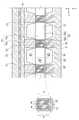
도 1은 본 발명의 제1 실시예에 따른 플라즈마 디스플레이 패널을 도시한 부분 분해사시도이고, 도 2는 도 1의 플라즈마 디스플레이 패널을 결합한 상태에서 Ⅱ-Ⅱ 선을 따라 잘라서 본 부분 단면도이다.1 is a partial exploded perspective view showing a plasma display panel according to a first embodiment of the present invention, Figure 2 is a partial cross-sectional view taken along the line II-II in the state in which the plasma display panel of Figure 1 combined.
도 1을 참조하면, 본 실시예에 따른 플라즈마 디스플레이 패널은 제1 기판(10)(이하 '배면기판'이라 함)과 제2 기판(20)(이하 '전면기판'이라 함)이 소정의 간격을 두고 대향 배치되고, 이 배면기판(10)과 전면기판(20)의 사이공간에는 다수의 방전셀(38)들이 격벽(16, 26)에 의해 구획된다.Referring to FIG. 1, in the plasma display panel according to the present exemplary embodiment, the first substrate 10 (hereinafter referred to as a "back substrate") and the second substrate 20 (hereinafter referred to as a "front substrate") are provided at predetermined intervals. The plurality of
방전셀(18) 내에는 자외선을 흡수하여 가시광을 방출하는 적색, 녹색 및 청색의 형광체층(19, 29)이 격벽면과 바닥면을 따라 형성되며, 플라즈마 방전을 일으킬 수 있도록 방전가스(일례로 제논(Xe), 네온(Ne) 등을 포함한 혼합가스)가 충전되어 있다.In the
전면기판(20)에 대향하는 배면기판(10)의 일면에는 일방향(도면의 y축 방향)을 따라 어드레스전극(12)들이 형성되고, 이들 어드레스전극(12)들을 덮으면서 배면기판(10)의 내면 전체에 유전층(14)이 형성된다. 어드레스전극(12)들은 이웃한 것끼리 서로 소정의 간격을 유지하면서 형성된다.
격벽(16, 26)은 배면기판(10)에 인접하여 전면기판(20)을 향해 돌출되는 제1 격벽층(16)(이하 '배면판 격벽'이라 한다)과, 전면기판(20)에 인접하여 배면기판 (10)을 향해 돌출되는 제2 격벽층(26)(이하 '전면판 격벽'이라 한다)을 포함한다.The
배면판 격벽(16)은 배면기판(10)에 형성되는 유전층(14) 위에 형성된다. 이러한 배면판 격벽(16)은 어드레스전극(12)과 나란한 방향(도면의 y축 방향)으로 배치되는 제1 격벽부재(16a)와, 이 격벽부재(16a)와 교차하는 방향(도면의 x축 방향)으로 형성되어 배면기판(10) 측에서 각 방전셀(18)을 독립적인 방전공간으로 구획하는 제2 격벽부재(16b)를 포함한다.The
그리고, 전면판 격벽(26)은 상기 제1 격벽부재(16a)와 대응하는 형상으로 이루어지는 제3 격벽부재(26a)와, 상기 제2 격벽부재(26a)와 대응하는 형상으로 이루어지는 제4 격벽부재(26b)를 포함한다. 즉, 제3 격벽부재(26a)와 제4 격벽부재(26b)는 이와 교차하는 방향(도면의 x축 방향)을 따라 형성되면서 배면기판(10) 측에 형성된 방전셀(18)과 대응하는 방전셀(28)을 전면기판(20) 측으로 형성한다.The
상기 배면판 격벽(16)에 의해 구획되는 방전셀(18)과 전면판 격벽(26)에 의해 구획되는 방전셀(28)이 실질적으로 하나의 방전셀(38)을 이루게 된다. 그리고, 본 실시예에서는 배면판 격벽(16)과 전면판 격벽(26)이 서로 교차하는 격벽부재들을 포함하여 형성되는 것을 설명하였으나, 본 발명은 이에 한정되는 것이 아니고 다양한 형상을 갖는 격벽이 적용될 수 있으며 이 또한 본 발명의 범위에 속한다.The
이러한 배면기판(10)측 방전셀(18)과 전면기판(20)측 방전셀(28)의 내에는 제1 형광체층(19)과 제2 형광체층(29)이 각각 형성된다. 제1 형광체층(19)은 배면판 격벽(16)을 이루는 격벽부재들(16a, 16b)의 측면과 그 사이에서 배면기판(10)과 인접한 바닥면에 형성되고, 제2 형광체층(29)은 전면판 격벽(26)을 이루는 격벽부 재들(26a, 26b)의 측면과 그 사이에서 전면기판(20)과 인접한 바닥면에 형성될 수 있다.The
제1 및 제2 형광체층(19, 29) 각각은 배면기판(10)측 방전셀 및 전면기판(20)측 방전셀 내부에서 진공자외선을 흡수하여 전면기판(20)쪽으로 향하는 가시광을 발생시킨다. 이 때, 제2 형광체층(29)은 이러한 가시광을 투과시키게 되므로, 진공자외선을 손실을 최소화하기 위하여 제2 형광체층(29)을 제1 형광체층(19)보다 더 얇게 형성할 수 있다.Each of the first and second phosphor layers 19 and 29 absorbs vacuum ultraviolet rays inside the discharge cell on the
배면판 격벽(16)에 의해 형성되는 방전셀(18)과 이에 대향하여 전면판 격벽(26)에 의하여 형성되는 방전셀(28)은 실질적으로 하나의 방전셀(38)이므로, 이 들의 내부 각각에 형성되는 제1 형광체층(19)과 제2 형광체층(29)은 기체방전으로 발생되는 진공자외선의 충돌에 의하여 같은 색의 가시광을 발광시키도록 동일한 색을 갖는 형광체층으로 형성되는 것이 바람직하다.Since the
본 실시예에서는 실질적으로 하나인 방전셀(38)의 양측으로 가시광을 방출시킬 수 있는 형광체층이 형성되므로 휘도를 향상시킬 수 있다.In this embodiment, since a phosphor layer capable of emitting visible light is formed on both sides of the
이 때, 전면기판(20) 측으로 형성되는 방전셀(28) 내에 형성되는 제2 형광체층(29)은 전면기판(10) 위에 유전층(미도시)을 형성하고 배면판 격벽(16)을 형성한다음 상기 유전층 위에 형광체를 도포함으로써 형성될 수 있고, 또한 선택적으로 도면에 도시된 바와 같이 유전층을 전면기판(20)에 형성하지 않고 전면기판(20) 위에 전면판 격벽(26)을 형성하고 형광체를 도포함으로써 형성될 수 있다.In this case, the
또는, 배면기판(10) 및 전면기판(20) 각각을 각 방전공간(38)의 형상에 상응 하도록 식각한 다음, 그 위에 형광체를 도포하여 제1 형광체층(19)과 제2 형광체층(29)을 각각 형성하는 것도 가능하다. 이 때, 배면판 격벽(16)과 배면기판(10)이 동일한 재료의 일체 구조로 이루어지게 되고, 전면판 격벽(26)과 전면기판(20)이 동일한 재료의 일체 구조로 이루어진다.Alternatively, each of the
그리고, 배면판 격벽(16)과 전면판 격벽(26)의 사이에는 각 방전셀(28)의 양측에서 어드레스전극(12)과 교차하는 방향을 따라 길게 이어지는 스트라이프 형태의 제1 전극(31)과 제2 전극(32)이 형성된다. 이러한 제1 전극(31)과 제2 전극(32)은 제1 격벽부재(16a)와 제3 격벽부재(26a) 사이를 가로지르면서 제2 격벽부재(16b)와 제4 격벽부재(26b) 사이에서 이와 나란하게 배치된다.In addition, between the back
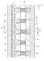
도 2를 참조하면, 본 실시예에서 제1 전극(31)은 길이방향에 수직한 평면으로 자른 단면이 기판(10, 20)면에 평행한 방향으로의 길이(w1)보다 기판(10, 20)면에 수직한 방향으로의 길이(h1)가 더 길게 형성될 수 있으며, 제2 전극(32)도 길이방향에 수직한 평면으로 자른 단면이 기판면에 평행한 방향으로의 길이(w2)보다 기판면에 수직한 방향으로의 길이(h2)가 더 길게 형성될 수 있다. 따라서 전극들(31, 32)간에 보다 쉽게 대향방전을 유도할 수 있으며, 이에 따라 높은 발광효율을 얻을 수 있다.Referring to FIG. 2, in this embodiment, the
본 실시예에서 제1 전극(31) 및 제2 전극(32)들은 실질적으로 표시에 기여하는 정도가 작은 방전셀(38)의 측방으로 형성되므로 전도성이 우수한 금속전극으로 이루어질 수 있다.In the present exemplary embodiment, since the
이 때, 제1 전극(31)은 어드레스전극(12)과 함께 어드레스 구간에서 스캔펄 스전압이 인가되면서 켜질 방전셀(38)을 선택하는 역할을 하고, 제2 전극(32)은 제1 전극(31)과 함께 유지구간의 방전에 관여하여 화면을 표시하는 역할을 한다. 그러나 각 전극들은 인가되는 신호전압에 따라 그 역할을 달리할 수 있으므로 본 발명은 이에 한정되지 않는다. At this time, the
그리고, 본 실시예에서 제1 전극(31) 및 제2 전극(32)들 각각은 외면이 유전층(34, 35)으로 둘러싸여 이루어진다. 이들은 TFCS(Thick Film Ceramic Sheet) 법으로 제작이 가능하다. 즉 제1 전극(31)과 제2 전극(32)을 포함하는 전극부를 따로 제작한 다음, 배면판 격벽(16)이 형성되어 있는 배면기판(10)에 결합하여 제작할 수 있다. 이러한 유전층(34, 35)은 각 전극들을 절연하는 동시에 방전에 의한 벽전하를 축적하는 역할을 한다.In the present embodiment, each of the first and
이러한 유전층(34, 35)의 표면에 MgO 보호막(36)이 형성될 수 있다. 이 때, MgO 보호막(36)은 방전셀(38) 내부의 방전공간에서 일어나는 플라즈마 방전에 노출되는 부분에 형성될 수 있다. 본 실시예에서 제1 전극(31) 및 제2 전극(32)은 양 기판(10)의 사이에서 실질적으로 표시에 기여하는 정도가 작은 부분에 위치하므로, 이들 제1 전극(31) 및 제2 전극(32)을 덮고 있는 유전층(34)에 도포되는 MgO 보호막(36)은 가시광 비투과성의 특성을 갖는 MgO 로 이루어질 수 있다. 이 가시광 비투과성 MgO는 가시광 투광성 MgO에 비하여 훨씬 높은 이차전자 방출 계수(secondary electron emission coefficient) 값을 가지며, 이에 따라 방전개시전압을 더욱 저감시킬 수 있다.The
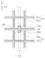
도 3은 본 발명의 제1 실시예에 따른 플라즈마 디스플레이 패널을 도시한 부 분 평면도이다.3 is a partial plan view showing a plasma display panel according to a first embodiment of the present invention.
도 3을 참조하면, 본 실시예에서 어드레스전극(12)은 각 방전셀(38)에 대응하여 형성되는 제1 부분(12a)과, 이러한 제1 부분(12a)의 사이에서 이들을 전기적으로 연결하는 제2 부분(12b)을 포함한다. 이러한 제1 부분(12a)의 평면 형상은 방전셀(38)의 형상에 따라 다양한 형태로 형성되는 것이 가능하며, 본 실시예에서는 일례로 사각형으로 되는 것을 예시하였다.Referring to FIG. 3, in the present embodiment, the
제1 부분(12a)과 제2 부분(12b)은 WA1 값이 WA2 보다 더 크게 형성될 수 있다. 여기서, WA1은 어드레스전극(12)의 제1 부분(12a)을 길이방향과 교차하는 방향(도면의 x축 방향)으로 측정한 폭이고, WA2는 제2 부분(12b)을 길이방향과 교차하는 방향(도면의 x축 방향)으로 측정한 폭이다.The
제1 부분(12a)은 각 방전셀(38)의 중심부에 대응하면서 제1 전극(31)과의 사이에서 어드레스방전이 일어나도록 유도하는 부분으로, 본 실시예에서는 이러한 제1 부분(12)의 폭을 넓힘으로써 제1 전극(31)과 제2 전극(32)의 측면 유전층에 많은 양의 벽전하가 쌓일 수 있도록 한다. 그리고, 어드레스방전에 기여하는 정도가 적은 제2 부분(12b)에서는 어드레스전극(12)의 폭을 줄임으로써 어드레스전극(12)에 흐르는 전류를 저감시킬 수 있다.The
제1 기판(10, 20)의 전면에서 볼 때, 어드레스전극의 제1 부분(12a)과 제1 전극(31)은 제1 간격(d1)을 두고 이격되고 상기 제1 부분(12a)과 제2 전극(32)은 제2 간격(d2)을 두고 이격된다. 이 때, 제1 부분(12)은 스캔전극으로 기능하는 제1 전극(31)과의 사이에서 어드레스방전을 일으키는 역할을 하므로, 제2 간격(d2)보다 제1 간격(d1)을 더 작게, 즉 제1 부분(12a)을 제1 전극(31)에 가깝게 형성함으로써 어드레스방전의 방전개시전압을 효과적으로 저감시킬 수 있다. 또는 선택적으로, 제1 간격(d1)과 제2 간격(d2)은 실질적으로 동일하게 형성될 수 있다.When viewed from the front of the
한편, 도 3에 도시된 바와 같이, 본 실시예에서 제1 전극(31)과 제2 전극(32)은 각 방전셀(38)에 한 쌍이 배치되는데 제1 전극(31)과 제2 전극(32)을 쌍으로 교호적으로 배치함에 있어서, 상기 어드레스전극(12)과 나란한 방향(도면의 y축 방향)으로 이웃하는 한 쌍의 방전셀(38)에 대하여 제1 전극(31)-제2 전극(32)과 제1 전극(31)-제2 전극(32)의 배열이 순차적으로 반복될 수 있다.Meanwhile, as shown in FIG. 3, in the present embodiment, a pair of the
이하에서는 본 발명의 제1 실시예에 대한 변형예들에 대하여 상세하게 설명한다. 제1 실시예의 변형예들은 제1 실시예와 기본적인 구성이 동일하므로, 제1 실시예와 동일한 구성요소는 동일한 참조부호를 사용한다.Hereinafter, modifications to the first embodiment of the present invention will be described in detail. Since the modifications of the first embodiment have the same basic configuration as the first embodiment, the same components as the first embodiment use the same reference numerals.
도 4는 본 발명의 제1 실시예에 대한 제1 변형예를 도시한 부분 단면도이다.4 is a partial sectional view showing a first modification to the first embodiment of the present invention.
도 4를 참조하면, 본 변형예에서는 배면판 격벽(41)과 전면판 격벽(42)이 어드레스전극(12)과 나란한 방향(도면의 y축 방향)으로 길게 이어지며 형성되는 스트라이프 형태이다. 제1 전극(31)과 제2 전극(32)은 이러한 배면판 격벽(41)과 전면판 격벽(42) 사이를 가로지르면서 이와 교차하는 방향(도면의 x축 방향)을 따라 형성된다.Referring to FIG. 4, in the present modified example, the
도 5는 본 발명의 제1 실시예에 대한 제2 변형예를 도시한 부분 평면도이다.5 is a partial plan view showing a second modification to the first embodiment of the present invention.
도 5를 참조하면, 본 변형예에서는 제1 전극(43)과 제2 전극(44)이 각 방전셀(38)에 한 쌍이 배치되고, 제1 전극(43)과 제2 전극(44)을 쌍으로 교호적으로 배 치함에 있어서 상기 어드레스전극(12)과 나란한 방향(도면의 y축 방향)으로 이웃하는 한 쌍의 방전셀(38)에 대하여 제1 전극(43)-제2 전극(44)과 제2 전극(44)-제2 전극(43)의 배열이 순차적으로 반복될 수 있다.Referring to FIG. 5, in the present modification, a pair of the
본 변형예에서는 각 방전셀(38)에 대응되는 제1 전극(43) 또는 제2 전극(44)들이 상기 이웃한 방전셀(38)에 대응되는 제1 전극(43) 또는 제2 전극(44)과 유전층(34) 내에서 이격되어 형성되어 이웃한 방전셀과 절연되고 크로스토크(cross talk)가 방지되므로, 이러한 구조를 갖는 것이 가능하다.In the present modification, the
도 6은 본 발명의 제1 실시예에 따른 제3 변형예를 도시한 부분 평면도이다.6 is a partial plan view showing a third modification according to the first embodiment of the present invention.
도 6을 참조하면, 본 변형예에서는 어드레스전극(12)과 나란한 방향(도면의 y축 방향)으로 이웃한 한 쌍의 방전셀에서 제2 전극(46)이 공유되어 형성된다. 따라서, 상기 한 쌍의 방전셀에서 제1 전극(45)-제2 전극(46)-제1 전극(45)의 배열을 갖는다. 이에 따라 유지전극으로 기능하는 제2 전극(46)은 상기 한 쌍의 방전셀의 유지 방전에 공통으로 관여하게 된다.Referring to FIG. 6, in the present modified example, the
도 7은 본 발명의 제1 실시예에 따른 제4 변형예를 도시한 부분 단면도이다.7 is a partial sectional view showing a fourth modification according to the first embodiment of the present invention.
도 7을 참조하면, 본 변형예에서는 전면기판(20)에 인접한 부분에서 흑색층(47)이 형성된다. 흑색층(47)은 전면기판(20) 표면에 형성할 수 있으며, 또는 전면기판(20) 위에 유전층(미도시)이 형성되는 경우에는 이러한 유전층 위에 흑색층(47)을 형성할 수 있다. 따라서, 흑색층(47)은 전면기판(20)과 전면판 격벽(26) 사이에 형성된다.Referring to FIG. 7, a
전면기판(20) 측으로 흑색층(47)을 형성함으로써 외부의 광이 반사되는 것을 방지할 수 있고, 이에 따라 명실 콘트라스트를 향상할 수 있다. 이 때, 흑색층(47)을 제1 전극(31)과 제2 전극(32)이 형성되는 부분에 대응하여 형성함으로써, 방전에 의해 발생된 가시광을 차단하지 않으면서 명실 콘트라스트를 향상시킬 수 있다.By forming the
도 8은 본 발명의 제1 실시예에 따른 제5 변형예를 도시한 부분 단면도이다.8 is a partial sectional view showing a fifth modification according to the first embodiment of the present invention.
도 8을 참조하면, 본 변형예에서는 전면판 격벽(48) 및 배면판 격벽(16)을 이루는 격벽부재 중 적어도 어느 하나를 착색함으로써 명실 콘트라스트를 향상한다. 일례로, 전면판 격벽(48)의 제2 격벽부재(48b)가 흑색 안료 등으로 착색될 수 있는데, 제2 격벽부재(48b) 만을 착색함으로써 방전에 의해 발생되는 가시광을 차단하지 않으면서 외광의 반사를 방지할 수 있다. 흑색 안료는 일례로 FeO, RuO2, TiO, Ti3O5, Ni2O3, CrO2, MnO2, Mn2O3, Mo2O3, Fe3O4 중 어느 하나 또는 이들의 조합으로 이루어질 수 있다.Referring to FIG. 8, in this modification, at least one of the partition members constituting the front
이하에서는 본 발명의 제2 실시예에 따른 플라즈마 디스플레이 패널에 대하여 상세하게 설명한다. 본 발명의 제2 실시예는 제1 실시예와 기본적인 구성이 동일하고, 전극의 형상과 배치, 격벽 및 방전셀의 형상이 서로 다른 실시예이다. 제2 실시예에서 제1 실시예와 동일한 구성요소는 동일한 참조부호를 사용하고, 동일한 구성은 상세 설명을 생략하고 서로 다른 부분에 대해서 설명한다.Hereinafter, a plasma display panel according to a second exemplary embodiment of the present invention will be described in detail. The second embodiment of the present invention is an embodiment in which the basic configuration is the same as that of the first embodiment, and the shapes and arrangements of the electrodes, the partitions, and the discharge cells are different from each other. In the second embodiment, the same components as those in the first embodiment use the same reference numerals, and the same components will not be described in detail, and different parts will be described.
도 9는 본 발명의 제2 실시예에 따른 플라즈마 디스플레이 패널을 도시한 부분 분해사시도이고, 도 10은 도 9의 플라즈마 디스플레이 패널을 결합한 상태에서 Ⅹ-Ⅹ 선을 따라 잘라서 본 부분 단면도이다.FIG. 9 is a partially exploded perspective view illustrating a plasma display panel according to a second exemplary embodiment of the present invention, and FIG. 10 is a partial cross-sectional view taken along a line VII-V in a state in which the plasma display panel of FIG. 9 is coupled.
도 9 및 도 10을 참조하면, 본 실시예에 따른 배면판 격벽(116)은 제2 격벽부재(116b)들 사이에서 배면기판(10) 측으로 형성되는 방전셀(118)을 두 방전공간(118a, 118b)으로 구획하는 제5 격벽부재(116c)를 포함한다.9 and 10, the
즉, 본 실시예에서 배면판 격벽(116)은 어드레스전극(112)과 나란한 방향(도면의 y축 방향)으로 형성되는 제1 격벽부재(116a)와, 이 제1 격벽부재(116a)와 교차하는 방향(도면의 x축 방향)으로 형성되며 배면기판(10) 측에 형성되는 각 방전셀(118)을 독립적인 공간으로 구획하는 제2 격벽부재(116b)와, 제2 격벽부재(116b) 사이에서 이와 나란한 방향(도면의 x축 방향)으로 형성되어 상기 방전셀(118)을 두 방전공간(118a, 118b)으로 구획하는 제5 격벽부재(116c)를 포함한다.That is, in this embodiment, the back
전면판 격벽(126)은 제1 격벽부재(116a)와 대응하는 형상으로 이루어지는 제3 격벽부재(126a)와, 제2 격벽부재(126a)와 대응하는 형상으로 이루어지는 제4 격벽부재(126b)를 포함하여 상기 방전셀(118)에 대응하도록 전면기판(20) 측에 방전셀(128)을 형성한다.The
상기 배면판 격벽(116)에 의해 구획되는 방전셀(118)과 전면판 격벽(126)에 의해 구획되는 방전셀(128)이 실질적으로 하나의 방전셀(138)을 이루게 된다.The
그리고, 전면판 격벽(116)과 배면판 격벽(126) 사이에는 각 방전셀(138)의 양측에 어드레스전극(112)과 교차하는 방향으로 이어지는 한 쌍의 제1 전극(131)이 나란히 형성된다. 이러한 제1 전극(131)들은 제2 격벽부재(16b)와 제4 격벽부재(26b) 사이에서 이들 각각에 하나씩 대응되어 제2 격벽부재(16b) 위를 지나도록 배치되므로, 어드레스전극(112)과 나란한 방향(도면의 y축 방향)으로 이웃하는 방전 셀(138)들을 구분하는 기준이 될 수 있다.In addition, a pair of
이러한 한 쌍의 제1 전극(131)들 사이에서 제1 전극(131)들과 나란한 방향(도면의 x축 방향)을 따라 길게 이어지면서 제2 전극(132)이 형성되어, 각 방전셀(138)에서 제1 전극(131)과 제2 전극(132) 사이에 공간을 두고 서로 대향하면서 형성된다. 제2 전극(132)은 각 방전셀(138)을 관통하면서 형성된다.A
또한, 본 실시에에서는 제1 전극(131)과 제2 전극(132)간에 일어나는 유지방전의 방전 갭이 줄어들어 방전개시전압을 더욱 저감시킬 수 있다. 즉, 방전셀(138)을 가로지르는 제2 전극(132)과 그 양쪽으로 배치된 한 쌍의 제1 전극(131)들 사이에서 방전을 일으키는 것이므로, 방전유지에 관여하는 전극들이 방전셀 가장자리에 각각 인접하는 경우보다 방전을 일으키는 두 전극 사이의 방전갭이 절반 가까이 줄어들게 되고, 따라서 낮은 방전개시전압으로도 구동이 가능하다.In addition, in the present embodiment, the discharge gap of the sustain discharge occurring between the
이 때, 제1 전극(131)은 어드레스전극(112)과 함께 어드레스 구간에서 스캔펄스전압이 인가되면서 켜질 방전셀(138)을 선택하는 역할을 하고, 제2 전극(132)은 제1 전극(131)과 함께 유지구간의 방전에 관여하여 화면을 표시하는 역할을 한다. 그러나 각 전극들은 인가되는 신호전압에 따라 그 역할을 달리할 수 있으므로 본 발명은 이에 한정되지 않는다. In this case, the
본 실시예에서 제1 전극(131)들은 실질적으로 표시에 기여하는 정도가 작은 방전셀(138)의 측방으로 형성되므로 전도성이 우수한 금속전극으로 이루어질 수 있다. 제2 전극(132)들은 전도성이 우수한 금속전극으로 이루어질 수 있고, 불투명한 금속전극을 형성함으로써 명실 콘트라스트를 향상시킬 수 있다.In the present exemplary embodiment, since the
그리고, 본 실시예에서 제1 전극(31) 및 제2 전극(32)들 각각은 외면이 유전층(34, 35)으로 둘러싸여 이루어진다. 이러한 유전층(34, 35)의 표면에 MgO 보호막(36)이 형성될 수 있다. 이 때, MgO 보호박(36)은 가시광 비투과성의 특성을 갖는 MgO 로 이루어질 수 있다. 이 가시광 비투과성 MgO는 높은 이차전자 방출 계수(secondary electron emission coefficient) 값을 가지며, 이에 따라 방전개시전압을 더욱 저감시킬 수 있다.In the present embodiment, each of the first and
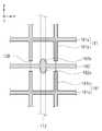
도 11은 본 발명의 제2 실시예에 따른 플라즈마 디스플레이 패널을 도시한 부분 평면도이고, 도 12는 본 발명의 제2 실시예에 따른 플라즈마 디스플레이 패널에서 하나의 방전셀에 대응하는 전극의 구조를 도시한 부분 평면도이다.FIG. 11 is a partial plan view of a plasma display panel according to a second embodiment of the present invention, and FIG. 12 illustrates a structure of an electrode corresponding to one discharge cell in the plasma display panel according to the second embodiment of the present invention. One part plan view.
본 실시예에서 배면기판(10)에서 일방향(도면의 y축 방향)을 따라 형성되는 어드레스전극(112)은 균일한 선폭을 가지며 형성된다.In the present exemplary embodiment, the
그리고, 도 11을 참조하면, 본 실시예에서 제1 전극(131)은 어드레스전극(112)과 교차하는 방향(도면의 x축 방향)을 따라 위치하는 제1 부분(131a)과, 이러한 제1 부분(131a)으로부터 제2 전극(132)을 향해 돌출되는 제2 부분(131b)을 포함한다. 이 때, 제1 부분(131a)은 제2 격벽부재(116b)와 제4 격벽부재(126b) 사이에서 제2 격벽부재(116b) 위에 배치되고 제2 부분(131b)은 제1 격벽부재(116a)와 제3 격벽부재(116b) 사이에서 제1 격벽부재(116a) 위에 배치된다.Referring to FIG. 11, in the present embodiment, the
본 실시예에서 제1 부분(131a)은 어드레스전극(112)과 나란한 방향(도면의 y축 방향)으로 이웃한 쌍의 방전셀에 공유되고 제2 부분(131b)은 어드레스전극(112)과 교차하는 방향(도면의 x축 방향)으로 이웃하는 한 쌍의 방전셀에 공유된다. 이 때, 제2 부분(131b)은 균일한 선폭을 가지면서 형성된다.In the present embodiment, the
한 쌍의 제1 전극(131)들의 제2 부분(131b) 각각은 방전셀(138)의 양측으로 형성되어 각 방전셀(138)에서 서로 마주보며 형성될 수 있다. 이러한 구조를 갖는 제1 전극(131)의 제1 부분(131a)과 제2 부분(131b)을 가짐으로써 각각의 제1 전극(131)은 각 방전셀(18)의 세 측면을 둘러싸면서 형성될 수 있다. 방전셀(138)의 방전공간 각각은 세 측면에 제1 전극(131)이 배치되고 다른 일 측면에 제2 전극(132)이 배치됨으로써, 제1 전극(131)과 제2 전극(132) 사이에 발생되는 유지방전의 방전 공간을 보다 효율적으로 사용할 수 있다.Each of the
도 12를 참조하면, 이러한 구조를 가짐으로써 제1 전극(131)과 제2 전극(132) 사이의 거리를 어드레스전극(112)과 나란한 방향(도면의 y축 방향)을 따라 측정한 길이는, 방전셀(138)의 가장자리에서보다 방전셀(138)의 중심부에서 더 크게 형성된다. 즉, 제1 전극(131)과 제2 전극(132)은 방전셀(138) 가장자리에서 숏 갭(short gap)(G1)을 갖고 방전셀(138) 중심부에서 롱 갭(long gap)(G2)을 갖는다.Referring to FIG. 12, having such a structure, the length of the distance between the
따라서, 제1 전극(131)과 제2 전극(132) 사이에서 일어나는 유지방전은, 방전셀(138) 가장자리의 숏 갭(G1)에서 개시되어 방전셀(138) 중심부의 롱 갭(G2)으로 확산된다. 유지방전이 숏 갭(G1)에서 개시되어 방전개시전압을 낮추면서 주방전은 상대적으로 긴 방전 길이를 갖는 롱 갭(G2)에서 유지되어 방전효율을 향상시킬 수 있다.Therefore, the sustain discharge occurring between the
또한, 본 실시에에서는 방전개시전압을 효과적으로 저감시킬 수 있으므로 Xe 가스의 분압을 높일 수 있고 이에 따라 방전효율을 향상시킬 수 있다.In addition, in this embodiment, since the discharge start voltage can be effectively reduced, the partial pressure of the Xe gas can be increased, thereby improving the discharge efficiency.
이하에서는 본 발명의 제3 실시예 및 제5 실시예에 대하여 상세하게 설명한다. 제3 실시예 및 제5 실시예는 제2 실시예와 기본적인 구성이 동일하므로, 제2 실시예와 동일한 구성요소는 동일한 참조부호를 사용한다.Hereinafter, a third embodiment and a fifth embodiment of the present invention will be described in detail. Since the third embodiment and the fifth embodiment have the same basic configuration as the second embodiment, the same components as the second embodiment use the same reference numerals.
도 13은 본 발명의 제3 실시예에 따른 플라즈마 디스플레이 패널에서 하나의 방전셀에 대응하는 전극의 구조를 도시한 부분 평면도이다.FIG. 13 is a partial plan view illustrating a structure of an electrode corresponding to one discharge cell in the plasma display panel according to the third embodiment of the present invention.
제1 전극들(141)은 각 방전셀(138)의 양측에서 어드레스전극(112)과 교차하는 방향(도면의 y축 방향)으로 이어지면서 형성되고, 이러한 제1 전극들(141) 사이로 방전셀(138)을 관통하면서 제2 전극(142)이 형성된다.The
이 때, 제1 전극들(141) 각각은 어드레스전극(112)과 교차하는 방향(도면의 x축 방향)을 따라 형성되는 제1 부분(141a)과, 어드레스전극(112)과 나란한 방향(도면의 y축 방향)을 따라 방전셀(138)의 양측으로 형성되서 한 쌍이 서로 마주보며 형성되는 제2 부분(141b)을 포함한다. 이에 따라 각각의 제1 전극(141)은 각 방전셀(138)의 세 측면을 둘러싸면서 형성되어 방전 공간을 보다 효율적으로 사용할 수 있다.In this case, each of the
도 13을 참조하면, 본 실시예에서는 제1 전극(141)의 제2 부분(141b)은 방전셀(138)의 중심으로부터 어드레스전극(112)과 나란한 방향으로 위치하는 방전셀(138)의 단부를 향하면서 선폭이 점진적으로 커지게 되고, 제 2전극(132)에 대향하는 대향면이 곡면으로 이루어지게 된다. 제1 전극(131)이 이러한 곡면을 가짐으로써 방전의 확산을 보다 용이하게 할 수 있다.Referring to FIG. 13, in the present embodiment, the
본 실시예에서는 제1 전극(131)과 제2 전극(132) 사이에서 일어나는 유지 방 전이, 방전셀(138) 가장자리에서 숏 갭에서 개시되어 중심부의 롱 갭으로 확산됨으로써 방전개시전압을 낮추면서 효율을 향상시킬 수 있다.In this embodiment, the sustain discharge occurs between the
도 14는 본 발명의 제4 실시예에 따른 플라즈마 디스플레이 패널에서 하나의 방전셀에 대응하는 전극의 구조를 도시한 부분 평면도이다.14 is a partial plan view showing a structure of an electrode corresponding to one discharge cell in the plasma display panel according to the fourth embodiment of the present invention.
제1 전극들(151)은 각 방전셀(138)의 양측에서 어드레스전극(112)과 교차하는 방향(도면의 y축 방향)으로 길게 이어지면서 형성되고, 이러한 제1 전극들(151) 사이로 방전셀(138)을 관통하면서 제2 전극(152)이 형성된다. 제1 전극들(151)과 제2 전극(152)이 서로 대향하면서 형성됨으로써 유지방전이 대향방전으로 유도될 수 있어 방전개시전압을 저감시킬 수 있다.The
이 때, 제1 전극들(151) 각각은 어드레스전극(112)과 교차하는 방향(도면의 x축 방향)을 따라 형성되는 제1 부분(151a)과, 어드레스전극(112)과 나란한 방향(도면의 y축 방향)을 따라 방전셀(138)의 양측으로 형성되서 한 쌍이 서로 마주보며 형성되는 제2 부분(151b)을 포함한다. 이에 따라 각각의 제1 전극(151)은 각 방전셀(138)의 세 측면을 둘러싸면서 형성되어 방전 공간을 보다 효율적으로 사용할 수 있다.In this case, each of the
도 14를 참조하면, 본 실시예에서는 제2 전극(152)에는 제1 전극(151)의 제1 부분(151a) 각각을 향해 돌출되는 돌출부(152a)를 포함한다. 제2 전극(152)의 돌출부(152a)는 각 방전셀(138)에서 한 쌍이 마주보며 형성되는 제2 부분(151b) 사이에서 형성되어 각 방전셀(138)의 중심부에 대응되어 형성되고, 이러한 각 돌출부(152a)의 평면 형상은 사각형으로 이루어진다. 돌출부(152a)의 평면 형상이 사각형 으로 이루어짐으로써, 돌출부(152a)가 제1 전극(151)과 제2 전극(152) 사이에서 넓게 형성되면서 제1 전극(151)과 제2 전극(152) 사이에서 숏 갭을 이루는 부분을 넓게 형성할 수 있다.Referring to FIG. 14, in the present embodiment, the
제2 전극(152)의 이러한 돌출부 부분과 방전셀(138)의 가장자리 부분의 숏 갭에서 유지방전이 개시되어 방전개시전압을 낮출 수 있고, 이에 따라 Xe 가스의 분압을 높일 수 있어 효율을 향상시킬 수 있다.The sustain discharge is initiated at the short gap between the protruding portion of the
도 15는 본 발명의 제5 실시예에 따른 플라즈마 디스플레이 패널에서 하나의 방전셀에 대응하는 전극 구조를 도시한 부분 평면도이다.15 is a partial plan view illustrating an electrode structure corresponding to one discharge cell in the plasma display panel according to the fifth embodiment of the present invention.
도 15를 참조하면, 본 실시예에서는 제2 전극(162)에는 제1 전극(161)의 제1 부분(161a) 각각을 향해 돌출되는 돌출부(162a)를 포함한다. 제2 전극(162)의 돌출부(162a)는 각 방전셀(138)에서 한 쌍이 마주보며 형성되는 제2 부분(161b) 사이에서 형성되어 각 방전셀(138)의 중심부에 대응되어 형성되고, 이러한 각 돌출부(162a)의 평면 형상은 반원 형상 또는 타원형 형상으로 이루어진다.Referring to FIG. 15, in the present embodiment, the
제2 전극(162)의 이러한 돌출부(162a)는 숏 갭을 이루는 제1 전극(161)과 제2 전극(162)의 부분을 증가시킴으로써 방전개시전압을 낮출 수 있고, 이에 따라 Xe 가스의 분압을 높일 수 있어 효율을 향상시킬 수 있다.The
이상을 통해 본 발명의 바람직한 실시예에 대하여 설명하였지만, 본 발명은 이에 한정되는 것이 아니고 특허청구범위와 발명의 상세한 설명 및 첨부한 도면의 범위 안에서 여러 가지로 변형 또는 변경하여 실시하는 것이 가능하고 이 또한 본 발명의 범위에 속하는 것은 당연하다.Although the preferred embodiments of the present invention have been described above, the present invention is not limited thereto, and various modifications or changes can be made within the scope of the claims and the detailed description of the invention and the accompanying drawings. It goes without saying that it belongs to the scope of the present invention.
이상 설명한 바와 같이 본 발명에 따른 플라즈마 디스플레이 패널에 의하면, 어드레스방전과 유지방전을 대향방전으로 유도함으로써 방전개시전압을 저감시킬 수 있다. 또한, 어드레스방전 또는 유지방전에 관여하는 전극에 돌출부를 형성하여 숏 갭 방전과 롱 갭 방전을 이용할 수 있어 방전개시전압을 더욱 저감시키면서 방전효율을 향상시킬 수 있다.As described above, according to the plasma display panel according to the present invention, the discharge start voltage can be reduced by inducing the address discharge and the sustain discharge to the opposite discharge. In addition, short gap discharge and long gap discharge can be used by forming protrusions on electrodes involved in address discharge or sustain discharge, thereby improving discharge efficiency while further reducing discharge start voltage.
또한 전면기판에 전극을 형성하지 않아도 되므로 PDP 제작원가가 절감될 뿐만 아니라 가시광 투과율도 높일 수 있다. 아울러 가시광 투과성 MgO에 비하여 훨씬 높은 이차전자 방출계수값을 갖는 가시광 비투과성 MgO를 보호막으로 이용함으로써 방전개시전압을 더욱 낮출 수 있으며, 전면기판에도 형광체를 형성함으로써, 진공자외선의 손실을 최소화하여 발광효율을 높일 수 있다.In addition, since the electrode is not formed on the front substrate, the manufacturing cost of the PDP can be reduced and the visible light transmittance can be increased. In addition, by using a visible light impermeable MgO having a much higher secondary electron emission coefficient as a protective film than a visible light transmissive MgO, the discharge initiation voltage can be further lowered, and a fluorescent material is formed on the front substrate to minimize the loss of vacuum ultraviolet rays and thus the luminous efficiency. Can increase.
Claims (37)
Translated fromKoreanPriority Applications (4)
| Application Number | Priority Date | Filing Date | Title |
|---|---|---|---|
| KR1020040096208AKR100658716B1 (en) | 2004-11-23 | 2004-11-23 | Plasma display panel |
| JP2005224540AJP2006147530A (en) | 2004-11-23 | 2005-08-02 | Plasma display panel |
| US11/281,714US20060108925A1 (en) | 2004-11-23 | 2005-11-18 | Plasma display panel |
| CNB2005101242013ACN100533641C (en) | 2004-11-23 | 2005-11-21 | plasma display panel |
Applications Claiming Priority (1)
| Application Number | Priority Date | Filing Date | Title |
|---|---|---|---|
| KR1020040096208AKR100658716B1 (en) | 2004-11-23 | 2004-11-23 | Plasma display panel |
Publications (2)
| Publication Number | Publication Date |
|---|---|
| KR20060057139A KR20060057139A (en) | 2006-05-26 |
| KR100658716B1true KR100658716B1 (en) | 2006-12-15 |
Family
ID=36460320
Family Applications (1)
| Application Number | Title | Priority Date | Filing Date |
|---|---|---|---|
| KR1020040096208AExpired - Fee RelatedKR100658716B1 (en) | 2004-11-23 | 2004-11-23 | Plasma display panel |
Country Status (4)
| Country | Link |
|---|---|
| US (1) | US20060108925A1 (en) |
| JP (1) | JP2006147530A (en) |
| KR (1) | KR100658716B1 (en) |
| CN (1) | CN100533641C (en) |
Families Citing this family (2)
| Publication number | Priority date | Publication date | Assignee | Title |
|---|---|---|---|---|
| KR100542189B1 (en)* | 2003-09-04 | 2006-01-10 | 삼성에스디아이 주식회사 | Plasma Display Panel with Improved Address Electrode Structure |
| KR100684727B1 (en)* | 2005-06-27 | 2007-02-21 | 삼성에스디아이 주식회사 | Plasma display panel |
Citations (4)
| Publication number | Priority date | Publication date | Assignee | Title |
|---|---|---|---|---|
| KR19980061397A (en)* | 1996-12-31 | 1998-10-07 | 구자홍 | AC opposed discharge plasma display panel |
| KR20010047131A (en)* | 1999-11-18 | 2001-06-15 | 구자홍 | Radio Frequency Plasma Display Panel Driving |
| KR20060001547A (en)* | 2004-06-30 | 2006-01-06 | 삼성에스디아이 주식회사 | Plasma display panel |
| KR20060001544A (en)* | 2004-06-30 | 2006-01-06 | 삼성에스디아이 주식회사 | Plasma display panel |
Family Cites Families (4)
| Publication number | Priority date | Publication date | Assignee | Title |
|---|---|---|---|---|
| CA2149289A1 (en)* | 1994-07-07 | 1996-01-08 | Yoshifumi Amano | Discharge display apparatus |
| JP2001035383A (en)* | 1999-07-15 | 2001-02-09 | Sony Corp | Flat display device and manufacture thereof |
| JP3594857B2 (en)* | 1999-11-26 | 2004-12-02 | パイオニア株式会社 | Plasma display panel |
| JP2003257321A (en)* | 2002-03-06 | 2003-09-12 | Pioneer Electronic Corp | Plasma display panel |
- 2004
- 2004-11-23KRKR1020040096208Apatent/KR100658716B1/ennot_activeExpired - Fee Related
- 2005
- 2005-08-02JPJP2005224540Apatent/JP2006147530A/enactivePending
- 2005-11-18USUS11/281,714patent/US20060108925A1/ennot_activeAbandoned
- 2005-11-21CNCNB2005101242013Apatent/CN100533641C/ennot_activeExpired - Fee Related
Patent Citations (4)
| Publication number | Priority date | Publication date | Assignee | Title |
|---|---|---|---|---|
| KR19980061397A (en)* | 1996-12-31 | 1998-10-07 | 구자홍 | AC opposed discharge plasma display panel |
| KR20010047131A (en)* | 1999-11-18 | 2001-06-15 | 구자홍 | Radio Frequency Plasma Display Panel Driving |
| KR20060001547A (en)* | 2004-06-30 | 2006-01-06 | 삼성에스디아이 주식회사 | Plasma display panel |
| KR20060001544A (en)* | 2004-06-30 | 2006-01-06 | 삼성에스디아이 주식회사 | Plasma display panel |
Also Published As
| Publication number | Publication date |
|---|---|
| JP2006147530A (en) | 2006-06-08 |
| KR20060057139A (en) | 2006-05-26 |
| US20060108925A1 (en) | 2006-05-25 |
| CN1783398A (en) | 2006-06-07 |
| CN100533641C (en) | 2009-08-26 |
Similar Documents
| Publication | Publication Date | Title |
|---|---|---|
| EP1684322B1 (en) | Plasma display panel | |
| JP2006202763A (en) | Plasma display panel and driving method of plasma display panel | |
| KR100658716B1 (en) | Plasma display panel | |
| KR100637466B1 (en) | Plasma display panel | |
| KR100578936B1 (en) | Plasma Display Panel and Driving Method thereof | |
| KR100578983B1 (en) | Plasma display panel | |
| KR100637465B1 (en) | Plasma display panel | |
| KR100599627B1 (en) | Plasma display panel | |
| KR100658750B1 (en) | Plasma display panel | |
| JP2004311274A (en) | Plasma display panel | |
| KR100612394B1 (en) | Plasma display panel | |
| KR100649229B1 (en) | Plasma display panel | |
| KR100649228B1 (en) | Plasma display panel | |
| KR100649232B1 (en) | Plasma display panel | |
| KR100669465B1 (en) | Plasma Display Panel and Driving Method thereof | |
| KR100649231B1 (en) | Plasma display panel | |
| KR100612354B1 (en) | Plasma display panel | |
| KR100612288B1 (en) | Plasma Display Panel and Driving Method thereof | |
| KR100599629B1 (en) | Plasma display panel | |
| KR100658745B1 (en) | Plasma Display Panel and Driving Method thereof | |
| KR100667940B1 (en) | Plasma Display Panel and Driving Method thereof | |
| KR100590095B1 (en) | Plasma display panel | |
| KR100658720B1 (en) | Plasma display panel | |
| KR20060102664A (en) | Plasma display panel | |
| KR20060088219A (en) | Plasma Display Panel and Driving Method thereof |
Legal Events
| Date | Code | Title | Description |
|---|---|---|---|
| A201 | Request for examination | ||
| PA0109 | Patent application | St.27 status event code:A-0-1-A10-A12-nap-PA0109 | |
| PA0201 | Request for examination | St.27 status event code:A-1-2-D10-D11-exm-PA0201 | |
| D13-X000 | Search requested | St.27 status event code:A-1-2-D10-D13-srh-X000 | |
| D14-X000 | Search report completed | St.27 status event code:A-1-2-D10-D14-srh-X000 | |
| E902 | Notification of reason for refusal | ||
| PE0902 | Notice of grounds for rejection | St.27 status event code:A-1-2-D10-D21-exm-PE0902 | |
| PG1501 | Laying open of application | St.27 status event code:A-1-1-Q10-Q12-nap-PG1501 | |
| P11-X000 | Amendment of application requested | St.27 status event code:A-2-2-P10-P11-nap-X000 | |
| P13-X000 | Application amended | St.27 status event code:A-2-2-P10-P13-nap-X000 | |
| E701 | Decision to grant or registration of patent right | ||
| PE0701 | Decision of registration | St.27 status event code:A-1-2-D10-D22-exm-PE0701 | |
| GRNT | Written decision to grant | ||
| PR0701 | Registration of establishment | St.27 status event code:A-2-4-F10-F11-exm-PR0701 | |
| PR1002 | Payment of registration fee | St.27 status event code:A-2-2-U10-U11-oth-PR1002 Fee payment year number:1 | |
| PG1601 | Publication of registration | St.27 status event code:A-4-4-Q10-Q13-nap-PG1601 | |
| R17-X000 | Change to representative recorded | St.27 status event code:A-5-5-R10-R17-oth-X000 | |
| R18-X000 | Changes to party contact information recorded | St.27 status event code:A-5-5-R10-R18-oth-X000 | |
| LAPS | Lapse due to unpaid annual fee | ||
| PC1903 | Unpaid annual fee | St.27 status event code:A-4-4-U10-U13-oth-PC1903 Not in force date:20091212 Payment event data comment text:Termination Category : DEFAULT_OF_REGISTRATION_FEE | |
| R18-X000 | Changes to party contact information recorded | St.27 status event code:A-5-5-R10-R18-oth-X000 | |
| PC1903 | Unpaid annual fee | St.27 status event code:N-4-6-H10-H13-oth-PC1903 Ip right cessation event data comment text:Termination Category : DEFAULT_OF_REGISTRATION_FEE Not in force date:20091212 | |
| P22-X000 | Classification modified | St.27 status event code:A-4-4-P10-P22-nap-X000 | |
| R18-X000 | Changes to party contact information recorded | St.27 status event code:A-5-5-R10-R18-oth-X000 | |
| R18-X000 | Changes to party contact information recorded | St.27 status event code:A-5-5-R10-R18-oth-X000 |