KR100656490B1 - Full color organic light emitting display device and manufacturing method thereof - Google Patents
Full color organic light emitting display device and manufacturing method thereofDownload PDFInfo
- Publication number
- KR100656490B1 KR100656490B1KR1020010073822AKR20010073822AKR100656490B1KR 100656490 B1KR100656490 B1KR 100656490B1KR 1020010073822 AKR1020010073822 AKR 1020010073822AKR 20010073822 AKR20010073822 AKR 20010073822AKR 100656490 B1KR100656490 B1KR 100656490B1
- Authority
- KR
- South Korea
- Prior art keywords
- layer
- delete delete
- thin film
- insulating film
- light emitting
- Prior art date
- Legal status (The legal status is an assumption and is not a legal conclusion. Google has not performed a legal analysis and makes no representation as to the accuracy of the status listed.)
- Expired - Lifetime
Links
Images


Classifications
- H—ELECTRICITY
- H10—SEMICONDUCTOR DEVICES; ELECTRIC SOLID-STATE DEVICES NOT OTHERWISE PROVIDED FOR
- H10K—ORGANIC ELECTRIC SOLID-STATE DEVICES
- H10K59/00—Integrated devices, or assemblies of multiple devices, comprising at least one organic light-emitting element covered by group H10K50/00
- H10K59/10—OLED displays
- H10K59/12—Active-matrix OLED [AMOLED] displays
- H10K59/122—Pixel-defining structures or layers, e.g. banks
- H—ELECTRICITY
- H05—ELECTRIC TECHNIQUES NOT OTHERWISE PROVIDED FOR
- H05B—ELECTRIC HEATING; ELECTRIC LIGHT SOURCES NOT OTHERWISE PROVIDED FOR; CIRCUIT ARRANGEMENTS FOR ELECTRIC LIGHT SOURCES, IN GENERAL
- H05B33/00—Electroluminescent light sources
- H05B33/10—Apparatus or processes specially adapted to the manufacture of electroluminescent light sources
- H—ELECTRICITY
- H10—SEMICONDUCTOR DEVICES; ELECTRIC SOLID-STATE DEVICES NOT OTHERWISE PROVIDED FOR
- H10K—ORGANIC ELECTRIC SOLID-STATE DEVICES
- H10K71/00—Manufacture or treatment specially adapted for the organic devices covered by this subclass
- H10K71/10—Deposition of organic active material
- H10K71/18—Deposition of organic active material using non-liquid printing techniques, e.g. thermal transfer printing from a donor sheet
- H—ELECTRICITY
- H10—SEMICONDUCTOR DEVICES; ELECTRIC SOLID-STATE DEVICES NOT OTHERWISE PROVIDED FOR
- H10K—ORGANIC ELECTRIC SOLID-STATE DEVICES
- H10K2102/00—Constructional details relating to the organic devices covered by this subclass
- H10K2102/301—Details of OLEDs
- H10K2102/351—Thickness
- H—ELECTRICITY
- H10—SEMICONDUCTOR DEVICES; ELECTRIC SOLID-STATE DEVICES NOT OTHERWISE PROVIDED FOR
- H10K—ORGANIC ELECTRIC SOLID-STATE DEVICES
- H10K59/00—Integrated devices, or assemblies of multiple devices, comprising at least one organic light-emitting element covered by group H10K50/00
- H10K59/10—OLED displays
- H10K59/12—Active-matrix OLED [AMOLED] displays
- H—ELECTRICITY
- H10—SEMICONDUCTOR DEVICES; ELECTRIC SOLID-STATE DEVICES NOT OTHERWISE PROVIDED FOR
- H10K—ORGANIC ELECTRIC SOLID-STATE DEVICES
- H10K59/00—Integrated devices, or assemblies of multiple devices, comprising at least one organic light-emitting element covered by group H10K50/00
- H10K59/30—Devices specially adapted for multicolour light emission
- H10K59/35—Devices specially adapted for multicolour light emission comprising red-green-blue [RGB] subpixels
- H—ELECTRICITY
- H10—SEMICONDUCTOR DEVICES; ELECTRIC SOLID-STATE DEVICES NOT OTHERWISE PROVIDED FOR
- H10K—ORGANIC ELECTRIC SOLID-STATE DEVICES
- H10K71/00—Manufacture or treatment specially adapted for the organic devices covered by this subclass
- Y—GENERAL TAGGING OF NEW TECHNOLOGICAL DEVELOPMENTS; GENERAL TAGGING OF CROSS-SECTIONAL TECHNOLOGIES SPANNING OVER SEVERAL SECTIONS OF THE IPC; TECHNICAL SUBJECTS COVERED BY FORMER USPC CROSS-REFERENCE ART COLLECTIONS [XRACs] AND DIGESTS
- Y10—TECHNICAL SUBJECTS COVERED BY FORMER USPC
- Y10T—TECHNICAL SUBJECTS COVERED BY FORMER US CLASSIFICATION
- Y10T428/00—Stock material or miscellaneous articles
- Y10T428/24—Structurally defined web or sheet [e.g., overall dimension, etc.]
- Y10T428/24802—Discontinuous or differential coating, impregnation or bond [e.g., artwork, printing, retouched photograph, etc.]
- Y10T428/24851—Intermediate layer is discontinuous or differential
- Y—GENERAL TAGGING OF NEW TECHNOLOGICAL DEVELOPMENTS; GENERAL TAGGING OF CROSS-SECTIONAL TECHNOLOGIES SPANNING OVER SEVERAL SECTIONS OF THE IPC; TECHNICAL SUBJECTS COVERED BY FORMER USPC CROSS-REFERENCE ART COLLECTIONS [XRACs] AND DIGESTS
- Y10—TECHNICAL SUBJECTS COVERED BY FORMER USPC
- Y10T—TECHNICAL SUBJECTS COVERED BY FORMER US CLASSIFICATION
- Y10T428/00—Stock material or miscellaneous articles
- Y10T428/26—Web or sheet containing structurally defined element or component, the element or component having a specified physical dimension
Landscapes
- Engineering & Computer Science (AREA)
- Manufacturing & Machinery (AREA)
- Microelectronics & Electronic Packaging (AREA)
- Electroluminescent Light Sources (AREA)
- Devices For Indicating Variable Information By Combining Individual Elements (AREA)
Abstract
Translated fromKoreanDescription
Translated fromKorean도 1은 종래의 유기전계 발광표시소자의 단면구조도,1 is a cross-sectional structure diagram of a conventional organic light emitting display device;
도 2는 본 발명의 제1실시예에 따른 PM 타입의 유기전계 발광표시소자의 단면구조도,2 is a cross-sectional structure diagram of an organic light emitting display device of the PM type according to the first embodiment of the present invention;
도 3은 본 발명의 제2실시예에 따른 탑 게이트 박막 트랜지스터 유기전계 발광표시소자의 단면구조도,3 is a cross-sectional view of a top gate thin film transistor organic light emitting display device according to a second exemplary embodiment of the present invention;
도 4는 본 발명의 제3실시예에 따른 탑 게이트 박막 트랜지스터 유기전계 발광표시소자의 단면구조도,4 is a cross-sectional view of a top gate thin film transistor organic light emitting display device according to a third embodiment of the present invention;
도 5는 본 발명의 제4실시예에 따른 바텀 게이트 박막 트랜지스터 유기전계 발광표시소자의 단면구조도,5 is a cross-sectional structure diagram of a bottom gate thin film transistor organic light emitting display device according to a fourth embodiment of the present invention;
도 6은 본 발명의 제5실시예에 따른 바텀 게이트 박막 트랜지스터 유기전계 발광표시소자의 단면구조도,6 is a cross-sectional structure diagram of a bottom gate thin film transistor organic light emitting display device according to a fifth embodiment of the present invention;
도 7a 내지 도 7d은 본 발명의 실시예에 따른 탑 게이트 박막 트랜지스터 유기전계 발광표시소자의 제조방법을 설명하기 위한 공정 단면도,7A to 7D are cross-sectional views illustrating a method of manufacturing a top gate thin film transistor organic light emitting display device according to an embodiment of the present invention;
도 8a 내지 도 8d는 본 발명의 다른 실시예에 따른 바텀 게이트 박막 트랜지스터 유기전계 발광표시소자의 제조방법을 설명하기 위한 공정 단면도,8A through 8D are cross-sectional views illustrating a method of manufacturing a bottom gate thin film transistor organic light emitting display device according to another exemplary embodiment of the present invention;
도 9는 종래의 레이저 전사법을 이용하여 유기전계 발광표시소자를 제조할 때, 투명전극과 절연층의 경계에서 발생하는 유기 박막층의 에지불량을 보여주는 도면,9 illustrates edge defects of an organic thin film layer occurring at a boundary between a transparent electrode and an insulating layer when fabricating an organic light emitting display device using a conventional laser transfer method.
도 10은 본 발명의 실시예에 따른 레이저 전사법을 이용하여 유기전계 발광표시소자를 제조할 때, 에지불량없이 안정적으로 형성된 유기 박막층을 보여주는 도면,10 is a view showing an organic thin film layer stably formed without edge defects when an organic light emitting display device is manufactured by using a laser transfer method according to an exemplary embodiment of the present invention;
* 도면의 주요 부분에 대한 부호의 설명 *Explanation of symbols on the main parts of the drawings
200, 300, 400, 500, 600 : 절연기판 310, 410, 510, 610 : 버퍼층200, 300, 400, 500, 600:
320, 420, 520, 620 : 반도체층 335, 435, 535, 635 : 게이트320, 420, 520, 620:
330, 430, 530, 630 : 게이트 절연막 360, 560 : 보호막330, 430, 530, 630: gate
354, 454, 554, 654 : 소오스 전극 355, 455, 555, 655 : 드레인 전극354, 454, 554, 654:
270, 370, 470, 570, 670 : 화소전극 365, 565 : 비어홀270, 370, 470, 570, 670:
290, 390, 490, 590, 690 : 유기 EL층 295, 395, 495, 595, 695 : 음극290, 390, 490, 590, 690:
340, 360, 440, 540, 560, 640, 180, 280, 380, 480, 580, 680 : 절연막340, 360, 440, 540, 560, 640, 180, 280, 380, 480, 580, 680
344, 345, 444, 445, 544, 545, 644, 645 : 콘택홀344, 345, 444, 445, 544, 545, 644, 645: contact hole
본 발명은 풀칼라 유기전계 발광표시소자의 제조방법에 관한 것으로, 보다 구체적으로 레이저 전사법으로 유기 박막층을 패터닝할 때 절연막과 투명전극간의 경계에서 발생하는 유기 박막층의 에지 불량을 방지할 수 있는 풀칼라 유기전계 발광표시소자의 제조방법에 관한 발명이다.The present invention relates to a method for manufacturing a full color organic light emitting display device, and more particularly, to a paste capable of preventing edge defects of an organic thin film layer generated at a boundary between an insulating film and a transparent electrode when patterning the organic thin film layer by a laser transfer method. The present invention relates to a method of manufacturing a color organic light emitting display device.
유기EL(OELD, Organic Electro Luminescence Display) 소자는 형광성 유기화합물 박막에 전류를 흘려주면 전자와 정공이 유기 화합물층에서 재합하면서 빛을 발생하는 현상을 이용한 자발광형 표시소자이다. 이러한 유기 EL소자는 구조적으로 박형, 경량으로 부품이 간소하고, 제조공정이 간단한 장점을 갖는다. 또한, 광시야각 확보, 완벽한 동영상과 고색순도 구현으로 고화질 표시소자에 적용가능하며, 저소비전력, 저전압 DC구동으로 모바일(Mobile) 소자에 적합한 전기적 특성을 갖는다.An organic EL (OELD) device is a self-luminous display device that uses light phenomena when electrons and holes recombine in an organic compound layer when a current flows through a fluorescent organic compound thin film. Such an organic EL device is structurally thin and light in weight, has simple parts, and has a simple manufacturing process. In addition, it is applicable to high-definition display devices by securing wide viewing angles, perfect video, and high color purity, and has electrical characteristics suitable for mobile devices with low power consumption and low voltage DC driving.
이러한 유기전계 발광표시소자는 구동방식에 따라 패시브 매트릭스(PM, Passive Matrix) 소자와 액티브 매트릭스 (AM, Active Matrix) 소자로 구분된다. PM 소자는 양극과 음극의 전극이 서로 교차하도록 단순 매트릭스형태로 배열되고, 이들 사이에 유기 화합물로 된 유기 EL층이 개재된 구조로서, 음극과 양극의 전극이 교차하는 부분에 하나의 화소가 형성된다. 이러한 PM 소자는 스캔라인이 순차적으로 선택될 때, 데이터 라인에 인가되는 신호에 따라 선택된 화소가 순간적으로 발광하는 구동방식으로, 구조와 공정이 단순하고, 투자비용 및 생산비용이 적게 드는 장점이 있는 반면에, 고해상도 및 대면적화가 어렵고 소비전력이 높은 단점이 있어서, 스캔라인이 200 이하인 1-2인치의 소형표시소자에 적합하다.The organic light emitting display device is classified into a passive matrix (PM) device and an active matrix (AM) device according to a driving method. The PM element is arranged in a simple matrix so that the electrodes of the anode and the cathode cross each other, and an organic EL layer made of an organic compound is interposed therebetween, and one pixel is formed at a portion where the electrodes of the cathode and the anode cross each other. do. The PM device is a driving method in which a selected pixel instantly emits light according to a signal applied to a data line when scan lines are sequentially selected. The PM device has a simple structure and a process, and has an advantage of low investment cost and low production cost. On the other hand, high resolution, large area is difficult, and high power consumption is disadvantageous, and thus it is suitable for a 1-2 inch small display device having a scan line of 200 or less.
AM 소자는 스캔라인과 데이터 라인의 교차부에, 다수의 TFT와, TFT에 연결된 화소전극을 포함하는 화소가 각각 배열되는 구조로서, 각 화소의 화소전극이 TFT에 의해 구동되어, 스캔라인과 데이터라인에 걸리는 전기적 신호에 따라 각 화소가 독립적으로 구동한다. 이러한 AM 소자는 고해상도 및 대면적화가 가능하고, 고화질구현이 가능하며, 소비전력이 낮고 수명이 비교적 길다는 장점을 갖는 반면에, 투자비용 및 생산비용이 PM 소자에 비하여 높은 단점이 있어서, 스캔 라인수가 200 이상인 3-20인치의 표시소자에 적합하다.The AM element has a structure in which a plurality of TFTs and pixels including pixel electrodes connected to the TFTs are arranged at the intersections of the scan lines and the data lines. Each pixel is driven independently according to an electrical signal applied to a line. These AM devices have the advantages of high resolution and large area, high definition, low power consumption, and long life, while high investment cost and production cost are higher than those of PM devices. It is suitable for 3-20 inch display elements.
일반적으로, 풀칼라 유기전계 발광표시소자는 양극의 투명전극상에 순차 형성된 정공주입층, 정공수송층, 발광을 위한 R, G, B 유기박막층, 전자수송층, 전자주입층 및 음극의 다층구조를 갖는다. 상기 유기박막층은 새도우 마스크를 이용한 진공증착법 또는 광식각법을 이용하여 형성되는데, 진공증착법의 경우는 물리적인 갭의 최소값에 한계가 있으며, 마스크의 변형 등에 의해 수십 ㎛ 의 미세패턴을 갖는 유기전계 발광표시소자에는 적용하기 어렵고 대형화에 한계가 있다. 한편, 광식각법은 미세패턴의 형성은 가능하지만, 현상액 또는 식각액 등에 의해 유기 박막층의 특성을 저하시키는 문제점이 있었다.In general, a full color organic light emitting display device has a multilayer structure of a hole injection layer, a hole transport layer, an R, G, B organic thin film layer, an electron transport layer, an electron injection layer, and a cathode sequentially formed on a transparent electrode of an anode. . The organic thin film layer is formed using a vacuum deposition method or a photolithography method using a shadow mask. In the case of the vacuum deposition method, there is a limit on the minimum value of the physical gap, and organic light emitting display having a fine pattern of several tens of micrometers due to deformation of the mask. It is difficult to apply to the device and there is a limit to the enlargement. On the other hand, although the optical etching method can form a fine pattern, there is a problem in that the characteristics of the organic thin film layer are deteriorated by a developer or an etching solution.
최근에는, 상기한 바와같은 문제점을 해결하기 위하여 건식식각공정인 열전사법을 이용하여 유기 박막층을 형성하는 방법이 대두되고 있다. 열전사법은 광원에서 나온 빛을 열에너지로 변환하고, 변환된 열에너지에 의해 이미지 형성물질을 기판으로 전사시켜 유기박막층의 R, G, B 칼라패턴을 형성하는 방법이다. 열전사법을 이용한 칼라패턴 형성기술은 크게 광원으로부터의 광을 조절하는 기술과 전사필름에 관한 기술로 크게 나뉘어질 수 있는데, 광을 조절하는 기술로는 대체적으로 임의의 값으로 포커스 조절된 레이저 빔을 기판을 두고 전사필름으로 원하는 패턴 에 따라 스캐닝하는 기술이 사용되고 있다.Recently, in order to solve the above problems, a method of forming an organic thin film layer using a thermal transfer method, which is a dry etching process, has emerged. The thermal transfer method converts light from a light source into thermal energy and transfers an image forming material to a substrate by using the converted thermal energy to form R, G and B color patterns of the organic thin film layer. The color pattern forming technology using thermal transfer method can be largely divided into a technology for controlling light from a light source and a technology for transferring film. A technology for controlling light includes a laser beam focused at an arbitrary value. The technology of scanning the substrate according to the desired pattern with the transfer film is used.
미국특허 제 5,521,035호에는 칼라물질을 전사필름으로부터 기판으로 레이저 유도 열전사하여 칼라필터를 제조하는 기술이 개시되었는데, 이 기술은 Nd:YAG 레이저를 사용하여 기판의 표면에 칼라물질을 전사하는 기술이다. 이때, Nd:YAG 레이저는 빔의 모양이 가우시안 함수 분포를 갖는 가우시안 빔을 형성하게 되는데, 이러한 가우시안 빔은 그 직경을 크게, 대략 60㎛ 이상으로 하는 경우 빔의 중심점으로부터 멀어질수록 에너지 분포를 완만하게 하는 특성을 보이게 된다. 따라서 소정 직경의 가우시안 빔으로 스캐닝하여 칼라패턴을 형성하게 되면, 칼라패턴의 가장자리 부분에서는 빔세기가 약해지므로 중심부위에 비하여 이미지 형성이 저하되어, 칼라패턴의 가장자리에 대한 이미지 품질 문제를 초래하게 된다.U.S. Patent No. 5,521,035 discloses a technique for producing a color filter by laser-induced thermal transfer of a color material from a transfer film to a substrate, which is a technique for transferring color material to the surface of a substrate using an Nd: YAG laser. . In this case, the Nd: YAG laser forms a Gaussian beam having a Gaussian function distribution. The Gaussian beam has a larger energy diameter, and the energy distribution is slower as it moves away from the center point of the beam. To show the characteristics. Therefore, when the color pattern is formed by scanning with a Gaussian beam having a predetermined diameter, the beam strength is weakened at the edge portion of the color pattern, so that image formation is lowered compared to the center portion, resulting in an image quality problem for the edge of the color pattern.
한편, 전사필름에 대해서는 연구가 활발히 진행되고 있는데, 전사필름은 대부분 OLED에서 유기박막층의 패터닝, 칼라필터의 형성 또는 스페이서의 배치에 사용된다. 이러한 전사필름에 대한 특허로는 D'Aurelio et al 의 U.S. Pat. No. 5,220,348; Ellis et al 의 U.S. Pat. No. 5,256,506; Bills et al 의 U.S. Pat. No. 5,278,023; Bills et al 의 U.S. Pat. No. 5,308,737; Isberg et al 의 U.S. Pat. No. 5,998,085; Hoffend et al 의 U.S. Pat. No. 6,228,555; Wolk et al 의 U.S. Pat. No. 6,194,119, 6,140,009; Isberg et al 의 U.S. Pat. No. 6,057,067; Staral et al 의 U.S. Pat. No. 6,284,425; Jeffrey et al 의 U.S. Pat. No. 6,270,934, No. 6,190,826, No. 5,981,136 등이 있다.On the other hand, research is being actively conducted on transfer films, which are mostly used for patterning organic thin film layers, forming color filters, or arranging spacers in OLEDs. Patents for such transfer films are described in U.S. Pat. D'Aurelio et al. Pat. No. 5,220,348; Ellis et al, U.S. Pat. No. 5,256,506; Bills et al, U.S. Pat. No. 5,278,023; Bills et al, U.S. Pat. No. 5,308,737; Isberg et al, U.S. Pat. No. 5,998,085; In Hoffend et al. Pat. No. 6,228,555; Wolk et al, U.S. Pat. No. 6,194,119, 6,140,009; Isberg et al, U.S. Pat. No. 6,057,067; Staral et al, U.S. Pat. No. 6,284,425; Jeffrey et al, U.S. Pat. No. 6,270,934, No. 6,190,826, No. 5,981,136 and the like.
전사필름에 관한 특허들은 주로 열전사 도너소자(thermal transfer donor element)에 관한 것으로서, 열전사 도너소자는 베이스층(base layer), 광흡수층(radiation absorber) 및 전사층(transfer layer)를 포함하며, 개스생성용 폴리머층(gas-generating polymer layer)을 더 포함하기도 한다.Patents related to transfer films mainly relate to thermal transfer donor elements, wherein the thermal transfer donor elements include a base layer, a radiation absorber and a transfer layer, It may further include a gas-generating polymer layer.
그러나, 상기 특허들은 대부분은 전사필름 기술에만 한정되어 있어, 칼라 박막층의 패터닝시 칼라 박막패턴의 가장자리에 대한 이미지 품질, 즉 전사 품질 문제에 대해서는 고려되지 않았다.However, the above patents are mostly limited to the transfer film technology, so that the image quality at the edge of the color thin film pattern, i.e., the transfer quality problem, is not considered when patterning the color thin film layer.
통상적으로, 풀칼라 OLED는 바텀 게이트(bottom gate) 구조 또는 탑 게이트(top gate)구조의 박막 트랜지스터가 제작된 기판상에 ITO 등으로 된 투명전극을 형성하고, 그위에 상기 투명전극이 노출되도록 절연막을 형성하며, 노출된 투명전극상에 유기 EL층을 형성하여 제작한다.In general, a full color OLED forms a transparent electrode made of ITO or the like on a substrate on which a bottom gate structure or a top gate structure thin film transistor is fabricated, and exposes the transparent electrode thereon. It is produced by forming an organic EL layer on the exposed transparent electrode.
이때, 투명전극의 에지부분이 절연막에 의해 덮혀지도록 형성되는 데, 이는 저분자 OLED의 경우는 투명전극의 패턴 에지로부터 유기 EL 층의 열화현상에 의한 수명단축 문제를 해결하고, 한편 고분자 OLED의 경우는 유기 EL층을 형성하기 위한 잉크젯 인쇄시 용액이 고일 수 있도록 월(wall)을 형성하여 주기 위함이다. 이러한 기술은 EP 969701 와 SID 99 Digest P. 396, IEEE '99 P. 107 등에서 잘 알려져 있다.At this time, the edge portion of the transparent electrode is formed to be covered by the insulating film, which solves the problem of shortening the lifespan caused by the degradation of the organic EL layer from the pattern edge of the transparent electrode in the case of the low molecular OLED, while in the case of the polymer OLED This is to form a wall so that the solution may be solid during inkjet printing for forming the organic EL layer. Such techniques are well known in EP 969701, SID 99 Digest P. 396 and IEEE '99 P. 107.
한편, 레이저 전사법을 이용한 풀칼라 OLED 의 제조방법은 국내특허 등록번호 10-0195175 및 국내특허 출원번호 2000-49287 그리고 US 5,998,085 에 개시되어 있다. 레이저 전사법을 이용한 OLED 제조방법은 박막 트랜지스터가 형성된 기판에 전사필름을 밀착시킨 다음 광원에서 나온 빛으로 전사필름을 스캐닝하면 빛이 전사 필름의 빛 흡수층에 흡수되어 열에너지로 전환되고, 전환된 열에너지에 의해 전사필름의 이미지 형성물질이 기판으로 전사되어 R, G, B 유기박막층의 패턴을 형성한다.On the other hand, a method for manufacturing a full color OLED using a laser transfer method is disclosed in Korean Patent Registration No. 10-0195175 and Korean Patent Application No. 2000-49287 and US 5,998,085. In the OLED manufacturing method using the laser transfer method, the transfer film is closely adhered to the substrate on which the thin film transistor is formed, and then the transfer film is scanned with the light from the light source, and the light is absorbed by the light absorbing layer of the transfer film and converted into thermal energy. As a result, the image forming material of the transfer film is transferred to the substrate to form a pattern of the R, G, and B organic thin film layers.
레이저 전사법을 이용하여 유기박막층을 형성하는 경우, 절연층의 두께가 칼라 패터닝시 칼라 패턴의 가장자리에서 나타나는 이미지 품질수준을 결정하게 된다. 절연막의 두께가 500 내지 1000nm 혹은 그 이상인 경우에는, 도 9에 도시된 바와같이 유기 박막층의 에지에서 불량이 발생함을 알 수 있다.In the case of forming the organic thin film layer using a laser transfer method, the thickness of the insulating layer determines the image quality level appearing at the edge of the color pattern during color patterning. When the thickness of the insulating film is 500 to 1000 nm or more, it can be seen that a defect occurs at the edge of the organic thin film layer as shown in FIG. 9.
즉, 절연막의 에지부분에서 칼라패턴이 제대로 전사되지 않고 뜯어지거나, 여러 픽셀에 걸쳐 칼라패턴이 뜯어지거나 또는 정상적으로 칼라패턴이 전사된 경우에도 전사 경계가 깨끗하지 않은 등의 불량이 발생하게 된다.That is, even when the color pattern is not properly transferred at the edge portion of the insulating film, the color pattern is torn off, the color pattern is torn over several pixels, or the color pattern is normally transferred, a defect such as a clean transfer boundary may occur.
이러한 불량은 유기 EL층의 하부에 형성된 하부막의 특성에 영향을 받는데, 하부막이 균일하게 형성되지 않았거나, 절연막의 에지부분에서 발광물질이 증착되지 않고 구멍으로 남아있는 부분이 있거나, 또는 하부막이 다른 박막층과의 흡착력이 나빠서 하부막의 형성특성이 좋지 않은 것 등이 영향을 미치게 된다. 특히, 하부 박막층과의 흡착력이 좋은 발광물질의 경우에는 레이저 전사시 이미 증착된 하부 박막층과 함께 칼라 패턴이 뜯겨지게 된다.Such defects are affected by the characteristics of the lower film formed under the organic EL layer, and the lower film is not uniformly formed, or there is a portion where the light emitting material is not deposited and remains as a hole at the edge portion of the insulating film, or the lower film is different. Adsorption with the thin film layer is bad, and the lower film forming characteristics are poor. In particular, in the case of a light emitting material having a good adsorption force with the lower thin film layer, the color pattern is torn together with the lower thin film layer already deposited during laser transfer.
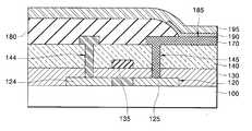
한편, 투명전극과 절연층의 경계에서 유기박막층의 불량을 방지하기 위한 절연층의 형성방법과 관련된 기술이 미국특허 5,684,365호에 제시되었다. 상기 특허에 제시된 AM 타입의 유기전계 발광표시소자의 단면 구조가 도 1에 도시되었다.Meanwhile, a technique related to a method of forming an insulating layer for preventing defects of an organic thin film layer at a boundary between a transparent electrode and an insulating layer has been disclosed in US Pat. No. 5,684,365. 1 is a cross-sectional structure of an AM type organic light emitting display device disclosed in the patent.
도 1을 참조하면, 절연기판(100)상에 소오스/드레인 영역(124), (125)을 구 비한 폴리실리콘으로 된 섬형태의 반도체층(120)이 형성되고, 반도체층(120)을 포함한 기판상에 게이트 절연막(130)이 형성되고, 게이트 절연막(130)상에 게이트(135)가 형성된다. 상기 게이트(135)를 포함한 게이트 절연막(130)상에 상기 소오스/드레인 영역(124), (125)을 노출시키는 콘택홀(144), (145)을 구비한 층간 절연막(140)이 형성된다.Referring to FIG. 1, an island-
상기 층간 절연막(140)상에는, 상기 콘택홀(144)을 통해 상기 소오스영역(124)에 연결되는 소오스전극(154)과, 상기 콘택홀(145)을 통해 상기 드레인 영역(125)에 연결되는 화소전극(170)이 형성된다.On the
그리고, 상기 화소전극(170)이 노출되도록 개구부(185)를 구비한 보호막(180)이 상기 층간 절연막(140)에 형성되고, 개부부(185)에 유기 박막층(190)이 형성되고, 유기 박막층(190)을 포함한 보호막(180)상에 음극(195)이 형성된 구조를 갖는다.In addition, a
이때, 상기 보호막(180)은 상기 화소전극(170)을 노출시키는 개구부(185)의 에지, 즉 화소전극(170) 상부의 보호막(180)이 10 내지 30°의 테이퍼 에지(tapered edge)를 갖도록 형성한다. 이러한 보호막(180)의 테이퍼 에지는 후속공정에서 형성되는 유기 박막층(190)의 접착력(adhesion)을 향상시켜 불량 발생을 방지하기 위한 것이다.In this case, the
레이저 전사법을 이용하여 유기 박막층을 제조하는 경우에는 전사된 유기 발광 재료의 전사특성 및 발광특성은 그 하부의 박막트랜지스터 기판의 구조에 많은 영향을 받는데, 칼라 패터닝 방식의 차이에 의하여 절연막의 경사각보다는 절연층 의 두께가 중요한 요소로 작용한다.In the case of manufacturing the organic thin film layer by using the laser transfer method, the transfer characteristics and emission characteristics of the transferred organic light emitting material are greatly influenced by the structure of the thin film transistor substrate below. The thickness of the insulating layer is an important factor.
본 발명은 상기한 바와같은 종래 기술의 문제점을 해결하기 위한 것으로서, 화소전극의 개구부의 에지부부분에서 발생하는 유기 EL층의 패턴불량을 방지할 수 있는 풀칼라 유기전계 발광표시소자의 제조방법을 제공하는 데 그 목적이 있다.The present invention is to solve the problems of the prior art as described above, and to provide a method for manufacturing a full color organic light emitting display device capable of preventing a pattern defect of an organic EL layer occurring at an edge portion of an opening of a pixel electrode. The purpose is to provide.
본 발명의 다른 목적은 화소전극상의 절연막을 500nm 이하의 두께를 갖도록 형성하여 화소전극의 개구부의 에지부분에서의 유기 EL층의 패턴불량을 방지할 수 있는 풀칼라 유기전계 발광표시소자의 제조방법을 제공하는 데 그 목적이 있다.Another object of the present invention is to provide a method for manufacturing a full color organic light emitting display device capable of preventing a pattern defect of an organic EL layer at an edge portion of an opening of a pixel electrode by forming an insulating film on the pixel electrode to have a thickness of 500 nm or less. The purpose is to provide.
본 발명의 다른 목적들은 상세하게 후술될 본 발명의 상세한 설명에 의하여 보다 명확해질 것이다.Other objects of the present invention will become more apparent from the following detailed description of the invention.
이와 같은 본 발명의 목적을 달성하기 위하여 본 발명은 기판상에 상기 기판과의 단차가 500nm 이하가 되도록 절연막을 형성하는 단계와; 상기 절연막을 포함한 기판상에 레이저 열 전사법에 의하여 유기박막층을 형성하는 단계를 포함하는 표시소자의 제조방법을 제공하는 것을 특징으로 한다.In order to achieve the object of the present invention, the present invention includes the steps of forming an insulating film on the substrate such that the step is 500nm or less with the substrate; It provides a method of manufacturing a display device comprising the step of forming an organic thin film layer on a substrate including the insulating film by a laser thermal transfer method.
삭제delete
삭제delete
삭제delete
삭제delete
삭제delete
삭제delete
삭제delete
삭제delete
삭제delete
삭제delete
삭제delete
삭제delete
삭제delete
삭제delete
삭제delete
삭제delete
또한, 본 발명은 기판상에 하부막을 형성하는 단계와; 상기 하부막의 에지부분에서의 두께가 500nm 이하가 되도록, 상기 하부막의 에지부분을 포함한 기판상에 절연막을 형성하는 단계와; 상기 하부막을 포함한 절연막상에 레이저 열 전사법에 의하여 유기 박막층을 형성하는 단계를 포함하는 표시소자의 제조방법을 제공하는 것을 특징으로 한다.In addition, the present invention comprises the steps of forming a lower film on the substrate; Forming an insulating film on the substrate including the edge portion of the lower layer so that the thickness at the edge portion of the lower layer is 500 nm or less; It is characterized by providing a method of manufacturing a display device comprising the step of forming an organic thin film layer on the insulating film including the lower film by a laser thermal transfer method.
또한, 본 발명은 기판상에 하부전극을 형성하는 단계와; 상기 하부전극의 에지부분에서의 두께가 500nm 이하가 되도록, 상기 하부전극의 에지부분을 포함한 기판상에 절연막을 형성하는 단계와; 상기 하부전극상에 레이저 열 전사법을 이용하여 유기 박막층을 형성하는 단계와; 상기 유기 박막층을 포함한 절연막상에 상부전극을 형성하는 단계를 포함하는 유기전계 발광표시소자의 제조방법을 제공하는 것을 특징으로 한다.In addition, the present invention comprises the steps of forming a lower electrode on the substrate; Forming an insulating film on the substrate including the edge portion of the lower electrode such that the thickness at the edge portion of the lower electrode is 500 nm or less; Forming an organic thin film layer on the lower electrode by using a laser thermal transfer method; It provides a method of manufacturing an organic light emitting display device comprising the step of forming an upper electrode on the insulating film including the organic thin film layer.
또한, 본 발명은 기판상에 소오스/드레인 전극을 구비한 박막 트랜지스터를 형성하는 단계와; 상기 박막 트랜지스터의 소오스/드레인 전극중 하나와 연결되는 화소전극을 형성하는 단계와; 상기 화소전극의 에지부분에서의 두께가 500nm 이하가 되도록, 상기 화소전극의 에지부분을 포함한 상기 기판상에 절연막을 형성하는 단계와; 상기 화소전극상에 레이저 열 전사법을 이용하여 유기 박막층을 형성하는 단계를 포함하는 유기전계 발광표시소자의 제조방법을 제공하는 것을 특징으로 한다.In addition, the present invention includes forming a thin film transistor having a source / drain electrode on the substrate; Forming a pixel electrode connected to one of the source / drain electrodes of the thin film transistor; Forming an insulating film on the substrate including the edge portion of the pixel electrode such that the thickness at the edge portion of the pixel electrode is 500 nm or less; It provides a method for manufacturing an organic light emitting display device comprising the step of forming an organic thin film layer on the pixel electrode by using a laser thermal transfer method.
상기 절연막의 두께는 바람직하게 200nm 이하이고, 보다 바람직하게 100 내지 200nm 이다. 상기 유기 박막층은 정공주입층, 정공수송층, R, G, 또는 B 발광층, 전자주입층, 전자수송층 중 하나 이상을 포함하며, 상기 유기 박막층은 레이저 전사법을 이용하여 패터닝된다.The thickness of the insulating film is preferably 200 nm or less, more preferably 100 to 200 nm. The organic thin film layer includes one or more of a hole injection layer, a hole transport layer, an R, G, or B light emitting layer, an electron injection layer, and an electron transport layer, and the organic thin film layer is patterned using a laser transfer method.
이하, 본 발명의 실시예를 첨부 도면을 참조하여 설명하면 다음과 같다.Hereinafter, an embodiment of the present invention will be described with reference to the accompanying drawings.
도 2는 본 발명의 제1실시예에 따른 PM 타입 유기전계 발광표시소자의 단면 구조를 도시한 것이다. 도 2를 참조하면, 절연기판(200)상에 ITO와 같은 투명전극의 화소전극(270)이 양극으로서 형성되고, 상기 화소전극(270)의 에지부분을 덮도록 절연막(280)이 형성되며, 상기 화소전극(270)상에 유기박막층(290)이 형성되며, 상기 유기박막층(290)을 포함한 절연막(280)상에 상부전극(295)으로서 음극이 형성된다.2 illustrates a cross-sectional structure of a PM type organic light emitting display device according to a first embodiment of the present invention. 2, a
상기 절연막(280)은 500nm 이하의 두께로 형성되는데, 바람직하게는 10 내지 500nm 이하의 두께로 형성된다. 특히, 상기 절연막(280)은 화소전극(270)의 에지부분에 형성된 부분의 두께(d2)가 500nm 이하로 되도록 형성되는데, 바람직하게는 10 내지 500nm 가 되도록 형성된다. 보다 바람직하게는, 상기 절연막(280)은 상기 화소전극(270)의 에지부분에 형성된 부분의 두께(d2)가 100 내지 200nm 가 되도록 형성된다.The insulating
상기한 바와 같은 두께를 갖는 절연막(280)상에 레이저 전사법으로 유기박막층(290)을 형성하면 도 10에서와 같이 화소전극(270)과 절연막(280)간의 경계에서의 유기박막층의 에지 불량은 발생되지 않는다. 이때, 상기 유기박막층(290)은 정공주입층(HIL, hole injection layer), 정공수송층(HTL, hole transport layer), R, G, B 유기 발광(EL, electroluminescence)층, 전자수송층(ETL, electron transport layer), 전자주입층(EIL, electron injection layer) 등을 포함한다.When the organic
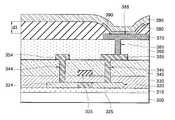
도 3은 본 발명의 제2실시예에 따른 탑 게이트 박막 트랜지스터 유기전계 발광표시소자의 단면구조를 도시한 것이다.3 illustrates a cross-sectional structure of a top gate thin film transistor organic light emitting display device according to a second exemplary embodiment of the present invention.
도 3을 참조하면, 제2실시예에 따른 유기전계 발광표시소자는 절연기판(300) 상에 버퍼층(310)이 형성되고, 상기 버퍼층(310)상에 탑 게이트구조의 박막 트랜지스터가 형성된다. 상기 박막 트랜지스터는 버퍼층(310)상에 형성된, 소오스/드레인 영역(324), (325)을 구비한 반도체층(320)과, 게이트 절연막(330)상에 형성된 게이트전극(335)과, 콘택홀(344), (345)을 통해 상기 소오스/드레인 영역(324), (325)과 전기적으로 연결되는, 층간 절연막(340)상에 형성된 소오스/드레인 전극(354), (355)을 구비한다.Referring to FIG. 3, in the organic light emitting display device according to the second embodiment, a
그리고, 상기 박막 트랜지스터가 형성된 기판 전면상에 보호막(360)이 형성되고, 상기 보호막(360)상에는 비어홀(365)을 통해 상기 소오스/드레인 전극중 하나, 예를 들면 드레인 전극(355)에 전기적으로 연결되는 화소전극(370)이 양극으로서 형성된다. 상기 화소전극(370)을 노출시키는 개구부(385)를 구비한 평탄화용 절연막(380)이 상기 화소전극(370)의 에지부분을 포함한 보호막(360)상에 형성된다. 상기 개구부(385)의 상기 화소전극(370)상에 유기 박막층(390)이 형성되고, 유기 박막층(390)을 포함한 절연막(380)상에 상부전극(395)으로서 음극이 형성된다.In addition, a
상기 절연막(380)은 500nm 이하의 두께로 형성되는데, 바람직하게는 10 내지 500nm 이하의 두께로 형성된다. 특히, 상기 절연막(380)은 화소전극(370)의 에지부분에 형성된 부분의 두께(d3)가 500nm 이하로 되도록 형성되는데, 바람직하게는 10 내지 500nm 가 되도록 형성된다. 보다 바람직하게는, 상기 절연막(380)은 상기 화소전극(370)의 에지부분에 형성된 부분의 두께(d3)가 100 내지 200nm 가 되도록 형성된다.The insulating
상기한 바와 같은 두께를 갖는 절연막(380)상에 레이저 전사법으로 유기박막 층(390)을 형성하면 도 10에서와 같이 개구부(385)의 에지 부분 즉, 화소전극(370)과 절연막(380)간의 경계에서 유기박막층의 에지 불량은 발생되지 않는다. 이때, 상기 유기박막층(390)은 정공주입층, 정공수송층, R, G, B 유기 발광층, 전자수송층, 전자주입층 등을 포함한다.If the organic
도 4은 본 발명의 제3실시예에 따른 탑 게이트 박막 트랜지스터 유기전계 발광표시소자의 단면구조를 도시한 것이다.4 illustrates a cross-sectional structure of a top gate thin film transistor organic light emitting display device according to a third exemplary embodiment of the present invention.
도 4을 참조하면, 제3실시예에 따른 유기전계 발광표시소자는 절연기판(400)상에 버퍼층(410)이 형성되고, 상기 버퍼층(410)상에 탑 게이트구조의 박막 트랜지스터가 형성된다. 상기 박막 트랜지스터는 버퍼층(410)상에 형성된, 소오스/드레인 영역(424), (425)을 구비한 반도체층(420)과, 게이트 절연막(430)상에 형성된 게이트전극(435)과, 콘택홀(444), (445)을 통해 상기 소오스/드레인 영역(424), (425)과 전기적으로 연결되는, 층간 절연막(440)상에 형성된 소오스/드레인 전극(454), (455)을 구비한다.Referring to FIG. 4, in the organic light emitting display device according to the third embodiment, a
그리고, 상기 박막 트랜지스터의 소오스/드레인 전극(454)중 하나, 예를 들면 드레인 전극(455)과 전기적으로 연결되는 화소전극(470)이 양극으로서 상기 층간 절연막(440)상에 형성된다. 상기 화소전극(470)을 노출시키는 개구부(485)를 구비한 절연막(480)이, 상기 화소전극(470)의 에지부분을 포함한 층간 절연막(440)상에 형성되는데, 상기 절연막(480)은 보호막 또는 평탄막을 위한 절연막이다. 상기 개구부(485)의 화소전극(470)상에 유기 박막층(490)이 형성되고, 유기 박막층(490)을 포함한 절연막(480)상에 상부전극(495)으로서 음극이 형성된다.One of the source /
상기 절연막(480)은 500nm 이하의 두께로 형성되는데, 바람직하게는 10 내지 500nm 이하의 두께로 형성된다. 특히, 상기 절연막(480)은 화소전극(470)의 에지부분에 형성된 부분의 두께(d4)가 500nm 이하로 되도록 형성되는데, 바람직하게는 10 내지 500nm 가 되도록 형성된다. 보다 바람직하게는, 상기 절연막(480)은 상기 화소전극(470)의 에지부분에 형성된 부분의 두께(d4)가 100 내지 200nm 가 되도록 형성된다.The insulating
상기한 바와같은 두께를 갖는 절연막(480)상에 레이저 전사법으로 유기박막층(490)을 형성하면 도 10에서와 같이 개구부(485)의 에지부분 즉, 화소전극(470)과 절연막(480)간의 경계에서 유기박막층의 에지불량은 발생되지 않는다. 이때, 상기 유기박막층(490)은 정공주입층, 정공수송층, R, G, B 유기 발광층, 전자수송층, 전자주입층을 포함한다.When the organic
도 5은 본 발명의 제4실시예에 따른 바텀 게이트 박막 트랜지스터 유기전계 발광표시소자의 단면구조를 도시한 것이다.5 illustrates a cross-sectional structure of a bottom gate thin film transistor organic light emitting display device according to a fourth exemplary embodiment of the present invention.
도 5을 참조하면, 제4실시예에 따른 유기전계 발광표시소자는 절연기판(500)상에 버퍼층(510)이 형성되고, 상기 버퍼층(510)상에 바텀 게이트구조의 박막 트랜지스터가 형성된다. 상기 박막 트랜지스터는 버퍼층(510)상에 형성된 게이트전극(535)과, 게이트 절연막(535)상에 형성된 소오스/드레인 영역(524), (525)을 구비한 반도체층(520)과, 콘택홀(544), (545)을 통해 상기 소오스/드레인 영역(524), (525)과 전기적으로 연결되는, 층간 절연막(540)상에 형성된 소오스/드레인 전극(554), (555)을 구비한다.Referring to FIG. 5, in the organic light emitting display device according to the fourth embodiment, a
그리고, 상기 박막 트랜지스터가 형성된 기판 전면상에 보호막(560)이 형성되고, 상기 보호막(560)상에는 비어홀(565)을 통해 상기 소오스/드레인 전극중 하나, 예를 들면 드레인 전극(555)에 전기적으로 연결되는 화소전극(570)이 양극으로서 형성된다. 상기 화소전극(570)을 노출시키는 개구부(585)를 구비한 평탄화용 절연막(580)이 상기 보호막(560)상에 형성된다. 상기 개구부(585)의 상기 화소전극(570)상에 유기 박막층(590)이 형성되고, 유기 박막층(590)을 포함한 절연막(580)상에 상부전극(595)으로서 음극이 형성된다.In addition, a
상기 절연막(580)은 500nm 이하의 두께로 형성되는데, 바람직하게는 10 내지 500nm 이하의 두께로 형성된다. 특히, 상기 절연막(580)은 화소전극(570)의 에지 부분에 형성된 부분의 두께(d5)가 500nm 이하로 되도록 형성되는데, 바람직하게는 10 내지 500nm 가 되도록 형성된다. 보다 바람직하게는, 상기 절연막(580)은 상기 화소전극(570)의 에지 부분에 형성된 부분의 두께(d5)가 100 내지 200nm 가 되도록 형성된다.The insulating
상기한 바와 같은 두께를 갖는 절연막(580)상에 레이저 전사법으로 유기박막층(590)을 형성하면 도 10에서와 같이 개구부(585)의 에지 부분 즉, 화소전극(570)과 절연막(580)간의 경계에서 유기박막층의 에지 불량은 발생되지 않는다. 이때, 상기 유기박막층(590)은 정공주입층, 정공수송층, R, G, B 유기 발광층, 전자수송층, 전자주입층 등을 포함한다.When the organic
도 6은 본 발명의 제5실시예에 따른 바텀 게이트 박막 트랜지스터 유기전계 발광표시소자의 단면구조를 도시한 것이다.6 illustrates a cross-sectional structure of a bottom gate thin film transistor organic light emitting display device according to a fifth embodiment of the present invention.
도 6을 참조하면, 제5실시예에 따른 유기전계 발광표시소자는 절연기판(600)상에 버퍼층(610)이 형성되고, 상기 버퍼층(610)상에 바텀 게이트구조의 박막 트랜지스터가 형성된다. 상기 박막 트랜지스터는 버퍼층(610)상에 형성된 게이트 전극(635)과, 게이트 절연막(630)상에 형성된 소오스/드레인 영역(624), (625)을 구비한 반도체층(620)과, 콘택홀(644), (645)을 통해 상기 소오스/드레인 영역(624), (625)과 전기적으로 연결되는, 층간 절연막(640)상에 형성된 소오스/드레인 전극(654), (655)을 구비한다.Referring to FIG. 6, in the organic light emitting display device according to the fifth embodiment, a
그리고, 상기 박막 트랜지스터의 소오스/드레인 전극(654)중 하나, 예를 들면 드레인 전극(655)과 전기적으로 연결되는 화소전극(670)이 양극으로서 상기 층간 절연막(640)상에 형성된다. 상기 화소전극(670)을 노출시키는 개구부(685)를 구비한 절연막(680)이 상기 화소전극(670)의 에지부분을 포함한 층간 절연막(640)상에 형성되는데, 상기 절연막(68)은 보호막 또는 평탄막을 위한 절연막이다. 상기 개구부(685)의 화소전극(670)상에 유기 박막층(690)이 형성되고, 유기 박막층(690)을 포함한 절연막(680)상에 상부전극(695)이 음극으로서 형성된다.A
상기 절연막(680)은 500nm 이하의 두께로 형성되는데, 바람직하게는 10 내지 500nm 이하의 두께로 형성된다. 특히, 상기 절연막(680)은 화소전극(670)의 에지부분에 형성된 부분의 두께(d6)가 500nm 이하로 되도록 형성되는데, 바람직하게는 10 내지 500nm 가 되도록 형성된다. 보다 바람직하게는, 상기 절연막(680)은 상기 화소전극(670)의 에지부분에 형성된 부분의 두께(d6)가 100 내지 200nm 가 되도록 형성된다.The insulating
상기한 바와같은 두께를 갖는 절연막(680)상에 레이저 전사법으로 유기박막층(690)을 형성하면 도 10에서와 같이 개구부(685)의 에지 부분 즉, 화소전극(670)과 절연막(680)간의 경계에서 유기박막층의 에지 불량은 발생되지 않는다. 이때, 상기 유기박막층(690)은 정공주입층, 정공수송층, R, G, B 유기 발광층, 전자수송층, 전자주입층 등을 포함한다.When the organic
본 발명의 실시예는 레이저 전사법을 이용하여 유기전계 발광표시소자를 제작하기 위하여, 레이저 전사법에 적합한 새로운 기판구조를 제안한다. 레이저 전사법을 이용하여 유기전계 발광표시소자를 제작하기 위해서는, 유기 EL용 고분자를 전사필름 위에 코팅 또는 증착한 후 대상 기판에 전사해야 한다. 그러므로, 전사된 유기 EL 재료의 전사 특성 및 발광 특성은 박막 트랜지스터가 형성된 기판의 구조에 많은 영향을 받는다. 따라서, 본 발명에서는 유기 박막층 바로 하부의 절연막의 두께를 한정하여 형성하여 줌으로써 레이저 전사법에 의해 유기 박막층을 불량없이 용이하게 형성하도록 하였다.The embodiment of the present invention proposes a new substrate structure suitable for the laser transfer method in order to fabricate an organic light emitting display device using the laser transfer method. In order to fabricate an organic light emitting display device using a laser transfer method, an organic EL polymer should be coated or deposited on a transfer film and then transferred to a target substrate. Therefore, the transfer characteristics and the light emission characteristics of the transferred organic EL material are greatly influenced by the structure of the substrate on which the thin film transistor is formed. Therefore, in the present invention, the thickness of the insulating film immediately below the organic thin film layer is limited, so that the organic thin film layer can be easily formed without a defect by the laser transfer method.
이하 본 발명의 실시예에 따른 유기전계 발광표시소자의 제조방법을 설명하면 다음과 같다.Hereinafter, a method of manufacturing an organic light emitting display device according to an embodiment of the present invention will be described.
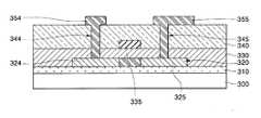
도 7a 내지 도 7d는 본 발명의 일 실시예에 따른 탑 게이트 박막 트랜지스터 유기전계 발광표시소자의 제조방법을 설명하기 위한 공정 단면도를 도시한 것이다. 본 발명의 일 실시예에 따른 제조방법은 도 3에 도시된 바와같은 단면구조를 갖는 유기전계 발광표시소자의 제조방법에 관하여 설명하는 것이다.7A through 7D are cross-sectional views illustrating a method of manufacturing a top gate thin film transistor organic light emitting display device according to an exemplary embodiment of the present invention. A manufacturing method according to an embodiment of the present invention will be described with reference to the manufacturing method of the organic light emitting display device having a cross-sectional structure as shown in FIG.
도 7a를 참조하면, AM OLED용 절연기판(300)으로서 유리기판을 세정하고, 상 기 절연기판(300)상에 버퍼층(310)으로서 SiO2를 형성하고, 상기 버퍼층(310)상에 폴리실리콘막으로 된 반도체층(320)을 형성한다. 상기 반도체층(320)의 형성방법은 예를 들면, 상기 버퍼층(310)상에 비정질 실리콘막을 PECVD를 이용하여 증착하고, 엑시머 레이저를 이용하여 상기 증착된 비정질 실리콘막을 폴리실리콘막으로 결정화하며, 결정화된 폴리실리콘막을 패터닝하여 섬형태의 반도체층(320)을 형성한다.Referring to FIG. 7A, the glass substrate is cleaned as the insulating
이어서, 상기 반도체층(320)을 포함한 버퍼층(310)상에 SiO2 와 같은 게이트 절연막(330)을 형성하고, 상기 반도체층(320)에 대응하는 상기 게이트 절연막(330)상에 게이트 전극(335)을 형성한다. 상기 게이트 전극(335)을 마스크로 하여 상기 반도체층(320)으로 소정 도전형, 예를 들면, n형 또는 p형 불순물중 하나를 이온주입하여 소오스/드레인 영역(324), (325)을 형성한다.Subsequently, a
다음, 기판전면에 SiNx 와 같은 층간 절연막(340)을 형성하고, 상기 층간 절연막(340)과 게이트 절연막(330)을 식각하여 상기 소오스/드레인 영역(324), (325)을 각각 노출시키는 콘택홀(344), (345)을 형성한다. 층간 절연막(340)상에 소오스/드레인 전극물질을 증착한 다음 패터닝하여 상기 콘택홀(344), (345)을 통해 상기 소오스/드레인 영역(324), (325)과 각각 콘택되는 소오스/드레인 전극(354), (355)을 형성한다.Next, a contact that exposes the source /
도 7b를 참조하면, 상기 소오스/드레인 전극(354), (355)을 포함한 층간 절연막(340)상에 SiO2와 같은 보호막(360)을 형성하고, 상기 보호막(360)을 식각하여 상기 소오스/드레인 전극(354), (355)중 하나, 예를 들면 드레인 전극(355)을 노출 시키는 비어홀(365)을 형성한다.Referring to FIG. 7B, a
이어서, 상기 비어홀(365)을 포함한 보호막(360)상에 투명도전막, 예를 들면 ITO를 200 nm의 두께로 스퍼터링하여 증착하고, 건식식각하여 양극으로서 화소전극(370)을 형성한다.Subsequently, a transparent conductive film, for example, ITO, is deposited on the
이어서, 상기 층간 절연막(360)상에 상기 화소전극(370)의 에지부분을 덮도록 평탄화용 절연막(380)을 형성하는 데, 아크릴을 1300rpm의 속도로 350nm의 두께로 스핀코팅하고 패터닝하여 개구부(385)를 한정하며 이어서 220℃ 에서 베이킹하여, 최종적으로 상기 화소전극(370)의 에지부분에 형성된 부분이 소정의 두께(d3), 예를 들면 250nm 의 두께를 갖으며, 개구부(385)의 에지부분에서 15°의 경사각을 갖는 절연막(380)을 형성한다.Subsequently, a
도 7c 및 도 7d 는 레이저 전사법을 이용하여 개구부(385)내의 화소전극(370)상에 유기박막층(390)을 형성하는 공정으로서, 먼저 PEDOT을 3000 rpm으로 50nm 의 두께로 스핀코팅하고 200℃에서 5분동안 열처리하여 정공수송층(390a)을 형성한다. 이어서, R, G, B 발광층을 위한 3매의 전사필름을 제조하는데, 본 발명의 실시예에서는 R, G, B 발광층을 위한 3매의 전사필름중 1매의 전사필름, 예를 들면 R 발광층을 위한 전사필름(30)에 대하여 설명한다.7C and 7D illustrate a process of forming the organic
광흡수층(32)이 형성된 베이스 필름(31)상에 발광층 형성물질인 R 칼라를 각각 1.0wt/V% 의 농도의 크실렌(xylene) 용액을 이용하여 2000 rpm의 속도로 스핀코팅하여 80 nm의 두께를 갖는 R 칼라를 위한 전사층(33)을 형성하여 전사필름(30)을 제조한다.80 nm of the R color, which is a light emitting layer forming material, was spin-coated at a speed of 2000 rpm using a xylene solution having a concentration of 1.0 wt / V% on the
전사필름(30)을 정공수송층(390a)이 코팅된 기판상에 진공으로 고정한 후 적외선(IR, infrared radiation) 레이저(35)를 이용하여 원하는 패턴으로 전사하여 R 발광층(390b)를 형성한다. 이로써, 정공수송층(390a)과 R 발광층(390b)을 구비한 유기 박막층(390)이 형성된다.After the
상기한 바와같은 방법으로 G, B 칼라를 위한 전사필름을 제조하여 전사하면 R, G, B 풀칼라를 위한 유기 박막층(390)이 형성되고, 상기 유기 박막층(390)은 상기 R, G, B 유기 발광층과 정공수송층 외에 정공주입층, 전자 주입층, 전자수송층을 더 포함할 수도 있다.When the transfer film for G and B colors is manufactured and transferred in the same manner as described above, an organic
최종적으로, 유기 박막층(390)을 레이저 전사법을 이용하여 패터닝한 후 Ca/Ag를 각각 30 nm, 270 nm의 두께로 증착하여 음극으로서 상부전극(395)을 형성한다. 이후 봉지방법에 의해 봉지하여 AM OLED를 제작한다. 상기한 바와같이 제작된 유기전계 발광표시소자는 유기박막층 하부의 절연막의 두께를 500nm 이하로 형성하여 줌으로써, 개구부에 레이저 전사법으로 전사된 R, G, B 발광층이 뜯어지는 불량을 방지하게 된다.Finally, after the organic
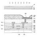
도 8a 내지 도 8d는 본 발명의 다른 실시예에 따른 바텀 게이트 박막 트랜지스터 유기전계 발광표시소자의 제조방법을 설명하기 위한 공정 단면도를 도시한 것이다. 본 발명의 다른 실시예에 따른 제조방법은 도 5에 도시된 바와같은 단면구조를 갖는 유기전계 발광표시소자의 제조방법에 관하여 설명하는 것이다.8A through 8D are cross-sectional views illustrating a method of manufacturing a bottom gate thin film transistor organic light emitting display device according to another exemplary embodiment of the present invention. A manufacturing method according to another embodiment of the present invention will be described with reference to the manufacturing method of the organic light emitting display device having a cross-sectional structure as shown in FIG.
도 8a를 참조하면, AM OLED용 절연기판(500)으로서 유리기판을 세정하고, 상 기 절연기판(500)상에 버퍼층(510)으로서 SiO2를 형성하며, 상기 버퍼층(510)상에 게이트전극(535)을 형성한다. 상기 게이트 전극(535)을 포함한 버퍼층(510)상에 게이트 절연막(530)을 형성하고, 상기 게이트 전극(535)에 대응하는 게이트 절연막(530)상에 폴리실리콘막으로 된 반도체층(520)을 형성한다. 상기 반도체층(520)의 형성방법은 예를 들면, 상기 버퍼층(510)상에 비정질 실리콘막을 PECVD를 이용하여 증착하고, 엑시머 레이저를 이용하여 상기 증착된 비정질 실리콘막을 폴리실리콘막으로 결정화하며, 결정화된 폴리실리콘막을 패터닝하여 섬형태의 반도체층(520)을 형성한다.Referring to FIG. 8A, a glass substrate is cleaned with an AM
이어서, 상기 반도체층(520)으로 소정 도전형, 예를 들면, n형 또는 p형 불순물중 하나를 이온주입하여 소오스/드레인 영역(524), (525)을 형성한다. 기판전면에 SiNx 와 같은 층간 절연막(540)을 형성하고, 상기 층간 절연막(540)과 게이트 절연막(530)을 식각하여 상기 소오스/드레인 영역(524), (525)을 각각 노출시키는 콘택홀(544), (545)을 형성한다. 층간 절연막(540)상에 소오스/드레인 전극물질을 증착한 다음 패터닝하여 상기 콘택홀(544), (545)을 통해 상기 소오스/드레인 영역(524), (525)과 각각 콘택되는 소오스/드레인 전극(554), (555)을 각각 형성한다.Subsequently, source /
도 8b 에 도시된 바와같이, 상기 소오스/드레인 전극(554), (555)을 포함한 층간 절연막(540)상에 보호막(560)으로 SiO2를 형성하고, 상기 보호막(560)을 패터닝하여 상기 소오스/드레인 전극(554), (555)중 하나, 예를 들면 드레인 전극(555) 을 노출시키는 비어홀(565)을 형성한다. 상기 비어홀(565)을 포함한 보호막(560)상에 투명도전막으로 ITO막을 200nm 의 두께로 스퍼터 증착하고 패터닝하여 양극으로서 화소전극(570)을 형성한다.As shown in FIG. 8B, SiO2 is formed as a
이어서, 상기 보호막(560)상에 상기 화소전극(570)의 에지부분을 덮도록 개구부(585)를 구비한 평탄화용 절연막(580)을 형성하는 데, 아크릴을 1300rpm의 속도로 350nm의 두께로 스핀코팅하고 패터닝하여 개구부(585)를 한정하며 220℃ 에서 베이킹하여, 최종적으로 상기 화소전극(370)의 에지부분에 형성된 부분의 두께(d5)가 250nm 가 되고, 개구부(585)의 에지부분에서 15°의 경사각을 갖는 절연막(580)을 형성한다.Subsequently, a
도 8c 및 도 8d는 레이저 전사법으로 풀칼라 유기박막층(590)을 형성하는 공정으로서, 먼저 기판전면에 정공수송층(590a)을 형성하는데, PEDOT을 3000 rpm으로 50nm 의 두께로 스핀코팅하고 200℃에서 5분동안 열처리하여 정공수송층(590a)을 형성한다. 이어서, R, G, B 발광층을 위한 3매의 전사필름을 제조하는데, 본 발명의 실시예에서는 R, G, B 발광층을 위한 3매의 전사필름중 1매의 전사필름, 예를 들면 R 발광층을 위한 전사필름(50)에 대하여 설명한다.8C and 8D illustrate a process of forming a full-color organic
광흡수층(52)을 구비한 베이스필름(51)상에 발광층 형성물질인 R 칼라를 1.0wt/V% 의 농도의 크실렌 용액을 이용하여 2000 rpm의 속도로 스핀코팅하여 80 nm의 두께를 갖는 전사층(53)을 형성하여 전시필름(50)을 제조한다. 이어서, R전사필름(50)을 정공수송층(590a)이 코팅된 기판상에 진공으로 고정한 후 IR 레이저(55)를 이용하여 원하는 패턴으로 전사하여 R 발광층(590b)을 형성한다. 이 로써, 정공수송층(590a)과 R 발광층(590b)을 구비한 유기 박막층(590)이 형성된다.Transfer coating having a thickness of 80 nm on the
상기한 바와같은 방법으로 G, B 칼라를 위한 전사필름을 제조하여 전사하면 R, G, B 풀칼라를 위한 유기 박막층(590)이 형성되고, 상기 유기 박막층(590)은 상기 R, G, B 유기 발광층과 정공수송층 외에 정공주입층, 전자 주입층, 전자수송층을 더 포함할 수도 있다.When the transfer film for G and B colors is manufactured and transferred in the same manner as described above, an organic
최종적으로 유기 박막층(590)을 레이저 전사법을 이용하여 패터닝한 후 Ca/Ag를 각각 30 nm, 270 nm의 두께로 증착하여 음극으로서 상부전극(595)을 형성한다. 이후 봉지방법에 의해 봉지하여 AM OLED를 제작한다. 상기한 바와같이 제작된 유기전계 발광표시소자는 유기박막층 하부의 절연막의 두께를 500nm 이하로 형성하여 줌으로써, 개구부에 레이저 전사법으로 전사된 R, G, B 발광층이 뜯어지는 불량은 방지된다.Finally, the organic
본 발명의 실시예에 따른 유기전계 발광표시소자의 제조공정은 도 3 및 도 5에 도시된 바와같은 단면구조를 갖는 소자에 관하여 설명하였으나, 도 4 및 도 6에 도시된 바와같은 단면구조를 갖는 소자에 대해서도 동일하게 적용될 수 있다. 도 4에 도시된 소자의 경우에는 층간 절연막(440)상에 소오스/드레인 전극(454, 455)을 형성하고, 상기 층간 절연막(440)상에 상기 드레인 전극(455)에 연결되는 화소전극(470)을 형성한다.The manufacturing process of the organic light emitting display device according to the embodiment of the present invention has been described with reference to the device having a cross-sectional structure as shown in FIGS. 3 and 5, but has a cross-sectional structure as shown in FIGS. 4 and 6. The same can be applied to the device. In the device illustrated in FIG. 4, source /
이어서, 드레인 전극(455)과 화소전극(470)을 분리시켜 주기 위한 보호막의 형성공정없이 바로 층간 절연막(440)상에 보호막 또는 평탄화막을 위한 절연막(480)으로 아크릴을 상기 제조공정에서 설명한 바와같은 방법으로 제조한다.Subsequently, acryl was used as the insulating
도 4에 적용되는 공정은 도 6에 도시된 단면구조를 갖는 소자에도 동일하게 적용할 수 있다.The process applied to FIG. 4 can be equally applied to an element having a cross-sectional structure shown in FIG. 6.
도 9는 도 1에 도시된 종래의 유기전계 발광표시소자에 있어서, 레이저 전사법을 이용하여 R, G, B 의 유기박막층을 패터닝할 때, 화소전극(170)의 에지부분상에 형성된 절연막(180)이 그의 두께가 500 ~ 1000nm 의 범위에서 형성되거나 혹은 그 이상으로 형성될 때 나타나는 불량(F)의 형태를 보여주고 있다. 즉, 절연막의 경계부분에서 뜯어진 불량이나 다수의 픽셀의 경계면에 걸쳐 뜯어지는 불량, 에지부터 픽셀내부에까지 뜯어진 불량, 혹은 경계면이 지저분하게 뜯겨져 있는 불량등을 보여준다.9 is a view illustrating an insulating film formed on an edge portion of a
도 10은 본 발명의 실시예에 따른 유기전계 발광표시소자에 있어서, 유기박막층의 패턴을 보여주는 도면이다. 본 발명의 실시예에서와 같이 화소전극의 에지부분상에 형성되는 절연막을 그의 두께가 500 nm 이하 바람직하게는 200nm 이하로 형성한 경우에는 도 10에서와 같이 안정적인 칼라패턴을 얻을 수 있음을 알 수 있다.10 is a view illustrating a pattern of an organic thin film layer in an organic light emitting display device according to an exemplary embodiment of the present invention. As in the embodiment of the present invention, when the insulating film formed on the edge portion of the pixel electrode is formed to have a thickness of 500 nm or less, preferably 200 nm or less, a stable color pattern can be obtained as shown in FIG. 10. have.
본 발명에서는 레이저 전사법에 의해 유기 EL층을 패터닝할 때 열과 압력에 의하여 전사필름상에 존재하는 발광층 형성물질을 기판으로 전사하게 되는데, 50 내지 100nm 의 두께를 갖는 발광층 형성물질을 포함하는 전사필름은 개구부에서 절연막과 하부전극인 투명전극간에 단차가 클 경우에는, 예를 들어 500nm 이상인 경우에는 기판에 밀착되지 않고 떠있는 상태가 된다.In the present invention, when the organic EL layer is patterned by the laser transfer method, the light emitting layer forming material existing on the transfer film is transferred to the substrate by heat and pressure, and the transfer film includes a light emitting layer forming material having a thickness of 50 to 100 nm. If the step is large between the insulating film and the transparent electrode as the lower electrode in the silver opening, for example, 500 nm or more, the state becomes floating without being in close contact with the substrate.
이런 상태에서 레이저 전사시 가해지는 열과 압력에 의해 개구부의 절연막과 투명전극의 에지부분에서 유기 박막층이 찢어지게 되며, 전사가 불완전하게 되어 도 9에서와 같은 불량이 발생하는 것이다.In this state, the organic thin film layer is torn at the edge of the insulating film and the transparent electrode of the opening due to the heat and pressure applied during the laser transfer, and the transfer is incomplete, resulting in a defect as shown in FIG. 9.
따라서, 본 발명에서는 이러한 불량을 제거하기 위하여 절연막과 하부전극간의 단차가 500nm 이하가 되도록 절연막의 두께를 조절하여 도 10과 같이 불량의 발생을 방지하여 주는 것이다.Therefore, in the present invention, the thickness of the insulating film is adjusted to prevent the defect from occurring as shown in FIG.
유기전계 발광표시소자에서, 투명전극의 상부에 형성되는 절연막은 표면을 평탄화하기 위한 것으로, 그의 상부에 형성되는 상부전극인 음극과의 사이에 발생될 수도 있는 기생 캐패시턴스를 방지하기 위하여 종래에는 1㎛ 이상의 두께로 형성하였으나, 본 발명에서와 같이 절연막의 두께를 500nm 이하로 형성하여도 기생 캐패시턴스 문제는 발생되지 않는다.In an organic light emitting display device, an insulating film formed on an upper portion of a transparent electrode is used to planarize a surface, and in order to prevent parasitic capacitance that may be generated between a cathode, which is an upper electrode formed on an upper portion thereof, 1 μm is conventionally used. Although formed to the above thickness, the parasitic capacitance problem does not occur even when the thickness of the insulating film is formed to 500 nm or less as in the present invention.
이상에서 상세하게 설명한 바와같은 본 발명에 따르면, 유기박막층 하부에 형성되는 절연막을 500nm 이하의 두께로 형성하여 줌으로써, 레이저 전사법에 의한 유기박막층의 패터닝시, 개구부의 에지부분 즉, 절연막과 투명전극간의 경계에서 유기박막층의 에지불량을 방지할 수 있으며, 이에 따라 화소전극의 에지부분에서의 칼라패턴의 이미지 특성을 향상시킬 수 있는 이점이 있다. 또한, 상대적으로 절연막의 두께가 얇아지므로, 유기전계 발광표시소자의 특성을 향상시킬 수 있는 이점이 있다.According to the present invention as described in detail above, by forming an insulating film formed below the organic thin film layer to a thickness of 500nm or less, when the organic thin film layer is patterned by the laser transfer method, the edge portion of the opening, that is, the insulating film and the transparent electrode Edge defects of the organic thin film layer can be prevented at the boundary between them, thereby improving the image characteristic of the color pattern at the edge portion of the pixel electrode. In addition, since the thickness of the insulating film is relatively thin, there is an advantage that the characteristics of the organic light emitting display device can be improved.
또한, 본 발명은 PM 타입의 유기전계 발광표시소자, 각각의 R, G, B 발광층을 채용하는 서브 픽셀내에 두 개이상의 박막 트랜지스터를 구비하는 AM 타입의 유 기전계 발광표시소자에 적용가능할 뿐만 아니라 레이저 전사법을 이용하는 칼라패턴사이에 격벽을 구비한 표시소자에 모두 적용가능한 이점이 있다.In addition, the present invention is not only applicable to PM type organic light emitting display devices, and AM type organic light emitting display devices having two or more thin film transistors in sub-pixels employing respective R, G, and B light emitting layers. There is an advantage that all of the display elements having partitions between the color patterns using the laser transfer method can be applied.
상기에서는 본 발명의 바람직한 실시예를 참조하여 설명하였지만, 해당 기술 분야의 숙련된 당업자는 하기의 특허 청구의 범위에 기재된 본 발명의 사상 및 영역으로부터 벗어나지 않는 범위 내에서 본 발명을 다양하게 수정 및 변경시킬 수 있음을 이해할 수 있을 것이다.Although described above with reference to a preferred embodiment of the present invention, those skilled in the art will be variously modified and changed within the scope of the invention without departing from the spirit and scope of the invention described in the claims below I can understand that you can.
Claims (66)
Translated fromKoreanPriority Applications (10)
| Application Number | Priority Date | Filing Date | Title |
|---|---|---|---|
| KR1020010073822AKR100656490B1 (en) | 2001-11-26 | 2001-11-26 | Full color organic light emitting display device and manufacturing method thereof |
| US10/167,420US7009339B2 (en) | 2001-11-26 | 2002-06-13 | Organic EL display device and method of manufacturing the same |
| EP02090385AEP1315209A3 (en) | 2001-11-26 | 2002-11-20 | Organic EL display device and method of manufacturing the same |
| JP2002338475AJP4071606B2 (en) | 2001-11-26 | 2002-11-21 | Manufacturing method of full-color organic electroluminescence display device |
| CNB021526109ACN1279794C (en) | 2001-11-26 | 2002-11-26 | Organic electroluminescence display and manufacturing method thereof |
| US11/011,596US8142839B2 (en) | 2001-11-26 | 2004-12-15 | Method for fabricating a display device |
| US11/011,595US7705534B2 (en) | 2001-11-26 | 2004-12-15 | Organic EL display device |
| US11/175,183US7696689B2 (en) | 2001-11-26 | 2005-07-07 | Organic EL display device having an organic EL layer formed on an exposed underlying layer |
| US11/312,547US8153184B2 (en) | 2001-11-26 | 2005-12-21 | Organic EL display device and method of manufacturing the same |
| JP2007167959AJP2007280963A (en) | 2001-11-26 | 2007-06-26 | Full-color organic electroluminescence display device |
Applications Claiming Priority (1)
| Application Number | Priority Date | Filing Date | Title |
|---|---|---|---|
| KR1020010073822AKR100656490B1 (en) | 2001-11-26 | 2001-11-26 | Full color organic light emitting display device and manufacturing method thereof |
Related Child Applications (1)
| Application Number | Title | Priority Date | Filing Date |
|---|---|---|---|
| KR1020050035746ADivisionKR100574089B1 (en) | 2005-04-28 | 2005-04-28 | Full color organic light emitting display device and manufacturing method thereof |
Publications (2)
| Publication Number | Publication Date |
|---|---|
| KR20030042937A KR20030042937A (en) | 2003-06-02 |
| KR100656490B1true KR100656490B1 (en) | 2006-12-12 |
Family
ID=37421614
Family Applications (1)
| Application Number | Title | Priority Date | Filing Date |
|---|---|---|---|
| KR1020010073822AExpired - LifetimeKR100656490B1 (en) | 2001-11-26 | 2001-11-26 | Full color organic light emitting display device and manufacturing method thereof |
Country Status (5)
| Country | Link |
|---|---|
| US (4) | US7009339B2 (en) |
| EP (1) | EP1315209A3 (en) |
| JP (2) | JP4071606B2 (en) |
| KR (1) | KR100656490B1 (en) |
| CN (1) | CN1279794C (en) |
Cited By (1)
| Publication number | Priority date | Publication date | Assignee | Title |
|---|---|---|---|---|
| US12022692B2 (en) | 2021-01-18 | 2024-06-25 | Samsung Display Co., Ltd. | Light emitting display device having reduced interference between adjacent pixels |
Families Citing this family (59)
| Publication number | Priority date | Publication date | Assignee | Title |
|---|---|---|---|---|
| US8153184B2 (en)* | 2001-11-26 | 2012-04-10 | Samsung Mobile Display Co., Ltd. | Organic EL display device and method of manufacturing the same |
| KR100656490B1 (en)* | 2001-11-26 | 2006-12-12 | 삼성에스디아이 주식회사 | Full color organic light emitting display device and manufacturing method thereof |
| KR100421720B1 (en)* | 2001-12-13 | 2004-03-11 | 삼성 엔이씨 모바일 디스플레이 주식회사 | Electro luminescence device and method of manufacturing the same |
| JP4170700B2 (en)* | 2002-07-31 | 2008-10-22 | 大日本印刷株式会社 | Electroluminescence display device and manufacturing method |
| GB2391686B (en)* | 2002-07-31 | 2006-03-22 | Dainippon Printing Co Ltd | Electroluminescent display and process for producing the same |
| JP4251874B2 (en)* | 2003-01-21 | 2009-04-08 | 三洋電機株式会社 | Electroluminescence display device |
| US7275972B2 (en)* | 2003-08-22 | 2007-10-02 | 3M Innovative Properties Company | Method of making an electroluminescent device having a patterned emitter layer and non-patterned emitter layer |
| KR100741962B1 (en) | 2003-11-26 | 2007-07-23 | 삼성에스디아이 주식회사 | Flat Panel Display |
| KR100611156B1 (en)* | 2003-11-29 | 2006-08-09 | 삼성에스디아이 주식회사 | Donor substrate for laser transfer and organic electroluminescent element manufactured using the substrate |
| KR100611159B1 (en)* | 2003-11-29 | 2006-08-09 | 삼성에스디아이 주식회사 | Organic light emitting display device |
| WO2005111972A1 (en)* | 2004-05-13 | 2005-11-24 | Ulvac, Inc. | Display, and method for fabricating same |
| US8278818B2 (en) | 2004-06-04 | 2012-10-02 | Samsung Mobile Display Co., Ltd. | Electroluminescent display device and method of fabricating the same |
| KR100659757B1 (en)* | 2004-08-25 | 2006-12-19 | 삼성에스디아이 주식회사 | Organic electroluminescent device and manufacturing method thereof |
| JP2006086069A (en) | 2004-09-17 | 2006-03-30 | Three M Innovative Properties Co | Organic electroluminescence device and method for manufacturing the same |
| KR20060026776A (en)* | 2004-09-21 | 2006-03-24 | 삼성에스디아이 주식회사 | Organic electroluminescent device and manufacturing method thereof |
| KR100699998B1 (en)* | 2004-09-23 | 2007-03-26 | 삼성에스디아이 주식회사 | Organic electroluminescent device and manufacturing method thereof |
| DE602005003425T2 (en) | 2004-10-11 | 2008-10-02 | Samsung SDI Co., Ltd., Suwon | Organic electroluminescent device and its production method |
| KR100685404B1 (en)* | 2004-10-11 | 2007-02-22 | 삼성에스디아이 주식회사 | Organic light emitting display device and manufacturing method |
| KR100700642B1 (en)* | 2004-12-13 | 2007-03-27 | 삼성에스디아이 주식회사 | Organic light emitting display device and manufacturing method thereof |
| KR100685804B1 (en)* | 2004-12-14 | 2007-02-22 | 삼성에스디아이 주식회사 | Organic Electroluminescence Device and Fabricating Method of the same |
| KR100685811B1 (en) | 2005-01-04 | 2007-02-22 | 삼성에스디아이 주식회사 | Organic light emitting display device and manufacturing method thereof |
| WO2006115283A1 (en)* | 2005-04-25 | 2006-11-02 | Showa Denko K. K. | Method of producing a display device |
| US7799509B2 (en)* | 2005-06-04 | 2010-09-21 | Samsung Electronics Co., Ltd. | Photosensitive resin composition, method of manufacturing a thin-film transistor substrate, and method of manufacturing a common electrode substrate using the same |
| KR101326595B1 (en)* | 2005-06-04 | 2013-11-20 | 주식회사 동진쎄미켐 | Photosensitive resin composition and method of manufacturing a thin film transistor substrate and method of manufacturing a common electrode substrate using the same |
| KR100711876B1 (en)* | 2005-07-05 | 2007-04-25 | 삼성에스디아이 주식회사 | Light-emitting display device and manufacturing method |
| WO2007011061A1 (en) | 2005-07-22 | 2007-01-25 | Semiconductor Energy Laboratory Co., Ltd. | Semiconductor device |
| WO2007013692A1 (en)* | 2005-07-29 | 2007-02-01 | Matsushita Electric Industrial Co., Ltd. | Organic electroluminescence element, exposure device and image forming apparatus |
| KR100645534B1 (en) | 2005-08-12 | 2006-11-14 | 삼성에스디아이 주식회사 | Laser thermal transfer mask and manufacturing method of organic electroluminescent device using same |
| KR100742370B1 (en)* | 2005-11-28 | 2007-07-24 | 삼성에스디아이 주식회사 | Manufacturing method of organic light emitting display device |
| US7601567B2 (en)* | 2005-12-13 | 2009-10-13 | Samsung Mobile Display Co., Ltd. | Method of preparing organic thin film transistor, organic thin film transistor, and organic light-emitting display device including the organic thin film transistor |
| JP4544168B2 (en)* | 2006-02-01 | 2010-09-15 | セイコーエプソン株式会社 | ORGANIC ELECTROLUMINESCENT DEVICE, ITS MANUFACTURING METHOD, AND ELECTRONIC DEVICE |
| KR100782465B1 (en)* | 2006-05-18 | 2007-12-05 | 삼성에스디아이 주식회사 | Laser thermoelectric donor substrate and manufacturing method of organic light emitting display device using the same |
| JP4438782B2 (en)* | 2006-08-23 | 2010-03-24 | ソニー株式会社 | Display device manufacturing method and display device |
| KR100770104B1 (en)* | 2006-09-28 | 2007-10-24 | 삼성에스디아이 주식회사 | Organic electroluminescent display, manufacturing method thereof and transport device for same |
| KR100824881B1 (en)* | 2006-11-10 | 2008-04-23 | 삼성에스디아이 주식회사 | Organic electroluminescent display and manufacturing method thereof |
| KR100824880B1 (en) | 2006-11-10 | 2008-04-23 | 삼성에스디아이 주식회사 | Organic electroluminescent display and manufacturing method thereof |
| KR100824902B1 (en) | 2006-12-13 | 2008-04-23 | 삼성에스디아이 주식회사 | Organic electroluminescent display and manufacturing method thereof |
| JP4396864B2 (en) | 2007-03-14 | 2010-01-13 | ソニー株式会社 | Display device and manufacturing method thereof |
| JP2008276211A (en)* | 2007-04-05 | 2008-11-13 | Fujifilm Corp | Organic electroluminescent display device and patterning method |
| KR20090092051A (en) | 2008-02-26 | 2009-08-31 | 삼성모바일디스플레이주식회사 | Organic light emitting diode and fabrication method for the same |
| EP2299784A4 (en)* | 2008-06-16 | 2012-05-30 | Toray Industries | CONTOUR MODELING METHOD, DEVICE MANUFACTURING METHOD USING THE CONTOUR MODELING METHOD, AND DEVICE |
| KR20100007266A (en)* | 2008-07-11 | 2010-01-22 | 삼성모바일디스플레이주식회사 | Organic light emitting display apparatus and method of manufacturing thereof |
| JP4912437B2 (en)* | 2008-08-05 | 2012-04-11 | 三星モバイルディスプレイ株式會社 | Organic light emitting display |
| JP2010257670A (en)* | 2009-04-23 | 2010-11-11 | Toppan Printing Co Ltd | Organic electroluminescence display panel and manufacturing method thereof |
| JP5515660B2 (en)* | 2009-11-13 | 2014-06-11 | セイコーエプソン株式会社 | Manufacturing method of substrate for semiconductor device |
| KR101202352B1 (en) | 2010-07-19 | 2012-11-16 | 삼성디스플레이 주식회사 | Organic light emitting display device and method for manufacturing the same |
| CN103780217B (en)* | 2011-02-16 | 2017-05-17 | 株式会社村田制作所 | Electronic component |
| JP2014096568A (en)* | 2012-10-10 | 2014-05-22 | Rohm Co Ltd | Organic el device |
| KR20140107036A (en)* | 2013-02-27 | 2014-09-04 | 삼성디스플레이 주식회사 | Organic light emitting diode display and menufacturing method thereof, and donor substrate |
| US8997187B2 (en) | 2013-03-15 | 2015-03-31 | Airwatch Llc | Delegating authorization to applications on a client device in a networked environment |
| JP6217183B2 (en)* | 2013-07-01 | 2017-10-25 | セイコーエプソン株式会社 | LIGHT EMITTING DEVICE AND ELECTRONIC DEVICE |
| CN104576688B (en)* | 2013-10-10 | 2018-11-09 | 精工爱普生株式会社 | Light-emitting device and electronic equipment |
| US20150129842A1 (en)* | 2013-11-13 | 2015-05-14 | Shenzhen China Star Optoelectronics Technology Co. Ltd. | Method For Manufacturing Organic Electroluminescence Device And Organic Electroluminescence Device Manufactured With Same |
| CN103560211B (en)* | 2013-11-13 | 2017-04-05 | 深圳市华星光电技术有限公司 | The preparation method of organic electroluminescence device and the organic electroluminescence device of making |
| CN105449127B (en)* | 2016-01-04 | 2018-04-20 | 京东方科技集团股份有限公司 | Diode displaying substrate and preparation method thereof, display device |
| KR102794829B1 (en)* | 2016-08-18 | 2025-04-11 | 삼성디스플레이 주식회사 | Display device and manufacturing method thereof |
| CN107393828A (en)* | 2017-07-12 | 2017-11-24 | 武汉华星光电技术有限公司 | The preparation method and thin film transistor (TFT) of thin film transistor (TFT) |
| CN109656069A (en)* | 2017-10-11 | 2019-04-19 | 京东方科技集团股份有限公司 | Production method, array substrate and the display device of array substrate |
| TWI662730B (en)* | 2018-03-09 | 2019-06-11 | 謙華科技股份有限公司 | Thermal transfer film for preparing organic light emitting diode and preparation method thereof |
Citations (5)
| Publication number | Priority date | Publication date | Assignee | Title |
|---|---|---|---|---|
| KR19980078049A (en)* | 1997-04-24 | 1998-11-16 | 구자홍 | Multicolor electroluminescent display array panel and manufacturing method thereof |
| JP2000260570A (en)* | 1999-03-11 | 2000-09-22 | Tdk Corp | Thin-film el element and its manufacture |
| KR20010057124A (en)* | 1999-12-18 | 2001-07-04 | 이형도 | Organic light emitting device having double barrier quantum well structure |
| KR20010056710A (en)* | 1999-12-16 | 2001-07-04 | 오길록 | Fabrication method of organic eletroluminescence display |
| KR20010062985A (en)* | 1999-12-21 | 2001-07-09 | 오길록 | An organic eletroluminescence device |
Family Cites Families (47)
| Publication number | Priority date | Publication date | Assignee | Title |
|---|---|---|---|---|
| US5256506A (en) | 1990-10-04 | 1993-10-26 | Graphics Technology International Inc. | Ablation-transfer imaging/recording |
| JP2734464B2 (en)* | 1990-02-28 | 1998-03-30 | 出光興産株式会社 | Electroluminescence device and method of manufacturing the same |
| US5220348A (en) | 1991-08-23 | 1993-06-15 | Eastman Kodak Company | Electronic drive circuit for multi-laser thermal printer |
| US5290418A (en)* | 1992-09-24 | 1994-03-01 | Applied Biosystems, Inc. | Viscous electrophoresis polymer medium and method |
| US5278023A (en) | 1992-11-16 | 1994-01-11 | Minnesota Mining And Manufacturing Company | Propellant-containing thermal transfer donor elements |
| JP3250583B2 (en) | 1992-11-16 | 2002-01-28 | キヤノン株式会社 | Photovoltaic element and power generation system |
| DE69309310T2 (en) | 1993-01-21 | 1997-11-06 | Merrell Pharmaceuticals Inc., Cincinnati, Ohio | DIARYLALKYL PIPERIDINE AS A MEDICINE AGAINST MULTIPLE RESISTANT TUMOR USE |
| US5308737A (en) | 1993-03-18 | 1994-05-03 | Minnesota Mining And Manufacturing Company | Laser propulsion transfer using black metal coated substrates |
| US5521035A (en) | 1994-07-11 | 1996-05-28 | Minnesota Mining And Manufacturing Company | Methods for preparing color filter elements using laser induced transfer of colorants with associated liquid crystal display device |
| US6057067A (en) | 1994-07-11 | 2000-05-02 | 3M Innovative Properties Company | Method for preparing integral black matrix/color filter elements |
| US5684365A (en) | 1994-12-14 | 1997-11-04 | Eastman Kodak Company | TFT-el display panel using organic electroluminescent media |
| US5725989A (en) | 1996-04-15 | 1998-03-10 | Chang; Jeffrey C. | Laser addressable thermal transfer imaging element with an interlayer |
| US5998085A (en) | 1996-07-23 | 1999-12-07 | 3M Innovative Properties | Process for preparing high resolution emissive arrays and corresponding articles |
| KR100195175B1 (en) | 1996-12-23 | 1999-06-15 | 손욱 | Electroluminescence element and its manufacturing method |
| US5990629A (en)* | 1997-01-28 | 1999-11-23 | Casio Computer Co., Ltd. | Electroluminescent display device and a driving method thereof |
| KR200156710Y1 (en) | 1997-03-28 | 1999-09-01 | 박병기 | Prefab Bathroom Furniture |
| JP3633229B2 (en) | 1997-09-01 | 2005-03-30 | セイコーエプソン株式会社 | LIGHT EMITTING DEVICE MANUFACTURING METHOD AND MULTICOLOR DISPLAY DEVICE MANUFACTURING METHOD |
| US6592933B2 (en)* | 1997-10-15 | 2003-07-15 | Toray Industries, Inc. | Process for manufacturing organic electroluminescent device |
| JP3927323B2 (en)* | 1998-09-11 | 2007-06-06 | パイオニア株式会社 | Organic EL full-color display panel and manufacturing method thereof |
| JP2000113982A (en)* | 1998-10-08 | 2000-04-21 | Sony Corp | Manufacturing method of organic EL display |
| TW439387B (en)* | 1998-12-01 | 2001-06-07 | Sanyo Electric Co | Display device |
| JP3691313B2 (en)* | 1998-12-01 | 2005-09-07 | 三洋電機株式会社 | Display device |
| US6114088A (en) | 1999-01-15 | 2000-09-05 | 3M Innovative Properties Company | Thermal transfer element for forming multilayer devices |
| JP3670923B2 (en)* | 1999-02-26 | 2005-07-13 | 三洋電機株式会社 | Color organic EL display device |
| US6366025B1 (en)* | 1999-02-26 | 2002-04-02 | Sanyo Electric Co., Ltd. | Electroluminescence display apparatus |
| JP2000323276A (en)* | 1999-05-14 | 2000-11-24 | Seiko Epson Corp | Method for manufacturing organic EL device, organic EL device, and ink composition |
| JP4627822B2 (en)* | 1999-06-23 | 2011-02-09 | 株式会社半導体エネルギー研究所 | Display device |
| US6384427B1 (en)* | 1999-10-29 | 2002-05-07 | Semiconductor Energy Laboratory Co., Ltd. | Electronic device |
| JP4727029B2 (en)* | 1999-11-29 | 2011-07-20 | 株式会社半導体エネルギー研究所 | EL display device, electric appliance, and semiconductor element substrate for EL display device |
| US6228555B1 (en) | 1999-12-28 | 2001-05-08 | 3M Innovative Properties Company | Thermal mass transfer donor element |
| US6284425B1 (en) | 1999-12-28 | 2001-09-04 | 3M Innovative Properties | Thermal transfer donor element having a heat management underlayer |
| TWI252592B (en)* | 2000-01-17 | 2006-04-01 | Semiconductor Energy Lab | EL display device |
| US7060153B2 (en)* | 2000-01-17 | 2006-06-13 | Semiconductor Energy Laboratory Co., Ltd. | Display device and method of manufacturing the same |
| TW521303B (en)* | 2000-02-28 | 2003-02-21 | Semiconductor Energy Lab | Electronic device |
| ITMI20000390A1 (en) | 2000-02-29 | 2001-08-29 | Cap It S R L | LOW VOLTAGE ELECTRIC POWER SUPPLY DEVICE FOR PROFESSIONAL TIRE WARMERS SUITABLE TO MAINTAIN CONTROLLED TEMPERATURE PNEUMAT |
| TW484238B (en)* | 2000-03-27 | 2002-04-21 | Semiconductor Energy Lab | Light emitting device and a method of manufacturing the same |
| JP4581187B2 (en)* | 2000-06-13 | 2010-11-17 | ソニー株式会社 | Manufacturing method of display device |
| JP4423767B2 (en)* | 2000-08-22 | 2010-03-03 | ソニー株式会社 | Organic electroluminescent device and manufacturing method thereof |
| KR100342653B1 (en) | 2000-08-24 | 2002-07-03 | 김순택 | Method for manufacturing organic electroluminescence device |
| JP2002083691A (en)* | 2000-09-06 | 2002-03-22 | Sharp Corp | Active matrix driven organic LED display device and method of manufacturing the same |
| US6924594B2 (en)* | 2000-10-03 | 2005-08-02 | Semiconductor Energy Laboratory Co., Ltd. | Light emitting device |
| TW535137B (en)* | 2000-11-09 | 2003-06-01 | Toshiba Corp | Self-illuminating display device |
| ATE391135T1 (en) | 2001-09-07 | 2008-04-15 | Raisio Staest Oy | METHOD FOR ISOLATION OF STEROLS AND/OR WAXY ALCOHOLS FROM TALL OIL PRODUCTS |
| KR100656490B1 (en)* | 2001-11-26 | 2006-12-12 | 삼성에스디아이 주식회사 | Full color organic light emitting display device and manufacturing method thereof |
| US6872472B2 (en)* | 2002-02-15 | 2005-03-29 | Eastman Kodak Company | Providing an organic electroluminescent device having stacked electroluminescent units |
| KR100717334B1 (en) | 2002-03-25 | 2007-05-15 | 엘지전자 주식회사 | Method and apparatus for driving an electroluminescence display device |
| US6891136B2 (en) | 2002-06-18 | 2005-05-10 | Http-Hypothermia Therapy Ltd. | Electrical heating device |
- 2001
- 2001-11-26KRKR1020010073822Apatent/KR100656490B1/ennot_activeExpired - Lifetime
- 2002
- 2002-06-13USUS10/167,420patent/US7009339B2/ennot_activeExpired - Lifetime
- 2002-11-20EPEP02090385Apatent/EP1315209A3/ennot_activeCeased
- 2002-11-21JPJP2002338475Apatent/JP4071606B2/ennot_activeExpired - Lifetime
- 2002-11-26CNCNB021526109Apatent/CN1279794C/ennot_activeExpired - Lifetime
- 2004
- 2004-12-15USUS11/011,596patent/US8142839B2/ennot_activeExpired - Lifetime
- 2004-12-15USUS11/011,595patent/US7705534B2/ennot_activeExpired - Lifetime
- 2005
- 2005-07-07USUS11/175,183patent/US7696689B2/ennot_activeExpired - Lifetime
- 2007
- 2007-06-26JPJP2007167959Apatent/JP2007280963A/enactivePending
Patent Citations (5)
| Publication number | Priority date | Publication date | Assignee | Title |
|---|---|---|---|---|
| KR19980078049A (en)* | 1997-04-24 | 1998-11-16 | 구자홍 | Multicolor electroluminescent display array panel and manufacturing method thereof |
| JP2000260570A (en)* | 1999-03-11 | 2000-09-22 | Tdk Corp | Thin-film el element and its manufacture |
| KR20010056710A (en)* | 1999-12-16 | 2001-07-04 | 오길록 | Fabrication method of organic eletroluminescence display |
| KR20010057124A (en)* | 1999-12-18 | 2001-07-04 | 이형도 | Organic light emitting device having double barrier quantum well structure |
| KR20010062985A (en)* | 1999-12-21 | 2001-07-09 | 오길록 | An organic eletroluminescence device |
Cited By (1)
| Publication number | Priority date | Publication date | Assignee | Title |
|---|---|---|---|---|
| US12022692B2 (en) | 2021-01-18 | 2024-06-25 | Samsung Display Co., Ltd. | Light emitting display device having reduced interference between adjacent pixels |
Also Published As
| Publication number | Publication date |
|---|---|
| EP1315209A3 (en) | 2007-05-02 |
| CN1279794C (en) | 2006-10-11 |
| JP2003168569A (en) | 2003-06-13 |
| CN1423513A (en) | 2003-06-11 |
| US20050156518A1 (en) | 2005-07-21 |
| US20050100661A1 (en) | 2005-05-12 |
| US7009339B2 (en) | 2006-03-07 |
| KR20030042937A (en) | 2003-06-02 |
| US7696689B2 (en) | 2010-04-13 |
| JP2007280963A (en) | 2007-10-25 |
| US7705534B2 (en) | 2010-04-27 |
| EP1315209A2 (en) | 2003-05-28 |
| US20050264192A1 (en) | 2005-12-01 |
| JP4071606B2 (en) | 2008-04-02 |
| US8142839B2 (en) | 2012-03-27 |
| US20030098645A1 (en) | 2003-05-29 |
Similar Documents
| Publication | Publication Date | Title |
|---|---|---|
| KR100656490B1 (en) | Full color organic light emitting display device and manufacturing method thereof | |
| KR100700642B1 (en) | Organic light emitting display device and manufacturing method thereof | |
| US7456811B2 (en) | Organic electro-luminescent display device and method of manufacturing the same | |
| KR102084400B1 (en) | Organic electroluminescent device and method for fabricating the same | |
| US8063550B2 (en) | Flat panel display with taper reducing layer | |
| EP1536494A2 (en) | Organic light emitting display | |
| KR20030067547A (en) | Organic light-emitting display device | |
| EP2144291A1 (en) | Organic light emitting display and method of fabricating the same | |
| KR100762686B1 (en) | Organic electroluminescent display and manufacturing method thereof | |
| US8710502B2 (en) | Thin film transistor and flat panel display device including the same | |
| KR20050087283A (en) | Organic electro-luminescence display device and method for fabricating thereof | |
| KR100574089B1 (en) | Full color organic light emitting display device and manufacturing method thereof | |
| JP2010287634A (en) | Transistor substrate having transistor and method of manufacturing transistor substrate having transistor | |
| KR100606444B1 (en) | Electroluminescent device manufacturing method | |
| US8153184B2 (en) | Organic EL display device and method of manufacturing the same | |
| KR100712212B1 (en) | Manufacturing method of organic light emitting device | |
| KR100685418B1 (en) | Organic EL device and method of manufacturing same | |
| KR20030014928A (en) | Method for formming active matrix type organic luminescence electro device having separator and apparatus thereby | |
| KR100625969B1 (en) | Electronic light emitting device | |
| KR20060025883A (en) | Organic EL device and method of manufacturing same | |
| KR100708855B1 (en) | OLED display and manufacturing method thereof | |
| KR100841374B1 (en) | Manufacturing method of organic light emitting display device | |
| KR20000065702A (en) | Method for fabricating an eld |
Legal Events
| Date | Code | Title | Description |
|---|---|---|---|
| A201 | Request for examination | ||
| PA0109 | Patent application | Patent event code:PA01091R01D Comment text:Patent Application Patent event date:20011126 | |
| PA0201 | Request for examination | ||
| PG1501 | Laying open of application | ||
| E902 | Notification of reason for refusal | ||
| PE0902 | Notice of grounds for rejection | Comment text:Notification of reason for refusal Patent event date:20040203 Patent event code:PE09021S01D | |
| AMND | Amendment | ||
| E902 | Notification of reason for refusal | ||
| PE0902 | Notice of grounds for rejection | Comment text:Notification of reason for refusal Patent event date:20040923 Patent event code:PE09021S01D | |
| AMND | Amendment | ||
| E601 | Decision to refuse application | ||
| PE0601 | Decision on rejection of patent | Patent event date:20050318 Comment text:Decision to Refuse Application Patent event code:PE06012S01D Patent event date:20040923 Comment text:Notification of reason for refusal Patent event code:PE06011S01I Patent event date:20040203 Comment text:Notification of reason for refusal Patent event code:PE06011S01I | |
| J201 | Request for trial against refusal decision | ||
| PJ0201 | Trial against decision of rejection | Patent event date:20050414 Comment text:Request for Trial against Decision on Refusal Patent event code:PJ02012R01D Patent event date:20050318 Comment text:Decision to Refuse Application Patent event code:PJ02011S01I Appeal kind category:Appeal against decision to decline refusal Decision date:20060922 Appeal identifier:2005101002278 Request date:20050414 | |
| A107 | Divisional application of patent | ||
| PA0107 | Divisional application | Comment text:Divisional Application of Patent Patent event date:20050428 Patent event code:PA01071R01D | |
| AMND | Amendment | ||
| PB0901 | Examination by re-examination before a trial | Comment text:Amendment to Specification, etc. Patent event date:20050512 Patent event code:PB09011R02I Comment text:Request for Trial against Decision on Refusal Patent event date:20050414 Patent event code:PB09011R01I Comment text:Amendment to Specification, etc. Patent event date:20041123 Patent event code:PB09011R02I Comment text:Amendment to Specification, etc. Patent event date:20040402 Patent event code:PB09011R02I | |
| E801 | Decision on dismissal of amendment | ||
| PE0801 | Dismissal of amendment | Patent event code:PE08012E01D Comment text:Decision on Dismissal of Amendment Patent event date:20050608 Patent event code:PE08011R01I Comment text:Amendment to Specification, etc. Patent event date:20050512 Patent event code:PE08011R01I Comment text:Amendment to Specification, etc. Patent event date:20041123 Patent event code:PE08011R01I Comment text:Amendment to Specification, etc. Patent event date:20040402 | |
| B601 | Maintenance of original decision after re-examination before a trial | ||
| PB0601 | Maintenance of original decision after re-examination before a trial | ||
| J301 | Trial decision | Free format text:TRIAL DECISION FOR APPEAL AGAINST DECISION TO DECLINE REFUSAL REQUESTED 20050414 Effective date:20060922 | |
| PJ1301 | Trial decision | Patent event code:PJ13011S01D Patent event date:20060922 Comment text:Trial Decision on Objection to Decision on Refusal Appeal kind category:Appeal against decision to decline refusal Request date:20050414 Decision date:20060922 Appeal identifier:2005101002278 | |
| PS0901 | Examination by remand of revocation | ||
| S901 | Examination by remand of revocation | ||
| GRNO | Decision to grant (after opposition) | ||
| PS0701 | Decision of registration after remand of revocation | Patent event date:20061010 Patent event code:PS07012S01D Comment text:Decision to Grant Registration Patent event date:20060925 Patent event code:PS07011S01I Comment text:Notice of Trial Decision (Remand of Revocation) | |
| GRNT | Written decision to grant | ||
| PR0701 | Registration of establishment | Comment text:Registration of Establishment Patent event date:20061205 Patent event code:PR07011E01D | |
| PR1002 | Payment of registration fee | Payment date:20061206 End annual number:3 Start annual number:1 | |
| PG1601 | Publication of registration | ||
| PR1001 | Payment of annual fee | Payment date:20091127 Start annual number:4 End annual number:4 | |
| PR1001 | Payment of annual fee | Payment date:20101129 Start annual number:5 End annual number:5 | |
| PR1001 | Payment of annual fee | Payment date:20111129 Start annual number:6 End annual number:6 | |
| FPAY | Annual fee payment | Payment date:20121130 Year of fee payment:7 | |
| PR1001 | Payment of annual fee | Payment date:20121130 Start annual number:7 End annual number:7 | |
| FPAY | Annual fee payment | Payment date:20131129 Year of fee payment:8 | |
| PR1001 | Payment of annual fee | Payment date:20131129 Start annual number:8 End annual number:8 | |
| FPAY | Annual fee payment | Payment date:20141128 Year of fee payment:9 | |
| PR1001 | Payment of annual fee | Payment date:20141128 Start annual number:9 End annual number:9 | |
| FPAY | Annual fee payment | Payment date:20171129 Year of fee payment:12 | |
| PR1001 | Payment of annual fee | Payment date:20171129 Start annual number:12 End annual number:12 | |
| FPAY | Annual fee payment | Payment date:20181126 Year of fee payment:13 | |
| PR1001 | Payment of annual fee | Payment date:20181126 Start annual number:13 End annual number:13 | |
| FPAY | Annual fee payment | Payment date:20191202 Year of fee payment:14 | |
| PR1001 | Payment of annual fee | Payment date:20191202 Start annual number:14 End annual number:14 | |
| PR1001 | Payment of annual fee | Payment date:20201201 Start annual number:15 End annual number:15 | |
| PC1801 | Expiration of term | Termination date:20220526 Termination category:Expiration of duration |