KR100652864B1 - Light emitting diode for alternating current with improved transparent electrode structure - Google Patents
Light emitting diode for alternating current with improved transparent electrode structureDownload PDFInfo
- Publication number
- KR100652864B1 KR100652864B1KR1020050124256AKR20050124256AKR100652864B1KR 100652864 B1KR100652864 B1KR 100652864B1KR 1020050124256 AKR1020050124256 AKR 1020050124256AKR 20050124256 AKR20050124256 AKR 20050124256AKR 100652864 B1KR100652864 B1KR 100652864B1
- Authority
- KR
- South Korea
- Prior art keywords
- light emitting
- semiconductor layer
- transparent electrode
- conductive semiconductor
- electrode structure
- Prior art date
- Legal status (The legal status is an assumption and is not a legal conclusion. Google has not performed a legal analysis and makes no representation as to the accuracy of the status listed.)
- Expired - Fee Related
Links
Images


Classifications
- H—ELECTRICITY
- H10—SEMICONDUCTOR DEVICES; ELECTRIC SOLID-STATE DEVICES NOT OTHERWISE PROVIDED FOR
- H10H—INORGANIC LIGHT-EMITTING SEMICONDUCTOR DEVICES HAVING POTENTIAL BARRIERS
- H10H29/00—Integrated devices, or assemblies of multiple devices, comprising at least one light-emitting semiconductor element covered by group H10H20/00
- H10H29/10—Integrated devices comprising at least one light-emitting semiconductor component covered by group H10H20/00
- H10H29/14—Integrated devices comprising at least one light-emitting semiconductor component covered by group H10H20/00 comprising multiple light-emitting semiconductor components
- H—ELECTRICITY
- H01—ELECTRIC ELEMENTS
- H01L—SEMICONDUCTOR DEVICES NOT COVERED BY CLASS H10
- H01L2224/00—Indexing scheme for arrangements for connecting or disconnecting semiconductor or solid-state bodies and methods related thereto as covered by H01L24/00
- H01L2224/01—Means for bonding being attached to, or being formed on, the surface to be connected, e.g. chip-to-package, die-attach, "first-level" interconnects; Manufacturing methods related thereto
- H01L2224/42—Wire connectors; Manufacturing methods related thereto
- H01L2224/47—Structure, shape, material or disposition of the wire connectors after the connecting process
- H01L2224/48—Structure, shape, material or disposition of the wire connectors after the connecting process of an individual wire connector
- H—ELECTRICITY
- H01—ELECTRIC ELEMENTS
- H01L—SEMICONDUCTOR DEVICES NOT COVERED BY CLASS H10
- H01L25/00—Assemblies consisting of a plurality of semiconductor or other solid state devices
- H01L25/03—Assemblies consisting of a plurality of semiconductor or other solid state devices all the devices being of a type provided for in a single subclass of subclasses H10B, H10D, H10F, H10H, H10K or H10N, e.g. assemblies of rectifier diodes
- H01L25/04—Assemblies consisting of a plurality of semiconductor or other solid state devices all the devices being of a type provided for in a single subclass of subclasses H10B, H10D, H10F, H10H, H10K or H10N, e.g. assemblies of rectifier diodes the devices not having separate containers
- H01L25/075—Assemblies consisting of a plurality of semiconductor or other solid state devices all the devices being of a type provided for in a single subclass of subclasses H10B, H10D, H10F, H10H, H10K or H10N, e.g. assemblies of rectifier diodes the devices not having separate containers the devices being of a type provided for in group H10H20/00
- H01L25/0753—Assemblies consisting of a plurality of semiconductor or other solid state devices all the devices being of a type provided for in a single subclass of subclasses H10B, H10D, H10F, H10H, H10K or H10N, e.g. assemblies of rectifier diodes the devices not having separate containers the devices being of a type provided for in group H10H20/00 the devices being arranged next to each other
- H—ELECTRICITY
- H10—SEMICONDUCTOR DEVICES; ELECTRIC SOLID-STATE DEVICES NOT OTHERWISE PROVIDED FOR
- H10H—INORGANIC LIGHT-EMITTING SEMICONDUCTOR DEVICES HAVING POTENTIAL BARRIERS
- H10H20/00—Individual inorganic light-emitting semiconductor devices having potential barriers, e.g. light-emitting diodes [LED]
- H10H20/80—Constructional details
- H10H20/85—Packages
- H10H20/857—Interconnections, e.g. lead-frames, bond wires or solder balls
Landscapes
- Led Devices (AREA)
Abstract
Translated fromKoreanDescription
Translated fromKorean도 1은 종래의 교류용 발광 다이오드를 설명하기 위한 평면도이고, 도 2는 도 1의 절취선 IV-IV를 따라 취해진 단면도이다.1 is a plan view illustrating a conventional AC light emitting diode, and FIG. 2 is a cross-sectional view taken along the line IV-IV of FIG. 1.
도 3은 본 발명의 일 실시예에 따른 교류용 발광 다이오드를 설명하기 위한 평면도이다.3 is a plan view illustrating an AC LED according to an exemplary embodiment of the present invention.
도 4는 본 발명의 일 실시예에 따른 교류용 발광 다이오드를 설명하기 위해 도 3의 절취선 I-I'를 따라 취해진 단면도이다.4 is a cross-sectional view taken along the line II ′ of FIG. 3 to describe an AC LED according to an embodiment of the present invention.
도 5 내지 도 7은 본 발명의 일 실시예에 따른 교류용 발광 다이오드를 제조하는 방법을 설명하기 위한 단면도들이다.5 to 7 are cross-sectional views illustrating a method of manufacturing an AC LED according to an embodiment of the present invention.
도 8 및 도 9는 각각 본 발명의 다른 실시예들에 따른 교류용 발광 다이오드를 설명하기 위한 평면도들이다.8 and 9 are plan views illustrating an AC LED according to another exemplary embodiment of the present invention, respectively.
본 발명은 교류용 발광 다이오드에 관한 것으로, 특히 개선된 투명전극 구조체를 갖는 교류용 발광 다이오드에 관한 것이다.BACKGROUND OF THE
질화갈륨(GaN) 계열의 발광 다이오드가 약 10년 동안 적용되고 개발되어 왔다. GaN 계열의 LED는 LED 기술을 상당히 변화시켰으며, 현재 천연색 LED 표시소자, LED 교통 신호기, 백색 LED 등 다양한 응용에 사용되고 있다. 최근, 고효율 백색 LED는 형광 램프를 대체할 것으로 기대되고 있으며, 특히 백색 LED의 효율(efficiency)은 통상의 형광램프의 효율에 유사한 수준에 도달하고 있다.Gallium nitride (GaN) series light emitting diodes have been applied and developed for about 10 years. GaN-based LEDs have changed the LED technology considerably and are currently used in a variety of applications, including color LED displays, LED traffic signals and white LEDs. Recently, high-efficiency white LEDs are expected to replace fluorescent lamps. In particular, the efficiency of white LEDs has reached a level similar to that of conventional fluorescent lamps.
일반적으로, 발광 다이오드는 순방향 전류에 의해 광을 방출하며, 직류전류의 공급을 필요로 한다. 따라서, 발광 다이오드는, 교류전원에 직접 연결하여 사용할 경우, 전류의 방향에 따라 온/오프를 반복하며, 그 결과 연속적으로 빛을 방출하지 못하고, 역방향 전류에 의해 쉽게 파손되는 문제점이 있다.In general, light emitting diodes emit light by forward current and require the supply of direct current. Therefore, when the light emitting diode is directly connected to an AC power source, the LED is repeatedly turned on and off according to the direction of the current. As a result, the light emitting diode does not emit light continuously and is easily damaged by the reverse current.
이러한 발광 다이오드의 문제점을 해결하여, 고전압 교류전원에 직접 연결하여 사용할 수 있는 발광 다이오드가 국제공개번호 WO 2004/023568(Al)호에 "발광 성분들을 갖는 발광소자"(LIGHT-EMITTING DEVICE HAVING LIGHT-EMITTING ELEMENTS)라는 제목으로 사카이 등(SAKAI et. al.)에 의해 개시된 바 있다.In order to solve the problem of the light emitting diode, a light emitting diode that can be directly connected to a high voltage AC power source is disclosed in International Publication No. WO 2004/023568 (Al) "Light-Emitting Device Having Light-Emitting Components". EMITTING ELEMENTS, which was disclosed by SAKAI et. Al.
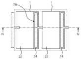
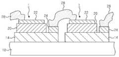
도 1은 상기 WO 2004/023568(Al)호에 따른 교류용 발광 다이오드를 설명하기 위한 부분적인 평면도이고, 도 2는 도 1의 절취선 IV-IV를 따라 취해진 단면도이다.1 is a partial plan view illustrating an AC light emitting diode according to WO 2004/023568 (Al), and FIG. 2 is a cross-sectional view taken along the line IV-IV of FIG. 1.
도 1 및 도 2를 참조하면, 기판(10) 상에 복수개의 발광셀들(1)이 형성된다. 또한, 상기 발광셀들(1) 상에 p-전극(22) 및 n-전극(24)이 형성된다. 에어브리지 배선(28)이 인접한 발광셀들의 p-전극(22)과 n-전극(24)을 전기적으로 연결하여, 복수개의 발광셀들(1)을 직렬 연결한다.1 and 2, a plurality of
각 발광셀은 n-GaN층(14), p-GaN층(20)을 포함한다. 도시하지는 않았지만, n-GaN층(14)과 p-GaN층(20) 사이에 InGaN 활성층이 개재될 수 있다. p-전극(22)은 상기 p-GaN층(20) 상에 형성되고, n-전극(24)은 상기 n-GaN층(14) 상에 형성된다. 한편, 에어브리지 배선(28)은 n-전극(24)과 p-전극(22)을 전기적으로 연결한다.Each light emitting cell includes an n-
상기 WO 2004/023568(Al)호에 따르면, LED들(발광셀들)이 사파이어 기판과 같은 절연성 기판 상에 2차원적으로 직렬연결되어 LED 어레이를 형성한다. 이러한 두개의 LED 어레이들이 상기 사파이어 기판 상에서 역병렬로 연결된다. 그 결과, AC 파워 서플라이에 의해 구동될 수 있는 단일칩 발광소자가 제공된다.According to WO 2004/023568 (Al), LEDs (light emitting cells) are two-dimensionally connected in series on an insulating substrate such as a sapphire substrate to form an LED array. These two LED arrays are connected in anti-parallel on the sapphire substrate. As a result, a single chip light emitting device that can be driven by an AC power supply is provided.
그러나, 도 1에 도시한 바와 같이, p-전극(22)과 n-전극(24)을 에어브리지 배선(28)으로 연결한 경우, 에어브리지 배선(28)을 통해 유입하는 순방향 전류가 p-전극(22)의 일부영역에 국부적으로 집중된다. 따라서, p-전극(22)의 일부영역에서 전류밀도가 증가하고, 그외 영역에서는 전류밀도가 상대적으로 낮게 된다. 이러한 국부적인 전류밀도의 증가는, 활성층의 발광영역을 제한할 뿐만 아니라, 과도한 전류밀도에 의해 p-전극(22)이 벗겨지는 현상(peeling)을 유발할 수 있다. 또한, 국부적인 전류밀도의 증가는 그 영역 내의 접합 온도를 증가시켜 발광효율을 감소시킬 수 있다. 이러한 문제점들은 고출력을 얻기 위해 전류를 증가시킬 경우, 더욱 현저해진다. 따라서, p-전극(22)내에서 국부적으로 전류가 집중되는 것을 방지하여, p-전극 전체적으로 고르게 전류를 분산시킬 수 있는 발광 다이오드가 요구된다.However, as shown in FIG. 1, when the p-
본 발명이 이루고자 하는 기술적 과제는, 발광셀 내에서 국부적으로 전류가 집중되는 것을 방지 또는 완화하고, 전류를 고르게 분산시킬 수 있는 교류용 발광 다이오드를 제공하는 데 있다.SUMMARY OF THE INVENTION The present invention has been made in an effort to provide an AC light emitting diode capable of preventing or alleviating local concentration of current in a light emitting cell and evenly distributing current.
상기 기술적 과제를 이루기 위하여, 본 발명의 일 태양은 단일 기판 상에 형성된 복수개의 발광셀들을 포함한다. 상기 발광셀들 각각은 제1 도전형 반도체층, 상기 제1 도전형 반도체층의 일영역 상에 위치하는 제2 도전형 반도체층 및 상기 제1 도전형 반도체층과 상기 제2 도전형 반도체층 사이에 개재된 활성층을 포함한다. 한편, 투명전극 구조체가 상기 각 발광셀 상에 위치한다. 상기 투명전극 구조체는 서로 분리된 적어도 두개의 부분들을 포함한다. 이에 더하여, 배선들이 상기 발광셀들 중 인접한 두개의 발광셀들을 각각 전기적으로 연결한다. 상기 배선들은 상기 인접한 발광셀들 중 하나의 발광셀 상에 위치하는 상기 투명전극 구조체의 적어도 두개의 부분들을 각각 다른 하나의 발광셀의 제1 도전형 반도체층에 전기적으로 연결한다.In order to achieve the above technical problem, an aspect of the present invention includes a plurality of light emitting cells formed on a single substrate. Each of the light emitting cells may include a first conductive semiconductor layer, a second conductive semiconductor layer positioned on one region of the first conductive semiconductor layer, and between the first conductive semiconductor layer and the second conductive semiconductor layer. It includes an active layer interposed therein. On the other hand, a transparent electrode structure is positioned on each light emitting cell. The transparent electrode structure includes at least two parts separated from each other. In addition, wirings electrically connect two adjacent light emitting cells, respectively. The wires electrically connect at least two portions of the transparent electrode structure positioned on one of the adjacent light emitting cells to the first conductive semiconductor layer of the other light emitting cell.
본 발명의 일 태양에 따르면, 투명전극 구조체의 서로 분리된 부분들과 인접한 제1 도전형 반도체층을 각각 연결함으로써, 상기 투명전극 구조체를 흐르는 전류를 분산시킬 수 있어 국부적인 전류밀도의 증가를 방지할 수 있다.According to an aspect of the present invention, by connecting the separated portions of the transparent electrode structure and the adjacent first conductive semiconductor layer, respectively, it is possible to disperse the current flowing through the transparent electrode structure to prevent a local increase in current density can do.
상기 투명전극 구조체의 적어도 두개의 부분들 각각은 상기 발광셀들 사이에서 전류가 흐르는 방향으로 기다란 형상을 가질 수 있다. 이에 따라, 상기 투명전극 구조체를 흐르는 전류가 각 부분들 내에서도 고르게 분산된다.Each of at least two portions of the transparent electrode structure may have an elongated shape in a direction in which current flows between the light emitting cells. Accordingly, the current flowing through the transparent electrode structure is evenly distributed within the respective parts.
한편, n형 전극이 상기 각 발광셀의 제1 도전형 반도체층의 다른 영역 상에 형성되고, p형 전극패드들이 상기 각 발광셀 상의 상기 투명전극 구조체의 적어도 두개의 부분들 각각에 형성되어 위치할 수 있다. 이때, 상기 배선들은 상기 n형 전극들과 상기 p형 전극패드들을 전기적으로 연결한다.Meanwhile, an n-type electrode is formed on another region of the first conductive semiconductor layer of each of the light emitting cells, and p-type electrode pads are formed on each of at least two portions of the transparent electrode structure on each of the light emitting cells. can do. In this case, the wires electrically connect the n-type electrodes and the p-type electrode pads.
상기 기술적 과제를 이루기 위하여, 본 발명의 다른 태양에 따른 교류용 발광 다이오드는 상기 투명전극 구조체를 변형한 것이다. 즉, 본 발명의 다른 태양에서, 투명전극 구조체는 상기 각 발광셀 상에 위치하되, 중심 부분과 상기 중심부분에서 양 옆으로 연장된 가지들을 포함한다. 이에 따라, 중심부분을 따라 흐르는 전류가 가지들의 끝단으로도 흐르게 되어 전류를 고르게 분산시킬 수 있다.In order to achieve the above technical problem, an AC light emitting diode according to another aspect of the present invention is a modification of the transparent electrode structure. That is, in another aspect of the present invention, the transparent electrode structure is positioned on each of the light emitting cells, and includes branches extending laterally from the central portion and the central portion. Accordingly, the current flowing along the center portion also flows to the ends of the branches, thereby evenly distributing the current.
한편, 배선들은 상기 발광셀들 중 인접한 두개의 발광셀들을 각각 전기적으로 연결하되, 상기 인접한 발광셀들 중 하나의 발광셀 상에 위치하는 상기 투명전극 구조체를 다른 하나의 발광셀의 제1 도전형 반도체층에 각각 전기적으로 연결한다.On the other hand, the wirings electrically connect two adjacent light emitting cells of the light emitting cells, respectively, and the first conductive type of the other light emitting cell is the transparent electrode structure positioned on one of the light emitting cells. It is electrically connected to each semiconductor layer.
이에 더하여, 상기 중심부분은 상기 발광셀들 사이에서 전류가 흐르는 방향으로 기다란 형상을 가질 수 있다. 또한, 상기 가지들은 상기 전류가 흐르는 방향에 수직하게 연장된다. 이에 따라, 상기 중심부분 내에서도 전류가 국부적으로 집중되는 것을 방지할 수 있다.In addition, the central portion may have an elongated shape in a direction in which current flows between the light emitting cells. In addition, the branches extend perpendicular to the direction in which the current flows. Accordingly, local concentration of current can be prevented even in the central portion.
또한, n형 전극이 상기 각 발광셀의 제1 도전형 반도체층의 다른 영역 상에 형성되고, p형 전극패드가 상기 각 발광셀 상의 상기 투명전극 구조체의 중심부분에 형성되어 위치할 수 있다. 이때, 상기 배선들 각각은 상기 n형 전극과 상기 p형 전극패드를 전기적으로 연결한다.In addition, an n-type electrode may be formed on another region of the first conductive semiconductor layer of each of the light emitting cells, and a p-type electrode pad may be formed and positioned at a central portion of the transparent electrode structure on each of the light emitting cells. In this case, each of the wires electrically connects the n-type electrode and the p-type electrode pad.
이하, 첨부한 도면들을 참조하여 본 발명의 실시예들을 상세히 설명하기로 한다. 다음에 소개되는 실시예들은 당업자에게 본 발명의 사상이 충분히 전달될 수 있도록 하기 위해 예로서 제공되는 것이다. 따라서, 본 발명은 이하 설명되는 실시예들에 한정되지 않고 다른 형태로 구체화될 수도 있다. 그리고, 도면들에 있어서, 구성요소의 폭, 길이, 두께 등은 편의를 위하여 과장되어 표현될 수 있다. 명세서 전체에 걸쳐서 동일한 참조번호들은 동일한 구성요소들을 나타낸다.Hereinafter, embodiments of the present invention will be described in detail with reference to the accompanying drawings. The following embodiments are provided as examples to ensure that the spirit of the present invention can be fully conveyed to those skilled in the art. Accordingly, the present invention is not limited to the embodiments described below and may be embodied in other forms. And, in the drawings, the width, length, thickness, etc. of the components may be exaggerated for convenience. Like numbers refer to like elements throughout.
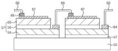
도 3은 본 발명의 일 실시예에 따른 교류용 발광 다이오드를 설명하기 위한 평면도이고, 도 4는 도 3의 절취선 I-I'를 따라 취해진 단면도이다.3 is a plan view illustrating an AC light emitting diode according to an exemplary embodiment of the present invention, and FIG. 4 is a cross-sectional view taken along the line II ′ of FIG. 3.
도 3 및 도 4를 참조하면, 단일 기판(50) 상에 복수개의 발광셀들(57)이 위치한다. 상기 기판(50)은 절연 또는 도전성 기판일 수 있다.3 and 4, a plurality of light emitting
상기 발광셀들(57) 각각은 제1 도전형 반도체층(54), 상기 제1 도전형 반도체층의 일영역 상에 위치하는 제2 도전형 반도체층(60) 및 상기 제1 도전형 반도체층과 제2 도전형 반도체층 사이에 개재된 활성층(56)을 포함한다. 여기서, 상기 제1 도전형 및 제2 도전형은 각각 n형 및 p형, 또는 p형 및 n형이다.Each of the light emitting
제1 도전형 반도체층(54), 활성층(56) 및 제2 도전형 반도체층(60)은 각각 질화갈륨 계열의 반도체 물질 즉, (B, Al, In, Ga)N으로 형성될 수 있다. 상기 활성층(56)은 요구되는 파장의 광 예컨대 자외선 또는 청색광을 방출하도록 조성 원소 및 조성비가 결정되며, 제1 도전형 반도체층(54) 및 제2 도전형 반도체층(60)은 상기 활성층(56)에 비해 밴드갭이 큰 물질로 형성된다.The first
상기 제1 도전형 반도체층(54) 및/또는 제2 도전형 반도체층(60)은, 도시한 바와 같이, 단일층으로 형성될 수 있으나, 다층 구조로 형성될 수도 있다. 또한, 활성층(56)은 단일 양자웰 또는 다중 양자웰 구조를 가질 수 있다.The first
한편, 상기 발광셀들(57)과 상기 기판(50) 사이에 버퍼층(52)이 개재될 수 있다. 버퍼층(52)은 기판(50)과 그 위에 형성될 제1 도전형 반도체층(54)의 격자부정합을 완화시키기 위해 채택된다.Meanwhile, a
상기 제1 도전형 반도체층(54)의 다른 영역, 즉 상기 제2 도전형 반도체층(60)이 형성된 영역에 인접하는 영역 상에 n형 전극(64)이 형성될 수 있다. 상기 n형 전극(64)은 제1 도전형 반도체층(64)에 오믹콘택된다. 한편, 제2 도전형 반도체층(29) 상에 투명전극 구조체(62)가 위치한다. 상기 투명전극 구조체(62)는 제2 도전형 반도체층(60)에 오믹콘택되며, 활성층(56)에서 방출된 광을 투과시킨다.The n-
상기 투명전극 구조체(62)는, 도 1에 도시한 바와 같이, 분리된 적어도 두개의 부분들을 포함한다. 상기 부분들 각각은, 발광셀들(57)을 동작시키기 위해 전류가 흐르는 방향, 즉 x 방향으로 기다란 형상을 갖는 것이 바람직하다.The
한편, 상기 각 부분들 상에 p형 전극패드(66)가 형성될 수 있다. 상기 p형 전극패드(66)는 상기 투명전극(62)을 관통하여 제2 도전형 반도체층(60)에 접촉할 수도 있으며, 이 경우, 상기 p형 전극패드(66)와 제2 도전형 반도체층(60)의 접촉저항이 큰 것이 바람직하다.Meanwhile, a p-
배선들(68)이, 도시한 바와 같이, 인접한 발광셀들의 제1 도전형 반도체층들(54)과 투명전극 구조체(62)를 전기적으로 연결한다. 상기 배선들은 전도성 물질, 예컨대 금속으로 형성된다. 배선들(68)은 상기 투명전극 구조체(62)의 적어도 두개의 부분들 각각을 인접한 발광셀의 제1 도전형 반도체층(54)에 전기적으로 연결한다. 한편, n형 전극들(64) 및 p형 전극패드들(66)이 형성된 경우, 상기 배선들(68)은 제1 도전형 반도체층(54) 상에 형성된 n형 전극(64)과 상기 투명전극 구조체(62)의 각 부분들에 형성된 p형 전극패드들(66)을 각각 전기적으로 연결할 수 있다.The
상기 배선들(68)은 발광셀들(57)을 직렬연결하여 발광셀들의 직렬 어레이를 형성한다. 이러한 어레이들이 복수개 형성될 수 있으며, 복수개의 어레이들이 서로 역병렬로 연결되어 교류전원에 연결될 수 있다. 또한, 발광셀들의 직렬 어레이에 연결된 브리지 정류기(도시하지 않음)가 형성될 수 있으며, 상기 브리지 정류기에 의해 상기 발광셀들이 교류전원하에서 구동될 수도 있다.The
본 실시예에 따르면, 투명전극 구조체(62)가 분리된 적어도 두개의 부분들을 포함하므로, 배선들(68)을 통해 투명전극 구조체(62)로 유입되는 전류는 분리된 각 부분들로 분산된다. 따라서, 종래의 단일 전극(도 1의 22)에 비해 일부영역에 전류가 집중되는 것을 방지할 수 있다. 또한, 상기 각 부분들이 전류가 흐르는 방향, 즉 x 방향으로 기다란 형상을 가지므로, 상기 각 부분들 내에서도 전류가 일부영역에 집중되는 것을 방지할 수 있다.According to the present embodiment, since the
도 5 내지 도 7은 본 발명의 일 실시예에 따른 교류용 발광 다이오드를 제조하는 방법을 설명하기 위한 단면도들이다.5 to 7 are cross-sectional views illustrating a method of manufacturing an AC LED according to an embodiment of the present invention.
도 5를 참조하면, 기판(50) 상에 제1 도전형 반도체층(54), 활성층(56) 및 제2 도전형 반도체층(60)을 형성한다. 또한, 상기 제1 도전형 반도체층(54)을 형성하기 전, 상기 기판(50) 상에 버퍼층(52)을 형성할 수 있다.Referring to FIG. 5, the first
상기 기판(50)은 사파이어(Al2O3), 탄화실리콘(SiC), 산화아연(ZnO), 실리콘(Si), 갈륨비소(GaAs), 갈륨인(GaP), 리튬-알루미나(LiAl2O3), 질화붕소(BN), 질화알루미늄(AlN) 또는 질화갈륨(GaN) 기판일 수 있으나, 이에 한정되는 것은 아니며, 기판(21) 상에 형성될 반도체층의 물질에 따라 다양하게 선택될 수 있다. 질화갈륨계 반도체층을 형성할 경우, 상기 기판(50)은 사파이어 또는 탄화실리콘(SiC) 기판이 주로 사용되고 있다.The
버퍼층(52)은 기판(50)과 그 위에 형성될 반도체층(54)의 격자부정합을 완화하기 위해 형성되며, 예컨대 질화갈륨(GaN) 또는 질화알루미늄(AlN)으로 형성될 수 있다. 상기 기판(50)이 전도성 기판인 경우, 상기 버퍼층(52)은 절연층 또는 반절연층으로 형성되는 것이 바람직하며, AlN 또는 반절연 GaN로 형성될 수 있다.The
제1 도전형 반도체층(54), 활성층(56) 및 제2 도전형 반도체층(60)은 각각 질화갈륨 계열의 반도체 물질 즉, (B, Al, In, Ga)N으로 형성될 수 있다. 상기 활성층(56)은 요구되는 파장의 광을 방출하도록 조성 원소 및 조성비가 결정되며, 제1 도전형 반도체층(54) 및 제2 도전형 반도체층(60)은 상기 활성층(56)에 비해 밴드갭이 큰 물질로 형성된다. 상기 제1 및 제2 도전형 반도체층(54, 60) 및 활성층(56)은 금속유기화학 기상증착(MOCVD), 분자선 성장(molecular beam epitaxy) 또는 수소화물 기상 성장(hydride vapor phase epitaxy; HVPE) 기술 등을 사용하여 단속 적으로 또는 연속적으로 성장될 수 있다.The first
여기서, 상기 제1 도전형 및 제2 도전형은 각각 n형 및 p형, 또는 p형 및 n형일 수 있다. 질화갈륨 계열의 화합물 반도체층에서, n형 반도체층은 불순물로 실리콘(Si)을 도핑하여 형성될 수 있으며, p형 반도체층은 불순물로 마그네슘(Mg)을 도핑하여 형성될 수 있다.Here, the first conductivity type and the second conductivity type may be n type and p type, or p type and n type, respectively. In the gallium nitride-based compound semiconductor layer, the n-type semiconductor layer may be formed by doping silicon (Si) as an impurity, and the p-type semiconductor layer may be formed by doping magnesium (Mg) as an impurity.
도 6을 참조하면, 상기 제2 도전형 반도체층(60), 활성층(56) 및 제1 도전형 반도체층(54)을 패터닝하여 서로 이격된 발광셀들(57)을 형성한다. 이때, 상기 버퍼층(52)도 함께 패터닝될 수 있다. 상기 제1 및 제2 도전형 반도체층들(54, 60) 및 활성층(56)은 사진 및 식각 공정을 사용하여 패터닝될 수 있다.Referring to FIG. 6, the second
한편, 제2 도전형 반도체층(60) 및 활성층(56)은, 도시한 바와 같이, 패터닝된 제1 도전형 반도체층(54)의 일영역 상에 위치하도록 패터닝된다. 이에 따라, 상기 패터닝된 제1 도전형 반도체층(54)의 일부 영역이 노출된다.Meanwhile, the second
도 7을 참조하면, 상기 패터닝된 제2 도전형 반도체층(60) 상에 투명전극 구조체(62)를 형성한다. 투명전극 구조체(62)는 리프트-오프(lift-off) 기술을 사용하여, 도 1에 도시한 바와 같이, 서로 분리된 적어도 두개의 부분들을 갖도록 형성될 수 있다. 이와 달리, 전자빔 증착(e-beam evaporation) 기술 등의 증착 기술을 사용하여 투명전극층을 형성한 후, 이를 사진 및 식각 공정을 사용하여 패터닝하여 적어도 두개의 부분들을 갖는 투명전극 구조체(62)를 형성할 수 있다. 상기 투명전극 구조체(62)는, 활성층(56)에서 방출된 광을 투과시킬 수 있는 전극 물질이면 특별히 한정되지 않으며, 예컨대 Ni/Au 또는 인디움-틴 산화막(ITO)으로 형성될 수 있다.Referring to FIG. 7, a
본 실시예에 있어서, 상기 투명전극 구조체(62)는 발광셀들(57)을 형성한 후에 형성되는 것으로 설명하지만, 이에 한정되는 것은 아니며, 발광셀들(57)을 분리하기 전에 형성될 수 있다. 특히, 전자빔 증착기술을 사용하여 투명전극층을 증착할 경우, 제2 도전형 반도체층(60)을 성장시킨 후, 상기 발광셀들(57)을 분리하기 전, 투명전극층을 형성하는 것이 바람직하다. 이후, 배선(68)을 형성하기 전, 소정 단계에서 투명전극층이 패터닝되어 투명전극 구조체(62)가 형성된다.In the present exemplary embodiment, the
상기 투명전극 구조체(62)의 일부 영역 상에 p형 전극패드(66)가 형성될 수 있다. p형 전극패드(66)는 리프트-오프 기술을 사용하여 형성될 수 있다. 한편, 상기 p형 전극패드(66)를 형성하기 전, 상기 투면전극 구조체(62)를 패터닝하여 상기 제2 도전형 반도체층(60)을 노출시키는 개구부(도시하지 않음)를 형성할 수 있다. 그 후, 상기 개구부 및 그 주변에 p형 전극패드(62)를 형성한다. 그 결과, 상기 개구부를 통해 p형 전극패드(66)가 제2 도전형 반도체층(60)에 접촉될 수 있다.The p-
한편, 제1 도전형 반도체층(54)의 다른 영역 상에 n형 전극(64)가 형성될 수 있다. 상기 n형 전극(64) 또한 리프트 오프 기술을 사용하여 형성될 수 있으며, 상기 p형 전극패드(66)와 동시에 형성될 수도 있다. 상기 p형 전극패드(66) 및/또는 n형 전극(64)은 Ti/Au로 형성될 수 있다.Meanwhile, the n-
이어서, 인접한 발광셀들(57)을 전기적으로 연결하는 배선들(68)을 형성한다. 상기 배선들은 상기 n형 전극(64)과 p형 전극패드들(66)을 연결할 수 있으며, 이에 따라 도 3 및 도 4를 참조하여 설명한 발광 다이오드가 형성된다.Subsequently,
배선들(68)은, 에어브리지(air-bridge) 공정을 사용하여 형성될 수 있으며, 도 4는 에어브리지 공정을 사용하여 형성된 배선들을 도시하고 있다. 상기 배선들(68)은 또한 스텝커버(step-cover) 공정을 사용하여 형성될 수도 있다.The
우선, 상기 에어브리지(air bridge) 공정의 일예에 대해 간단하게 설명한다. 도 7에 도시한 바와 같이, n형 전극들(64) 및 p형 전극패드들(66)이 형성된 기판(50) 상에 감광막을 형성한 후, 노광기술을 사용하여 n형 전극들(64) 및 p형 전극패드들(66)을 노출시키는 개구부들을 갖는 제1 감광막 패턴을 형성한다. 그 후, 전자빔 증착(e-beam evaporation) 기술등을 사용하여 금속물질층을 얇게 형성한다. 상기 금속물질층은 개구부들 및 감광막 패턴 상부 전면에 형성된다. 이어서, 상기 감광막 패턴 상에, 연결하고자 하는 인접한 발광셀들 사이의 영역들 및 상기 개구부들 내의 상기 금속물질층을 노출시키는 제2 감광막 패턴을 형성한다. 그 후, 금 등을 도금기술을 사용하여 형성한 후, 상기 제1 및 제2 감광막 패턴들을 모두 제거한다. 그 결과, 인접한 발광셀들의 n형 전극(64)과 p형 전극패드들(66)을 각각 연결하는 배선들(68)은 남고, 다른 금속물질층 및 감광막 패턴들은 모두 제거되어, 상기 배선들(68)이, 도시한 바와 같이, 브리지 형태로 상기 발광셀들(57)을 전기적으로 연결한다.First, an example of the air bridge process will be briefly described. As shown in FIG. 7, after the photosensitive film is formed on the
한편, 스텝커버 공정은, 도 7에 도시한 바와 같이, n형 전극들(64) 및 p형 전극패드들(66)을 갖는 기판 상에 절연층을 형성하는 것을 포함한다. 그후, 사진 및 식각 기술을 사용하여 상기 절연층을 패터닝하여 n형 전극들(64) 및 p형 전극패드들(66)을 노출시키는 개구부들을 형성한다. 이어서, 전자빔 증착기술 등을 사용 하여 상기 개구부를 채우고 상기 절연층 상부를 덮는 금속층을 형성한다. 그 후, 상기 금속층을 사진 및 식각 기술을 사용하여 패터닝하여 서로 인접한 발광셀들(57)을 연결하는 배선들(58)을 형성한다. 이러한, 스텝커버 공정은 다양한 변형예가 가능하다. 스텝커버 공정을 사용하면, 배선들(68)이 절연층에 의해 지지되므로 신뢰성을 증가시킬 수 있다.Meanwhile, the step cover process includes forming an insulating layer on a substrate having n-
상기 배선들(68)은, 도 3에 도시한 바와 같이, n형 전극들(64) 상에서 서로 분리되도록 형성될 수 있으나, n형 전극들(64) 상에서 서로 연결될 수도 있다.The
도 8은 본 발명의 다른 실시예에 따른 교류용 발광 다이오드를 설명하기 위한 평면도이다.8 is a plan view illustrating an AC LED according to another embodiment of the present invention.
본 실시예에 따른 교류용 발광 다이오드는 도 3을 참조하여 설명한 교류용 발광 다이오드와 대체로 동일한 구성요소들을 갖는다. 다만, 본 실시예에 따른 교류용 발광 다이오드는 투명전극 구조체(72)가 세 부분으로 분리되어 있는 것을 나타내고 있으며, n형 전극들(64) 상에서 배선들(78)이 서로 연결되어 있는 것을 나타내고 있다.The AC light emitting diode according to the present embodiment generally has the same components as the AC light emitting diode described with reference to FIG. 3. However, the AC LED according to the present embodiment shows that the
상기 투명전극 구조체(72), x 방향을 따라 기다란 형상을 갖는 부분들로 분리될 수 있으며, 상기 부분들은, 국부적인 전류의 집중을 방지하기 위해, 다양한 수로 분리될 수 있다.The
한편, 배선들(78)이 n형 전극들(64) 상에서 서로 연결될 경우, 배선들(68)의 접착력이 개선될 수 있으나, 서로 분리될 수도 있다.Meanwhile, when the
도 9는 본 발명의 또 다른 실시예에 따른 교류용 발광 다이오드를 설명하기 위한 평면도이다.9 is a plan view illustrating an AC light emitting diode according to still another embodiment of the present invention.
도 9를 참조하면, 본 실시예에 따른 교류용 발광 다이오드는 도 3을 참조하여 설명한 교류용 발광 다이오드와 대체로 동일한 구성요소들을 갖는다. 다만, 투명전극 구조체(82)가 도 3의 투명전극 구조체(62)와 차이가 있으며, 이에 따라 배선들(88)이 도 3의 배선들(68)과 차이가 있다. 이하에서, 상기 차이점들에 대해 설명한다.Referring to FIG. 9, the AC light emitting diode according to the present embodiment generally has the same components as the AC light emitting diode described with reference to FIG. 3. However, the
상기 투명전극 구조체(82)는 중심부분(82a)과 상기 중심부분(82b)에서 양옆으로 연장된 가지들(82b)을 포함한다. 중심부분(82a)은 발광셀들(57) 사이에서 전류가 흐르는 방향, 즉 x 방향으로 기다란 형상을 가질 수 있다. 또한, 가지들(82b)은 전류가 흐르는 방향에 수직한 방향, 즉 y 방향으로 연장된다.The
한편, 배선들(88)이 인접한 발광셀들(57)을 전기적으로 연결한다. 상기 배선들(88)은 n형 전극(64)과 투명전극 구조체(82)를 전기적으로 연결하며, 특히 상기 투명전극 구조체(82)의 중심부분(82a)과 n형 전극(64)을 연결할 수 있다.On the other hand, the
이에 따라, 상기 중심부분(82a) 내에서 전류가 일부 영역에 집중되는 것을 방지할 수 있으며, 가지들(82b)을 통해 발광셀 영역에 전류를 분산시킬 수 있다.Accordingly, it is possible to prevent the current from being concentrated in some areas in the
본 발명의 실시예들에 따르면, 발광셀 내에서 국부적으로 전류가 집중되는 것을 방지 또는 완화하고, 전류를 고르게 분산시킬 수 있는 교류용 발광 다이오드를 제공할 수 있다. 이에 따라, 국부적으로 집중되는 과도한 전류에 의해 p-전극(22)이 벗겨지는 현상(peeling)을 방지할 수 있으며, 발광셀(57)의 전 영역에 고르 게 전류를 분산시키어 발광효율이 개선된다. 또한, 전류를 고르게 분산시킬 수 있으므로, 종래기술에 비해 전류를 더욱 증가시키어 고출력을 얻을 수 있는 교류용 발광 다이오드를 제공할 수 있다.According to embodiments of the present invention, it is possible to provide an AC light emitting diode capable of preventing or alleviating local concentration of current in the light emitting cell and evenly distributing the current. Accordingly, the p-
Claims (6)
Translated fromKoreanPriority Applications (8)
| Application Number | Priority Date | Filing Date | Title |
|---|---|---|---|
| KR1020050124256AKR100652864B1 (en) | 2005-12-16 | 2005-12-16 | Light emitting diode for alternating current with improved transparent electrode structure |
| US12/088,999US7994523B2 (en) | 2005-12-16 | 2006-11-28 | AC light emitting diode having improved transparent electrode structure |
| DE112006004103.7TDE112006004103B4 (en) | 2005-12-16 | 2006-11-28 | AC-powered light emitting diode array |
| DE112006002883TDE112006002883B4 (en) | 2005-12-16 | 2006-11-28 | AC powered light emitting diode array |
| CNB2006800415821ACN100552995C (en) | 2005-12-16 | 2006-11-28 | AC Light Emitting Diodes with Improved Transparent Electrode Structure |
| JP2008545477AJP5073675B2 (en) | 2005-12-16 | 2006-11-28 | AC driven light emitting diode with improved transparent electrode structure |
| PCT/KR2006/005050WO2007083884A1 (en) | 2005-12-16 | 2006-11-28 | Ac light emitting diode having improved transparent electrode structure |
| TW095146587ATWI367572B (en) | 2005-12-16 | 2006-12-13 | Ac light emitting diode having improved transparent electrode structure |
Applications Claiming Priority (1)
| Application Number | Priority Date | Filing Date | Title |
|---|---|---|---|
| KR1020050124256AKR100652864B1 (en) | 2005-12-16 | 2005-12-16 | Light emitting diode for alternating current with improved transparent electrode structure |
Publications (1)
| Publication Number | Publication Date |
|---|---|
| KR100652864B1true KR100652864B1 (en) | 2006-12-04 |
Family
ID=37731748
Family Applications (1)
| Application Number | Title | Priority Date | Filing Date |
|---|---|---|---|
| KR1020050124256AExpired - Fee RelatedKR100652864B1 (en) | 2005-12-16 | 2005-12-16 | Light emitting diode for alternating current with improved transparent electrode structure |
Country Status (7)
| Country | Link |
|---|---|
| US (1) | US7994523B2 (en) |
| JP (1) | JP5073675B2 (en) |
| KR (1) | KR100652864B1 (en) |
| CN (1) | CN100552995C (en) |
| DE (2) | DE112006002883B4 (en) |
| TW (1) | TWI367572B (en) |
| WO (1) | WO2007083884A1 (en) |
Cited By (7)
| Publication number | Priority date | Publication date | Assignee | Title |
|---|---|---|---|---|
| KR101040140B1 (en) | 2010-11-03 | 2011-06-09 | (주)더리즈 | Semiconductor light emitting device array and manufacturing method thereof |
| KR101138975B1 (en)* | 2009-09-15 | 2012-04-25 | 서울옵토디바이스주식회사 | Ac light emitting diode having full-wave lihgt emitting cell and half-wave light emitting cell |
| KR101396586B1 (en)* | 2007-09-14 | 2014-05-21 | 서울반도체 주식회사 | Hybrid light emitting device |
| KR101803014B1 (en) | 2011-08-24 | 2017-12-01 | 서울바이오시스 주식회사 | Light emitting diode |
| KR101926360B1 (en)* | 2012-03-06 | 2018-12-07 | 삼성전자주식회사 | Semiconductor light emitting device having a multi-cell array |
| CN110783437A (en)* | 2018-07-24 | 2020-02-11 | 首尔伟傲世有限公司 | Light emitting diode having zinc oxide layer and method for manufacturing the same |
| CN115552610A (en)* | 2020-05-13 | 2022-12-30 | 三星显示有限公司 | Display device |
Families Citing this family (20)
| Publication number | Priority date | Publication date | Assignee | Title |
|---|---|---|---|---|
| US8461613B2 (en) | 2008-05-27 | 2013-06-11 | Interlight Optotech Corporation | Light emitting device |
| JP2010205910A (en)* | 2009-03-03 | 2010-09-16 | Toshiba Corp | Semiconductor light emitting device |
| US20110203656A1 (en)* | 2010-02-24 | 2011-08-25 | Iowa State University Research Foundation, Inc. | Nanoscale High-Aspect-Ratio Metallic Structure and Method of Manufacturing Same |
| JP5195798B2 (en)* | 2010-03-23 | 2013-05-15 | 豊田合成株式会社 | Manufacturing method of semiconductor light emitting device |
| WO2011126248A2 (en)* | 2010-04-06 | 2011-10-13 | Seoul Opto Device Co., Ltd. | Light emitting diode and method of fabricating the same |
| TWI446527B (en)* | 2010-07-02 | 2014-07-21 | Epistar Corp | Optoelectronic component |
| CN102446948B (en)* | 2010-10-12 | 2014-07-30 | 晶元光电股份有限公司 | Light emitting element |
| CN102097562A (en)* | 2010-12-14 | 2011-06-15 | 金木子 | Alternating current surface mounted type vertical structure semiconductor light-emitting diode |
| JP5772213B2 (en)* | 2011-05-20 | 2015-09-02 | サンケン電気株式会社 | Light emitting element |
| CN102903818A (en)* | 2011-07-27 | 2013-01-30 | 南通同方半导体有限公司 | High-power GaN (gallium nitride)-based light emitting diode structure and manufacturing method thereof |
| TWI549278B (en)* | 2012-03-12 | 2016-09-11 | 晶元光電股份有限公司 | Light-emitting diode component |
| CN103367384B (en)* | 2012-03-30 | 2018-04-03 | 晶元光电股份有限公司 | LED components |
| CN108598102B (en)* | 2012-08-15 | 2021-11-05 | 晶元光电股份有限公司 | Light emitting device |
| US9171826B2 (en)* | 2012-09-04 | 2015-10-27 | Micron Technology, Inc. | High voltage solid-state transducers and solid-state transducer arrays having electrical cross-connections and associated systems and methods |
| WO2016129873A2 (en)* | 2015-02-13 | 2016-08-18 | 서울바이오시스 주식회사 | Light-emitting element and light-emitting diode |
| KR102357188B1 (en)* | 2015-07-21 | 2022-01-28 | 쑤저우 레킨 세미컨덕터 컴퍼니 리미티드 | Light emitting device |
| TWI700683B (en) | 2018-12-06 | 2020-08-01 | 友達光電股份有限公司 | Pixel structure |
| JP7014973B2 (en)* | 2019-08-28 | 2022-02-02 | 日亜化学工業株式会社 | Luminescent device |
| US20230007967A1 (en)* | 2021-07-12 | 2023-01-12 | Xiamen San'an Optoelectronics Co., Ltd. | Light emitting diode device |
| CN114256390B (en)* | 2021-12-13 | 2024-07-02 | 广东省科学院半导体研究所 | LED array chip and manufacturing method thereof |
Citations (5)
| Publication number | Priority date | Publication date | Assignee | Title |
|---|---|---|---|---|
| JPH09107125A (en)* | 1996-09-17 | 1997-04-22 | Nichia Chem Ind Ltd | Gallium nitride based compound semiconductor light emitting device |
| KR20020084710A (en)* | 2001-05-02 | 2002-11-11 | 광주과학기술원 | GaN-Based Light Emitting Diode and Fabrication Method thereof |
| JP2004014899A (en) | 2002-06-10 | 2004-01-15 | Para Light Electronics Co Ltd | Series connection of light emitting diode chip |
| JP2004048067A (en) | 2003-10-14 | 2004-02-12 | Sanyo Electric Co Ltd | Light emitting component and method for manufacturing the same |
| JP2004079867A (en) | 2002-08-21 | 2004-03-11 | Shiro Sakai | Manufacturing method of gallium nitride base compound semiconductor device, and light emitting device |
Family Cites Families (15)
| Publication number | Priority date | Publication date | Assignee | Title |
|---|---|---|---|---|
| US5223723A (en)* | 1990-10-19 | 1993-06-29 | At&T Bell Laboratories | Light emitting device |
| DE19517697A1 (en)* | 1995-05-13 | 1996-11-14 | Telefunken Microelectron | Orange to green light emitting semiconductor LED |
| JPH118442A (en)* | 1996-10-07 | 1999-01-12 | Canon Inc | Optical semiconductor device, optical communication system and method using the same |
| JP3934730B2 (en)* | 1997-03-28 | 2007-06-20 | ローム株式会社 | Semiconductor light emitting device |
| JP2000068555A (en)* | 1998-08-19 | 2000-03-03 | Hitachi Ltd | Lighting system |
| US6307218B1 (en)* | 1998-11-20 | 2001-10-23 | Lumileds Lighting, U.S., Llc | Electrode structures for light emitting devices |
| JP2000277806A (en)* | 1999-03-26 | 2000-10-06 | Oki Electric Ind Co Ltd | Light emitting diode array |
| TW583774B (en) | 1999-12-01 | 2004-04-11 | Cree Inc | Scalable LED with improved current spreading structures |
| US6885035B2 (en) | 1999-12-22 | 2005-04-26 | Lumileds Lighting U.S., Llc | Multi-chip semiconductor LED assembly |
| JP4075321B2 (en)* | 2001-04-24 | 2008-04-16 | 日亜化学工業株式会社 | Integrated nitride semiconductor light emitting device |
| ATE500616T1 (en)* | 2002-08-29 | 2011-03-15 | Seoul Semiconductor Co Ltd | LIGHT EMITTING COMPONENT WITH LIGHT EMITTING DIODES |
| TWI224876B (en) | 2003-12-23 | 2004-12-01 | Uni Light Technology Inc | Method for forming an LED device with a metallic substrate |
| US7615798B2 (en)* | 2004-03-29 | 2009-11-10 | Nichia Corporation | Semiconductor light emitting device having an electrode made of a conductive oxide |
| DE102004021175B4 (en)* | 2004-04-30 | 2023-06-29 | OSRAM Opto Semiconductors Gesellschaft mit beschränkter Haftung | Semiconductor chips for optoelectronics and methods for their manufacture |
| TW200501464A (en) | 2004-08-31 | 2005-01-01 | Ind Tech Res Inst | LED chip structure with AC loop |
- 2005
- 2005-12-16KRKR1020050124256Apatent/KR100652864B1/ennot_activeExpired - Fee Related
- 2006
- 2006-11-28DEDE112006002883Tpatent/DE112006002883B4/ennot_activeExpired - Fee Related
- 2006-11-28CNCNB2006800415821Apatent/CN100552995C/ennot_activeExpired - Fee Related
- 2006-11-28USUS12/088,999patent/US7994523B2/ennot_activeExpired - Fee Related
- 2006-11-28DEDE112006004103.7Tpatent/DE112006004103B4/ennot_activeExpired - Fee Related
- 2006-11-28WOPCT/KR2006/005050patent/WO2007083884A1/enactiveApplication Filing
- 2006-11-28JPJP2008545477Apatent/JP5073675B2/ennot_activeExpired - Fee Related
- 2006-12-13TWTW095146587Apatent/TWI367572B/ennot_activeIP Right Cessation
Patent Citations (5)
| Publication number | Priority date | Publication date | Assignee | Title |
|---|---|---|---|---|
| JPH09107125A (en)* | 1996-09-17 | 1997-04-22 | Nichia Chem Ind Ltd | Gallium nitride based compound semiconductor light emitting device |
| KR20020084710A (en)* | 2001-05-02 | 2002-11-11 | 광주과학기술원 | GaN-Based Light Emitting Diode and Fabrication Method thereof |
| JP2004014899A (en) | 2002-06-10 | 2004-01-15 | Para Light Electronics Co Ltd | Series connection of light emitting diode chip |
| JP2004079867A (en) | 2002-08-21 | 2004-03-11 | Shiro Sakai | Manufacturing method of gallium nitride base compound semiconductor device, and light emitting device |
| JP2004048067A (en) | 2003-10-14 | 2004-02-12 | Sanyo Electric Co Ltd | Light emitting component and method for manufacturing the same |
Cited By (7)
| Publication number | Priority date | Publication date | Assignee | Title |
|---|---|---|---|---|
| KR101396586B1 (en)* | 2007-09-14 | 2014-05-21 | 서울반도체 주식회사 | Hybrid light emitting device |
| KR101138975B1 (en)* | 2009-09-15 | 2012-04-25 | 서울옵토디바이스주식회사 | Ac light emitting diode having full-wave lihgt emitting cell and half-wave light emitting cell |
| KR101040140B1 (en) | 2010-11-03 | 2011-06-09 | (주)더리즈 | Semiconductor light emitting device array and manufacturing method thereof |
| KR101803014B1 (en) | 2011-08-24 | 2017-12-01 | 서울바이오시스 주식회사 | Light emitting diode |
| KR101926360B1 (en)* | 2012-03-06 | 2018-12-07 | 삼성전자주식회사 | Semiconductor light emitting device having a multi-cell array |
| CN110783437A (en)* | 2018-07-24 | 2020-02-11 | 首尔伟傲世有限公司 | Light emitting diode having zinc oxide layer and method for manufacturing the same |
| CN115552610A (en)* | 2020-05-13 | 2022-12-30 | 三星显示有限公司 | Display device |
Also Published As
| Publication number | Publication date |
|---|---|
| WO2007083884A1 (en) | 2007-07-26 |
| US7994523B2 (en) | 2011-08-09 |
| TWI367572B (en) | 2012-07-01 |
| CN101305475A (en) | 2008-11-12 |
| DE112006002883B4 (en) | 2010-09-09 |
| TW200725952A (en) | 2007-07-01 |
| DE112006004103B4 (en) | 2021-06-02 |
| JP5073675B2 (en) | 2012-11-14 |
| JP2009519604A (en) | 2009-05-14 |
| US20080217629A1 (en) | 2008-09-11 |
| CN100552995C (en) | 2009-10-21 |
| DE112006002883T5 (en) | 2008-09-18 |
Similar Documents
| Publication | Publication Date | Title |
|---|---|---|
| KR100652864B1 (en) | Light emitting diode for alternating current with improved transparent electrode structure | |
| KR100690323B1 (en) | Light emitting diode for alternating current having wirings and method for manufacturing same | |
| US7723736B2 (en) | Light emitting device having a plurality of light emitting cells and package mounting the same | |
| KR100838197B1 (en) | Light Emitting Diodes with Improved Current Dissipation Performance | |
| US6547249B2 (en) | Monolithic series/parallel led arrays formed on highly resistive substrates | |
| US9209223B2 (en) | Light emitting device and method of manufacturing the same | |
| US7015512B2 (en) | High power flip chip LED | |
| CN204167323U (en) | Light-emitting diode | |
| KR101423723B1 (en) | Light emitting diode package | |
| EP1905103B1 (en) | Method of fabricating a light emitting diode having a thermal conductive substrate | |
| CN101807593B (en) | Light emitting device and manufacture method thereof | |
| US11430934B2 (en) | Light-emitting diode device | |
| US20050225973A1 (en) | LED with series-connected monolithically integrated mesas | |
| CN101515595A (en) | Package mounting light emitting device | |
| US11404474B2 (en) | Light-emitting device and manufacturing method thereof | |
| US20210119084A1 (en) | Optoelectronic device | |
| KR100757800B1 (en) | Light emitting diode for alternating current having an insulating protective film and a method of manufacturing the same | |
| KR20140117791A (en) | Light emitting diode and method of fabricating the same | |
| KR100765452B1 (en) | Light emitting diodes and manufacturing method | |
| JP2012243972A (en) | Light emitting element | |
| KR20080044439A (en) | A light emitting device in which a plurality of cells are combined and a method of manufacturing the same | |
| KR20150020096A (en) | Light emitting diode and method of fabricating the same | |
| KR100599014B1 (en) | Light emitting device having a hetero semiconductor repeating layer and a method of manufacturing the same |
Legal Events
| Date | Code | Title | Description |
|---|---|---|---|
| A201 | Request for examination | ||
| PA0109 | Patent application | St.27 status event code:A-0-1-A10-A12-nap-PA0109 | |
| PA0201 | Request for examination | St.27 status event code:A-1-2-D10-D11-exm-PA0201 | |
| D13-X000 | Search requested | St.27 status event code:A-1-2-D10-D13-srh-X000 | |
| D14-X000 | Search report completed | St.27 status event code:A-1-2-D10-D14-srh-X000 | |
| E701 | Decision to grant or registration of patent right | ||
| PE0701 | Decision of registration | St.27 status event code:A-1-2-D10-D22-exm-PE0701 | |
| GRNT | Written decision to grant | ||
| PR0701 | Registration of establishment | St.27 status event code:A-2-4-F10-F11-exm-PR0701 | |
| PR1002 | Payment of registration fee | St.27 status event code:A-2-2-U10-U11-oth-PR1002 Fee payment year number:1 | |
| PG1601 | Publication of registration | St.27 status event code:A-4-4-Q10-Q13-nap-PG1601 | |
| P22-X000 | Classification modified | St.27 status event code:A-4-4-P10-P22-nap-X000 | |
| PR1001 | Payment of annual fee | St.27 status event code:A-4-4-U10-U11-oth-PR1001 Fee payment year number:4 | |
| PR1001 | Payment of annual fee | St.27 status event code:A-4-4-U10-U11-oth-PR1001 Fee payment year number:5 | |
| PR1001 | Payment of annual fee | St.27 status event code:A-4-4-U10-U11-oth-PR1001 Fee payment year number:6 | |
| FPAY | Annual fee payment | Payment date:20120917 Year of fee payment:7 | |
| PR1001 | Payment of annual fee | St.27 status event code:A-4-4-U10-U11-oth-PR1001 Fee payment year number:7 | |
| FPAY | Annual fee payment | Payment date:20130911 Year of fee payment:8 | |
| PR1001 | Payment of annual fee | St.27 status event code:A-4-4-U10-U11-oth-PR1001 Fee payment year number:8 | |
| R18-X000 | Changes to party contact information recorded | St.27 status event code:A-5-5-R10-R18-oth-X000 | |
| R18-X000 | Changes to party contact information recorded | St.27 status event code:A-5-5-R10-R18-oth-X000 | |
| PN2301 | Change of applicant | St.27 status event code:A-5-5-R10-R13-asn-PN2301 St.27 status event code:A-5-5-R10-R11-asn-PN2301 | |
| FPAY | Annual fee payment | Payment date:20141001 Year of fee payment:9 | |
| PR1001 | Payment of annual fee | St.27 status event code:A-4-4-U10-U11-oth-PR1001 Fee payment year number:9 | |
| FPAY | Annual fee payment | Payment date:20150924 Year of fee payment:10 | |
| PR1001 | Payment of annual fee | St.27 status event code:A-4-4-U10-U11-oth-PR1001 Fee payment year number:10 | |
| FPAY | Annual fee payment | Payment date:20160907 Year of fee payment:11 | |
| PR1001 | Payment of annual fee | St.27 status event code:A-4-4-U10-U11-oth-PR1001 Fee payment year number:11 | |
| FPAY | Annual fee payment | Payment date:20170911 Year of fee payment:12 | |
| PR1001 | Payment of annual fee | St.27 status event code:A-4-4-U10-U11-oth-PR1001 Fee payment year number:12 | |
| PR1001 | Payment of annual fee | St.27 status event code:A-4-4-U10-U11-oth-PR1001 Fee payment year number:13 | |
| FPAY | Annual fee payment | Payment date:20191001 Year of fee payment:14 | |
| PR1001 | Payment of annual fee | St.27 status event code:A-4-4-U10-U11-oth-PR1001 Fee payment year number:14 | |
| PC1903 | Unpaid annual fee | St.27 status event code:A-4-4-U10-U13-oth-PC1903 Not in force date:20201125 Payment event data comment text:Termination Category : DEFAULT_OF_REGISTRATION_FEE | |
| PC1903 | Unpaid annual fee | St.27 status event code:N-4-6-H10-H13-oth-PC1903 Ip right cessation event data comment text:Termination Category : DEFAULT_OF_REGISTRATION_FEE Not in force date:20201125 | |
| P22-X000 | Classification modified | St.27 status event code:A-4-4-P10-P22-nap-X000 |