KR100652378B1 - Antimony precursor and manufacturing method of phase change memory device using same - Google Patents
Antimony precursor and manufacturing method of phase change memory device using sameDownload PDFInfo
- Publication number
- KR100652378B1 KR100652378B1KR1020040071868AKR20040071868AKR100652378B1KR 100652378 B1KR100652378 B1KR 100652378B1KR 1020040071868 AKR1020040071868 AKR 1020040071868AKR 20040071868 AKR20040071868 AKR 20040071868AKR 100652378 B1KR100652378 B1KR 100652378B1
- Authority
- KR
- South Korea
- Prior art keywords
- phase change
- antimony
- precursor
- memory device
- impurity region
- Prior art date
- Legal status (The legal status is an assumption and is not a legal conclusion. Google has not performed a legal analysis and makes no representation as to the accuracy of the status listed.)
- Expired - Fee Related
Links
Images


Classifications
- C—CHEMISTRY; METALLURGY
- C07—ORGANIC CHEMISTRY
- C07F—ACYCLIC, CARBOCYCLIC OR HETEROCYCLIC COMPOUNDS CONTAINING ELEMENTS OTHER THAN CARBON, HYDROGEN, HALOGEN, OXYGEN, NITROGEN, SULFUR, SELENIUM OR TELLURIUM
- C07F9/00—Compounds containing elements of Groups 5 or 15 of the Periodic Table
- C07F9/90—Antimony compounds
- C07F9/902—Compounds without antimony-carbon linkages
- C—CHEMISTRY; METALLURGY
- C23—COATING METALLIC MATERIAL; COATING MATERIAL WITH METALLIC MATERIAL; CHEMICAL SURFACE TREATMENT; DIFFUSION TREATMENT OF METALLIC MATERIAL; COATING BY VACUUM EVAPORATION, BY SPUTTERING, BY ION IMPLANTATION OR BY CHEMICAL VAPOUR DEPOSITION, IN GENERAL; INHIBITING CORROSION OF METALLIC MATERIAL OR INCRUSTATION IN GENERAL
- C23C—COATING METALLIC MATERIAL; COATING MATERIAL WITH METALLIC MATERIAL; SURFACE TREATMENT OF METALLIC MATERIAL BY DIFFUSION INTO THE SURFACE, BY CHEMICAL CONVERSION OR SUBSTITUTION; COATING BY VACUUM EVAPORATION, BY SPUTTERING, BY ION IMPLANTATION OR BY CHEMICAL VAPOUR DEPOSITION, IN GENERAL
- C23C16/00—Chemical coating by decomposition of gaseous compounds, without leaving reaction products of surface material in the coating, i.e. chemical vapour deposition [CVD] processes
- C23C16/06—Chemical coating by decomposition of gaseous compounds, without leaving reaction products of surface material in the coating, i.e. chemical vapour deposition [CVD] processes characterised by the deposition of metallic material
- C23C16/18—Chemical coating by decomposition of gaseous compounds, without leaving reaction products of surface material in the coating, i.e. chemical vapour deposition [CVD] processes characterised by the deposition of metallic material from metallo-organic compounds
- C—CHEMISTRY; METALLURGY
- C23—COATING METALLIC MATERIAL; COATING MATERIAL WITH METALLIC MATERIAL; CHEMICAL SURFACE TREATMENT; DIFFUSION TREATMENT OF METALLIC MATERIAL; COATING BY VACUUM EVAPORATION, BY SPUTTERING, BY ION IMPLANTATION OR BY CHEMICAL VAPOUR DEPOSITION, IN GENERAL; INHIBITING CORROSION OF METALLIC MATERIAL OR INCRUSTATION IN GENERAL
- C23C—COATING METALLIC MATERIAL; COATING MATERIAL WITH METALLIC MATERIAL; SURFACE TREATMENT OF METALLIC MATERIAL BY DIFFUSION INTO THE SURFACE, BY CHEMICAL CONVERSION OR SUBSTITUTION; COATING BY VACUUM EVAPORATION, BY SPUTTERING, BY ION IMPLANTATION OR BY CHEMICAL VAPOUR DEPOSITION, IN GENERAL
- C23C16/00—Chemical coating by decomposition of gaseous compounds, without leaving reaction products of surface material in the coating, i.e. chemical vapour deposition [CVD] processes
- C23C16/44—Chemical coating by decomposition of gaseous compounds, without leaving reaction products of surface material in the coating, i.e. chemical vapour deposition [CVD] processes characterised by the method of coating
- C23C16/455—Chemical coating by decomposition of gaseous compounds, without leaving reaction products of surface material in the coating, i.e. chemical vapour deposition [CVD] processes characterised by the method of coating characterised by the method used for introducing gases into reaction chamber or for modifying gas flows in reaction chamber
- C23C16/45523—Pulsed gas flow or change of composition over time
- C23C16/45525—Atomic layer deposition [ALD]
- C23C16/45527—Atomic layer deposition [ALD] characterized by the ALD cycle, e.g. different flows or temperatures during half-reactions, unusual pulsing sequence, use of precursor mixtures or auxiliary reactants or activations
- C23C16/45531—Atomic layer deposition [ALD] characterized by the ALD cycle, e.g. different flows or temperatures during half-reactions, unusual pulsing sequence, use of precursor mixtures or auxiliary reactants or activations specially adapted for making ternary or higher compositions
- H—ELECTRICITY
- H10—SEMICONDUCTOR DEVICES; ELECTRIC SOLID-STATE DEVICES NOT OTHERWISE PROVIDED FOR
- H10B—ELECTRONIC MEMORY DEVICES
- H10B63/00—Resistance change memory devices, e.g. resistive RAM [ReRAM] devices
- H10B63/30—Resistance change memory devices, e.g. resistive RAM [ReRAM] devices comprising selection components having three or more electrodes, e.g. transistors
- H—ELECTRICITY
- H10—SEMICONDUCTOR DEVICES; ELECTRIC SOLID-STATE DEVICES NOT OTHERWISE PROVIDED FOR
- H10N—ELECTRIC SOLID-STATE DEVICES NOT OTHERWISE PROVIDED FOR
- H10N70/00—Solid-state devices having no potential barriers, and specially adapted for rectifying, amplifying, oscillating or switching
- H10N70/011—Manufacture or treatment of multistable switching devices
- H10N70/021—Formation of switching materials, e.g. deposition of layers
- H10N70/023—Formation of switching materials, e.g. deposition of layers by chemical vapor deposition, e.g. MOCVD, ALD
- H—ELECTRICITY
- H10—SEMICONDUCTOR DEVICES; ELECTRIC SOLID-STATE DEVICES NOT OTHERWISE PROVIDED FOR
- H10N—ELECTRIC SOLID-STATE DEVICES NOT OTHERWISE PROVIDED FOR
- H10N70/00—Solid-state devices having no potential barriers, and specially adapted for rectifying, amplifying, oscillating or switching
- H10N70/20—Multistable switching devices, e.g. memristors
- H10N70/231—Multistable switching devices, e.g. memristors based on solid-state phase change, e.g. between amorphous and crystalline phases, Ovshinsky effect
- H—ELECTRICITY
- H10—SEMICONDUCTOR DEVICES; ELECTRIC SOLID-STATE DEVICES NOT OTHERWISE PROVIDED FOR
- H10N—ELECTRIC SOLID-STATE DEVICES NOT OTHERWISE PROVIDED FOR
- H10N70/00—Solid-state devices having no potential barriers, and specially adapted for rectifying, amplifying, oscillating or switching
- H10N70/801—Constructional details of multistable switching devices
- H10N70/821—Device geometry
- H10N70/826—Device geometry adapted for essentially vertical current flow, e.g. sandwich or pillar type devices
- H—ELECTRICITY
- H10—SEMICONDUCTOR DEVICES; ELECTRIC SOLID-STATE DEVICES NOT OTHERWISE PROVIDED FOR
- H10N—ELECTRIC SOLID-STATE DEVICES NOT OTHERWISE PROVIDED FOR
- H10N70/00—Solid-state devices having no potential barriers, and specially adapted for rectifying, amplifying, oscillating or switching
- H10N70/801—Constructional details of multistable switching devices
- H10N70/881—Switching materials
- H10N70/882—Compounds of sulfur, selenium or tellurium, e.g. chalcogenides
- H10N70/8828—Tellurides, e.g. GeSbTe
Landscapes
- Chemical & Material Sciences (AREA)
- Organic Chemistry (AREA)
- Engineering & Computer Science (AREA)
- General Chemical & Material Sciences (AREA)
- Chemical Kinetics & Catalysis (AREA)
- Materials Engineering (AREA)
- Mechanical Engineering (AREA)
- Metallurgy (AREA)
- Manufacturing & Machinery (AREA)
- Semiconductor Memories (AREA)
Abstract
Translated fromKoreanDescription
Translated fromKorean도 1은 종래 기술에 의한 일반적인 형태의 PRAM의 구조를 나타낸 개략적인 단면도이다.1 is a schematic cross-sectional view showing the structure of a PRAM of a general type according to the prior art.
도 2는 GST(Ge2Sb2Te5)를 상변화 막으로 사용한 메모리 소자의 리셋/셋 프로그래밍(Reset/Set Programming)을 위한 가열 온도를 나타낸 그래프이다.FIG. 2 is a graph illustrating a heating temperature for reset / set programming of a memory device using Ge2 Sb2 Te5 as a phase change film.
도 3은 상변화 막의 종류에 따른 리셋 전류(mA) 값을 나타낸 도면이다.3 is a diagram illustrating a reset current (mA) value according to the type of phase change film.
도 4a 및 도 4b는 본 발명의 실시예의 의한 상변화 물질의 프리커서의 제조 순서를 나타낸 도면이다.4A and 4B are views illustrating a manufacturing procedure of the precursor of the phase change material according to the embodiment of the present invention.
도 5는 용매 및 안티몬 전구체를 포함하는 용액에 대해 열중량 분석 실험을 실시한 결과를 나타낸 그래프이다.Figure 5 is a graph showing the results of the thermogravimetric analysis of the solution containing the solvent and antimony precursor.
도 6은 본 발명에 의한 상변화 메모리 소자를 나타낸 개략적인 단면도이다.6 is a schematic cross-sectional view illustrating a phase change memory device according to the present invention.
< 도면의 주요 부분에 대한 부호의 설명 ><Description of Symbols for Main Parts of Drawings>
10... 반도체 기판 11a... 제 1불순물 영역10
11b... 제 2불순물 영역 12... 게이트 절연층11b ...
13... 게이트 전극층 14... 전도성 플러그13 ...
15... 층간 절연층 16... 하부 전극15 ... interlayer insulation layer 16 ... bottom electrode
17... 상전이 막 18... 상부 전극17 ...
20... 반도체 기판 21a... 제 1불순물 영역20
21b... 제 2불순물 영역 22... 게이트 절연층21b ... second impurity region 22 ... gate insulating layer
23... 게이트 전극층 24... 전도성 플러그23 ...
25... 층간 절연층 26... 하부 전극25 ...
27... 상전이 막 28... 상부 전극27 ...
본 발명은 상변화 막의 제조에 사용되는 프리커서 및 이를 이용한 메모리 소자의 제조 방법에 관한 것으로, PRAM(Phase-Change Random Access Memory)에 사용되는 상변화 막에 요구되는 과도한 리셋 전류(Reset Current)를 감소시키는 상변화 막의 제조를 위한 프리커서 및 이를 이용하는 상변화 메모리 소자의 제조 방법에 관한 것이다.BACKGROUND OF THE INVENTION 1. Field of the Invention The present invention relates to a precursor used in the manufacture of a phase change film and a method of manufacturing a memory device using the same. The present invention relates to an excessive reset current required for a phase change film used in a phase-change random access memory (PRAM). A precursor for manufacturing a reducing phase change film and a method of manufacturing a phase change memory device using the same.
상변화 물질(Phase- Change Material)은 결정(crystalline) 상태 및 비정질(amorphous) 상태의 서로 다른 상태를 지닌다. 결정 상태는 비정질 상태에 비해 낮은 저항치를 나타내며, 질서 정연한 규칙적인 원자 배열을 지니고 있다. 결정 상태 및 비정질 상태는 상호 가역적인 변화가 가능하다. 즉, 결정 상태에서 비정질 상태로 변화시킬 수 있고, 비정질 상태에서 다시 결정 상태로 변화시킬 수 있다. 상호 변화 가능한 상태를 지니며, 명확하게 구별될 수 있는 저항 값을 지닌 특성을 메모 리 소자에 적용시킨 것이 PRAM(Phase-Change Memory Device : 상변화 메모리 소자)이다.Phase-change materials have different states of crystalline and amorphous states. The crystalline state exhibits lower resistance than the amorphous state and has a regular ordered atomic arrangement. The crystalline state and the amorphous state can be mutually reversible. That is, it can be changed from the crystalline state to the amorphous state, and can be changed from the amorphous state to the crystalline state again. PRAM (Phase-Change Memory Device) is a memory device that has a mutually changeable state and has a characteristic that can be clearly distinguished.
현재 메모리 소자에 응용할 수 있는 다양한 종류의 상변화 물질이 알려져 있으며, 대표적인 것이 GST(GeSbTe) 계 합금이다.Currently, various kinds of phase change materials that can be applied to memory devices are known, and a typical one is a GST (GeSbTe) -based alloy.
PRAM의 일반적인 형태는 트랜지스터의 소스 또는 드레인 영역에 콘택 플러그를 통해 전기적으로 연결된 상태로 상변화 막을 형성시키는 것이다. 메모리로서의 동작은 상변화 막의 결정 구조 변화로 인한 저항 차이를 이용하여 수행한다. 도 1은 종래 기술에 의한 일반적인 형태의 PRAM을 나타낸 것이다. 이하, 도 1을 참조하여 일반적인 구조의 PRAM에 대해 설명한다.A common form of PRAM is to form a phase change film in electrical connection via a contact plug to a source or drain region of a transistor. Operation as a memory is performed by using a difference in resistance due to a change in crystal structure of the phase change film. 1 shows a general form of PRAM according to the prior art. Hereinafter, a PRAM having a general structure will be described with reference to FIG. 1.
도 1을 참조하면, 반도체 기판(10)에는 제 1불순물 영역(11a) 및 제 2불순물 영역(11b)이 형성되어 있으며, 제 1불순물 영역(11a) 및 제 2불순물 영역(11b)과 접촉하며, 게이트 절연층(12) 및 게이트 전극층(13)이 형성되어 있다. 통상 제 1불순물 영역(11a)은 소스라고 칭하고, 제 2불순물 영역(11b)은 드레인이라 칭한다.Referring to FIG. 1, a
제 1불순물 영역(11a), 게이트 전극층(13) 및 제 2불순물 영역(11b) 상에는 절연층(15)이 형성되어 있으며, 절연층(15)을 관통하여 제 2불순물 영역(11b)과 접촉하는 콘택 플러그(14)가 형성되어 있다. 콘택 플러그(14) 상에는 하부 전극(16)이 형성되어 있으며, 그 상부에 상변화 막(17) 및 상부 전극(18)이 형성되어 있다.An
상술한 바와 같은 구조의 PRAM에 데이타를 저장하는 방식을 설명하면 다음과 같다. 제 2불순물 영역(11b) 및 하부 전극(16)을 통하여 인가된 전류에 의하여, 하부 전극(16)과 상변화 막(17)의 접촉 영역에서 주울 열(Joule Heat)이 발생하며, 이에 따라서 상변화 막(17)의 결정 구조에 변화를 일으킴으로써 데이타를 저장한다. 즉, 인가 전류를 적절히 변화시켜 상변화 막(17)의 결정 구조를 의도적으로 결정 상태 또는 비정질 상태로 변화시킨다. 결정질 상태와 비정질 상태의 변화에 따른 저항 값이 변하게 되므로 저장된 이진 데이타 값을 구별할 수 있게 되는 것이다.A method of storing data in the PRAM having the above-described structure will be described below. Joule heat is generated in the contact region between the lower electrode 16 and the phase change film 17 by the current applied through the
메모리 장치의 성능을 향상시키기 위해서는 소비 전류 값을 감소시키는 것이 필수적이다. 특히 가장 많이 사용되고 있는 상변화 물질인 GST을 채용한 PRAM의 경우, 리셋 전류(Reset Current) 값 즉, 결정 상태에서 비정질 상태로 천이 (transition)시키기 위한 전류 값이 크다.In order to improve the performance of the memory device, it is necessary to reduce the current consumption value. In particular, in the case of PRAM employing the most commonly used phase change material, GST, a reset current value, that is, a current value for transitioning from a crystal state to an amorphous state is large.
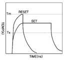
도 2는 GST(Ge2Sb2Te5)를 상변화 막에 사용한 메모리 소자의 리셋/셋 프로그래밍(Reset/Set Programming)을 위한 가열 온도를 나타낸 그래프이다.2 is a graph illustrating a heating temperature for reset / set programming of a memory device using Ge2 Sb2 Te5 (GST) as a phase change film.
도 2를 참조하면, GST의 경우 셋 프로그래밍, 즉 비정질 상태에서 결정 상태로 만들기 위해서는 녹는점보다 낮은 온도에서 어느 정도 시간을 유지하면 결정화가 이루어지는 것을 알 수 있다. 그리고 리셋 프로그래밍, 즉 결정 상태를 비정질 상태로 만들기 위해서는 온도를 거의 녹는점(melting point : Tm)까지 올렸다가 급랭을 시켜야하는 것을 알 수 있다. 녹는점까지 올리기 위해 소비되는 전류 값이 비교적 크기 때문에 고집적 메모리 소자의 구현에 한계가 있다.Referring to FIG. 2, in the case of GST, in order to set programming, that is, to make a crystalline state in an amorphous state, it can be seen that crystallization is performed by maintaining a certain time at a temperature below the melting point. In addition, reset programming, that is, to make the crystal state amorphous, requires that the temperature be raised to a near melting point (Tm) and then quenched. Since the current value consumed to reach the melting point is relatively large, there is a limit to the implementation of highly integrated memory devices.
본 발명에서는 상기 종래 기술의 문제점을 해결하기 위한 것으로, 리셋/셋 프로그래밍을 위한 소비 전류 값을 감소시킬 수 있는 상변화 물질의 프리커서 및 이를 이용한 상변화 메모리 소자의 제조 방법을 제공하는 것을 목적으로 한다.An object of the present invention is to solve the problems of the prior art, and to provide a precursor of a phase change material capable of reducing a current consumption value for reset / set programming and a method of manufacturing a phase change memory device using the same. do.
본 발명에서는 상기 목적을 달성하기 위하여,In the present invention, to achieve the above object,
Ge-Sb-Te 상변화 막 형성을 위한 안티몬 프리커서에 있어서,In antimony precursor for Ge-Sb-Te phase change film formation,
상기 안티몬 프리커서는 안티몬, 질소 및 실리콘이 포함된 프리커서를 제공한다.The antimony precursor provides a precursor containing antimony, nitrogen and silicon.
본 발명에 있어서, 상기 안티몬에 공유 결합한 3개의 질소 및 상기 3개의 질소 각각 공유 결합한 2개의 실리콘을 포함하는 것을 특징으로 한다.In the present invention, it characterized in that it comprises three nitrogen covalently bonded to the antimony and two silicon each covalently bonded to the three nitrogen.
본 발명에 있어서, 상기 실리콘에는 3개의 메틸기가 결합된 것을 특징으로 하는 한다.In the present invention, the silicone is characterized in that three methyl groups are bonded.
본 발명에 있어서, 상기 안티몬 프리커서는 SbN3Si6(Ch3)18의 화학식을 지닌 물질인 것을 특징으로 한다.In the present invention, the antimony precursor is characterized in that the material having a chemical formula of SbN3 Si6 (Ch3 )18 .
또한, 본 발명에서는 반도체 기판; 상기 반도체 기판에 형성된 제 1불순물 영역 및 제 2불순물 영역; 상기 제 1불순물 영역 및 제 2불순물 영역 사이의 채널 영역 상에 형성된 게이트 구조체; 상기 제 2불순물 영역과 연결된 하부 전극; 상기 하부 전극 상에 형성된 상변화 막; 및 상기 상변화 막 상에 형성된 상부 전극을 포함하는 상변화 메모리 소자의 제조 방법에 있어서,In addition, the present invention is a semiconductor substrate; A first impurity region and a second impurity region formed in the semiconductor substrate; A gate structure formed on the channel region between the first impurity region and the second impurity region; A lower electrode connected to the second impurity region; A phase change film formed on the lower electrode; And a top electrode formed on the phase change film.
삭제delete
삭제delete
삭제delete
삭제delete
삭제delete
삭제delete
삭제delete
상기 상변화 막은 안티몬, 질소 및 실리콘이 포함된 안티몬 프리커서에 의해 형성되는 안티몬 프리커서를 이용한 상변화 메모리 소자의 제조 방법을 제공한다.The phase change film provides a method of manufacturing a phase change memory device using an antimony precursor formed by an antimony precursor containing antimony, nitrogen, and silicon.
본 발명에 있어서, 상기 안티몬 프리커서는, SbN3Si6(Ch3)18의 화학식을 지닌 물질인 것을 특징으로 한다.In the present invention, the antimony precursor is characterized in that the material having a chemical formula of SbN3 Si6 (Ch3 )18 .
본 발명에 있어서, 상기 상변화 막은 CVD 또는 ALD에 의해 형성되는 것을 특징으로 한다.In the present invention, the phase change film is formed by CVD or ALD.
이하, 도면을 참조하여 본 발명에 의한 상변화 물질의 프리커서 및 이를 이용한 상변화 메모리 소자의 제조 방법에 대해 상세히 설명하고자 한다.Hereinafter, a precursor of a phase change material and a method of manufacturing a phase change memory device using the same will be described in detail with reference to the accompanying drawings.
도 3은 상변화 막의 종류에 따른 리셋 전류(mA) 값을 나타낸 도면이다. 상부 전극 및 하부 전극으로 TiN을 사용하였고, 그 사이에 상변화 막으로 GST(Ge2Sb2Te5), 질소 도핑된 GST 및 실리콘 도핑된 GST를 사용하여 PRAM을 형성시켰다. 그리고, 상변화 막 상태를 결정 상태에서 비정질 상태로 상변화시킬 수 있는 경우의 전류의 크기, 즉 리셋 전류 값을 측정하였다.3 is a diagram illustrating a reset current (mA) value according to the type of phase change film. TiN was used as the upper electrode and the lower electrode, and a PRAM was formed using GST (Ge2 Sb2 Te5 ), nitrogen doped GST, and silicon doped GST as phase change films therebetween. Then, the magnitude of the current when the phase change film state can be changed from the crystal state to the amorphous state, that is, the reset current value was measured.
도 3을 참조하면, 불순물을 도핑하지 않은 상태의 GST의 경우 리셋 전류의 크기가 3mA로 가장 큰 전류가 필요하였으며, 질소 도핑된 GST의 경우 약 1.5mA의 리셋 전류가 필요한 것을 알 수 있다. 그리고, 실리콘 도핑된 GST를 상변화 막으로 형성시킨 경우에는 가장 낮은 크기인 약 0.7mA의 리셋 전류가 필요한 것을 알 수 있다. 결과적으로 질소 또는 실리콘이 도핑된 경우, GST 상변화 막의 상변화 특성은 그대로 유지되면서 리셋 전류 값이 크게 감소하는 것을 알 수 있다. 이는 실리콘 또는 질소가 GST 상변화 막에 불순물로 포함되면서 비교적 낮은 온도에서 결정 상태에서 비정질 상태로의 상변화를 용이하게 하는 것으로 사료된다.Referring to FIG. 3, it can be seen that the maximum current of 3 mA is required for the GST without doping impurities, and the reset current of about 1.5 mA is required for the GST doped with nitrogen. When the silicon-doped GST is formed of a phase change film, it can be seen that a reset current of about 0.7 mA, which is the lowest size, is required. As a result, when nitrogen or silicon is doped, it can be seen that the reset current value is greatly reduced while maintaining the phase change characteristic of the GST phase change film. This is thought to facilitate the phase change from the crystalline state to the amorphous state at a relatively low temperature as silicon or nitrogen are included as impurities in the GST phase change film.
상변화 물질을 사용하여 메모리 소자의 하부 전극 상에 상변화 막을 형성시키기 위해서는 일반적으로 CVD(Chemical Vapor Deposition : 화학 기상 증착) 또는 ALD(Atomic Layer Deposition : 원자층 증착법) 공정을 이용한다. CVD 또는 ALD 공정을 실시하기 위해서는 프리커서(precursor)가 필수적으로 구비되어야 한다. 현재 질소 또는 실리콘이 도핑된 GST 상변화 막을 얻기 위해서는 먼저 GST 상변화 막을 형성시키고, 질소 또는 실리콘을 별도의 도핑 공정에 의해 GST 상변화 막에 함유시 켜야 한다.In order to form a phase change film on the lower electrode of the memory device using a phase change material, chemical vapor deposition (CVD) or atomic layer deposition (ALD) is generally used. In order to perform a CVD or ALD process, a precursor must be provided. Currently, in order to obtain a GST phase change film doped with nitrogen or silicon, a GST phase change film should be formed first, and nitrogen or silicon should be included in the GST phase change film by a separate doping process.
본 발명자는 이와 같은 GST 상변화 막 형성 공정과 질소 또는 실리콘 도핑 공정을 별도로 행하지 않고도 질소 또는 실리콘 도핑된 GST 상변화 막을 얻을 수 있도록 CVD 또는 ALD 용 프리커서를 제공하고자 실험하였다.The present inventors experimented to provide a precursor for CVD or ALD to obtain a nitrogen or silicon doped GST phase change film without performing such a GST phase change film formation process and a nitrogen or silicon doping process separately.
도 4a 및 도 4b는 본 발명의 실시예의 의한 상변화 물질의 전구체의 제조 순서를 나타낸 도면이다. 본 발명에서는 질소 및 실리콘을 포함하는 안티몬 프리커서를 제공하여 결과적으로 GST 상변화 막이 질소 및 실리콘을 포함되어 GST 상변화 막의 리셋 전류 값을 감소시키는 것을 특징으로 한다.4A and 4B are views illustrating a manufacturing procedure of the precursor of the phase change material according to the embodiment of the present invention. The present invention provides an antimony precursor including nitrogen and silicon, and as a result, the GST phase change film contains nitrogen and silicon, thereby reducing the reset current value of the GST phase change film.
도 4a를 참조하면, H-N-2(Si-3R)(R: 메틸기, CH3)에서 H를 상압에서 노르말 부틸 및 리튬 화합물(nBu-Li)의 리튬과 치환 반응시켜 Li-N-2(Si-3R)을 형성시킨다. 그리고 도 4b에 나타낸 바와 같이, THF(테트라하이드로퓨란 : tetrahydrofuran) 용매 내에서 상온 내지 섭씨 약 150도의 상압에서 3(Li-N-2(Si-3R))을 안티몬 화합물인 SbCl3와 반응시켜 Sb-3(N-2(Si-3R)) 또는 SbN3Si6(Ch3)18의 화학식을 지닌 프리커서를 형성시킨다. 이를 살펴보면, 안티몬 원소에 3개의 질소 원소가 결합되어 있으며, 각각의 질소 원소에 2개의 실리콘 원소가 결합된 것을 알 수 있다.Referring to FIG. 4A, in HN-2 (Si-3R) (R: methyl group, CH3 ), H is substituted and reacted with lithium of normal butyl and lithium compound (nBu-Li) at normal pressure to Li-N-2 (Si). -3R). 4B, 3 (Li-N-2 (Si-3R)) is reacted with antimony compound SbCl3 at room temperature to about 150 degrees Celsius in THF (tetrahydrofuran) solvent. A precursor having the formula -3 (N-2 (Si-3R)) or SbN3 Si6 (Ch3 )18 is formed. Looking at this, it can be seen that three nitrogen elements are bonded to the antimony element, and two silicon elements are bonded to each nitrogen element.
이와 같이 형성된 질소 및 실리콘을 포함하는 안티몬 프리커서를 CVD 또는 ALD 공정의 프리커서로 사용하기 위해서는 고온의 기체 상태로 존재할 수 있도록 질소 및 실리콘이 안티몬에 결합이 된 상태를 유지할 수 있어야 한다. 이를 위해 형성된 안티몬 프리커서 용액을 상온에서부터 온도를 올리며 잔류 물질의 분석을 수행하는 열중량 분석(TGA) 실험을 실시하였다. 도 5는 용매 및 안티몬 프리커서를 포함하는 용액에 대해 열중량 분석 실험을 실시한 결과를 나타낸 그래프이다.In order to use the antimony precursor including nitrogen and silicon thus formed as a precursor in a CVD or ALD process, nitrogen and silicon must remain in an antimony-bonded state to exist in a hot gas state. The antimony precursor solution formed for this purpose was subjected to thermogravimetric analysis (TGA) experiments in which the analysis of residual material was carried out by raising the temperature from room temperature. Figure 5 is a graph showing the results of the thermogravimetric analysis of the solution containing the solvent and antimony precursor.
도 5를 참조하면, 용매 및 도 4b에 나타낸 안티몬 프리커서를 포함하는 용액 13.1790mg에 대해 상온에서부터 가열하였다. 섭씨 약 170도에서 먼저 용매(THF) 약 4.444mg(33.73wt%)이 기화되었다. 그리고, 섭씨 약 310도에서 측정한 결과 2.753mg(20.89wt%)의 탄화 수소(CH3)가 기화된 것을 알 수 있었다. 섭씨 약 1000도까지 온도를 올렸을 때 용매는 거의 대부분 기화되었으며, 잔류하는 물질의 양은 약 4.311mg(32.71wt%)이었다. 이를 조사한 결과 안티몬에 결합된 질소 및 실리콘은 상당량 잔류하는 것을 알 수 있었다. 이는 본 발명에 의해 제조된 질소 및 실리콘을 포함하는 안티몬 프리커서가 CVD 또는 ALD 공정시 프리커서로 유용하게 사용될 수 있음을 의미한다.Referring to Figure 5, it was heated from room temperature for 13.1790 mg of a solution containing a solvent and the antimony precursor shown in Figure 4b. At about 170 degrees Celsius, about 4.444 mg (33.73 wt%) of solvent (THF) was first vaporized. As a result of measuring at about 310 degrees Celsius, 2.753 mg (20.89 wt%) of hydrocarbon (CH3 ) was vaporized. When the temperature was raised to about 1000 degrees Celsius, the solvent almost evaporated and the amount of material remaining was about 4.311 mg (32.71 wt%). As a result of this investigation, it was found that a significant amount of nitrogen and silicon bound to antimony remained. This means that antimony precursors comprising nitrogen and silicon prepared by the present invention can be usefully used as precursors in CVD or ALD processes.
이하, 본 발명에 의해 제조된 질소 및 실리콘을 포함하는 프리커서를 이용하여 상변화 막을 제조한 상변화 메모리 소자 및 그 제조 방법에 대해 상세히 설명하고자 한다.Hereinafter, a phase change memory device for manufacturing a phase change film using a precursor including nitrogen and silicon manufactured by the present invention and a method of manufacturing the same will be described in detail.
도 6은 본 발명에 의해 제조한 상변화 메모리 소자의 일 실시예를 나타낸 단면도이다.6 is a cross-sectional view showing an embodiment of a phase change memory device manufactured according to the present invention.
도 6을 참조하면, n 형 또는 p 형으로 도핑된 반도체 기판(20)에는 반도체 기판(20)과 반대 극성이 되도록 도핑된 제 1불순물 영역(21a) 및 제 2불순물 영역 (21b)이 형성되어 있다. 여기서, 제 1불순물 영역(21a) 및 제 2불순물 영역(21b) 사이의 반도체 기판(20)을 채널 영역이라고 하며, 그 상부에는 게이트 절연층(22) 및 게이트 전극층(23)이 형성되어 있다.Referring to FIG. 6, a
제 1불순물 영역(21a), 게이트 전극층(23) 및 제 2불순물 영역(21b) 상에는 절연층(25)이 형성되어 있으며, 절연층(25) 내에는 제 2불순물 영역(21b)을 노출시키는 콘택 홀이 형성되어 있다. 콘택 홀에는 전도성 플러그(24)가 형성되어 있으며, 그 상부에는 하부 전극(26), 상변화 막(27) 및 상부 전극(28)이 순차적으로 형성되어 있다. 본 발명에 의한 상변화 메모리 소자는 그 상변화 막(27)이 실리콘 및 질소를 포함하는 GST 상변화 막인 것을 특징으로 한다.An insulating
일반적으로 상변화 막(27) 하부의 트랜지스터 구조체는 종래 기술에 의한 반도체 제조 공정에 의하면 용이하게 형성시킬 수 있다. 도 6의 구조에서 하부 전극(26) 및 전도성 플러그(24)를 일체형으로 형성시킬 수 있다. 즉, 전도성 플러그(24)가 직접 하부 전극(26)의 기능을 하도록, 그 상부에 상변화 막(27)을 형성시키고, 전도성 플러그(24)를 통하여 전류를 직접 인가하여 주울 열의 발생을 유도할 수 있다. 이 경우 전도성 플러그(24)는 히팅 플러그(heating plug)로 사용된다.In general, the transistor structure under the
본 발명에 의한 상변화 메모리 소자의 제조 공정을 기술하면 다음과 같다. 먼저, 반도체 기판(20) 상에 게이트 절연층(22) 및 게이트 전극층(23) 물질을 순차적으로 도포한다. 그리고, 게이트 절연층(22) 및 게이트 전극층(23) 물질의 양측부를 제거하여 게이트 절연층(22) 및 게이트 전극층(23)을 완성한다. 노출된 게이트 절연층(22) 및 게이트 전극층(23) 양측 상의 반도체 기판(20) 표면에 불순물을 도 핑하여 제 1불순물 영역(21a) 및 제 2불순물 영역(21b)을 형성시킨다. 그리고 나서, 제 1불순물 영역(21a), 게이트 전극층(23) 및 제 2불순물 영역(21b) 상에 절연층(25)을 형성시킨다. 제 2불순물 영역(21a)이 노출되도록 절연층(25)에 콘택 홀을 형성하고, 콘택 홀 내에 전도성 물질을 충전시켜 전도성 플러그(24)를 형성시킨다.Referring to the manufacturing process of the phase change memory device according to the present invention. First, materials of the gate insulating layer 22 and the gate electrode layer 23 are sequentially applied onto the
선택적으로, 전도성 플러그(24) 상에 전도성 물질인 귀금속 물질 또는 TiN과 같은 금속 질화물 등을 도포하여 하부 전극(26)을 형성시킨다. 전도성 플러그(24) 또는 하부 전극(26) 상에 상변화 막(27)을 형성시키는 경우, 종래 기술에서는 Ge-Sb-Te 물질의 타겟을 이용한 스퍼터링 공정을 주로 사용하였다.Optionally, the
그러나, 본 발명에서는 질소 및 실리콘을 포함하는 안티몬 프리커서를 사용하여 Ge 및 Te 전구체와 함께 반응 챔버 내의 기판 상에서 반응시킴으로써 질소 및 실리콘이 포함된 GST 상변화 막을 얻을 수 있다. 그리고, 상변화 막(27) 상에 하부 전극(26)과 같이 전도성 물질을 도포하여 상부 전극(28)을 형성시킴으로써 본 발명에 의한 상변화 메모리 소자를 완성시킬 수 있다.In the present invention, however, a GST phase change film containing nitrogen and silicon may be obtained by reacting Ge and Te precursors on a substrate in a reaction chamber using an antimony precursor including nitrogen and silicon. In addition, a phase change memory device according to the present invention may be completed by forming a
상기한 설명에서 많은 사항이 구체적으로 기재되어 있으나, 그들은 발명의 범위를 한정하는 것이라기보다, 바람직한 실시예의 예시로서 해석되어야 한다. 따라서, 본 발명의 범위는 설명된 실시예에 의하여 정하여 질 것이 아니고 특허 청구범위에 기재된 기술적 사상에 의해 정하여져야 한다.While many details are set forth in the foregoing description, they should be construed as illustrative of preferred embodiments, rather than to limit the scope of the invention. Therefore, the scope of the present invention should not be defined by the described embodiments, but should be determined by the technical spirit described in the claims.
본 발명에 의하면, 상변화 물질의 프리커서를 제공함으로써, 상변화 막의 결정 구조 변화를 위해 인가하는 전류의 크기를 감소시킬 수 있으며, 이를 통하여 메 모리 소자의 집적화가 가능해짐으로써 고용량의 고속 작동 가능한 반도체 메모리 소자의 구현이 가능한 장점이 있다.According to the present invention, by providing a precursor of a phase change material, it is possible to reduce the amount of current applied to change the crystal structure of the phase change film, thereby enabling the integration of memory devices, thereby enabling high capacity and high speed operation. The semiconductor memory device can be implemented.
Claims (10)
Translated fromKoreanPriority Applications (5)
| Application Number | Priority Date | Filing Date | Title |
|---|---|---|---|
| KR1020040071868AKR100652378B1 (en) | 2004-09-08 | 2004-09-08 | Antimony precursor and manufacturing method of phase change memory device using same |
| US11/219,805US20060049447A1 (en) | 2004-09-08 | 2005-09-07 | Antimony precursor, phase-change memory device using the antimony precursor, and method of manufacturing the phase-change memory device |
| JP2005260193AJP2006080523A (en) | 2004-09-08 | 2005-09-08 | Antimony precursor, phase change memory device and method of manufacturing the same |
| CN200510098148ACN100585899C (en) | 2004-09-08 | 2005-09-08 | Antimony precursor, phase-change memory device using the antimony precursor, and manufacturing method thereof |
| US12/654,839US20100159637A1 (en) | 2004-09-08 | 2010-01-06 | Antimony precursor, phase-change memory device using the antimony precursor, and method of manufacturing the phase-change memory device |
Applications Claiming Priority (1)
| Application Number | Priority Date | Filing Date | Title |
|---|---|---|---|
| KR1020040071868AKR100652378B1 (en) | 2004-09-08 | 2004-09-08 | Antimony precursor and manufacturing method of phase change memory device using same |
Publications (2)
| Publication Number | Publication Date |
|---|---|
| KR20060023049A KR20060023049A (en) | 2006-03-13 |
| KR100652378B1true KR100652378B1 (en) | 2006-12-01 |
Family
ID=36159682
Family Applications (1)
| Application Number | Title | Priority Date | Filing Date |
|---|---|---|---|
| KR1020040071868AExpired - Fee RelatedKR100652378B1 (en) | 2004-09-08 | 2004-09-08 | Antimony precursor and manufacturing method of phase change memory device using same |
Country Status (4)
| Country | Link |
|---|---|
| US (2) | US20060049447A1 (en) |
| JP (1) | JP2006080523A (en) |
| KR (1) | KR100652378B1 (en) |
| CN (1) | CN100585899C (en) |
Families Citing this family (58)
| Publication number | Priority date | Publication date | Assignee | Title |
|---|---|---|---|---|
| KR100640620B1 (en)* | 2004-12-27 | 2006-11-02 | 삼성전자주식회사 | NOR type flash memory device of twin bit cell structure and manufacturing method thereof |
| KR100688532B1 (en)* | 2005-02-14 | 2007-03-02 | 삼성전자주식회사 | Tellurium precursor, Te-containing chalcogenide thin film manufactured using the same, method for manufacturing the thin film and phase change memory device |
| DE102006038885B4 (en)* | 2005-08-24 | 2013-10-10 | Wonik Ips Co., Ltd. | Method for depositing a Ge-Sb-Te thin film |
| KR100695162B1 (en)* | 2005-09-13 | 2007-03-14 | 삼성전자주식회사 | Phase change memory and its operation method |
| KR100695168B1 (en)* | 2006-01-10 | 2007-03-14 | 삼성전자주식회사 | Formation method of phase change material thin film, manufacturing method of phase change memory device using same |
| US7638074B2 (en) | 2006-03-10 | 2009-12-29 | Advanced Technology Materials, Inc. | Precursor compositions for atomic layer deposition and chemical vapor deposition of titanate, lanthanate, and tantalate dielectric films |
| KR101213702B1 (en)* | 2006-04-21 | 2012-12-18 | 삼성전자주식회사 | Non-volatile memory device having a pair of fins between which a void is defined |
| CN101473382A (en)* | 2006-05-12 | 2009-07-01 | 高级技术材料公司 | Low temperature deposition of phase change memory materials |
| US20070267620A1 (en)* | 2006-05-18 | 2007-11-22 | Thomas Happ | Memory cell including doped phase change material |
| KR100763916B1 (en) | 2006-06-21 | 2007-10-05 | 삼성전자주식회사 | Fabrication Method of Thin Film Thin Film and Phase Change Memory Device Using the Same |
| KR100757415B1 (en)* | 2006-07-13 | 2007-09-10 | 삼성전자주식회사 | Germanium compound and manufacturing method thereof, phase change memory device using the germanium compound and forming method thereof |
| KR101169395B1 (en)* | 2006-10-13 | 2012-07-30 | 삼성전자주식회사 | Method of manufacturing phase change memory device comprising surface treatment process of phase change layer |
| KR100902504B1 (en)* | 2006-10-16 | 2009-06-15 | 삼성전자주식회사 | A resistive memory device comprising an amorphous solid electrolyte layer and a method of operating the same |
| CN102352488B (en)* | 2006-11-02 | 2016-04-06 | 诚实公司 | The antimony useful for the CVD/ALD of metallic film and germanium complexes |
| KR101275799B1 (en)* | 2006-11-21 | 2013-06-18 | 삼성전자주식회사 | Method of forming phase change layer using Ge precursor for low temperature deposition and method of manufacturing phase change memory device using the same |
| US7718989B2 (en)* | 2006-12-28 | 2010-05-18 | Macronix International Co., Ltd. | Resistor random access memory cell device |
| US7820474B2 (en)* | 2007-01-09 | 2010-10-26 | International Business Machines Corporation | Metal catalyzed selective deposition of materials including germanium and antimony |
| US8377341B2 (en)* | 2007-04-24 | 2013-02-19 | Air Products And Chemicals, Inc. | Tellurium (Te) precursors for making phase change memory materials |
| CN100582002C (en)* | 2007-04-29 | 2010-01-20 | 中国科学院上海微系统与信息技术研究所 | Storage material without tellurium, preparation method and application |
| US7678642B2 (en)* | 2007-05-11 | 2010-03-16 | Hynix Semiconductor Inc. | Method for manufacturing phase change memory device using a patterning process |
| KR100888617B1 (en) | 2007-06-15 | 2009-03-17 | 삼성전자주식회사 | Phase change memory device and forming method thereof |
| KR101593352B1 (en)* | 2007-06-28 | 2016-02-15 | 인티그리스, 인코포레이티드 | Precursors for silicon dioxide gap fill |
| US8455049B2 (en)* | 2007-08-08 | 2013-06-04 | Advanced Technology Materials, Inc. | Strontium precursor for use in chemical vapor deposition, atomic layer deposition and rapid vapor deposition |
| KR101458953B1 (en) | 2007-10-11 | 2014-11-07 | 삼성전자주식회사 | Method of forming phase change material layer using Ge(Ⅱ) source, and method of fabricating phase change memory device |
| US8834968B2 (en) | 2007-10-11 | 2014-09-16 | Samsung Electronics Co., Ltd. | Method of forming phase change material layer using Ge(II) source, and method of fabricating phase change memory device |
| SG178736A1 (en)* | 2007-10-31 | 2012-03-29 | Advanced Tech Materials | Amorphous ge/te deposition process |
| US20100279011A1 (en)* | 2007-10-31 | 2010-11-04 | Advanced Technology Materials, Inc. | Novel bismuth precursors for cvd/ald of thin films |
| US7960205B2 (en)* | 2007-11-27 | 2011-06-14 | Air Products And Chemicals, Inc. | Tellurium precursors for GST films in an ALD or CVD process |
| US7897953B2 (en)* | 2008-01-16 | 2011-03-01 | Micron Technology, Inc. | Multi-level programmable PCRAM memory |
| JP5341107B2 (en)* | 2008-01-25 | 2013-11-13 | インターナショナル・ビジネス・マシーンズ・コーポレーション | Selective deposition of materials containing germanium and antimony using metal catalysts |
| US8318252B2 (en) | 2008-01-28 | 2012-11-27 | Air Products And Chemicals, Inc. | Antimony precursors for GST films in ALD/CVD processes |
| US20090215225A1 (en)* | 2008-02-24 | 2009-08-27 | Advanced Technology Materials, Inc. | Tellurium compounds useful for deposition of tellurium containing materials |
| US8674127B2 (en) | 2008-05-02 | 2014-03-18 | Advanced Technology Materials, Inc. | Antimony compounds useful for deposition of antimony-containing materials |
| US8765223B2 (en) | 2008-05-08 | 2014-07-01 | Air Products And Chemicals, Inc. | Binary and ternary metal chalcogenide materials and method of making and using same |
| US8507040B2 (en) | 2008-05-08 | 2013-08-13 | Air Products And Chemicals, Inc. | Binary and ternary metal chalcogenide materials and method of making and using same |
| US20110180905A1 (en)* | 2008-06-10 | 2011-07-28 | Advanced Technology Materials, Inc. | GeSbTe MATERIAL INCLUDING SUPERFLOW LAYER(S), AND USE OF Ge TO PREVENT INTERACTION OF Te FROM SbXTeY AND GeXTeY RESULTING IN HIGH Te CONTENT AND FILM CRYSTALLINITY |
| WO2010065874A2 (en) | 2008-12-05 | 2010-06-10 | Atmi | High concentration nitrogen-containing germanium telluride based memory devices and processes of making |
| KR20160084491A (en) | 2009-05-22 | 2016-07-13 | 엔테그리스, 아이엔씨. | Low temperature gst process |
| KR101602007B1 (en)* | 2009-07-02 | 2016-03-09 | 인티그리스, 인코포레이티드 | Hollow gst structure with dielectric fill |
| US20110108792A1 (en)* | 2009-11-11 | 2011-05-12 | International Business Machines Corporation | Single Crystal Phase Change Material |
| US20110124182A1 (en)* | 2009-11-20 | 2011-05-26 | Advanced Techology Materials, Inc. | System for the delivery of germanium-based precursor |
| TW201132787A (en) | 2010-03-26 | 2011-10-01 | Advanced Tech Materials | Germanium antimony telluride materials and devices incorporating same |
| WO2011146913A2 (en) | 2010-05-21 | 2011-11-24 | Advanced Technology Materials, Inc. | Germanium antimony telluride materials and devices incorporating same |
| KR101094987B1 (en) | 2010-07-06 | 2011-12-20 | 주식회사 하이닉스반도체 | Phase change memory device and manufacturing method thereof |
| US9373677B2 (en) | 2010-07-07 | 2016-06-21 | Entegris, Inc. | Doping of ZrO2 for DRAM applications |
| US8426242B2 (en)* | 2011-02-01 | 2013-04-23 | Macronix International Co., Ltd. | Composite target sputtering for forming doped phase change materials |
| TWI452167B (en) | 2011-06-09 | 2014-09-11 | Air Prod & Chem | Binary and ternary metal chalcogenide materials and method of making and using same |
| US8946666B2 (en) | 2011-06-23 | 2015-02-03 | Macronix International Co., Ltd. | Ge-Rich GST-212 phase change memory materials |
| US8932901B2 (en) | 2011-10-31 | 2015-01-13 | Macronix International Co., Ltd. | Stressed phase change materials |
| US20130243971A1 (en)* | 2012-03-14 | 2013-09-19 | Applied Materials, Inc. | Apparatus and Process for Atomic Layer Deposition with Horizontal Laser |
| KR102117124B1 (en) | 2012-04-30 | 2020-05-29 | 엔테그리스, 아이엔씨. | Phase change memory structure comprising phase change alloy center-filled with dielectric material |
| WO2013177326A1 (en) | 2012-05-25 | 2013-11-28 | Advanced Technology Materials, Inc. | Silicon precursors for low temperature ald of silicon-based thin-films |
| JP5905858B2 (en) | 2012-08-13 | 2016-04-20 | エア プロダクツ アンド ケミカルズ インコーポレイテッドAir Products And Chemicals Incorporated | Precursor for GST film in ALD / CVD process |
| US9640757B2 (en) | 2012-10-30 | 2017-05-02 | Entegris, Inc. | Double self-aligned phase change memory device structure |
| WO2014124056A1 (en) | 2013-02-08 | 2014-08-14 | Advanced Technology Materials, Inc. | Ald processes for low leakage current and low equivalent oxide thickness bitao films |
| US9336879B2 (en) | 2014-01-24 | 2016-05-10 | Macronix International Co., Ltd. | Multiple phase change materials in an integrated circuit for system on a chip application |
| WO2018017216A1 (en)* | 2016-07-18 | 2018-01-25 | Applied Materials, Inc. | A method and material for cmos contact and barrier layer |
| KR102819579B1 (en) | 2022-12-06 | 2025-06-12 | 한국화학연구원 | Novel germanium precursor, composition for thin film deposition containing the same, and method for manufacturing a thin film employing the same |
Citations (1)
| Publication number | Priority date | Publication date | Assignee | Title |
|---|---|---|---|---|
| JPH11345438A (en) | 1998-03-20 | 1999-12-14 | Sony Corp | Optical recording medium and manufacturing method thereof |
Family Cites Families (5)
| Publication number | Priority date | Publication date | Assignee | Title |
|---|---|---|---|---|
| JP2000236075A (en)* | 1999-02-12 | 2000-08-29 | Sony Corp | Method for manufacturing dielectric capacitor and method for manufacturing semiconductor memory device |
| KR100815009B1 (en)* | 2000-09-28 | 2008-03-18 | 프레지던트 앤드 펠로우즈 오브 하바드 칼리지 | Precipitation Using Vapors of Oxides, Silicates and Phosphates |
| US7402851B2 (en)* | 2003-02-24 | 2008-07-22 | Samsung Electronics Co., Ltd. | Phase changeable memory devices including nitrogen and/or silicon and methods for fabricating the same |
| US7411208B2 (en)* | 2004-05-27 | 2008-08-12 | Samsung Electronics Co., Ltd. | Phase-change memory device having a barrier layer and manufacturing method |
| KR100653701B1 (en)* | 2004-08-20 | 2006-12-04 | 삼성전자주식회사 | Method for forming small via structure of semiconductor device and manufacturing method of phase change memory device using same |
- 2004
- 2004-09-08KRKR1020040071868Apatent/KR100652378B1/ennot_activeExpired - Fee Related
- 2005
- 2005-09-07USUS11/219,805patent/US20060049447A1/ennot_activeAbandoned
- 2005-09-08CNCN200510098148Apatent/CN100585899C/ennot_activeExpired - Fee Related
- 2005-09-08JPJP2005260193Apatent/JP2006080523A/ennot_activeWithdrawn
- 2010
- 2010-01-06USUS12/654,839patent/US20100159637A1/ennot_activeAbandoned
Patent Citations (1)
| Publication number | Priority date | Publication date | Assignee | Title |
|---|---|---|---|---|
| JPH11345438A (en) | 1998-03-20 | 1999-12-14 | Sony Corp | Optical recording medium and manufacturing method thereof |
Also Published As
| Publication number | Publication date |
|---|---|
| CN100585899C (en) | 2010-01-27 |
| JP2006080523A (en) | 2006-03-23 |
| CN1763987A (en) | 2006-04-26 |
| KR20060023049A (en) | 2006-03-13 |
| US20100159637A1 (en) | 2010-06-24 |
| US20060049447A1 (en) | 2006-03-09 |
Similar Documents
| Publication | Publication Date | Title |
|---|---|---|
| KR100652378B1 (en) | Antimony precursor and manufacturing method of phase change memory device using same | |
| KR100688532B1 (en) | Tellurium precursor, Te-containing chalcogenide thin film manufactured using the same, method for manufacturing the thin film and phase change memory device | |
| KR100618879B1 (en) | Germanium precursor, UST thin film formed using the same, method for manufacturing the thin film and phase change memory device | |
| JP5148063B2 (en) | Germanium precursor, GST thin film formed using the same, method for manufacturing the thin film, and phase change memory device | |
| KR100585175B1 (en) | Method for manufacturing thin film thin film by chemical vapor deposition | |
| CN1996608B (en) | Phase change materials, phase change random access memories having the same and methods of operating phase change random access memories | |
| KR100763916B1 (en) | Fabrication Method of Thin Film Thin Film and Phase Change Memory Device Using the Same | |
| US7456420B2 (en) | Electrode for phase change memory device and method | |
| KR100873878B1 (en) | Manufacturing method of phase change memory unit and manufacturing method of phase change memory device using same | |
| JP5160086B2 (en) | Method for manufacturing phase change memory device having fullerene layer | |
| US20080173860A1 (en) | Phase change memory device and method of fabricating the same | |
| JP5043044B2 (en) | Manufacturing method of semiconductor memory device | |
| US20090161406A1 (en) | Non-volatile memory and method for fabricating the same | |
| US7767491B2 (en) | Methods of manufacturing semiconductor device | |
| CN106997924B (en) | Phase transition storage and its manufacturing method and electronic equipment | |
| US20130193402A1 (en) | Phase-change random access memory device and method of manufacturing the same | |
| KR100738115B1 (en) | Phase change memory device having a doped phase change layer and a method of operating the same | |
| KR20070033743A (en) | Method for manufacturing amorphous NiO thin film by ALD process and nonvolatile memory device using amorphous NiI thin film | |
| JP7097599B2 (en) | Phase change material and phase change type memory element using phase change material | |
| KR20080040238A (en) | Selenium doped phase change material and phase change memory device including the same | |
| US8729522B2 (en) | Memory constructions comprising thin films of phase change material | |
| KR20100054261A (en) | Phase change random access memory device and manufacturing method thereof | |
| KR20090052660A (en) | Phase change memory device and forming method thereof |
Legal Events
| Date | Code | Title | Description |
|---|---|---|---|
| A201 | Request for examination | ||
| PA0109 | Patent application | St.27 status event code:A-0-1-A10-A12-nap-PA0109 | |
| PA0201 | Request for examination | St.27 status event code:A-1-2-D10-D11-exm-PA0201 | |
| R17-X000 | Change to representative recorded | St.27 status event code:A-3-3-R10-R17-oth-X000 | |
| PN2301 | Change of applicant | St.27 status event code:A-3-3-R10-R13-asn-PN2301 St.27 status event code:A-3-3-R10-R11-asn-PN2301 | |
| PN2301 | Change of applicant | St.27 status event code:A-3-3-R10-R13-asn-PN2301 St.27 status event code:A-3-3-R10-R11-asn-PN2301 | |
| D13-X000 | Search requested | St.27 status event code:A-1-2-D10-D13-srh-X000 | |
| D14-X000 | Search report completed | St.27 status event code:A-1-2-D10-D14-srh-X000 | |
| PG1501 | Laying open of application | St.27 status event code:A-1-1-Q10-Q12-nap-PG1501 | |
| E902 | Notification of reason for refusal | ||
| PE0902 | Notice of grounds for rejection | St.27 status event code:A-1-2-D10-D21-exm-PE0902 | |
| T11-X000 | Administrative time limit extension requested | St.27 status event code:U-3-3-T10-T11-oth-X000 | |
| E13-X000 | Pre-grant limitation requested | St.27 status event code:A-2-3-E10-E13-lim-X000 | |
| P11-X000 | Amendment of application requested | St.27 status event code:A-2-2-P10-P11-nap-X000 | |
| P13-X000 | Application amended | St.27 status event code:A-2-2-P10-P13-nap-X000 | |
| E701 | Decision to grant or registration of patent right | ||
| PE0701 | Decision of registration | St.27 status event code:A-1-2-D10-D22-exm-PE0701 | |
| GRNT | Written decision to grant | ||
| PR0701 | Registration of establishment | St.27 status event code:A-2-4-F10-F11-exm-PR0701 | |
| PR1002 | Payment of registration fee | St.27 status event code:A-2-2-U10-U11-oth-PR1002 Fee payment year number:1 | |
| PG1601 | Publication of registration | St.27 status event code:A-4-4-Q10-Q13-nap-PG1601 | |
| PR1001 | Payment of annual fee | St.27 status event code:A-4-4-U10-U11-oth-PR1001 Fee payment year number:4 | |
| PR1001 | Payment of annual fee | St.27 status event code:A-4-4-U10-U11-oth-PR1001 Fee payment year number:5 | |
| PR1001 | Payment of annual fee | St.27 status event code:A-4-4-U10-U11-oth-PR1001 Fee payment year number:6 | |
| R18-X000 | Changes to party contact information recorded | St.27 status event code:A-5-5-R10-R18-oth-X000 | |
| FPAY | Annual fee payment | Payment date:20121031 Year of fee payment:7 | |
| PR1001 | Payment of annual fee | St.27 status event code:A-4-4-U10-U11-oth-PR1001 Fee payment year number:7 | |
| FPAY | Annual fee payment | Payment date:20131031 Year of fee payment:8 | |
| PR1001 | Payment of annual fee | St.27 status event code:A-4-4-U10-U11-oth-PR1001 Fee payment year number:8 | |
| LAPS | Lapse due to unpaid annual fee | ||
| PC1903 | Unpaid annual fee | St.27 status event code:A-4-4-U10-U13-oth-PC1903 Not in force date:20141125 Payment event data comment text:Termination Category : DEFAULT_OF_REGISTRATION_FEE | |
| PC1903 | Unpaid annual fee | St.27 status event code:N-4-6-H10-H13-oth-PC1903 Ip right cessation event data comment text:Termination Category : DEFAULT_OF_REGISTRATION_FEE Not in force date:20141125 | |
| P22-X000 | Classification modified | St.27 status event code:A-4-4-P10-P22-nap-X000 | |
| P22-X000 | Classification modified | St.27 status event code:A-4-4-P10-P22-nap-X000 |