KR100650400B1 - Array substrate for liquid crystal display device and manufacturing method thereof - Google Patents
Array substrate for liquid crystal display device and manufacturing method thereofDownload PDFInfo
- Publication number
- KR100650400B1 KR100650400B1KR1020000085414AKR20000085414AKR100650400B1KR 100650400 B1KR100650400 B1KR 100650400B1KR 1020000085414 AKR1020000085414 AKR 1020000085414AKR 20000085414 AKR20000085414 AKR 20000085414AKR 100650400 B1KR100650400 B1KR 100650400B1
- Authority
- KR
- South Korea
- Prior art keywords
- gate
- light blocking
- data line
- layer
- electrode
- Prior art date
- Legal status (The legal status is an assumption and is not a legal conclusion. Google has not performed a legal analysis and makes no representation as to the accuracy of the status listed.)
- Expired - Fee Related
Links
Images


Classifications
- G—PHYSICS
- G02—OPTICS
- G02F—OPTICAL DEVICES OR ARRANGEMENTS FOR THE CONTROL OF LIGHT BY MODIFICATION OF THE OPTICAL PROPERTIES OF THE MEDIA OF THE ELEMENTS INVOLVED THEREIN; NON-LINEAR OPTICS; FREQUENCY-CHANGING OF LIGHT; OPTICAL LOGIC ELEMENTS; OPTICAL ANALOGUE/DIGITAL CONVERTERS
- G02F1/00—Devices or arrangements for the control of the intensity, colour, phase, polarisation or direction of light arriving from an independent light source, e.g. switching, gating or modulating; Non-linear optics
- G02F1/01—Devices or arrangements for the control of the intensity, colour, phase, polarisation or direction of light arriving from an independent light source, e.g. switching, gating or modulating; Non-linear optics for the control of the intensity, phase, polarisation or colour
- G02F1/13—Devices or arrangements for the control of the intensity, colour, phase, polarisation or direction of light arriving from an independent light source, e.g. switching, gating or modulating; Non-linear optics for the control of the intensity, phase, polarisation or colour based on liquid crystals, e.g. single liquid crystal display cells
- G02F1/133—Constructional arrangements; Operation of liquid crystal cells; Circuit arrangements
- G02F1/1333—Constructional arrangements; Manufacturing methods
- G02F1/1335—Structural association of cells with optical devices, e.g. polarisers or reflectors
- G02F1/133509—Filters, e.g. light shielding masks
- G02F1/133514—Colour filters
- G—PHYSICS
- G02—OPTICS
- G02F—OPTICAL DEVICES OR ARRANGEMENTS FOR THE CONTROL OF LIGHT BY MODIFICATION OF THE OPTICAL PROPERTIES OF THE MEDIA OF THE ELEMENTS INVOLVED THEREIN; NON-LINEAR OPTICS; FREQUENCY-CHANGING OF LIGHT; OPTICAL LOGIC ELEMENTS; OPTICAL ANALOGUE/DIGITAL CONVERTERS
- G02F1/00—Devices or arrangements for the control of the intensity, colour, phase, polarisation or direction of light arriving from an independent light source, e.g. switching, gating or modulating; Non-linear optics
- G02F1/01—Devices or arrangements for the control of the intensity, colour, phase, polarisation or direction of light arriving from an independent light source, e.g. switching, gating or modulating; Non-linear optics for the control of the intensity, phase, polarisation or colour
- G02F1/13—Devices or arrangements for the control of the intensity, colour, phase, polarisation or direction of light arriving from an independent light source, e.g. switching, gating or modulating; Non-linear optics for the control of the intensity, phase, polarisation or colour based on liquid crystals, e.g. single liquid crystal display cells
- G02F1/133—Constructional arrangements; Operation of liquid crystal cells; Circuit arrangements
- G02F1/136—Liquid crystal cells structurally associated with a semi-conducting layer or substrate, e.g. cells forming part of an integrated circuit
- G02F1/1362—Active matrix addressed cells
- G02F1/136286—Wiring, e.g. gate line, drain line
- G—PHYSICS
- G02—OPTICS
- G02F—OPTICAL DEVICES OR ARRANGEMENTS FOR THE CONTROL OF LIGHT BY MODIFICATION OF THE OPTICAL PROPERTIES OF THE MEDIA OF THE ELEMENTS INVOLVED THEREIN; NON-LINEAR OPTICS; FREQUENCY-CHANGING OF LIGHT; OPTICAL LOGIC ELEMENTS; OPTICAL ANALOGUE/DIGITAL CONVERTERS
- G02F1/00—Devices or arrangements for the control of the intensity, colour, phase, polarisation or direction of light arriving from an independent light source, e.g. switching, gating or modulating; Non-linear optics
- G02F1/01—Devices or arrangements for the control of the intensity, colour, phase, polarisation or direction of light arriving from an independent light source, e.g. switching, gating or modulating; Non-linear optics for the control of the intensity, phase, polarisation or colour
- G02F1/13—Devices or arrangements for the control of the intensity, colour, phase, polarisation or direction of light arriving from an independent light source, e.g. switching, gating or modulating; Non-linear optics for the control of the intensity, phase, polarisation or colour based on liquid crystals, e.g. single liquid crystal display cells
- G02F1/133—Constructional arrangements; Operation of liquid crystal cells; Circuit arrangements
- G02F1/136—Liquid crystal cells structurally associated with a semi-conducting layer or substrate, e.g. cells forming part of an integrated circuit
- G02F1/13606—Liquid crystal cells structurally associated with a semi-conducting layer or substrate, e.g. cells forming part of an integrated circuit having means for reducing parasitic capacitance
- G—PHYSICS
- G02—OPTICS
- G02F—OPTICAL DEVICES OR ARRANGEMENTS FOR THE CONTROL OF LIGHT BY MODIFICATION OF THE OPTICAL PROPERTIES OF THE MEDIA OF THE ELEMENTS INVOLVED THEREIN; NON-LINEAR OPTICS; FREQUENCY-CHANGING OF LIGHT; OPTICAL LOGIC ELEMENTS; OPTICAL ANALOGUE/DIGITAL CONVERTERS
- G02F1/00—Devices or arrangements for the control of the intensity, colour, phase, polarisation or direction of light arriving from an independent light source, e.g. switching, gating or modulating; Non-linear optics
- G02F1/01—Devices or arrangements for the control of the intensity, colour, phase, polarisation or direction of light arriving from an independent light source, e.g. switching, gating or modulating; Non-linear optics for the control of the intensity, phase, polarisation or colour
- G02F1/13—Devices or arrangements for the control of the intensity, colour, phase, polarisation or direction of light arriving from an independent light source, e.g. switching, gating or modulating; Non-linear optics for the control of the intensity, phase, polarisation or colour based on liquid crystals, e.g. single liquid crystal display cells
- G02F1/133—Constructional arrangements; Operation of liquid crystal cells; Circuit arrangements
- G02F1/136—Liquid crystal cells structurally associated with a semi-conducting layer or substrate, e.g. cells forming part of an integrated circuit
- G02F1/1362—Active matrix addressed cells
- G02F1/136231—Active matrix addressed cells for reducing the number of lithographic steps
- G—PHYSICS
- G02—OPTICS
- G02F—OPTICAL DEVICES OR ARRANGEMENTS FOR THE CONTROL OF LIGHT BY MODIFICATION OF THE OPTICAL PROPERTIES OF THE MEDIA OF THE ELEMENTS INVOLVED THEREIN; NON-LINEAR OPTICS; FREQUENCY-CHANGING OF LIGHT; OPTICAL LOGIC ELEMENTS; OPTICAL ANALOGUE/DIGITAL CONVERTERS
- G02F1/00—Devices or arrangements for the control of the intensity, colour, phase, polarisation or direction of light arriving from an independent light source, e.g. switching, gating or modulating; Non-linear optics
- G02F1/01—Devices or arrangements for the control of the intensity, colour, phase, polarisation or direction of light arriving from an independent light source, e.g. switching, gating or modulating; Non-linear optics for the control of the intensity, phase, polarisation or colour
- G02F1/13—Devices or arrangements for the control of the intensity, colour, phase, polarisation or direction of light arriving from an independent light source, e.g. switching, gating or modulating; Non-linear optics for the control of the intensity, phase, polarisation or colour based on liquid crystals, e.g. single liquid crystal display cells
- G02F1/133—Constructional arrangements; Operation of liquid crystal cells; Circuit arrangements
- G02F1/136—Liquid crystal cells structurally associated with a semi-conducting layer or substrate, e.g. cells forming part of an integrated circuit
- G02F1/1362—Active matrix addressed cells
- G02F1/136259—Repairing; Defects
- G02F1/136263—Line defects
Landscapes
- Physics & Mathematics (AREA)
- Nonlinear Science (AREA)
- Mathematical Physics (AREA)
- Chemical & Material Sciences (AREA)
- Crystallography & Structural Chemistry (AREA)
- General Physics & Mathematics (AREA)
- Optics & Photonics (AREA)
- Engineering & Computer Science (AREA)
- Microelectronics & Electronic Packaging (AREA)
- Liquid Crystal (AREA)
- Thin Film Transistor (AREA)
Abstract
Translated fromKoreanDescription
Translated fromKorean도 1은 일반적인 액정 표시 장치의 단면도.1 is a cross-sectional view of a general liquid crystal display device.
도 2는 일반적인 액정 표시 장치용 어레이 기판의 평면도.2 is a plan view of an array substrate for a general liquid crystal display device.
도 3은 본 발명에 따른 액정 표시 장치용 어레이 기판의 평면도.3 is a plan view of an array substrate for a liquid crystal display device according to the present invention;
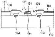
도 4는 도 3에서 Ⅳ-Ⅳ선을 따라 자른 단면도.4 is a cross-sectional view taken along the line IV-IV of FIG. 3.
도 5는 도 3에서 Ⅴ-Ⅴ선을 따라 자른 단면도.FIG. 5 is a cross-sectional view taken along the line VV of FIG. 3. FIG.
도 6a 내지 도 6d와 도 7a 내지 도 7d는 본 발명에 따라 어레이 기판을 제조하는 공정을 도시한 단면도.6A-6D and 7A-7D are cross-sectional views illustrating a process of fabricating an array substrate in accordance with the present invention.
도 8은 본 발명에 따른 마스크에 대한 단면도.
8 is a cross-sectional view of a mask according to the present invention.
본 발명은 액정 표시 장치 및 그의 제조 방법에 관한 것으로서, 더욱 상세하게는 액정 표시 장치용 어레이 기판 및 그의 제조 방법에 관한 것이다.BACKGROUND OF THE INVENTION 1. Field of the Invention The present invention relates to a liquid crystal display device and a manufacturing method thereof, and more particularly, to an array substrate for a liquid crystal display device and a manufacturing method thereof.
최근 정보화 사회로 시대가 급발전함에 따라 박형화, 경량화, 저 소비전력화 등의 우수한 특성을 가지는 평판 표시장치(flat panel display)의 필요성이 대두되었는데, 그 중 색 재현성 등이 우수한 액정 표시 장치(liquid crystal display)가 활발하게 개발되고 있다.Recently, with the rapid development of the information society, there is a need for a flat panel display having excellent characteristics such as thinning, light weight, and low power consumption. Among them, a liquid crystal display having excellent color reproducibility, etc. displays are actively being developed.
일반적으로 액정 표시 장치는 전극이 각각 형성되어 있는 두 기판을 두 전극이 형성되어 있는 면이 마주 대하도록 배치하고 두 기판 사이에 액정 물질을 주입한 다음, 두 전극에 전압을 인가하여 생성되는 전기장에 의해 액정 분자를 움직이게 함으로써, 이에 따라 달라지는 빛의 투과율에 의해 화상을 표현하는 장치이다.In general, a liquid crystal display device arranges two substrates on which electrodes are formed so that the surfaces on which the two electrodes are formed face each other, injects a liquid crystal material between the two substrates, and applies a voltage to the two electrodes to generate an electric field. By moving the liquid crystal molecules, the image is expressed by the transmittance of light that varies accordingly.
이하, 첨부한 도면을 참조하여 일반적인 액정 표시 장치의 구조에 대하여 설명한다.Hereinafter, a structure of a general liquid crystal display device will be described with reference to the accompanying drawings.
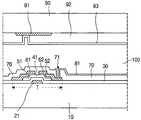
도 1은 일반적인 액정 표시 장치에 대한 단면도이다.1 is a cross-sectional view of a general liquid crystal display.
도 1에 도시한 바와 같이, 투명한 제 1 기판(10) 위에 금속과 같은 도전 물질로 이루어진 게이트 전극(21)이 형성되어 있고, 그 위에 실리콘 질화막(SiNx)이나 실리콘 산화막(SiO2)으로 이루어진 게이트 절연막(30)이 게이트 전극(21)을 덮고 있다. 게이트 전극(21) 상부의 게이트 절연막(30) 위에는 비정질 실리콘으로 이루어진 액티브층(41)이 형성되어 있으며, 그 위에 불순물이 도핑된 비정질 실리콘으로 이루어진 오믹 콘택층(51, 52)이 형성되어 있다.As shown in FIG. 1, a
오믹 콘택층(51, 52) 상부에는 금속과 같은 도전 물질로 이루어진 소스 및 드레인 전극(61, 62)이 형성되어 있는데, 소스 및 드레인 전극(61, 62)은 게이트 전극(21)과 함께 박막 트랜지스터(T)를 이룬다.Source and
이어, 소스 및 드레인 전극(61, 62) 위에는 실리콘 질화막이나 실리콘 산화막 또는 유기 절연막으로 이루어진 보호층(70)이 형성되어 있으며, 보호층(70)은 드레인 전극(62)을 드러내는 콘택홀(71)을 가진다.Next, a
보호층(70) 상부에는 투명 도전 물질로 이루어진 화소 전극(81)이 형성되어 있고, 화소 전극(81)은 콘택홀(71)을 통해 드레인 전극(62)과 연결되어 있다.A
한편, 제 1 기판(10) 상부에는 제 1 기판(10)과 일정 간격을 가지고 이격되어 있으며 투명한 제 2 기판(90)이 배치되어 있고, 제 2 기판(90)의 안쪽면에는 블랙 매트릭스(91)가 박막 트랜지스터(T)와 대응되는 위치에 형성되어 있다. 블랙 매트릭스(91) 하부에는 컬러 필터(92)가 형성되어 있는데, 컬러 필터(92)는 적(R), 녹(G), 청(B)의 색이 순차적으로 반복되어 있으며, 하나의 색이 하나의 화소 영역에 대응된다. 컬러 필터(92) 하부에는 투명한 도전 물질로 이루어진 공통 전극(93)이 형성되어 있다.On the other hand, the
그리고, 두 기판(10, 90) 사이에는 액정층(100)이 주입되어 있다.The
이러한 액정 표시 장치는 하부의 어레이 기판과 상부의 컬러 필터 기판을 각각 형성하고, 하부의 화소 전극과 상부의 컬러 필터가 일대일 대응되도록 배치하는 공정을 통해 형성된다.The liquid crystal display is formed by forming a lower array substrate and an upper color filter substrate, and arranging the lower pixel electrode and the upper color filter in a one-to-one correspondence.
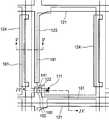
도 2에 일반적인 액정 표시 장치용 어레이 기판에 대한 평면도를 도시하였다.2 is a plan view of an array substrate for a general liquid crystal display device.
도 2에 도시한 바와 같이, 가로 방향의 게이트 배선(22)과 세로 방향의 데이 터 배선(63)이 교차하고, 게이트 배선(22)과 데이터 배선(63)의 교차점에는 박막 트랜지스터(T)가 형성되어 있다.As shown in FIG. 2, the thin film transistor T is disposed at the intersection of the
게이트 배선(22)과 데이터 배선(63)에 의해 정의되는 화소 영역에는 화소 전극(81)이 형성되어 있고, 화소 전극(81)은 박막 트랜지스터(T)와 연결되어 있다. 또한, 화소 전극(81)은 게이트 배선(22)과 일부 중첩하여 게이트 배선(22)과 함께 스토리지 캐패시터(storage capacitor)를 형성한다.The
이러한 어레이 기판과 컬러 필터 기판을 배치할 때, 화소 전극(81)과 컬러 필터는 일대일 대응해야 하며, 상부의 블랙 매트릭스는 화소 전극(81)을 제외한 영역을 가리도록 배치되어야 하는데, 블랙 매트릭스와 화소 전극(81)의 가장자리 부분을 정확하게 맞추기가 어렵다. 따라서, 오정렬(misalign)이 발생할 확률이 높고, 오정렬이 발생할 경우 블랙 매트릭스와 화소 전극(81) 사이에 틈이 생기게 되어, 이 부분에서 빛샘이 일어날 수 있다.When arranging the array substrate and the color filter substrate, the
이를 방지하기 위해, 블랙 매트릭스는 합착마진을 고려하여 폭을 더 넓게 형성함으로써, 합착마진만큼 화소 전극과 중첩되도록 한다. 이때, 합착마진은 개구율과 같은 문제를 고려하여 5 ㎛ 정도로 한다.In order to prevent this, the black matrix is formed to be wider in consideration of the bonding margin, so that the black matrix overlaps the pixel electrode by the bonding margin. In this case, the bonding margin is about 5 μm in consideration of problems such as aperture ratio.
그러나, 컬러 필터 기판과 어레이 기판을 합착시키고 이후 공정을 진행할 경우, 공정의 온도 등에 따라 기판의 크기가 달라질 수 있는데, 컬러 필터 기판과 어레이 기판은 그 종류가 다르기 때문에 기판의 크기 변화 정도가 각각 다르게 된다. 이에 따라, 블랙 매트릭스의 폭을 넓게 하더라도, 블랙 매트릭스와 화소 전극 사이에 어긋나는 부분이 생겨 빛이 새는 문제가 발생한다.However, when the color filter substrate and the array substrate are bonded to each other and the subsequent process is performed, the size of the substrate may vary depending on the temperature of the process. do. As a result, even if the width of the black matrix is widened, there is a problem that light is leaked due to a portion that is displaced between the black matrix and the pixel electrode.
한편, 액정 표시 장치의 어레이 기판은 박막을 형성하고 사진 식각하는 공정을 반복함으로써 이루어지는데, 사진 식각 공정에는 세정, 감광막 도포, 노광 및 현상, 식각 등 여러 공정을 수반하고 있다. 따라서, 사진 식각 공정을 한번만 단축해도 제조 시간이 상당히 많이 줄어들고 제조 비용이 감소된다. 일반적으로 사진 식각 공정에 이용되는 마스크 수가 공정수를 대표한다. 도 2와 같은 구조를 가지는 어레이 기판은 5장의 마스크를 이용하여 제조되는데, 마스크 수를 감소시켜 제조 비용을 줄일 필요가 있다.
Meanwhile, an array substrate of a liquid crystal display device is formed by repeating a process of forming a thin film and performing photolithography. The photolithography process involves various processes such as cleaning, photoresist coating, exposure and development, and etching. Thus, shortening the photolithography process only once significantly reduces manufacturing time and reduces manufacturing costs. In general, the number of masks used in the photolithography process represents the number of processes. The array substrate having the structure as shown in FIG. 2 is manufactured using five masks, but it is necessary to reduce the manufacturing cost by reducing the number of masks.
본 발명은 상기한 종래의 문제점을 해결하기 위하여 안출된 것으로서, 본 발명의 목적은 공정수를 줄여 제조 비용을 감소시키고 빛샘을 방지할 수 있는 액정 표시 장치용 어레이 기판 및 그의 제조 방법을 제공하는 것이다.
SUMMARY OF THE INVENTION The present invention has been made to solve the above-mentioned conventional problems, and an object of the present invention is to provide an array substrate for a liquid crystal display device and a method of manufacturing the same, which can reduce manufacturing costs by reducing the number of processes and prevent light leakage. .
상기한 목적을 달성하기 위한 본 발명에 따른 액정 표시 장치용 어레이 기판에서는 기판 위에 일 방향을 가지는 다수의 게이트 배선과 게이트 배선에 연결되어 있는 게이트 전극이 형성되어 있다. 이어, 게이트 배선과 같은 물질로 이루어지고 상기 게이트 배선에 직각인 방향을 가지며, 일정 간격 이격되어 있는 제 1 및 제 2 차광 패턴이 형성되어 있고, 그 위에 게이트 절연막이 형성되어 있다. 게이트 절연막 상부에는 반도체층과 오믹 콘택층이 차례로 형성되어 있으며, 오믹 콘택층 상부 에는 게이트 배선과 직교하고 제 1 및 제 2 차광 패턴 사이에 위치하는 데이터 배선, 데이터 배선에서 연장된 소스 전극 및 소스 전극 맞은편에 위치하는 드레인 전극이 형성되어 있다. 다음, 데이터 배선과 소스 및 드레인 전극 상부에는 드레인 전극을 일부 드러내는 콘택홀을 가지는 보호층이 형성되어 있고, 그 위에 드레인 전극과 연결되어 있으며, 제 1 및 제 2 차광 패턴과 일부 중첩하는 화소 전극이 형성되어 있다. 여기서, 오믹 콘택층은 데이터 배선, 소스 및 드레인 전극과 같은 모양을 가지며, 반도체층은 소스 및 드레인 전극 사이를 제외하고 데이터 배선, 그리고 소스 및 드레인 전극과 동일한 모양으로 이루어진다.In the array substrate for a liquid crystal display device according to the present invention for achieving the above object, a plurality of gate wirings having one direction and a gate electrode connected to the gate wirings are formed on the substrate. Subsequently, first and second light shielding patterns made of the same material as the gate wiring and having a direction perpendicular to the gate wiring and spaced apart from each other by a predetermined interval are formed, and a gate insulating film is formed thereon. A semiconductor layer and an ohmic contact layer are sequentially formed on the gate insulating layer, and a data wiring orthogonal to the gate wiring and positioned between the first and second light blocking patterns on the ohmic contact layer, a source electrode extending from the data wiring, and a source electrode. A drain electrode located on the opposite side is formed. Next, a passivation layer having a contact hole exposing a part of the drain electrode is formed on the data line and the source and drain electrodes, and a pixel electrode connected to the drain electrode thereon and partially overlapping the first and second light blocking patterns. Formed. Here, the ohmic contact layer has the same shape as the data line, the source and the drain electrode, and the semiconductor layer has the same shape as the data line and the source and the drain electrode except between the source and the drain electrode.
본 발명에서, 제 1 차광 패턴은 게이트 배선과 연결되어 있을 수 있다.In the present invention, the first light blocking pattern may be connected to the gate line.
또한, 제 2 차광 패턴은 데이터 배선과 일부 중첩할 수도 있다.In addition, the second light blocking pattern may partially overlap the data line.
본 발명에 따른 어레이 기판의 제조 방법에서는 기판을 구비한 다음, 기판 위에 금속 물질을 증착하고 제 1 마스크로 패터닝하여 게이트 배선과 게이트 전극, 그리고 게이트 배선에 직각인 방향을 가지는 제 1 및 제 2 차광 패턴을 형성한다. 이어, 게이트 배선 상부에 게이트 절연막, 비정질 실리콘층, 불순물 비정질 실리콘층 및 금속층을 순차적으로 증착한다. 다음, 제 2 마스크로 금속층과 불순물 비정질 실리콘층 및 비정질 실리콘층을 차례로 패터닝하여 반도체층과 오믹 콘택층, 데이터 배선, 그리고 소스 전극 및 드레인 전극을 형성한다. 이어, 데이터 배선 상부에 절연 물질을 증착하고, 제 3 마스크를 이용한 패터닝 공정으로 드레인 전극을 일부 드러내는 콘택홀을 가지는 보호층을 형성한다. 다음, 보호층 상부에 투명 도전 물질을 증착하고 제 4 마스크로 패터닝하여, 제 1 및 제 2 차광 패턴과 일부 중 첩하는 화소 전극을 형성한다.In the method of manufacturing an array substrate according to the present invention, after the substrate is provided, a metal material is deposited on the substrate and patterned with a first mask to form first and second light shields having a direction perpendicular to the gate wiring, the gate electrode, and the gate wiring. Form a pattern. Subsequently, a gate insulating film, an amorphous silicon layer, an impurity amorphous silicon layer, and a metal layer are sequentially deposited on the gate wiring. Next, the metal layer, the impurity amorphous silicon layer, and the amorphous silicon layer are sequentially patterned using the second mask to form a semiconductor layer, an ohmic contact layer, a data line, a source electrode, and a drain electrode. Subsequently, an insulating material is deposited on the data line, and a protective layer having a contact hole partially exposing the drain electrode is formed by a patterning process using a third mask. Next, a transparent conductive material is deposited on the passivation layer and patterned with a fourth mask to form a pixel electrode partially overlapping the first and second light blocking patterns.
여기서, 제 1 차광 패턴은 게이트 배선과 연결되어 있을 수 있다.The first light blocking pattern may be connected to the gate line.
또한, 본 발명은 제 2 차광 패턴은 데이터 배선과 일부 중첩하며, 데이터 배선과 제 2 차광 패턴을 단락시키는 단계를 더 포함할 수도 있다.The present invention may further include the step of partially overlapping the second light blocking pattern with the data line and shorting the data line and the second light blocking pattern.
본 발명에서 제 2 마스크는 소스 및 드레인 전극 사이에 대응하는 부분에 슬릿 패턴을 가지는 것일 수 있다.In the present invention, the second mask may have a slit pattern at a portion corresponding between the source and drain electrodes.
이와 같이 본 발명에서는 4장의 마스크로 어레이 기판을 제조하여 공정수가 감소되고, 화소 전극과 중첩되는 차광 패턴을 형성하여 상부 및 하부 기판의 합착 마진을 향상시킨다. 또한, 차광 패턴 중 어느 하나를 게이트 배선과 연결되도록 하여 스토리지 캐패시터 용량을 증가시키고, 다른 하나는 데이터 배선과 중첩되도록 하여 데이터 배선의 단선시 이를 수리하도록 한다.As described above, in the present invention, an array substrate is manufactured using four masks, thereby reducing the number of processes and forming a light shielding pattern overlapping with the pixel electrode to improve the bonding margin of the upper and lower substrates. In addition, any one of the light blocking patterns may be connected to the gate line to increase the storage capacitor capacity, and the other may overlap the data line to repair the data line when the data line is disconnected.
이하, 첨부한 도면을 참조하여 본 발명의 실시예에 따른 액정 표시 장치용 어레이 기판에 대하여 상세히 설명한다.Hereinafter, an array substrate for a liquid crystal display according to an exemplary embodiment of the present invention will be described in detail with reference to the accompanying drawings.
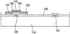
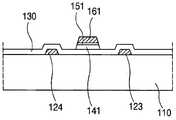
도 3은 본 발명의 실시예에 따른 액정 표시 장치용 어레이 기판의 평면도를 도시한 것이고, 도 4와 도 5는 도 3에서 각각 Ⅳ-Ⅳ선 및 Ⅴ-Ⅴ선을 따라 자른 단면을 도시한 것이다.3 is a plan view of an array substrate for a liquid crystal display according to an exemplary embodiment of the present invention, and FIGS. 4 and 5 are cross-sectional views taken along lines IV-IV and V-V in FIG. 3, respectively. .
도 3과 도 4 및 도 5에 도시한 바와 같이, 투명한 절연 기판(110) 위에 가로 방향의 게이트 배선(121)과 게이트 배선(121)의 분지인 게이트 전극(122), 그리고 게이트 배선(121)에서 세로 방향으로 연장된 제 1 차광 패턴(123) 및 제 1 차광 패턴(123)과 일정 간격으로 이격되어 있는 세로 방향의 제 2 차광 패턴(124)이 형성 되어 있다.3, 4, and 5, the
다음, 게이트 배선(121)과 게이트 전극(122), 제 1 및 제 2 차광 패턴(123, 124) 위에 게이트 절연막(130) 형성되어 이들을 덮고 있다.Next, a
게이트 절연막(130) 상부에는 비정질 실리콘으로 이루어진 액티브층(141)과 불순물이 도핑된 비정질 실리콘으로 이루어진 오믹 콘택층(151, 152)이 차례로 형성되어 있다.An
오믹 콘택층(151, 152) 상부에는 세로 방향의 데이터 배선(161)이 형성되어 있는데, 데이터 배선(161)은 게이트 배선(121)과 교차함으로써 화소 영역을 정의하며, 데이터 배선(161)에서 연장된 소스 전극(162)과 소스 전극(162) 맞은 편에 형성되어 있는 드레인 전극(163)은 게이트 전극(122)을 중심으로 마주 대하고 있다.The
오믹 콘택층(151, 152)은 데이터 배선(161), 소스 전극(162), 그리고 드레인 전극(163)과 같은 모양을 가지며, 액티브층(141)은 소스 및 드레인 전극(162, 163) 사이의 채널 부분을 제외하고 데이터 배선(161), 소스 전극(162) 및 드레인 전극(163)과 동일한 모양을 가진다.The ohmic contact layers 151 and 152 have the same shape as the
데이터 배선(161)과 소스 및 드레인 전극(162, 163) 상부에는 실리콘 질화막이나 실리콘 산화막 또는 유기 절연막으로 이루어진 보호층(170)이 형성되어 있고, 보호층(170)은 드레인 전극(163)을 일부 드러내는 콘택홀(171)을 가진다.A
보호층(170) 상부의 화소 영역에는 투명한 도전 물질로 이루어진 화소 전극(181)이 형성되어 있는데, 화소 전극은 콘택홀(171)을 통해 드레인 전극(163)과 접촉하고, 전단 게이트 배선(121)과 일부 중첩하여 스토리지 캐패시터를 형성한 다. 이때, 게이트 배선(121) 상부에 데이터 배선(161)과 같은 물질로 화소 전극(181)과 연결된 패턴을 형성함으로써, 스토리지 캐패시터를 형성할 수도 있다. 또한, 화소 전극(181)은 제 1 및 제 2 차광 패턴(123, 124)과도 일부 중첩되어 있다.A
일반적으로 상부의 블랙 매트릭스(도시하지 않음)와 화소 전극(181)은 합착마진을 고려하여 5 ㎛ 정도 중첩되도록 형성하는데, 본 발명에서 제 1 및 제 2 차광 패턴(123, 124)이 화소 전극(181)과 중첩되지 않는 부분의 폭은 2 ㎛ 정도이다. 따라서, 합착마진이 7 ㎛ 정도로 종래에 비해 증가되어, 상부 기판과 하부 기판의 크기 변화가 다르더라도 빛샘을 방지할 수 있다.In general, the upper black matrix (not shown) and the
또한, 제 1 차광 패턴(123)은 게이트 배선(121)과 연결되어 있어 캐패시터를 형성하므로, 스토리지 캐패시터의 용량이 증가된다.In addition, since the first
한편, 최근 액정 표시 장치의 대형화 및 고정세화에 따라 배선의 길이가 길어지고 폭은 줄어들게 되었다. 이에 따라 배선이 단선될 확률이 높아지게 되었는데, 데이터 배선(161)이 단선될 경우 선결함(line defect)과 같은 불량이 발생한다.On the other hand, in recent years, as the size and size of liquid crystal display devices have increased, the length of the wiring has become longer and the width thereof has decreased. As a result, the probability of disconnection of the wire increases, and when the
여기서, 제 2 차광 패턴(123)의 상부와 하부는 연장되어 데이터 배선(161)과 중첩하도록 되어 있는데, 데이터 배선(161)이 단선될 경우 이 부분을 단락시켜 데이터 배선(161)의 단선을 수리할 수 있다.Here, the upper and lower portions of the second
한편, 일반적인 액정 표시 장치에서 화소 전극(181)과 데이터 배선(161)은 보통 3 ㎛ 정도의 간격을 가지고 떨어져 있는데, 이러한 경우 화소 전극(181)과 데 이터 배선(161) 사이의 기생 용량에 의해 커플링(coupling)이 발생할 수 있다. 그러나, 본 발명에서는 차광 패턴(123, 124)과 중첩된 범위 내에서 화소 전극(181)의 폭을 줄임으로써 화소 전극(181)과 데이터 배선(161) 사이의 거리가 멀어지게 하여 화소 전극(181)과 데이터 배선(161) 사이의 기생 용량를 감소시킬 수도 있다. 따라서, 액정 표시 장치의 화질을 향상시킬 수 있다.Meanwhile, in a typical liquid crystal display device, the
이러한 액정 표시 장치용 어레이 기판의 제조 방법에 대하여 도 6a 내지 도 6d와 도 7a 내지 도 7d를 참조하여 상세히 설명한다.A method of manufacturing the array substrate for a liquid crystal display device will be described in detail with reference to FIGS. 6A to 6D and 7A to 7D.
도 6a 내지 도 6d는 도 3에서 Ⅳ-Ⅳ선에 해당하는 단면도이고, 도 7a 내지 도 7d는 도 3의 Ⅴ-Ⅴ선에 해당하는 단면도이다.6A to 6D are cross-sectional views corresponding to line IV-IV in FIG. 3, and FIGS. 7A to 7D are cross-sectional views corresponding to line V-V in FIG. 3.
먼저, 도 6a 및 도 7a에 도시한 바와 같이 유리와 같은 투명한 기판(110) 위에 금속 물질을 스퍼터링과 같은 방법으로 증착하고 제 1 마스크를 이용한 사진 식각 공정으로 패터닝하여 가로 방향의 게이트 배선(121)과 게이트 배선(121)의 분지인 게이트 전극(122), 그리고 게이트 배선(121)에서 세로 방향으로 연장된 제 1 차광 패턴(123) 및 제 1 차광 패턴(123)과 일정 간격 이격된 세로 방향의 제 2 차광 패턴(124)을 형성한다.First, as illustrated in FIGS. 6A and 7A, a metal material is deposited on a
여기서, 게이트 배선(121)은 비저항이 작고 기판(110)과의 접착력이 좋은 물질로 형성하는 것이 좋다.Here, the
다음, 도 6b 및 도 7b에 도시한 바와 같이 실리콘 질화막이나 실리콘 산화막(130), 비정질 실리콘막, 불순물로 도핑된 비정질 실리콘막을 차례로 증착한 후, 금속층을 스퍼터링 방법으로 증착한다. 이어, 제 2 마스크를 이용하여 금속층 과 불순물 비정질 실리콘막, 비정질 실리콘막을 순차적으로 패터닝함으로써 데이터 배선(161)과 소스 및 드레인 전극(162, 163), 오믹 콘택층(151, 152), 그리고 액티브층(141)을 형성한다.Next, as illustrated in FIGS. 6B and 7B, a silicon nitride film, a
이때 사용되는 제 2 마스크는 빛의 투과 영역이 다른 세 부분을 포함하는데, 이러한 제 2 마스크를 도 8에 도시하였다.In this case, the second mask used includes three parts having different light transmitting regions, and the second mask is illustrated in FIG. 8.
도시한 바와 같이, 투명한 기판(210) 위에 빛을 차단하기 위한 막이 형성되어 있어, 데이터 배선(161)과 소스 및 드레인 전극(162, 163)에 대응하는 부분(A)에서는 빛이 투과되지 않으며, 소스 및 드레인 전극(162, 163) 사이의 채널에 대응하는 부분(B)은 빛이 일부만 투과되고, 나머지 부분(C)은 빛이 모두 투과된다. B 부분에는 슬릿과 같은 미세한 패턴이 형성되어 있어, 빛의 회절 현상에 의해 빛의 투과도가 C 부분보다 작게 된다.As shown, a film for blocking light is formed on the
이러한 마스크를 이용하여 금속층 상부에 두께가 다른 감광막 패턴을 형성하고 식각 공정을 실시함으로써, 한 번의 식각 공정으로 데이터 배선(161)과 소스 및 드레인 전극(162, 163), 오믹 콘택층(151, 152), 그리고 액티브층(141)을 형성할 수 있다.By using such a mask to form a photoresist pattern having a different thickness on the metal layer and performing an etching process, the data wiring 161, the source and drain
다음, 도 6c 및 도 7c에 도시한 바와 같이 실리콘 질화막이나 실리콘 산화막, 유기 절연막을 증착 또는 도포하여 보호층(170)을 형성하고, 제 3 마스크를 이용한 사진 식각 공정으로 보호층(170)을 패터닝하여 드레인 전극(163) 상부에 콘택홀(171)을 형성한다.Next, as illustrated in FIGS. 6C and 7C, the
다음, 도 6d 및 도 7d에 도시한 바와 같이 인듐-틴-옥사이드(indium-tin- oxide ; ITO)나 인듐-징크-옥사이드(indium-zinc-oxide ; IZO)와 같은 물질을 증착하고, 제 4 마스크를 이용하여 패터닝함으로써 화소 전극(181)을 형성한다. 화소 전극(181)은 콘택홀(171)을 통해 드레인 전극(162)과 연결되며, 전단 게이트 배선(121), 그리고 제 1 및 제 2 차광 패턴(123, 124)과 일부 중첩한다.Next, as shown in FIGS. 6D and 7D, a material such as indium-tin-oxide (ITO) or indium-zinc-oxide (IZO) is deposited, and the fourth layer is deposited. The
이와 같이, 본 발명에 따른 액정 표시 장치용 어레이 기판은 4장의 마스크를 이용하여 제작되므로, 5장의 마스크를 이용한 종래의 어레이 기판보다 제조 공정 및 제조 비용을 감소시킬 수 있다.As described above, since the array substrate for the liquid crystal display device according to the present invention is manufactured using four masks, the manufacturing process and the manufacturing cost can be reduced compared to the conventional array substrate using the five masks.
본 발명은 상기한 실시예에 한정되지 아니하며, 본 발명의 정신을 벗어나지 않는 이상 다양한 변화와 변형이 가능하다.
The present invention is not limited to the above embodiments, and various changes and modifications can be made without departing from the spirit of the present invention.
본 발명에 따른 액정 표시 장치는 4장의 마스크를 이용하여 제조함으로써 제조 비용을 절감할 수 있으며, 게이트 배선과 같은 물질로 화소 전극과 일부 중첩하는 제 1 및 제 2 차광 패턴을 형성함으로써 공정 마진을 향상시켜 빛샘 불량을 방지할 수 있다. 또한, 어느 하나의 차광 패턴은 게이트 배선과 연결되도록 하여 스토리지 캐패시터의 용량을 향상시키며, 나머지 하나의 차광 패턴은 데이터 배선과 일부 중첩되도록 함으로써 데이터 배선이 단선될 경우, 데이터 배선과 차광 패턴을 단락시켜 단선을 수리할 수 있다.The liquid crystal display according to the present invention can reduce manufacturing costs by manufacturing using four masks, and improves process margins by forming first and second light blocking patterns partially overlapping the pixel electrodes with a material such as a gate wiring. It can prevent light leakage defect. In addition, one of the light blocking patterns is connected to the gate wiring to improve the capacity of the storage capacitor, and the other light blocking pattern is partially overlapped with the data wiring so that when the data wiring is disconnected, the data wiring and the light blocking pattern are shorted. The disconnection can be repaired.
한편, 차광 패턴과 화소 전극의 중첩된 폭 내에서 화소 전극의 면적을 감소시킴으로써 데이터 배선과 화소 전극 사이의 거리를 멀게 하여 화소 전극과 데이터 배선 사이의 기생 용량을 감소시킬 수 있다. 따라서, 얼룩을 개선하고 화질을 향상시킬 수 있다.On the other hand, by reducing the area of the pixel electrode within the overlapping width of the light blocking pattern and the pixel electrode, the distance between the data line and the pixel electrode can be increased to reduce the parasitic capacitance between the pixel electrode and the data line. Therefore, it is possible to improve spots and to improve image quality.
Claims (7)
Translated fromKoreanPriority Applications (1)
| Application Number | Priority Date | Filing Date | Title |
|---|---|---|---|
| KR1020000085414AKR100650400B1 (en) | 2000-12-29 | 2000-12-29 | Array substrate for liquid crystal display device and manufacturing method thereof |
Applications Claiming Priority (1)
| Application Number | Priority Date | Filing Date | Title |
|---|---|---|---|
| KR1020000085414AKR100650400B1 (en) | 2000-12-29 | 2000-12-29 | Array substrate for liquid crystal display device and manufacturing method thereof |
Publications (2)
| Publication Number | Publication Date |
|---|---|
| KR20020056110A KR20020056110A (en) | 2002-07-10 |
| KR100650400B1true KR100650400B1 (en) | 2006-11-27 |
Family
ID=27688619
Family Applications (1)
| Application Number | Title | Priority Date | Filing Date |
|---|---|---|---|
| KR1020000085414AExpired - Fee RelatedKR100650400B1 (en) | 2000-12-29 | 2000-12-29 | Array substrate for liquid crystal display device and manufacturing method thereof |
Country Status (1)
| Country | Link |
|---|---|
| KR (1) | KR100650400B1 (en) |
Families Citing this family (6)
| Publication number | Priority date | Publication date | Assignee | Title |
|---|---|---|---|---|
| KR100473226B1 (en)* | 2002-07-11 | 2005-03-10 | 엘지.필립스 엘시디 주식회사 | Active Matrix type Organic Light Emitting Diode Device |
| KR100905472B1 (en) | 2002-12-17 | 2009-07-02 | 삼성전자주식회사 | Thin film transistor array substrate and liquid crystal display including the same |
| KR100980011B1 (en)* | 2003-07-23 | 2010-09-03 | 삼성전자주식회사 | Thin film transistor array panel for multidomain liquid crystal display |
| KR101113065B1 (en)* | 2005-04-29 | 2012-02-15 | 엘지디스플레이 주식회사 | Optical mask for liquid crystal display |
| KR101236509B1 (en)* | 2005-12-26 | 2013-02-21 | 엘지디스플레이 주식회사 | Liquid crystal display and method for repairing the same |
| KR101419224B1 (en)* | 2007-09-04 | 2014-07-16 | 엘지디스플레이 주식회사 | Thin film transistor array substrate for liquid crystal display apparatus and manufacturing method thereof |
- 2000
- 2000-12-29KRKR1020000085414Apatent/KR100650400B1/ennot_activeExpired - Fee Related
Also Published As
| Publication number | Publication date |
|---|---|
| KR20020056110A (en) | 2002-07-10 |
Similar Documents
| Publication | Publication Date | Title |
|---|---|---|
| KR100391157B1 (en) | array panel of liquid crystal display and manufacturing method thereof | |
| KR100808466B1 (en) | Array substrate for liquid crystal display device and manufacturing method thereof | |
| US20030136971A1 (en) | Thin film transistor array panel for display and manufacturing method thereof | |
| KR100207136B1 (en) | Electrode substrate, its manufacturing method and display device using same | |
| US20110273648A1 (en) | Liquid crystal display device and method of fabricating the same | |
| KR20030010023A (en) | array panel of liquid crystal display and manufacturing method of the same | |
| KR101383703B1 (en) | Thin film transistor array panel and manufacturung method thereof | |
| KR100650401B1 (en) | array panel of liquid crystal display and manufacturing method thereof | |
| US7214965B2 (en) | Thin film transistor array panel and method of manufacturing the same | |
| US20050024622A1 (en) | Exposure mask and method for divisional exposure | |
| KR100345959B1 (en) | Thin film transistor array panel for liquid crystal display and manufacturing method of the same | |
| KR100650400B1 (en) | Array substrate for liquid crystal display device and manufacturing method thereof | |
| KR20020011573A (en) | liquid crystal display and fabricating method of the same | |
| KR100848108B1 (en) | liquid crystal display, thin film transistor array plate and method for fabricating the plate | |
| KR100924751B1 (en) | LCD and its manufacturing method | |
| KR100386458B1 (en) | array panel of liquid crystal display and manufacturing method thereof | |
| KR100413512B1 (en) | an array panel for liquid crystal display and manufacturing method thereof | |
| US8435722B2 (en) | Method for fabricating liquid crystal display device | |
| KR100648422B1 (en) | Array substrate for liquid crystal display device and manufacturing method thereof | |
| JPH11295760A (en) | Array substrate for display device and method of manufacturing the same | |
| KR100529574B1 (en) | Planar drive type liquid crystal display device and manufacturing method thereof | |
| KR100268105B1 (en) | Thin Film Transistor Board and Manufacturing Method | |
| KR100694576B1 (en) | Array substrate for liquid crystal display device and manufacturing method thereof | |
| KR20020056111A (en) | array panel of liquid crystal display and manufacturing method thereof | |
| KR101408687B1 (en) | An Array Substrate of Liquid Crystal Display Device and the method for fabricating thereof |
Legal Events
| Date | Code | Title | Description |
|---|---|---|---|
| PA0109 | Patent application | St.27 status event code:A-0-1-A10-A12-nap-PA0109 | |
| PN2301 | Change of applicant | St.27 status event code:A-3-3-R10-R13-asn-PN2301 St.27 status event code:A-3-3-R10-R11-asn-PN2301 | |
| PG1501 | Laying open of application | St.27 status event code:A-1-1-Q10-Q12-nap-PG1501 | |
| A201 | Request for examination | ||
| PA0201 | Request for examination | St.27 status event code:A-1-2-D10-D11-exm-PA0201 | |
| R17-X000 | Change to representative recorded | St.27 status event code:A-3-3-R10-R17-oth-X000 | |
| E701 | Decision to grant or registration of patent right | ||
| PE0701 | Decision of registration | St.27 status event code:A-1-2-D10-D22-exm-PE0701 | |
| GRNT | Written decision to grant | ||
| PR0701 | Registration of establishment | St.27 status event code:A-2-4-F10-F11-exm-PR0701 | |
| PR1002 | Payment of registration fee | St.27 status event code:A-2-2-U10-U11-oth-PR1002 Fee payment year number:1 | |
| PG1601 | Publication of registration | St.27 status event code:A-4-4-Q10-Q13-nap-PG1601 | |
| PN2301 | Change of applicant | St.27 status event code:A-5-5-R10-R13-asn-PN2301 St.27 status event code:A-5-5-R10-R11-asn-PN2301 | |
| PR1001 | Payment of annual fee | St.27 status event code:A-4-4-U10-U11-oth-PR1001 Fee payment year number:4 | |
| PR1001 | Payment of annual fee | St.27 status event code:A-4-4-U10-U11-oth-PR1001 Fee payment year number:5 | |
| R18-X000 | Changes to party contact information recorded | St.27 status event code:A-5-5-R10-R18-oth-X000 | |
| PR1001 | Payment of annual fee | St.27 status event code:A-4-4-U10-U11-oth-PR1001 Fee payment year number:6 | |
| R18-X000 | Changes to party contact information recorded | St.27 status event code:A-5-5-R10-R18-oth-X000 | |
| R18-X000 | Changes to party contact information recorded | St.27 status event code:A-5-5-R10-R18-oth-X000 | |
| FPAY | Annual fee payment | Payment date:20120928 Year of fee payment:7 | |
| PR1001 | Payment of annual fee | St.27 status event code:A-4-4-U10-U11-oth-PR1001 Fee payment year number:7 | |
| FPAY | Annual fee payment | Payment date:20130930 Year of fee payment:8 | |
| PR1001 | Payment of annual fee | St.27 status event code:A-4-4-U10-U11-oth-PR1001 Fee payment year number:8 | |
| FPAY | Annual fee payment | Payment date:20141021 Year of fee payment:9 | |
| PR1001 | Payment of annual fee | St.27 status event code:A-4-4-U10-U11-oth-PR1001 Fee payment year number:9 | |
| FPAY | Annual fee payment | Payment date:20151028 Year of fee payment:10 | |
| PR1001 | Payment of annual fee | St.27 status event code:A-4-4-U10-U11-oth-PR1001 Fee payment year number:10 | |
| FPAY | Annual fee payment | Payment date:20161012 Year of fee payment:11 | |
| PR1001 | Payment of annual fee | St.27 status event code:A-4-4-U10-U11-oth-PR1001 Fee payment year number:11 | |
| P22-X000 | Classification modified | St.27 status event code:A-4-4-P10-P22-nap-X000 | |
| FPAY | Annual fee payment | Payment date:20171016 Year of fee payment:12 | |
| PR1001 | Payment of annual fee | St.27 status event code:A-4-4-U10-U11-oth-PR1001 Fee payment year number:12 | |
| FPAY | Annual fee payment | Payment date:20181015 Year of fee payment:13 | |
| PR1001 | Payment of annual fee | St.27 status event code:A-4-4-U10-U11-oth-PR1001 Fee payment year number:13 | |
| PC1903 | Unpaid annual fee | St.27 status event code:A-4-4-U10-U13-oth-PC1903 Not in force date:20191122 Payment event data comment text:Termination Category : DEFAULT_OF_REGISTRATION_FEE | |
| PC1903 | Unpaid annual fee | St.27 status event code:N-4-6-H10-H13-oth-PC1903 Ip right cessation event data comment text:Termination Category : DEFAULT_OF_REGISTRATION_FEE Not in force date:20191122 |