KR100649754B1 - Semiconductor device package - Google Patents
Semiconductor device packageDownload PDFInfo
- Publication number
- KR100649754B1 KR100649754B1KR1020050103203AKR20050103203AKR100649754B1KR 100649754 B1KR100649754 B1KR 100649754B1KR 1020050103203 AKR1020050103203 AKR 1020050103203AKR 20050103203 AKR20050103203 AKR 20050103203AKR 100649754 B1KR100649754 B1KR 100649754B1
- Authority
- KR
- South Korea
- Prior art keywords
- fiber
- semiconductor device
- package
- substrate
- package substrate
- Prior art date
- Legal status (The legal status is an assumption and is not a legal conclusion. Google has not performed a legal analysis and makes no representation as to the accuracy of the status listed.)
- Expired - Fee Related
Links
Images


Classifications
- H—ELECTRICITY
- H01—ELECTRIC ELEMENTS
- H01L—SEMICONDUCTOR DEVICES NOT COVERED BY CLASS H10
- H01L23/00—Details of semiconductor or other solid state devices
- H01L23/02—Containers; Seals
- H—ELECTRICITY
- H10—SEMICONDUCTOR DEVICES; ELECTRIC SOLID-STATE DEVICES NOT OTHERWISE PROVIDED FOR
- H10H—INORGANIC LIGHT-EMITTING SEMICONDUCTOR DEVICES HAVING POTENTIAL BARRIERS
- H10H20/00—Individual inorganic light-emitting semiconductor devices having potential barriers, e.g. light-emitting diodes [LED]
- H10H20/80—Constructional details
- H10H20/85—Packages
- H10H20/858—Means for heat extraction or cooling
- H10H20/8581—Means for heat extraction or cooling characterised by their material
- H—ELECTRICITY
- H01—ELECTRIC ELEMENTS
- H01L—SEMICONDUCTOR DEVICES NOT COVERED BY CLASS H10
- H01L2224/00—Indexing scheme for arrangements for connecting or disconnecting semiconductor or solid-state bodies and methods related thereto as covered by H01L24/00
- H01L2224/01—Means for bonding being attached to, or being formed on, the surface to be connected, e.g. chip-to-package, die-attach, "first-level" interconnects; Manufacturing methods related thereto
- H01L2224/42—Wire connectors; Manufacturing methods related thereto
- H01L2224/47—Structure, shape, material or disposition of the wire connectors after the connecting process
- H01L2224/48—Structure, shape, material or disposition of the wire connectors after the connecting process of an individual wire connector
- H01L2224/4805—Shape
- H01L2224/4809—Loop shape
- H01L2224/48091—Arched
- H—ELECTRICITY
- H01—ELECTRIC ELEMENTS
- H01L—SEMICONDUCTOR DEVICES NOT COVERED BY CLASS H10
- H01L2224/00—Indexing scheme for arrangements for connecting or disconnecting semiconductor or solid-state bodies and methods related thereto as covered by H01L24/00
- H01L2224/01—Means for bonding being attached to, or being formed on, the surface to be connected, e.g. chip-to-package, die-attach, "first-level" interconnects; Manufacturing methods related thereto
- H01L2224/42—Wire connectors; Manufacturing methods related thereto
- H01L2224/47—Structure, shape, material or disposition of the wire connectors after the connecting process
- H01L2224/49—Structure, shape, material or disposition of the wire connectors after the connecting process of a plurality of wire connectors
- H01L2224/491—Disposition
- H01L2224/49105—Connecting at different heights
- H01L2224/49107—Connecting at different heights on the semiconductor or solid-state body
- H—ELECTRICITY
- H01—ELECTRIC ELEMENTS
- H01L—SEMICONDUCTOR DEVICES NOT COVERED BY CLASS H10
- H01L2224/00—Indexing scheme for arrangements for connecting or disconnecting semiconductor or solid-state bodies and methods related thereto as covered by H01L24/00
- H01L2224/73—Means for bonding being of different types provided for in two or more of groups H01L2224/10, H01L2224/18, H01L2224/26, H01L2224/34, H01L2224/42, H01L2224/50, H01L2224/63, H01L2224/71
- H01L2224/732—Location after the connecting process
- H01L2224/73251—Location after the connecting process on different surfaces
- H01L2224/73265—Layer and wire connectors
- H—ELECTRICITY
- H01—ELECTRIC ELEMENTS
- H01L—SEMICONDUCTOR DEVICES NOT COVERED BY CLASS H10
- H01L2924/00—Indexing scheme for arrangements or methods for connecting or disconnecting semiconductor or solid-state bodies as covered by H01L24/00
- H01L2924/10—Details of semiconductor or other solid state devices to be connected
- H01L2924/11—Device type
- H01L2924/12—Passive devices, e.g. 2 terminal devices
- H01L2924/1204—Optical Diode
- H01L2924/12041—LED
- H—ELECTRICITY
- H01—ELECTRIC ELEMENTS
- H01S—DEVICES USING THE PROCESS OF LIGHT AMPLIFICATION BY STIMULATED EMISSION OF RADIATION [LASER] TO AMPLIFY OR GENERATE LIGHT; DEVICES USING STIMULATED EMISSION OF ELECTROMAGNETIC RADIATION IN WAVE RANGES OTHER THAN OPTICAL
- H01S5/00—Semiconductor lasers
- H01S5/02—Structural details or components not essential to laser action
- H01S5/022—Mountings; Housings
- H01S5/0233—Mounting configuration of laser chips
- H01S5/02345—Wire-bonding
- H—ELECTRICITY
- H01—ELECTRIC ELEMENTS
- H01S—DEVICES USING THE PROCESS OF LIGHT AMPLIFICATION BY STIMULATED EMISSION OF RADIATION [LASER] TO AMPLIFY OR GENERATE LIGHT; DEVICES USING STIMULATED EMISSION OF ELECTROMAGNETIC RADIATION IN WAVE RANGES OTHER THAN OPTICAL
- H01S5/00—Semiconductor lasers
- H01S5/02—Structural details or components not essential to laser action
- H01S5/024—Arrangements for thermal management
- H01S5/02476—Heat spreaders, i.e. improving heat flow between laser chip and heat dissipating elements
Landscapes
- Physics & Mathematics (AREA)
- Condensed Matter Physics & Semiconductors (AREA)
- General Physics & Mathematics (AREA)
- Engineering & Computer Science (AREA)
- Computer Hardware Design (AREA)
- Microelectronics & Electronic Packaging (AREA)
- Power Engineering (AREA)
- Cooling Or The Like Of Semiconductors Or Solid State Devices (AREA)
- Semiconductor Lasers (AREA)
- Led Device Packages (AREA)
Abstract
Translated fromKoreanDescription
Translated fromKorean도1은 종래의 반도체 발광소자 패키지 구조를 나타내는 측단면도이다.1 is a side sectional view showing a conventional semiconductor light emitting device package structure.
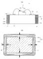
도2a 및 도2b는 각각 본 발명의 일실시형태에 따른 반도체 소자 패키지 구조를 나타내는 측단면도 및 평면도(X-X'방향으로 절개한 면)이다.2A and 2B are side cross-sectional views and plan views (surfaces cut in the X-X 'direction), respectively, illustrating a semiconductor device package structure according to one embodiment of the present invention.
도3는 도2a의 패키지 기판을 Y-Y'방향으로 절개하여 본 단면도이다.3 is a cross-sectional view of the package substrate of FIG. 2A taken along the line Y-Y '.
도4a 및 도4b는 섬유강화 폴리머 복합체의 채용여부에 따른 반도체 소자에 인가되는 열응력의 차이를 나타내는 시뮬레이션 결과이다.4A and 4B are simulation results showing a difference in thermal stress applied to a semiconductor device depending on whether a fiber-reinforced polymer composite is employed.
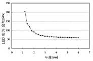
도5는 섬유강화 폴리머 복합체의 두께에 따른 반도체 소자에 인가되는 응력변화를 나타내는 그래프이다.5 is a graph showing the stress change applied to the semiconductor device according to the thickness of the fiber-reinforced polymer composite.
<도면의 주요부분에 대한 부호설명><Code Description of Main Parts of Drawing>
25: 반도체 소자 27:패키지기판25: semiconductor element 27: package substrate
29: 섬유강화 폴리머 복합체29a: 탄소 섬유29: fiber-reinforced
29b: 수지부29b: resin part
본 발명은 반도체 소자 패키지에 관한 것으로서, 보다 상세하게는 발열원으로 작용하는 반도체 소자와 열싱크로 작용하는 패키지 기판 사이에 발생되는 열응력을 억제하고, 열방출특성을 향상시킬 수 있는 새로운 반도체 소자 패키지에 관한 것이다.The present invention relates to a semiconductor device package, and more particularly, to a new semiconductor device package capable of suppressing thermal stress generated between a semiconductor device serving as a heat generating source and a package substrate serving as a heat sink and improving heat dissipation characteristics. It is about.
일반적으로, 발광다이오드 또는 레이저 다이오드 등을 위한 반도체 소자 패키지는 반도체 소자에서 발생되는 열이 효과적으로 방출되도록 설계되고 제조된다. 특히, 조명분야에서 사용되는 고출력 발광다이오드 패키지는 발열량이 매우 크므로, 상기한 열방출특성이 매우 중요하게 요구된다.In general, semiconductor device packages for light emitting diodes, laser diodes, and the like are designed and manufactured to effectively release heat generated from semiconductor devices. In particular, the high output light emitting diode package used in the lighting field is very large heat generation, so the heat dissipation characteristics are very important.
이러한 열방출특성을 향상시키기 위해 일반적으로 채용되는 방식은 반도체 소자를 구성하는 물질보다 높은 열전도성을 갖는 물질로 이루어진 패키지 기판을 사용하는 것이다. 간단한 일예로서 도1에는 발광다이오드 패키지가 도시되어 있다.A method generally employed to improve the heat dissipation characteristics is to use a package substrate made of a material having a higher thermal conductivity than the material constituting the semiconductor device. As a simple example, FIG. 1 shows a light emitting diode package.
도1과 같이, 종래의 발광다이오드 패키지(10)는 패키지 기판(17)과 그 상면에 실장된 발광다이오드칩(15)을 포함한다. 상기 발광다이오드는 기판(11) 상에 순차적으로 형성된 제1 도전형 반도체층(12), 활성층(13) 및 제2 도전형 활성층(14)을 포함하며, 상기 제1 및 제2 도전형 반도체층(12,14)에 각각 접속된 제1 및 제2 전극(16a,16b)은 와이어에 의해 상기 패키지 기판(17) 상에 제1 및 제2 본딩패드(18a,18b)에 연결된다.As shown in FIG. 1, the
상기 패키지 기판(17)은 실리콘과 같은 반도체기판, 세라믹기판 및 금속기판 과 같이, 발광다이오드(15)의 구성물질보다 열전도성이 우수한 물질로 이루어지며, 이로써 발광다이오드(15)로부터 발생된 열을 방출시킬 수 있다(점선 화살표로 표시됨).The
하지만, 열전도성이 높은 패키지 기판(17)은 발광다이오드(15)의 구성물질에 비해 열팽창계수가 크므로, 발광다이오드 부착공정 또는 구동과정에서 열에 의해 노출된 후에 냉각될 때에, 상기 발광다이오드(15)과 상기 패키지 기판(17)의 계면에서 화살표로 표시된 바와 같이 큰 열응력이 발생된다. 이러한 열응력로 인해, 발광다이오드(15)의 신뢰성을 저하시키거나, 심한 경우에는 발광다이오드(15)에 크랙이 발생되어 불량을 초래할 수 있다.However, the thermally
이와 같이, 계면에서 발생된 열응력을 완화하기 위해서, 종래에는 도1에 도시된 바와 같이 발광다이오드(15)과 패키지 기판(17) 사이에 완충재료층(L)을 채용하였다. 이러한 완충재료층(L)은 열응력을 완화시키는 수단으로서 바람직하지만, 열전달경로에 형성되므로, 오히려 패키지 기판에 의한 열방출기능을 저하시키는 문제가 있다.As described above, in order to alleviate the thermal stress generated at the interface, a buffer layer L is employed between the
본 발명은 상술된 종래 기술의 문제를 해결하기 위한 것으로서, 그 목적은 섬유강화 폴리머 복합체를 이용하여 패키지 기판의 열팽창을 억제함으로써 반도체 소자와 계면에서 발생되는 열응력을 감소시킬 수 있는 반도체 소자 패키지를 제공하는데 있다.The present invention is to solve the above-mentioned problems of the prior art, an object of the present invention is to provide a semiconductor device package that can reduce the thermal stress generated at the interface with the semiconductor device by inhibiting thermal expansion of the package substrate using a fiber-reinforced polymer composite To provide.
상기한 기술적 과제를 달성하기 위해서, 본 발명은In order to achieve the above technical problem, the present invention
발열원으로 작용하는 반도체 소자와, 상면에 상기 반도체 소자가 실장되며, 적어도 상기 반도체 소자보다 높은 열전도성을 갖는 패키지 기판과, 상기 패키지 기판의 측면을 둘러싸도록 형성되며, 강화재로 작용하는 섬유와 상기 섬유를 내부에 포함하는 수지부로 구성된 섬유강화 폴리머 복합체를 포함하는 반도체 소자 패키지를 제공한다.A semiconductor device serving as a heat generating source, a semiconductor substrate mounted on an upper surface of the semiconductor device, the package substrate having a higher thermal conductivity than at least the semiconductor device, and surrounding the side surface of the package substrate, the fibers serving as a reinforcing material, and the fibers It provides a semiconductor device package comprising a fiber-reinforced polymer composite composed of a resin portion containing therein.
바람직하게, 상기 섬유강화 폴리머 복합체에 포함된 섬유는 전체 복합체 부피 중 30% 내지 80%에 해당한다.Preferably, the fiber included in the fiber reinforced polymer composite corresponds to 30% to 80% of the total composite volume.
또한, 상기 섬유로는 이에 한정되지 않으나, 탄소, 흑연 또는 유리 섬유일 수 있으며, 특히 열방출기능을 부가하기 위해서 열전도성이 우수한 탄소 섬유 또는 흑연 섬유가 보다 바람직하게 사용될 수 있다. 상기 수지부는 에폭시계 수지, 실리콘계 수지, 폴리에스테르계 수지 또는 비닐에스테르계 수지로 이루어질 수 있다.In addition, the fiber is not limited thereto, and may be carbon, graphite, or glass fiber, and particularly, carbon fiber or graphite fiber having excellent thermal conductivity may be more preferably used in order to add a heat release function. The resin part may be made of an epoxy resin, a silicone resin, a polyester resin, or a vinyl ester resin.
바람직하게, 상기 섬유강화 폴리머 복합체의 상기 섬유는 상기 패키지 기판의 측면을 따라 권선될 수 있다. 내부 섬유가 권선된 형태를 갖는 섬유강화 폴리머 복합체는 열팽창시에 내부방향으로 팽창된 정도가 강화되어 패키지 기판의 열팽창을 보다 효과적으로 억제시킬 수 있다. 상기 섬유는 상기 패키지 기판의 상면 또는 하면을 기준으로 일정한 각을 갖도록 경사진 형태로 권선된 것이 바람직하다. 열전도성이 보다 우수한 섬유를 통해 패키지 기판 상면에 위치한 반도체 소자의 열을 효과적으로 방출시킬 수 있다.Preferably, the fibers of the fiber reinforced polymer composite may be wound along the side of the package substrate. The fiber-reinforced polymer composite having a form in which the inner fiber is wound can be more expanded inwardly during thermal expansion to more effectively suppress thermal expansion of the package substrate. The fiber is preferably wound in an inclined form to have a constant angle with respect to the upper or lower surface of the package substrate. The more thermally conductive fibers can effectively release the heat of the semiconductor device located on the package substrate.
상기 패키지 기판은 반도체 기판, 세라믹 기판 또는 금속 기판일 수 있으며,본 발명은 발열량이 큰 발광다이오드 칩 또는 레이저 다이오드 칩을 포함한 패키지에 유용하게 적용될 수 있다.The package substrate may be a semiconductor substrate, a ceramic substrate, or a metal substrate, and the present invention may be usefully applied to a package including a light emitting diode chip or a laser diode chip having a high heat generation amount.
이하, 첨부된 도면을 참조하여 본 발명을 보다 상세히 설명한다.Hereinafter, with reference to the accompanying drawings will be described the present invention in more detail.
도2a 및 도2b는 각각 본 발명의 일실시형태에 따른 반도체 소자 패키지 구조를 나타내는 측단면도 및 평면도(X-X'방향으로 절개한 면)이다.2A and 2B are side cross-sectional views and plan views (surfaces cut in the X-X 'direction), respectively, illustrating a semiconductor device package structure according to one embodiment of the present invention.
우선, 도2a를 참조하면, 본 실시형태에 따른 발광다이오드 패키지(20)는 패키지 기판(27)과 그 상면에 실장된 반도체 소자(25)를 포함한다.First, referring to FIG. 2A, the light
상기 반도체 소자(25)는 도1과 유사한 발광다이오드로 도시되어 있으나, 이에 한정되지 않으며, 레이저 다이오드와 같이 발열량이 큰 다른 반도체 소자일 수 있다.The
상기 패키지 기판(27)은 반도체 소자(25)에 비해 높은 열전도성을 갖는 물질 로 이루어질 수 있으며, 이에 한정되지 않으나, 실리콘과 같은 반도체 기판, 세라믹 기판 또는 금속 기판일 수 있다. 또한, 상기 패키지 기판(27)은 반도체소자(25)의 두 전극(26a,26b)에 각각 접속되는 본딩패드(28a,28b)와 같은 적절한 배선구조를 가질 수 있다. 상기 패키지 기판(27)이 전기적 전도성을 갖는 물질로 구성될 경우에 공지된 기술과 같이 절연층(미도시)을 이용하여 본딩패드(28a,28b)와 같은 배선구조를 기판(27)과 절연시킬 수 있다.The
상기 패키지 기판(27)의 측면에는 섬유강화 폴리머 복합체(29)가 형성된다. 상기 섬유강화 폴리머 복합체(29)는 강화재로 작용하는 섬유(29a)와 상기 섬유(29a)를 내부에 포함하는 수지부(29b)를 포함한다. 상기 복합체(29)는 섬유(29a)에 의해 높은 강성을 가질 수 있다. 이러한 높은 강성을 갖는 섬유강화 폴리머 복합체(29)는 패키지 기판(27)의 측면을 둘러싸고 있으므로, 부착공정 또는 소자구동과 같은 고온조건에서 상기 패키지 기판(27)의 열팽창을 억제할 수 있다. 그 결과, 반도체 소자(25)와 패키지 기판(27)의 열팽창계수 차이로 인해 야기될 수 있는 열응력을 크게 저감시킬 수 있다.The fiber-reinforced
본 실시형태에서 채용된 섬유강화 폴리머 복합체(29)는 섬유(29a)가 수지부(29b) 내부에서 패키지 기판(27)의 측면을 따라 권선된 형태를 갖는다. 이러한 권선된 섬유(29b)는 도2b에 도시된 바와 같이, 고온조건에서 외부로 팽창되는 동시에 내부로 팽창되는 특성을 가지므로, 패키지 기판(27)의 열팽창을 보다 효과적으로 억제시킬 수 있다.The fiber-reinforced
이와 같이, 섬유(29a)가 권선된 구조의 섬유강화 폴리머 복합체(29)는 공지된 필라멘트 와인딩방법으로 형성될 수 있다. 즉, 미리 마련된 섬유(29a)에 폴리머 수지를 점착시킨 후에, 상기 섬유를 패키지 기판(27)에 감는다. 이어, 이를 경화시킴으로써 도2a 및 도2b에 도시된 섬유강화 폴리머 복합체(29) 구조를 얻을 수 있다.As such, the fiber-reinforced
상기 섬유강화 폴리머 복합체(29)에 함유되는 섬유(29a)는 전체 복합체(29)의 부피에서 30∼80%를 함유하는 것이 바람직하다. 섬유(29a)함량이 30%미만인 경우에는 충분한 열팽창억제효과를 기대하기 어려우며, 섬유(29a)함량이 80%를 초과하면 수지부(29b)의 양이 상대적으로 작아져 패키지 기판(27)에 견고하게 부착되기 어렵다.The
상기 섬유강화 폴리머 복합체(29)에 사용되는 수지부(29b)로는 에폭시계 수지, 실리콘계 수지, 폴리에스테르계 수지 또는 비닐에스테르계 수지가 사용될 수 있다. 상기 섬유(29a)로는 탄소 섬유, 흑연 섬유 또는 유리 섬유와 같이 공지된 섬유가 사용될 수 있으나, 바람직하게는 열전도성이 우수한 탄소 섬유 또는 흑연 섬유를 사용한다.An epoxy resin, a silicone resin, a polyester resin, or a vinyl ester resin may be used as the
본 발명에서 채용된 섬유강화 폴리머 복합체(29)는 보다 열방출특성을 개선하기 위해서, 도3과 같이 섬유(29a)가 일정한 경사를 갖도록 권선시킬 수 있다. 도 3은 도2a의 패키지 기판을 Y-Y'방향으로 절개하여 본 단면도로 이해될 수 있다.The fiber-reinforced
일정한 각(θ)의 경사를 갖도록 권선된 섬유는 반도체 소자가 실장된 패키지기판(27)의 상면영역에 인접하도록 위치되어, 효과적인 열전도경로로서 제공될 수 있다. 도3에 도시된 구조는 바형태로 마련된 패키지기판재료에 상술된 필라멘트 와인딩방법으로 섬유강화 폴리머 복합체를 형성한 후에, 상기 바를 패키지 기판(27)의 적절한 두께로 절단형태로 이해할 수 있다.The fiber wound to have a constant angle [theta] is inclined so as to be adjacent to the upper region of the
본 발명에 따른 섬유강화 폴리머 복합체에 의한 열응력억제효과를 확인하기 위해서 다음과 같은 조건을 컴퓨터 시뮬레이션을 실시하였다.In order to confirm the thermal stress inhibitory effect of the fiber-reinforced polymer composite according to the present invention, the following conditions were carried out by computer simulation.
우선, 패키지 기판으로는 구리로 이루어진 직경 2㎜의 크기의 기판을 설정하고, 그 중 하나의 패키지기판 측면에는 본 발명에 따라 필라멘트 와인딩공정을 이용하여 탄소섬유(상품명: T300/5208)와 에폭시수지로 이루어진 섬유강화 폴리머복합체를 2㎜ 두께(총 직경 4㎜)로 형성한 것으로 가정하였다. 여기서, 상기 탄소섬유는 전체 폴리머복합체 부피에서 약 70%정도 함유된 조건을 설정하였다.First, a package having a diameter of 2 mm made of copper is set as the package substrate, and one of the package substrates has a carbon fiber (trade name: T300 / 5208) and an epoxy resin on the side of the package substrate using a filament winding process according to the present invention. It was assumed that the fiber-reinforced polymer composite formed of 2 mm thick (
상기 2개의 패키지기판 상에 각각 질화물 반도체 발광다이오드를 탑재한 후에 고온조건에 노출시킨 후에 발광다이오드 칩에 인가된 열응력을 컴퓨터 시뮬레이션 결과로 확인하였다.The thermal stress applied to the light emitting diode chip after the nitride semiconductor light emitting diodes were mounted on the two package substrates and exposed to high temperature conditions was confirmed by computer simulation results.
시뮬레이션 결과는 도4a 및 4b에 도시하였다. 여기서, 바의 우측에 해당하는 적색이 높은 응력상태를 나타내며, 바의 좌측으로 갈수록 응력이 낮은 상태를 나타낸다.Simulation results are shown in FIGS. 4A and 4B. Here, the red corresponding to the right side of the bar represents a high stress state, and the stress toward the left side of the bar is low.
도4b에 도시된 본 발명에 따른 패키지의 경우에는 도4a에 도시된 종래의 구조(섬유강화 폴리머 복합체 없음)에 비해 청색비율이 상대적으로 크며 전체적으로 비교적 낮은 응력상태가 되었음을 알 수 있다. 이는 패키지기판의 열팽창을 그 측면을 둘러싼 섬유 강화 폴리머 복합체에 의해 억제된 결과로 이해할 수 있다.In the case of the package according to the present invention shown in Figure 4b it can be seen that the blue ratio is relatively large compared to the conventional structure shown in Figure 4a (without fiber-reinforced polymer composite) and a relatively low stress state as a whole. This can be understood as the result of the thermal expansion of the package substrate being suppressed by the fiber reinforced polymer composite surrounding its side.
상술된 시뮬레이션 조건과 동일한 조건에서, 섬유강화 폴리머 복합체의 두께를 증가시키면서 발광다이오드칩에 인가되는 응력을 계산하였다. 그 결과는 도5의 그래프로 도시하였다. 여기서, 두께는 섬유강화 폴리머 복합체를 포함한 패키지기판의 반경을 의미한다. 따라서, 상기한 조건에서 패키지기판의 반경이 1㎜이므로, 예를 들어, 두께가 4㎜로 표시된 부분은 섬유강화 폴리머 복합체의 두께가 약 3㎜인 것으로서 이해할 수 있다.Under the same conditions as the simulation conditions described above, the stress applied to the light emitting diode chip was calculated while increasing the thickness of the fiber-reinforced polymer composite. The results are shown in the graph of FIG. Here, the thickness means the radius of the package substrate including the fiber-reinforced polymer composite. Therefore, since the radius of the package substrate is 1 mm under the above conditions, for example, the portion marked with a thickness of 4 mm can be understood as the thickness of the fiber-reinforced polymer composite being about 3 mm.
도5에 도시된 바와 같이, 1㎜인 위치, 즉 섬유강화 폴리머 복합체가 형성되지 않은 경우에는 200Mpa의 높은 응력이 인가되는 것으로 나타났으나, 섬유강화 폴리머 복합체의 두께를 1㎜ 추가 형성한 경우에는 약 70Mpa로 감소하고 2㎜이상인 지점에서는 거의 60Mpa정도로 발광다이오드에 인가된 응력이 감소한 것을 확인할 수 있다.As shown in Fig. 5, when the position of 1 mm, that is, the fiber-reinforced polymer composite is not formed, a high stress of 200 Mpa was applied, but when the thickness of the fiber-reinforced polymer composite was further formed by 1 mm, It can be seen that the stress applied to the light emitting diode is reduced to about 60 Mpa at the point of about 70 Mpa and 2 mm or more.
상술한 실시형태 및 첨부된 도면은 바람직한 실시형태의 예시에 불과하며, 본 발명은 첨부된 청구범위에 의해 한정하고자 한다. 또한, 본 발명은 청구범위에 기재된 본 발명의 기술적 사상을 벗어나지 않는 범위 내에서 다양한 형태의 치환, 변형 및 변경이 가능하다는 것은 당 기술분야의 통상의 지식을 가진 자에게는 자명할 것이다.The above-described embodiments and the accompanying drawings are merely illustrative of preferred embodiments, and the present invention is intended to be limited by the appended claims. In addition, it will be apparent to those skilled in the art that the present invention may be substituted, modified, and changed in various forms without departing from the technical spirit of the present invention described in the claims.
상술한 바와 같이, 본 발명에 따르면 섬유강화 폴리머 복합체를 패키지 기판의 측면에 형성하여 기판의 열팽창을 억제함으로써 반도체 소자와 계면에서 발생되는 열응력을 감소시킬 수 있다. 나아가, 상기 섬유강화 폴리머 복합체는 부가적인 열싱크로서 작용하여 열방출효과도 보다 효과적으로 향상시킬 수 있다.As described above, according to the present invention, the fiber-reinforced polymer composite may be formed on the side of the package substrate to suppress thermal expansion of the substrate, thereby reducing thermal stress generated at the interface with the semiconductor device. Furthermore, the fiber reinforced polymer composite can act as an additional heat sink to more effectively improve the heat dissipation effect.
Claims (8)
Translated fromKoreanPriority Applications (2)
| Application Number | Priority Date | Filing Date | Title |
|---|---|---|---|
| KR1020050103203AKR100649754B1 (en) | 2005-10-31 | 2005-10-31 | Semiconductor device package |
| US11/585,828US7629685B2 (en) | 2005-10-31 | 2006-10-25 | Semiconductor device package |
Applications Claiming Priority (1)
| Application Number | Priority Date | Filing Date | Title |
|---|---|---|---|
| KR1020050103203AKR100649754B1 (en) | 2005-10-31 | 2005-10-31 | Semiconductor device package |
Publications (1)
| Publication Number | Publication Date |
|---|---|
| KR100649754B1true KR100649754B1 (en) | 2006-11-27 |
Family
ID=37713557
Family Applications (1)
| Application Number | Title | Priority Date | Filing Date |
|---|---|---|---|
| KR1020050103203AExpired - Fee RelatedKR100649754B1 (en) | 2005-10-31 | 2005-10-31 | Semiconductor device package |
Country Status (2)
| Country | Link |
|---|---|
| US (1) | US7629685B2 (en) |
| KR (1) | KR100649754B1 (en) |
Cited By (1)
| Publication number | Priority date | Publication date | Assignee | Title |
|---|---|---|---|---|
| US9029989B2 (en) | 2012-09-24 | 2015-05-12 | Samsung Electronics Co., Ltd. | Semiconductor package and semiconductor devices with the same |
Families Citing this family (4)
| Publication number | Priority date | Publication date | Assignee | Title |
|---|---|---|---|---|
| US20100237379A1 (en)* | 2009-03-19 | 2010-09-23 | Wu-Cheng Kuo | Light emitting device |
| US8390009B2 (en)* | 2010-02-16 | 2013-03-05 | Taiwan Semiconductor Manufacturing Company, Ltd. | Light-emitting diode (LED) package systems |
| TWI646706B (en)* | 2015-09-21 | 2019-01-01 | 隆達電子股份有限公司 | Led chip package |
| CN120604409A (en)* | 2023-05-31 | 2025-09-05 | 日亚化学工业株式会社 | Light emitting device |
Citations (2)
| Publication number | Priority date | Publication date | Assignee | Title |
|---|---|---|---|---|
| JP2004047563A (en) | 2002-07-09 | 2004-02-12 | Renesas Technology Corp | Semiconductor device |
| KR20050043259A (en)* | 2003-11-05 | 2005-05-11 | 삼성테크윈 주식회사 | Substrate for semiconductor package, semiconductor package having such, and method for manufacturing the said semiconductor package |
Family Cites Families (2)
| Publication number | Priority date | Publication date | Assignee | Title |
|---|---|---|---|---|
| JP2000273196A (en)* | 1999-03-24 | 2000-10-03 | Polymatech Co Ltd | Heat-conductive resin substrate and semiconductor package |
| JP4211359B2 (en)* | 2002-03-06 | 2009-01-21 | 日亜化学工業株式会社 | Manufacturing method of semiconductor device |
- 2005
- 2005-10-31KRKR1020050103203Apatent/KR100649754B1/ennot_activeExpired - Fee Related
- 2006
- 2006-10-25USUS11/585,828patent/US7629685B2/ennot_activeExpired - Fee Related
Patent Citations (2)
| Publication number | Priority date | Publication date | Assignee | Title |
|---|---|---|---|---|
| JP2004047563A (en) | 2002-07-09 | 2004-02-12 | Renesas Technology Corp | Semiconductor device |
| KR20050043259A (en)* | 2003-11-05 | 2005-05-11 | 삼성테크윈 주식회사 | Substrate for semiconductor package, semiconductor package having such, and method for manufacturing the said semiconductor package |
Cited By (1)
| Publication number | Priority date | Publication date | Assignee | Title |
|---|---|---|---|---|
| US9029989B2 (en) | 2012-09-24 | 2015-05-12 | Samsung Electronics Co., Ltd. | Semiconductor package and semiconductor devices with the same |
Also Published As
| Publication number | Publication date |
|---|---|
| US7629685B2 (en) | 2009-12-08 |
| US20070096343A1 (en) | 2007-05-03 |
Similar Documents
| Publication | Publication Date | Title |
|---|---|---|
| US7582496B2 (en) | LED package using Si substrate and fabricating method thereof | |
| RU2538354C2 (en) | Light-emitting diode unit with enlarged element size | |
| US8987769B2 (en) | High thermal performance packaging for optoelectronics devices | |
| JP4254669B2 (en) | Light emitting device | |
| US7148517B2 (en) | Light emitting diode and method of the same | |
| US20070252166A1 (en) | Light emitting apparatus | |
| US20100224890A1 (en) | Light emitting diode chip with electrical insulation element | |
| US7408204B2 (en) | Flip-chip packaging structure for light emitting diode and method thereof | |
| US11171072B2 (en) | Heat dissipation substrate and manufacturing method thereof | |
| JP2008288536A (en) | Surface mount ceramic substrate | |
| JP2006237190A (en) | Semiconductor light emitting device | |
| US7629685B2 (en) | Semiconductor device package | |
| CN101965647B (en) | Light emitting device | |
| KR101260179B1 (en) | A Laminated Heat Dissipating Plate and An Electronic Assembly Structure Using the Same | |
| CN101437355A (en) | Circuit board and method for manufacturing the same | |
| KR100764461B1 (en) | Semiconductor package with buffer layer | |
| CN206697748U (en) | Semiconductor heat radiation structure | |
| US20090116193A1 (en) | Structure and manufacturing method of substrate board | |
| KR101418008B1 (en) | Substrate for LED and LED heat-sink structure | |
| CN101079460B (en) | light emitting device | |
| TW201205882A (en) | Manufacturing method for LED light emitting device | |
| KR101004929B1 (en) | Light emitting diode package and light emitting diode package module having same | |
| CN101212007A (en) | Electroluminescence module | |
| JP2007208061A (en) | Semiconductor light emitting device, manufacturing method thereof, semiconductor light emitting device assembly | |
| CN220710342U (en) | High-density thermoelectric separation patch type CSP light source |
Legal Events
| Date | Code | Title | Description |
|---|---|---|---|
| A201 | Request for examination | ||
| PA0109 | Patent application | St.27 status event code:A-0-1-A10-A12-nap-PA0109 | |
| PA0201 | Request for examination | St.27 status event code:A-1-2-D10-D11-exm-PA0201 | |
| D13-X000 | Search requested | St.27 status event code:A-1-2-D10-D13-srh-X000 | |
| D14-X000 | Search report completed | St.27 status event code:A-1-2-D10-D14-srh-X000 | |
| E701 | Decision to grant or registration of patent right | ||
| PE0701 | Decision of registration | St.27 status event code:A-1-2-D10-D22-exm-PE0701 | |
| GRNT | Written decision to grant | ||
| PR0701 | Registration of establishment | St.27 status event code:A-2-4-F10-F11-exm-PR0701 | |
| PR1002 | Payment of registration fee | St.27 status event code:A-2-2-U10-U11-oth-PR1002 Fee payment year number:1 | |
| PG1601 | Publication of registration | St.27 status event code:A-4-4-Q10-Q13-nap-PG1601 | |
| R18-X000 | Changes to party contact information recorded | St.27 status event code:A-5-5-R10-R18-oth-X000 | |
| PR1001 | Payment of annual fee | St.27 status event code:A-4-4-U10-U11-oth-PR1001 Fee payment year number:4 | |
| PN2301 | Change of applicant | St.27 status event code:A-5-5-R10-R11-asn-PN2301 | |
| PN2301 | Change of applicant | St.27 status event code:A-5-5-R10-R14-asn-PN2301 | |
| PR1001 | Payment of annual fee | St.27 status event code:A-4-4-U10-U11-oth-PR1001 Fee payment year number:5 | |
| PR1001 | Payment of annual fee | St.27 status event code:A-4-4-U10-U11-oth-PR1001 Fee payment year number:6 | |
| R18-X000 | Changes to party contact information recorded | St.27 status event code:A-5-5-R10-R18-oth-X000 | |
| PN2301 | Change of applicant | St.27 status event code:A-5-5-R10-R11-asn-PN2301 | |
| PN2301 | Change of applicant | St.27 status event code:A-5-5-R10-R14-asn-PN2301 | |
| FPAY | Annual fee payment | Payment date:20121031 Year of fee payment:7 | |
| PR1001 | Payment of annual fee | St.27 status event code:A-4-4-U10-U11-oth-PR1001 Fee payment year number:7 | |
| FPAY | Annual fee payment | Payment date:20131031 Year of fee payment:8 | |
| PR1001 | Payment of annual fee | St.27 status event code:A-4-4-U10-U11-oth-PR1001 Fee payment year number:8 | |
| R18-X000 | Changes to party contact information recorded | St.27 status event code:A-5-5-R10-R18-oth-X000 | |
| FPAY | Annual fee payment | Payment date:20141031 Year of fee payment:9 | |
| PR1001 | Payment of annual fee | St.27 status event code:A-4-4-U10-U11-oth-PR1001 Fee payment year number:9 | |
| FPAY | Annual fee payment | Payment date:20151030 Year of fee payment:10 | |
| PR1001 | Payment of annual fee | St.27 status event code:A-4-4-U10-U11-oth-PR1001 Fee payment year number:10 | |
| LAPS | Lapse due to unpaid annual fee | ||
| PC1903 | Unpaid annual fee | St.27 status event code:A-4-4-U10-U13-oth-PC1903 Not in force date:20161118 Payment event data comment text:Termination Category : DEFAULT_OF_REGISTRATION_FEE | |
| PC1903 | Unpaid annual fee | St.27 status event code:N-4-6-H10-H13-oth-PC1903 Ip right cessation event data comment text:Termination Category : DEFAULT_OF_REGISTRATION_FEE Not in force date:20161118 | |
| R18-X000 | Changes to party contact information recorded | St.27 status event code:A-5-5-R10-R18-oth-X000 |