KR100649461B1 - Surface treatment method and device - Google Patents
Surface treatment method and deviceDownload PDFInfo
- Publication number
- KR100649461B1 KR100649461B1KR1020017004594AKR20017004594AKR100649461B1KR 100649461 B1KR100649461 B1KR 100649461B1KR 1020017004594 AKR1020017004594 AKR 1020017004594AKR 20017004594 AKR20017004594 AKR 20017004594AKR 100649461 B1KR100649461 B1KR 100649461B1
- Authority
- KR
- South Korea
- Prior art keywords
- gas
- workpiece
- clf
- wafer
- cleaning
- Prior art date
- Legal status (The legal status is an assumption and is not a legal conclusion. Google has not performed a legal analysis and makes no representation as to the accuracy of the status listed.)
- Expired - Lifetime
Links
Images


Classifications
- H—ELECTRICITY
- H01—ELECTRIC ELEMENTS
- H01L—SEMICONDUCTOR DEVICES NOT COVERED BY CLASS H10
- H01L21/00—Processes or apparatus adapted for the manufacture or treatment of semiconductor or solid state devices or of parts thereof
- H01L21/02—Manufacture or treatment of semiconductor devices or of parts thereof
- H01L21/04—Manufacture or treatment of semiconductor devices or of parts thereof the devices having potential barriers, e.g. a PN junction, depletion layer or carrier concentration layer
- H01L21/18—Manufacture or treatment of semiconductor devices or of parts thereof the devices having potential barriers, e.g. a PN junction, depletion layer or carrier concentration layer the devices having semiconductor bodies comprising elements of Group IV of the Periodic Table or AIIIBV compounds with or without impurities, e.g. doping materials
- H01L21/30—Treatment of semiconductor bodies using processes or apparatus not provided for in groups H01L21/20 - H01L21/26
- H01L21/302—Treatment of semiconductor bodies using processes or apparatus not provided for in groups H01L21/20 - H01L21/26 to change their surface-physical characteristics or shape, e.g. etching, polishing, cutting
- H01L21/304—Mechanical treatment, e.g. grinding, polishing, cutting
- H—ELECTRICITY
- H01—ELECTRIC ELEMENTS
- H01L—SEMICONDUCTOR DEVICES NOT COVERED BY CLASS H10
- H01L21/00—Processes or apparatus adapted for the manufacture or treatment of semiconductor or solid state devices or of parts thereof
- H01L21/02—Manufacture or treatment of semiconductor devices or of parts thereof
- H01L21/02041—Cleaning
- H01L21/02057—Cleaning during device manufacture
- H01L21/0206—Cleaning during device manufacture during, before or after processing of insulating layers
- H01L21/02063—Cleaning during device manufacture during, before or after processing of insulating layers the processing being the formation of vias or contact holes
- H—ELECTRICITY
- H01—ELECTRIC ELEMENTS
- H01J—ELECTRIC DISCHARGE TUBES OR DISCHARGE LAMPS
- H01J37/00—Discharge tubes with provision for introducing objects or material to be exposed to the discharge, e.g. for the purpose of examination or processing thereof
- H01J37/32—Gas-filled discharge tubes
- H01J37/32009—Arrangements for generation of plasma specially adapted for examination or treatment of objects, e.g. plasma sources
- H01J37/32082—Radio frequency generated discharge
- H—ELECTRICITY
- H01—ELECTRIC ELEMENTS
- H01L—SEMICONDUCTOR DEVICES NOT COVERED BY CLASS H10
- H01L21/00—Processes or apparatus adapted for the manufacture or treatment of semiconductor or solid state devices or of parts thereof
- H01L21/02—Manufacture or treatment of semiconductor devices or of parts thereof
- H01L21/02041—Cleaning
- H01L21/02043—Cleaning before device manufacture, i.e. Begin-Of-Line process
- H01L21/02046—Dry cleaning only
- H—ELECTRICITY
- H01—ELECTRIC ELEMENTS
- H01L—SEMICONDUCTOR DEVICES NOT COVERED BY CLASS H10
- H01L21/00—Processes or apparatus adapted for the manufacture or treatment of semiconductor or solid state devices or of parts thereof
- H01L21/02—Manufacture or treatment of semiconductor devices or of parts thereof
- H01L21/04—Manufacture or treatment of semiconductor devices or of parts thereof the devices having potential barriers, e.g. a PN junction, depletion layer or carrier concentration layer
- H01L21/18—Manufacture or treatment of semiconductor devices or of parts thereof the devices having potential barriers, e.g. a PN junction, depletion layer or carrier concentration layer the devices having semiconductor bodies comprising elements of Group IV of the Periodic Table or AIIIBV compounds with or without impurities, e.g. doping materials
- H01L21/30—Treatment of semiconductor bodies using processes or apparatus not provided for in groups H01L21/20 - H01L21/26
- H01L21/31—Treatment of semiconductor bodies using processes or apparatus not provided for in groups H01L21/20 - H01L21/26 to form insulating layers thereon, e.g. for masking or by using photolithographic techniques; After treatment of these layers; Selection of materials for these layers
- H01L21/3105—After-treatment
- H01L21/311—Etching the insulating layers by chemical or physical means
- H01L21/31105—Etching inorganic layers
- H01L21/31111—Etching inorganic layers by chemical means
- H01L21/31116—Etching inorganic layers by chemical means by dry-etching
- H—ELECTRICITY
- H01—ELECTRIC ELEMENTS
- H01J—ELECTRIC DISCHARGE TUBES OR DISCHARGE LAMPS
- H01J2237/00—Discharge tubes exposing object to beam, e.g. for analysis treatment, etching, imaging
- H01J2237/20—Positioning, supporting, modifying or maintaining the physical state of objects being observed or treated
- H01J2237/2001—Maintaining constant desired temperature
Landscapes
- Engineering & Computer Science (AREA)
- Physics & Mathematics (AREA)
- Condensed Matter Physics & Semiconductors (AREA)
- General Physics & Mathematics (AREA)
- Manufacturing & Machinery (AREA)
- Computer Hardware Design (AREA)
- Microelectronics & Electronic Packaging (AREA)
- Power Engineering (AREA)
- Chemical & Material Sciences (AREA)
- Chemical Kinetics & Catalysis (AREA)
- General Chemical & Material Sciences (AREA)
- Inorganic Chemistry (AREA)
- Plasma & Fusion (AREA)
- Analytical Chemistry (AREA)
- Cleaning Or Drying Semiconductors (AREA)
- Drying Of Semiconductors (AREA)
- Internal Circuitry In Semiconductor Integrated Circuit Devices (AREA)
Abstract
Translated fromKoreanDescription
Translated fromKorean본 발명은 피처리물, 예컨대 반도체 웨이퍼의 표면을 세정(cleaning)하는 표면 처리 방법 및 이 방법을 이용하는 표면 처리 장치에 관한 것이다.The present invention relates to a surface treatment method for cleaning a surface of a workpiece, such as a semiconductor wafer, and a surface treatment apparatus using the method.
일반적으로, 반도체 집적 회로(반도체 소자)를 제조하기 위해서는 목표한 다수의 소자를 형성하도록 피처리물인 반도체 웨이퍼 등의 기판에 대하여 소정의 박막 형성과 패턴 에칭 등을 반복 수행한다.Generally, in order to manufacture a semiconductor integrated circuit (semiconductor element), predetermined thin film formation, pattern etching, etc. are repeated with respect to the board | substrate, such as a to-be-processed semiconductor wafer, in order to form the target several element.
그런데, 이와 같이 피처리물(기판)에 대한 각종 처리 공정에 있어서, 각 처리 장치들 간에 피처리물, 예컨대 반도체 웨이퍼(이하 "웨이퍼"라 함)를 반송(搬送)해야 하므로 웨이퍼의 공기 노출을 피할 수 없다. 그 때문에, 웨이퍼 표면이 공기에 노출되는 부분(예컨대, 콘택트 홀 바닥의 실리콘 기판의 노출부나, 비어홀 바닥의 금속층의 노출부 등)에서 이 노출부와 공기 중의 산소나 수분이 반응함으로써, 소위 자연 산화막이 생성될 수 있다. 또한, 습식(wet) 세정(예컨대 RCA 세정)의 화학액과 전술한 노출부가 반응함으로써, 그 표면에 화학 산화물(Chemical Oxide)이 생성될 우려가 있다. 또한, 각종 처리 공정이나 각 처리 장치 사이에서 반송 중에 웨이퍼 표면이 금속 등으로 오염될 우려도 있다.By the way, in the various processing processes with respect to a to-be-processed object (substrate), the to-be-processed object, such as a semiconductor wafer (henceforth a "wafer"), must be conveyed between each processing apparatus, and therefore air exposure of the wafer is prevented. can not avoid. Therefore, oxygen or moisture in the air reacts with the exposed portion at the portion where the wafer surface is exposed to air (for example, the exposed portion of the silicon substrate at the bottom of the contact hole, the exposed portion of the metal layer at the bottom of the via hole, etc.), so-called a natural oxide film. Can be generated. In addition, when the chemical liquid of wet cleaning (for example, RCA cleaning) reacts with the above-described exposed portion, there is a fear that chemical oxides are formed on the surface thereof. In addition, there is a possibility that the wafer surface may be contaminated with metal or the like during the transfer between various processing steps and respective processing devices.
이러한 자연 산화막 및 화학 산화물을 포함한 산화물(이하, 총칭하여 "자연 산화물"이라 함)이나 금속 오염은 반도체 소자의 특성, 예컨대 전기적 특성 등을 열화시키므로, 웨이퍼 상의 박막 형성 공정 등의 전처리로서 산화물이나 금속 오염 등을 웨이퍼 표면으로부터 제거하여 웨이퍼 표면을 세정하는 표면 처리가 행해진다.Such oxides containing natural oxide films and chemical oxides (hereinafter collectively referred to as "natural oxides") and metal contamination deteriorate the characteristics of semiconductor devices, such as electrical properties, and therefore, oxides or metals as a pretreatment for thin film formation processes on wafers. Surface treatment for cleaning the wafer surface by removing contamination or the like from the wafer surface is performed.
종래 기술에 있어서, 자연 산화막 등을 제거하는 이러한 종류의 표면 처리는 웨이퍼를 HF 용액 등의 화학액 중에 침지함으로써 자연 산화막 등을 웨이퍼의 표면에서 제거하는, 소위 습식 세정(예컨대 RCA 세정)이 일반적으로 행해진다. 그러나, 반도체 소자가 고집적화 및 고미세화됨에 따라서, 소자 사이즈, 예컨대 그 선 폭이나 콘택트 홀 직경 등도 미세해지고, 예컨대 콘택트 홀의 종횡비가 커짐과 동시에 그 직경은 0.2∼0.3 ㎛ 정도, 혹은 그 이하(예컨대, 0.12 ㎛)가 되고 있다. 이러한 미세화 때문에, 습식 세정 동안에 화학액이 상기 미세 콘택트 홀 내에 충분히 스며들지 않거나 혹은 이와 반대로 이 속에 스며든 화학액이 그 표면 장력 때문에 이 콘택트 홀 내로부터 배출할 수 없는 사태가 발생한다. 그로 인해, 콘택트 홀 저부에 생성된 자연 산화막을 충분히 제거할 수 없다는 치명적 문제점이 존재한다.In the prior art, this type of surface treatment for removing a native oxide film or the like is generally referred to as a wet cleaning (such as RCA cleaning) in which the native oxide film or the like is removed from the surface of the wafer by immersing the wafer in a chemical solution such as an HF solution. Is done. However, as semiconductor devices become more integrated and finer, device sizes, such as their line widths and contact hole diameters, become finer, for example, as the aspect ratio of contact holes increases, the diameter is about 0.2 to 0.3 μm or less (e.g., 0.12 mu m). Due to this miniaturization, a situation arises that during the wet cleaning, the chemical liquid does not sufficiently penetrate into the fine contact hole, or vice versa, and the chemical liquid penetrated therein cannot be discharged from this contact hole due to its surface tension. Therefore, there is a fatal problem that the natural oxide film formed on the bottom of the contact hole cannot be sufficiently removed.
또한, 복수층으로 이루어지는 적층 구조체를 습식 세정할 경우, 그 콘택트 홀 벽의 에칭율이 층마다 다르므로, 홀 벽면에 요철이 생성되는 등의 문제점도 있다.In addition, in the case of wet cleaning of a laminated structure composed of a plurality of layers, the etching rate of the contact hole wall varies from layer to layer, thus causing problems such as irregularities in the hole wall surface.
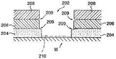
첨부한 도 8a 및 도 8b는 예컨대 실리콘 재(材)(Si)로 제조된 웨이퍼(W) 표면에 형성된 드레인이나 소스에 전기적 콘택트를 취하기 위한 콘택트 홀(202)을 도시하며, 도 8a에 도시된 홀 직경(D)은 0.2∼0.3㎛ 정도이다. 이 홀(202)의 다층 구 조의 벽면은 도 8a에 도시된 바와 같이, 다른 박막 형성 공정에서 형성된 예컨대 3층 구조의 실리콘 산화막(SiO2)으로 이루어진다. 여기서, 예컨대, 웨이퍼(W) 표면에 박막 형성된 제1층 SiO2막(204)은 열산화에 의해 형성된 막이며, 제2층 SiO2막(206)은 스핀 코팅(spin coating)법에 의해 형성된 인이 도포된 글라스이며, 또한 제3층 SiO2막(208)은 실리카글라스(silica glass)에 의해 형성된다. 또한, 도 8a에 도시한 바와 같이, 콘택트 홀(202)의 저부에는 자연 산화막(210)이 생성된다.8A and 8B show a
이러한 3층 구조의 박막 형성층에 있어서, 각 층을 구성하는 SiO2막(204, 206, 208)은 습식 세정시, 화학액에 대한 에칭 속도가 각각 다르다. 따라서, 종래의 습식 세정에 있어서, 습식 세정으로써 자연 산화막(210)을 제거한 후에는, 도 8b에 도시한 바와 같이, 전술한 에칭 속도의 차이로 인해 홀(202) 측벽에는 요철(209)이 생성되거나 혹은 화학액이 침입하기 쉬운 각 층간의 경계 부분이 과도하게 깍여진다는(절단 부분 참조) 문제점이 있다.In such a three-layer thin film forming layer, the SiO2 films 204, 206, and 208 constituting each layer have different etching rates with respect to chemical liquid during wet cleaning. Therefore, in the conventional wet cleaning, after removing the
그래서, 이러한 종래의 습식 세정이 갖는 문제점을 해결하기 위해서, 화학액 을 이용하는 습식 세정 대신 에칭 가스를 이용하여 자연 산화막을 제거하는 소위 건식(dry) 세정(에칭)법 등 다양한 대안의 방법들이 제안되고 있다(예컨대, 일본 특허 공개 공보 평성 제4-206526호, 일본 특허 공개 공보 평성 제6-196455호 참조).Therefore, in order to solve the problems of the conventional wet cleaning, various alternative methods such as a dry cleaning (etching) method of removing a natural oxide film using an etching gas instead of a wet cleaning using a chemical liquid are proposed. (See, for example, Japanese Patent Laid-Open Publication No. 4-206526 and Japanese Patent Laid-Open Publication No. 6-196455).
통상적으로 건식 세정에 의한 자연 산화막 제거법으로서 아르곤 가스와 H2 가스에 의한 스퍼터(sputter) 에칭법을 채용한다.Usually, sputter etching by argon gas and H2 gas is adopted as a natural oxide film removal method by dry cleaning.
또한, 예컨대, 상기 일본 특허 공개 공보 평성 제4-206526호에 도시된 반도체 웨이퍼의 스루 홀의 매립 방법에 있어서, 전처리실에서 기초 금속의 일부를 노출시키는 노출 기반의 전처리, 특히 그 금속막의 표면에 존재하는 산화막을 ClF3 가스를 공급ㆍ가열하여 라이트 에칭으로써 소위 자연 산화막 등을 제거한다. 그리고, 전처리된 웨이퍼를 공기에 노출시키지 않고, 반송 수단으로써 전처리실에서 박막 형성실로 반송하여 금속의 선택 CVD 처리를 행한다.Further, for example, in the method of filling the through-hole of the semiconductor wafer shown in Japanese Patent Laid-Open No. 4-206526, the exposure-based pretreatment exposing a part of the base metal in the pretreatment chamber, particularly on the surface of the metal film. The so-called natural oxide film and the like are removed by light etching by supplying and heating ClF3 gas. Then, the pretreated wafer is not exposed to air, and is transferred from the pretreatment chamber to the thin film formation chamber as a transfer means to perform selective CVD treatment of the metal.
또한, 상기 일본 특허 공개 공보 평성 제6-196455호에 나타나는 웨이퍼의 처리 방법에서는 웨이퍼를 ClF3 가스와 H2 가스의 혼합 가스 분위기에 넣고, 이 혼합 가스에 자외선을 조사하여, 웨이퍼를 가열하지 않고 웨이퍼 상에 생성된 자연 산화막을 제거한다.In the wafer processing method shown in Japanese Patent Laid-Open No. 6-196455, the wafer is placed in a mixed gas atmosphere of ClF3 gas and H2 gas, and the mixed gas is irradiated with ultraviolet rays to heat the wafer. The native oxide film formed on the wafer is removed.
그러나, 종래의 아르곤 가스와 수소 가스에 의한 스퍼터 에칭법에서는 웨이퍼의 콘택트를 손상시킬 우려가 있으므로 저에너지의 건식 세정이 요구된다.However, in the conventional sputter etching method using argon gas and hydrogen gas, there is a risk of damaging the contact of the wafer, so low energy dry cleaning is required.
또한, 공지의 ClF3가스를 사용한 웨이퍼 세정은 다음과 같은 문제점을 갖고 있다.In addition, wafer cleaning using a known ClF3 gas has the following problems.
즉, 세정에 이용된 ClF3 가스로부터 발생하는 염소에 의해서, 웨이퍼 상의 금속막 등이 부식되어 최종 제품으로서 반도체 소자의 수율, 신뢰성이 저하된다는 문제점이 있다. 즉, ClF3 가스는 염소 함유 가스이므로, ClF3 가스를 이용하여 웨이 퍼 표면의 세정을 행한 후에는, 예컨대, 그 표면에 존재하는 실리콘이나 금속 등의 원자와 결합한 염소 원자 형태로 웨이퍼 상에 염소가 잔류하고, 이 잔류 염소에 의해서 웨이퍼 상에 형성된 금속막 등(예컨대 반도체 소자의 배선으로서 기능함)이 부식되기 때문에, 반도체 소자의 전기적 특성 등이 열화하고, 최종 제품인 반도체 소자의 신뢰성, 수율이 저하된다.That is, there is a problem that the chlorine generated from the ClF3 gas used for cleaning corrodes the metal film or the like on the wafer, thereby lowering the yield and reliability of the semiconductor device as a final product. That is, since the ClF3 gas is a chlorine-containing gas, after cleaning the surface of the wafer using the ClF3 gas, for example, chlorine on the wafer in the form of chlorine atoms bonded to atoms such as silicon or metal present on the surface thereof, And the residual chlorine corrodes the metal film or the like formed on the wafer (e.g., serves as a wiring for the semiconductor element), so that the electrical characteristics and the like of the semiconductor element deteriorate, and the reliability and yield of the final product, the semiconductor element, Degrades.
또한, ClF3 가스에 의한 반응이 과도하게 진행되어 웨이퍼를 손상시키고, 최종 제품으로서 반도체 소자의 수율, 신뢰성이 저하된다는 문제점도 있다. 즉, ClF3가스를 이용하여 웨이퍼 표면을 세정한 후에는, 자연 산화물 뿐만 아니라 웨이퍼 상에 형성된 예컨대, SiO2 등의 절연막, Al 등의 금속막도 ClF3 가스와 함께 반응하여 에칭된다. 그리고, 예컨대, 반도체 소자의 층간 절연막으로서 기능하는 절연막이나 반도체 소자의 배선으로서 기능하는 금속막 등이 과도하게 에칭되면, 반도체 소자의 전기적 특성 등이 열화하고, 최종 제품인 반도체 소자의 신뢰성, 수율이 저하된다.In addition, there is a problem that the reaction by ClF3 gas proceeds excessively, damaging the wafer, and lowering the yield and reliability of the semiconductor device as a final product. That is, after cleaning the surface of the wafer using ClF3 gas, not only the natural oxide but also an insulating film such as SiO2 , a metal film such as Al, and the like formed on the wafer are reacted and etched with the ClF3 gas. For example, when an insulating film serving as an interlayer insulating film of a semiconductor element, a metal film serving as a wiring of a semiconductor element, or the like is excessively etched, the electrical characteristics of the semiconductor element deteriorate, and the reliability and yield of the semiconductor device as a final product decrease. do.
본 발명은 이러한 종래의 피처리물 표면 세정에서의 문제점에 감안하여 이루어진 것으로, 반도체 소자 등의 제조 공정에 이용될 경우에 제품의 신뢰성을 향상시킬 수 있는 표면 처리 방법 및 장치를 제공하는 것을 목적으로 한다.SUMMARY OF THE INVENTION The present invention has been made in view of such problems in surface treatment of a conventional target object, and an object thereof is to provide a surface treatment method and apparatus which can improve the reliability of a product when used in a manufacturing process such as a semiconductor device. do.
상기 목적을 달성하기 위해서, 청구범위 제1항에 따른 발명은, ClF3 가스를 이용하여 피처리물의 표면을 세정하는 공정과, 세정 공정 후에 피처리물의 표면에 잔류하는 상기 ClF3가스로부터 발생하는 염소를 상기 표면으로부터 제거하는 염소 제거 공정을 포함하는 것을 특징으로 한다.In order to achieve the above object, the invention according to Claim 1, characterized in that, by using a ClF3 gas generated from the ClF3 gas remaining in the process, and the processed surface of the water after the cleaning step of cleaning the target surface of the water And a chlorine removal process for removing chlorine from the surface.
청구범위 제2항에 따른 발명은, 염소 함유 가스를 이용하여 피처리물의 표면을 세정하는 공정과, 세정 공정 후에 피처리물의 표면에 잔류하는 염소 함유 가스로부터 발생하는 염소를 상기 표면으로부터 제거하는 염소 제거 공정을 포함하는 것을 특징으로 한다.The invention according to claim 2 is a process for cleaning a surface of an object by using a chlorine-containing gas, and chlorine that removes chlorine generated from the chlorine-containing gas remaining on the surface of the object after the cleaning step from the surface. It is characterized by including a removal process.
청구범위 제3항에 따른 발명은, 염소 제거 공정이 환원 가스를 이용하여 피처리물의 표면에서 염소를 제거하는 공정을 포함하는 것을 특징으로 한다.The invention according to claim 3 is characterized in that the chlorine removal step includes a step of removing chlorine from the surface of the workpiece using a reducing gas.
청구범위 제4항에 따른 발명은, 환원 가스가 H2 가스인 것을 특징으로 한다.The invention according to claim 4 is characterized in that the reducing gas is H2 gas.
청구범위 제5항에 따른 발명은, 피처리물의 표면에 ClF3 가스를 공급하여 피처리물의 표면에 ClF3 가스를 흡착시키는 흡착 공정과, 피처리물의 표면으로 ClF3 가스의 공급을 정지하는 공정과, 피처리물의 표면에 흡착된 ClF3 가스를 이용하여 피처리물의 표면을 세정하는 공정을 포함하는 것을 특징으로 한다.The invention according to claim 5 is an adsorption step of adsorbing ClF3 gas to the surface of the workpiece by supplying ClF3 gas to the surface of the workpiece, and a step of stopping the supply of ClF3 gas to the surface of the workpiece. And cleaning the surface of the object by using ClF3 gas adsorbed on the surface of the object.
청구범위 제6항에 따른 발명은, 피처리물의 표면에 세정 가스를 공급하여 피처리물의 표면에 세정 가스를 흡착시키는 흡착 공정과, 피처리물의 표면으로 세정 가스의 공급을 정지하는 공정과, 피처리물의 표면에 흡착된 세정 가스를 이용하여 피처리물의 표면을 세정하는 공정을 포함하는 것을 특징으로 한다.The invention according to claim 6 includes: an adsorption step of supplying a cleaning gas to the surface of the workpiece to adsorb the cleaning gas to the surface of the workpiece, a step of stopping supply of the cleaning gas to the surface of the workpiece, and And cleaning the surface of the object by using a cleaning gas adsorbed on the surface of the object.
청구범위 제7항에 따른 발명은, 흡착 공정에서 피처리물을 20℃ 이하로 냉각하는 것을 특징으로 한다.The invention according to claim 7 is characterized in that the object to be treated is cooled to 20 ° C. or lower in the adsorption step.
청구범위 제8항에 따른 발명은, 내부에 피처리물이 배치되는 처리 용기와, 처리 용기 내에 ClF3 가스를 공급하는 수단과, 공급된 ClF3 가스를 활성화하는 수단과, 처리 용기 내에 환원 가스를 공급하는 수단을 구비하는 것을 특징으로 한다.The invention according to Claim 8, characterized in that, to the processing target object is placed in the interior of the vessel, it means for supplying ClF3 gas into the processing vessel, and means for activating the supply ClF3 gas and a reducing gas into the treatment vessel It characterized in that it comprises a means for supplying.
청구범위 제9항에 따른 발명에 있어서, 내부에 피처리물이 배치되는 처리 용기와, 처리 용기 내에 ClF3 가스를 공급하는 수단과, 피처리물에 ClF3 가스의 흡착을 촉진하는 수단과, 공급된 ClF3가스를 활성화하는 수단을 구비하는 것을 특징으로 한다.In the invention according to claim 9, there is provided a treatment vessel in which a workpiece is disposed, a means for supplying ClF3 gas into the treatment vessel, a means for promoting adsorption of ClF3 gas on the workpiece, And means for activating the supplied ClF3 gas.
청구범위 제10항에 따른 발명에 있어서, 처리 용기 내에 설치되고, 피처리물을 적재하는 적재대를 구비하는 것을 특징으로 한다.In the invention according to
청구범위 제11항에 따른 발명에 있어서, 피처리물에 ClF3 가스의 흡착을 촉진하는 수단은 적재대 내에 설치되고, 상기 적재대 상에 적재된 피처리물을 냉각하는 수단인 것을 특징으로 한다.In the invention according to
청구범위 제12항에 따른 발명은, ClF3 가스를 활성화하는 수단은 적재대의 피처리물 적재부로부터 이격된 가열 위치에서 피처리물을 가열하는 수단인 것을 특징으로 한다.The invention according to
청구범위 제13항에 따른 발명은, 피처리물 적재부와 가열 위치 사이에서 피처리물을 승강시키는 수단을 구비하는 것을 특징으로 한다.
청구범위 제14항에 따른 발명은, 청구범위 제8항 내지 제13항 중 어느 한 항에 기재된 표면 처리 장치와, 내부를 비반응성 분위기로 유지시킬 수 있음과 동시에 표면 처리 장치 사이에서 피처리물을 비반응성 분위기 속에서 반송가능하도록 설치된 반송실와, 반송실 사이에서 피처리물을 비반응성 분위기 속에서 반송가능하도록 설치된 1 이상의 다른 처리 장치를 구비하는 것을 특징으로 한다.
청구범위 제15항에 따른 발명은, 상기 다른 처리 장치가 피처리물 상에 금속 배선을 형성하기 위한 금속 배선 형성실인 것을 특징으로 한다.The invention according to
The invention according to
The invention according to
도 1은 본 발명의 표면 처리 장치의 일실시예의 모식 구성도이다.1 is a schematic configuration diagram of an embodiment of a surface treatment apparatus of the present invention.
도 2a 및 도 2b는 도 1에 도시한 표면 처리 장치에 이용되는 웨이퍼 리프트(lifting) 기구를 도시하고, 도 2a는 그 평면도이고, 도 2b는 그 측면도를 도시하는 도면이다.2A and 2B show a wafer lifting mechanism used in the surface treatment apparatus shown in FIG. 1, FIG. 2A is a plan view thereof, and FIG. 2B is a view showing a side view thereof.
도 3a 및 도 3b는 도 1에 도시한 표면 처리 장치에 이용하는 ClF3 가스 공급부(샤워 헤드)의 변형예를 도시하고, 도 3a는 웨이퍼 적재대측으로부터 링형의 샤워 헤드를 본 상태를 도시하는 평면도이고, 도 3b는 격자형의 샤워 헤드를 본 상태를 도시하는 평면도이다.3A and 3B show a modification of the ClF3 gas supply unit (shower head) used in the surface treatment apparatus shown in FIG. 1, and FIG. 3A is a plan view showing a state of seeing a ring-shaped shower head from the wafer mounting table side. 3B is a plan view showing a state of a grid-shaped shower head.
도 4는 본 발명의 표면 처리 방법의 일실시예의 각 공정을 도시하는 플로우 차트이다.Fig. 4 is a flowchart showing each step of the embodiment of the surface treatment method of the present invention.
도 5a, 도 5b 및 도 5c는 본 발명의 표면 처리 방법의 일실시예의 공정을 도시한 도면으로서, 도 5a는 웨이퍼에 부착된 자연 산화물의 부착 상태의 확대도이고, 도 5b는 웨이퍼 상에서 ClF3 가스의 흡착 상태의 확대도이며, 도 5c는 플라즈마에 의해 활성화된 환원 가스(H2 가스)로써 잔류 염소를 제거하는 상태를 나타내는 확대 모식도이다.5A, 5B and 5C show a process of one embodiment of the surface treatment method of the present invention, FIG. 5A is an enlarged view of the adhesion state of the native oxide attached to the wafer, and FIG. 5B is ClF3 on the wafer. the expansion of the adsorbed state of the gas, and Fig. 5c is a schematic enlarged view showing a state of removing the residual chlorine as a reducing gas (H2 gas) activated by a plasma.
도 6a 및 도 6b는 웨이퍼 적재대의 다른 예를 도시하는 도면으로서, 도 6a는 그 평면도이고, 도 6b는 그 정단면를 나타내는 도면이다.6A and 6B are views showing another example of the wafer mounting table, in which FIG. 6A is a plan view thereof, and FIG. 6B is a view showing a front end surface thereof.
도 7은 도 1에 도시한 본 발명의 일실시예인 표면 처리 장치를 진공 세정 장치로서 이용하여 가열 장치, 배선 형성 장치 및 냉각 장치와 조합하여 구성한 진공 클러스터 장치의 개념도이다.FIG. 7 is a conceptual diagram of a vacuum cluster apparatus constructed by combining a heating apparatus, a wiring forming apparatus, and a cooling apparatus by using the surface treatment apparatus shown in FIG. 1 as a vacuum cleaning apparatus.
도 8a 및 도 8b는 자연 산화막을 제거하는 종래의 표면 처리 방법을 설명하 는 도면으로서, 도 8a는 웨이퍼의 콘택트 홀의 저부에 생성된 자연 산화막의 부착상태를 도시하는 확대도이며, 도 8b는 콘택트 홀의 측벽에 요철 등이 형성된 상태를 도시하는 확대 모식도.8A and 8B illustrate a conventional surface treatment method of removing a native oxide film, wherein FIG. 8A is an enlarged view showing a state of adhesion of a native oxide film formed at the bottom of a contact hole of a wafer, and FIG. 8B is a contact. An enlarged schematic diagram showing a state in which unevenness is formed on the sidewall of the hole.
이하, 첨부 도면을 참조하여, 본 발명의 표면 처리 방법과 이 방법을 이용하는 표면 처리 장치의 일실시예를 설명한다.EMBODIMENT OF THE INVENTION Hereinafter, with reference to an accompanying drawing, one Embodiment of the surface treatment method of this invention and the surface treatment apparatus using this method is demonstrated.
표면 처리 장치의 구성Composition of Surface Treatment Unit
도 1은 본 발명의 표면 처리 장치의 실시예의 일례를 도시하는 개념 구성도이다. 도 1에 도시된 표면 처리 장치(세정 장치: 1)는 반도체 소자 등의 제조 공정에 있어서, 예컨대, 콘택트 홀(202)(도 8a 참조) 등이 형성된 웨이퍼(W)(피처리물)의 표면 세정에 이용된다. 이 세정에 의해서, 콘택트 홀(202) 등의 저부 표면에 생성된 자연 산화막 혹은 화학 산화물로서, 그 막 두께가 10∼20 Å정도인 산화물(이하, 「자연 산화물」이라고 함) 혹은 콘택트 홀(202) 등의 저부나 측벽부 표면에 부착된, 예컨대 금속 등의 오염물이 제거된다.BRIEF DESCRIPTION OF THE DRAWINGS It is a conceptual block diagram which shows an example of the Example of the surface treatment apparatus of this invention. The surface treatment apparatus (cleaning apparatus 1) shown in FIG. 1 is the surface of the wafer W (process object) in which the contact hole 202 (refer FIG. 8A) etc. was formed in manufacturing processes, such as a semiconductor element. Used for cleaning. As a result of this cleaning, a natural oxide film or a chemical oxide formed on the bottom surface of the
그리고, 표면 처리 장치(1)는 H2 가스 등의 환원 가스를 플라즈마화하여 활성화하는 플라즈마 형성관(30)과, 피처리물인 웨이퍼(W)를 수용하여 그 표면을 세정하기 위해서 소정의 표면 처리를 하는 처리(반응) 용기(10)와, 이 처리 용기(10) 내에 세정 가스로서 ClF3혼합 가스를 공급하는 세정 가스 공급관(26)으로 주로 구성되어 있다.Then, the surface treatment apparatus 1 receives a
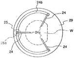
처리 용기(10)는 알루미늄 재료로 제조되고, 그 내벽은 석영(SiO2) 라이닝(linings)(13, 14)으로 코팅되어 웨이퍼(W)의 금속 오염, 처리 용기(10)의 알루미늄 표면의 침식 등이 억제된다. 이 처리 용기(10)는 통형의 하우징체로서, 그 횡단면은 원형, 사각형, 다각형의 어느 것이라도 양호하다.The
이 처리 용기(10)의 저부에는 소정 두께의 하판(12)이 끼워 붙여져 있고, 이 하판(12) 상에는 그 표면을 석영으로 덮은 베이스(29)가 배치되며, 이 베이스(29)에는 석영에 의해서 웨이퍼 적재부 이외를 덮은 원통형의 웨이퍼 적재대(서셉터: 20)가 세워져 설치되어 있다. 이 웨이퍼 적재대(20)의 거의 수평인 상면에는 피처리물인 웨이퍼(W)가 석영으로 제조된 클램프 링(21)에 의해 걸어 멈춰지도록 되어 있다. 또한, 원통형의 적재대(20)의 내부에는 냉각 매체(칠러(chiller))를 수납하는 재킷(혹은 파이프: 22)을 갖는 열 교환체(23)가 충전되고, 냉각 매체 공급 장치(42)에서 냉각관로(43)를 통해 웨이퍼(W)를 소정의 온도, 예컨대 20℃ 이하의 온도로 냉각하기 위해서 냉각 매체가 재킷(혹은 파이프: 22) 내에 공급되어 이 냉각계를 순환하도록 되어 있다.A
또한, 적재대(20)에는 후술하는 바와 같이, 적재된 웨이퍼(W)를 가열할 때에 적재대(20)의 웨이퍼 적재부로부터 이격된 가열 위치까지 상승시키는 핀 구동 장치(25)에 의해 승강되는 웨이퍼 리프트 수단(24)이 배치되어 있다. 이 웨이퍼 리프트 수단(24)은 도 2a 및 도 2b에 각각 도시한 바와 같이 구성되어 있고, 처리 용기(10)의 하부에 배치된 적재대(20)의 베이스(29)의 하면에 액압 실린더(25: 핀 구 동 장치)가 배치되며, 그 실린더 로드(25a)의 선단부에는 말굽 형상의 지지 부재(24b)가 고착되어 있다. 그리고, 이 지지 부재(24b)에서 반경 방향 안쪽으로 연장된 아암(24)의 소정 부분, 예컨대 세 부분에 위쪽으로 돌출한 그 선단부에 뾰족한 두부(頭部)를 갖는 지지핀(24a)을 세워 설치하고, 지지핀(24a)으로부터 웨이퍼(W)를 3점 지지하여 거의 수평으로 유지한다. 그리고, 가열 램프(19)에 의한 웨이퍼 가열시, 액압 실린더(25)를 작동시켜 웨이퍼(W)를 전술한 가열 위치까지 상승시키도록 되어 있다.In addition, as described later, the mounting table 20 is lifted by a
또한, 도 1에 도시한 바와 같이, 처리 용기(10)의 저부에 끼워 붙인 하판(12)의 주연부에는, 예컨대 4개의 배기관(40)이 설치되어 있고, 이 배기관(40)에 각각 접속된 진공 펌프(기압 양수기) 등의 배기 수단(41)에 의해 처리 용기(10) 내부를 탈기할 수 있다.In addition, as shown in FIG. 1, four
한편, 처리 용기(10)의 상부에는 알루미늄재로 제조된 상판(11)이 고착되고, O-링 등의 밀봉 부재(17)를 통해 플랜지부(16)를 갖는 석영으로 제조된 돔(덮개: 15)이 배치된다. 이 돔(15)은 석영으로 제조된 플라즈마 형성관(30)과 일체로 형성되어 있기 때문에, 이들을 지지하기 위한 기계적 강도가 충분하게 취해지는 것이면 양호하고, 그 형상은 돔 형상 뿐만 아니라, 평탄한 석영판도 양호하다.On the other hand, a
또한, 밀봉 부재(17)가 배치된 밀봉부에는 압력 센서 등이 배치되어 밀봉부의 체결 압력이나 밀봉부로부터 가스 누설을 방지하도록 감시할 수 있다.Moreover, a pressure sensor etc. are arrange | positioned at the sealing part in which the sealing
또한, 돔(15)의 위쪽에는, 웨이퍼(W)를 그 위쪽으로부터 가열하여 웨이퍼(W) 상의 ClF3가스를 활성화하기 위한 다수의 가열 램프(19)가 배치되어 있다. 이 가열 램프(19)는 급속 승온을 가능하도록 할로겐 램프 등으로 이루어지고, 이 가열 램프(19)로부터 방출되는 열선이 투명한 석영으로 제조된 돔(15)을 투과하여 전술한 가열 위치까지 상승된 웨이퍼(W)의 표면에 입사하여 웨이퍼(W)를 소정의 온도, 예컨대 150℃ 이하의 온도로 가열하도록 되어 있다.Further, above the
또한, 가열 램프(19)군은 금속 등으로 이루어지는 커버(18)에 의해 덮어지므로 가열 램프(19)로부터 외부로 열선 및 광선을 차단함과 동시에, 석영으로 제조된 돔(15)이 파손될 지라도 ClF3나 H2 등의 세정 가스 및 환원 가스가 외부로 확산 및 일출(溢出)되는 것을 막을 수 있다.In addition, since the
또한, ClF3가스를 활성화하기 위한 수단으로서, 자외선을 조사하기 위한 광원을 이용해도 좋다.As a means for activating the ClF3 gas, a light source for irradiating ultraviolet rays may be used.
또한, 처리 용기(10)의 측벽에는 웨이퍼(W)의 반출 반입시에 개폐되는 게이트 밸브(10a)가 설치되어 접속되는 반송실과 그 개방시에 연통하도록 되어 있다. 게이트 밸브(10a) 내면도 석영으로 코팅되어 보호된다.In addition, the side wall of the
또한, 환원 가스를 도입하여 플라즈마화하기 위한 석영으로 제조된 플라즈마 형성관(30)이 동일하게 석영으로 제조된 돔(15)의 상부 중앙에 용융 접합 등으로써 일체로 연결되어 돔(15)의 중앙에서 처리 용기(10)에 개구하고 있다.In addition, the
이 플라즈마 형성관(30)의 상단부에는, 이 속에 환원 가스인 H2가스를 도입 하는 환원 가스 도입부(33)가 접속되어 있고, H2가스원(36)으로부터 유량 제어기(MFC: 34)를 통해 가스 통로(33A)에 H2가스를 공급하여 환원 가스로서 유도 코일(35)이 권취된 플라즈마 형성관(30)의 플라즈마 발생부로 공급하도록 되어 있다.To the upper end of the
이 유도 코일(35)에는, 예컨대 13.56 MHz의 고주파(RF(Radio Frequency)파)를 발생하는 고주파 전원(32)이 임피던스 매칭을 행하는 정합 회로(31)를 통해 접속되어 있다. 고주파 전력을 유도 코일(35)에 공급함으로써 플라즈마 발생부에 공급되는 환원 가스는 플라즈마화되고, 활성 가스종으로서 플라즈마 형성관(30)의 개구부(30a)로부터 처리 용기(10) 내에 공급된다.The
또한, 플라즈마 발생원으로서 마이크로파 방전관을 이용해도 양호하다.Moreover, you may use a microwave discharge tube as a plasma generation source.
또한, 플라즈마 형성관(30)의 개구부(30a)의 아래쪽에 처리 용기 내에 세정 가스로서 ClF3가스를 공급하는 다수의 가스 분출 구멍(26a)이(바람직하게는 거의 수평인 면, 즉 적재대(20) 상에 적재된 웨이퍼(W)의 표면에 거의 평행한 면을 따라서 거의 같은 간격으로 배치되어) 설치되어 있다. 이들 가스 분출 구멍(ClF3 가스 공급부: 26a)은 도통관(26)에 처리 용기(10)의 외벽에 두루 설치된 링형의 배관(26b)을 통해 접속되고, 이 도통관(26)은 유량 제어기(MFC: 27)를 통해 ClF3 가스원(28)에 접속되어 소정 유량의 ClF3 가스를 다수의 가스 분출 구멍(26a)으로부터 처리 용기(10) 내에 공급할 수 있다.Further, a plurality of gas ejection holes 26a for supplying ClF3 gas as a cleaning gas in the processing vessel below the
본 명세서에서는, 도 1에서 이 가스 분출 구멍(26a)이 처리 용기(10)의 내벽면으로부터 약간 안쪽에 돌출한 파이프형인 것의 선단부에 개구된 것으로 했지만, 처리 용기(10)의 내벽면에 가스 분출 구멍(26a)을 직접 개구시켜도 양호하다.In this specification, although the
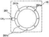
또한, 도 3a에 도시한 바와 같이, 석영으로 제조된 링형의 샤워 헤드(261b)를 구성하고, 이 샤워 헤드(261b)에 다수의 가스 분출 구멍(216a)을 그 원주 상에 (바람직하게는 그 원주 상에 거의 같은 간격으로 배치하여) 아래쪽(적재대(20)의 방향)을 향하여 개구하며, 도통관(261)을 이 링형의 샤워 헤드(261a)에 접속한 것을 처리 용기(10) 내의 소정 위치에(바람직하게는 거의 수평으로) 배치하여 ClF3 가스를 처리 용기(10) 내에 공급하여도 양호하다.In addition, as shown in Fig. 3A, a ring-shaped
또한, 도 3b에 도시한 바와 같이 샤워 헤드(262b)를 격자형으로 형성하여 다수의 가스 분출 구멍(262s)을 소정의 부분에(바람직하게는 그 격자 상에 거의 같은 간격으로 배치하여) 개구시키고, 이 격자형의 샤워 헤드(262b)에 도통관(262)을 접속한 것을 처리 용기(10) 내의 소정 위치에(바람직하게는 거의 수평으로) 배치하여 ClF3가스를 처리 용기(10) 내에 공급하여도 양호하다.In addition, as shown in FIG. 3B, the
전술한 바와 같이, ClF3 가스 공급 수단을 다수의 가스 분출구를 갖도록 구성함으로써, ClF3가스를 다수의 가스 분출 구멍으로부터 샤워형으로 처리 용기(10) 내에 공급하고, 적재대(20) 상에 적재된 웨이퍼(W) 상에 남김없이 균등하게 흘러 내려보낼 수 있다.As described above, by configuring the ClF3 gas supply means to have a plurality of gas ejection openings, the ClF3 gas is supplied into the
표면 처리 방법의 구성Composition of Surface Treatment Methods
다음에, 본 발명의 표면 처리 방법의 실시예의 1예인, 이상과 같이 구성된 표면 처리(세정) 장치(1)를 이용한 표면 처리(세정) 방법에 관해서 도 4(플로우 차트)에 기초하여 설명한다.Next, the surface treatment (cleaning) method using the surface treatment (cleaning) apparatus 1 comprised as mentioned above which is an example of the Example of the surface treatment method of this invention is demonstrated based on FIG. 4 (flow chart).
도 1에 도시하는 표면 처리 장치(1)에 있어서, 우선, 진공 펌프(기압 양수기: 41)를 작동시키고 배기관(40)을 통해 탈기함으로써, 처리 용기(10) 내부는 진공(예컨대 1∼3 Torr)이 되게 한다.In the surface treatment apparatus 1 shown in FIG. 1, first, by operating a vacuum pump (atmospheric water pump 41) and degassing through the
다음에, 피처리물인 웨이퍼(W) 1장을 게이트 밸브(10a)를 개방하여 인접하는, 예컨대 진공 반송실로부터 처리 용기(10) 내에 반입한다. 웨이퍼(W)를 적재대(서셉터: 20) 상에 적재한 후, 게이트 밸브(10a)를 폐쇄하고 클램프 링(21)을 작동시켜 웨이퍼(W)를 적재대(20)에 걸어 멈춘다(단계 S301). 이때, 이 웨이퍼(W)에는, 예컨대 전공정에 있어서 콘택트 홀(202)(도 7 참조)이 형성되어 있고, 이 홀 저부 표면에는 도 5a에 도시한 바와 같은 막 두께 10∼20 Å의 자연 산화물(80)이 생성된다.Next, one wafer W, which is an object to be processed, is loaded into the
그 후, ClF3(3불화 염소) 가스를 유량 제어기(MFC: 27)로 소정의 유량으로 제어하면서 세정 가스 공급관(26)에 공급한다. 그리고, ClF3가스를 처리 용기(10) 내에 개구한 다수의 가스 분출 구멍(26a)으로부터 샤워형으로 공급하고, 적재대(20) 상에 적재된 웨이퍼(W) 상에 남김없이 균등하게 흘러 내려보낸다(단계 S302).Thereafter, ClF3 (chlorine trifluoride) gas is supplied to the cleaning
이 때, 도 1에 도시하는 냉각 매체 공급 장치(42)를 작동시키고, 냉각 매체( 예컨대, 에틸렌 글리콜)를 적재대(20) 내에 공급하여 적재대(20)를 냉각하며, 적재대(20) 상의 웨이퍼를 냉각한다. 적재대(20) 상의 웨이퍼(W)가 냉각되며, 이 냉각에 의해, 웨이퍼(W)로 ClF3 가스 흡착이 촉진되고, 웨이퍼(W) 상에 ClF3 가스가 잘 흡착된다(단계 S303). 발명자의 실험에 의하면, 웨이퍼(W)의 표면 온도가 10O℃ 이하의 온도 영역에서는 ClF3은 거의 분해되지 않고, 약간량이 웨이퍼(W)의 표면에 흡착될 뿐이다. 이에 대하여, 웨이퍼(W)의 표면 온도가 낮은 경우에는 ClF3의 흡착량이 증가한다. 따라서, ClF3 가스를 웨이퍼(W)의 표면에 효율적으로 흡착시키기 위해, 웨이퍼(W)의 표면 온도를 20℃ 이하의 온도로 냉각한다. 이렇게 하여, 도 5b에 도시한 바와 같이, 웨이퍼(W) 상에 ClF3 가스(81)를 흡착시킨다.At this time, the cooling
계속해서, 처리 용기(10) 내에 ClF3가스 도입을 정지한다(단계 S304). 이 때, 처리 용기(10) 내는 진공 배기되어 있다.Subsequently, the introduction of ClF3 gas into the
또한, 실온에서는 ClF3이 거의 반응하지 않으므로(자연 산화물(80) 등이 제거되지 않고, 웨이퍼(W)의 표면이 세정되지 않음), 이 상태에서 클램프 링(21)을 작동시켜 적재대(20)에서 웨이퍼(W)의 걸어 멈춤을 해제하고, 웨이퍼 리프트 수단(24)을 구동시켜 웨이퍼(W)를 전술한 가열 위치까지 상승시킨다(단계 S305). 그리고, 가열 수단의 가열 램프(19)를 점등시키고, 가열 램프(19)에 의해 웨이퍼(W)의 위쪽에서부터 그 표면을 가열한다. 이렇게 하여, 웨이퍼(W)의 온도를 실온으로부터 급속히 소정의 온도, 예컨대 150℃의 온도까지 상승시킨다(단계 S306).In addition, since ClF3 hardly reacts at room temperature (the
이 가열 램프(19)를 이용하여 150℃ 온도로의 급속 가열함으로써, 웨이퍼(W) 상에 흡착된 ClF3가스는 표면 상에서 열분해되어 활성화된다. 그리고, 웨이퍼(W) 표면의 자연 산화물(80) 등이 제거되고, 웨이퍼(W) 표면이 세정된다(단계 S307). 세정 후, 가열 램프(19)를 소등한다(단계 S308).By rapid heating to a temperature of 150 ° C using this
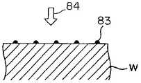
이렇게 ClF3가스를 이용하여 웨이퍼(W) 표면을 세정한 후에는, 도 5c에 도시한 바와 같이, 웨이퍼(W) 표면 세정에 이용한 ClF3 가스로부터 발생하는 염소(83)가 예컨대, 웨이퍼(W)의 표면을 구성하는 원자에 결합한 염소 원자 형태로 잔류한다.After cleaning the surface of the wafer W using ClF3 gas in this manner, as shown in FIG. 5C,
따라서, 도 1에 도시된 H2 가스원(36)으로부터 유량 제어기(34)를 통해 가스 통로(33A)에 환원 가스로서 H2 가스를 공급한다. 유도 코일(35)에 고주파 전력을 공급함으로써, 가스 통로(33A)에 공급된 H2가스는 플라즈마 형성관(30) 내에서 플라즈마화되고, 활성 가스종으로서 플라즈마 형성관(30)의 개구부(30a)로부터 처리 용기(10) 내에 적재된 웨이퍼(W) 상에 흘러 내려간다(단계 S309). 그리고, 도 5c에 도시한 바와 같이, 상기 H2 환원 가스(84)는 웨이퍼(W) 상에 잔류하는 염소(83)를 환원 작용에 의해 웨이퍼(W) 표면으로부터 제거한다(단계 S310).Therefore, the H2 gas is supplied as the reducing gas to the gas passage 33A from the H2 gas source 36 shown in FIG. 1 through the
또한, 이 환원 가스에 의한 잔류 염소의 제거를 처리 용기(10) 이외 별도의 실(chamber)에서 수행하여도 양호하다. 또한, 환원 가스를 플라즈마화하지 않은채 처리 용기(10) 내에 도입하여, 가열 램프(19)에 의해서 웨이퍼(W)를 소정의 온도에 가열함으로써, 웨이퍼(W)로부터 잔류 염소를 제거해도 양호하다.In addition, removal of residual chlorine by this reducing gas may be performed in a chamber other than the
그 후, 환원 가스 도입을 정지한다(단계 S311). 이때, 처리 용기(10) 내는 진공 배기되어 있다.Thereafter, introduction of the reducing gas is stopped (step S311). At this time, the inside of the
마지막으로, 도 1에 도시하는 게이트 밸브(10a)를 개방하여 표면 세정이 종료된 웨이퍼(W)를 처리 용기(10) 내로부터 반출하고, 예컨대, 인접하는 진공 반송실에 복귀시킨다(단계 S312). 그 후, 게이트 밸브(10a)를 폐쇄한 후에, 다음 공정, 예컨대, 진공 반송실과 인접한 가열실로 웨이퍼(W)를 반송 로봇 등에 의해 반입한다.Finally, the
전술의 표면 처리 방법에서는, 웨이퍼(W)의 표면에 ClF3가스를 공급하여 웨이퍼(W)의 표면에 ClF3 가스를 흡착시키고, 웨이퍼(W)의 표면으로 ClF3 가스 공급을 정지한 후에 웨이퍼(W)의 표면에 흡착한 ClF3 가스를 이용하여 웨이퍼(W)의 표면을 세정하도록 했다. 그 때문에, 반응하는 ClF3의 양을 웨이퍼의 표면에 흡착된 양 또는 그 이하로 제한하여 ClF3 가스에 의한 반응의 진행 정도를 제어할 수 있고, 웨이퍼(W) 상에 형성되어 있는 절연막이나 금속 배선막 등이 과도하게 에칭되는 것을 억제할 수 있다.In the method for surface treatment of the foregoing description, after adsorbed the ClF3 gas to the surface of the wafer (W) the wafer (W) by supplying ClF3 gas to the surface of, stops the ClF3 gas supply to the surface of the wafer (W) wafer The surface of the wafer W was cleaned using ClF3 gas adsorbed onto the surface of (W). Therefore, the amount of reacted ClF3 is limited to the amount adsorbed on or below the surface of the wafer to control the progress of the reaction by the ClF3 gas, and the insulating film or metal formed on the wafer W can be controlled. Excessive etching of the wiring film or the like can be suppressed.
또한, 웨이퍼(W)의 표면 온도를 20℃ 이하의 온도로 냉각하여 웨이퍼(W)에 ClF3 가스 흡착을 촉진하고 있기 때문에, ClF3가스를 웨이퍼(W)의 표면에 효율적으로 흡착시킬 수 있다.Also, since the promotion of ClF3 gas adsorbed on the wafer (W) is cooled to a temperature below 20 ℃ the surface temperature of the wafer (W), can be efficiently adsorbed to the ClF3 gas to the surface of the wafer (W) .
또한, 웨이퍼(W) 가열시, 적재대(20)의 웨이퍼 적재부로부터 이격된 가열 위치까지 웨이퍼(W)를 상승시키기 때문에, 적재대(20)와 웨이퍼(W) 사이의 열전달이 억제되어 웨이퍼(W)를 효율적으로 가열할 수 있다.In addition, during the heating of the wafer W, the wafer W is raised to a heating position spaced apart from the wafer loading portion of the mounting table 20, so that heat transfer between the mounting table 20 and the wafer W is suppressed and the wafer (W) can be heated efficiently.
또한, ClF3가스를 이용하여 웨이퍼(W)의 표면을 세정하고, 환원 가스를 이용하여 웨이퍼(W)의 표면에 잔류하는 상기 ClF3 가스로부터 발생하는 염소를 제거할 수 있기 때문에, 상기 염소에 의해서 웨이퍼(W) 상의 금속막 등이 부식되는 것을 억제할 수 있다.In addition, since the chlorine generated from the ClF3 gas remaining on the surface of the wafer W can be removed by using a ClF3 gas, the surface of the wafer W can be cleaned. As a result, the corrosion of the metal film or the like on the wafer W can be suppressed.
또한, 환원 가스로서 H2 가스를 이용하기 때문에, 웨이퍼 상의 잔류 염소와 환원 가스의 반응 생성물은 휘발성 염화 수소가 되고, 상기 반응 생성물을 용이하게 처리 용기 밖으로 배출할 수 있다.In addition, since H2 gas is used as the reducing gas, the reaction product of the residual chlorine and the reducing gas on the wafer becomes volatile hydrogen chloride, and the reaction product can be easily discharged out of the processing vessel.
또한, 전술의 표면 처리 방법은 Si 상에 생성된 자연 산화물을 제거하는 경우 이외에도, 예컨대, W, Ti, A1, Ni, Co 및 이들의 실리사이드 상에 성장한 극히 얇은(10∼20 Å정도) 산화물 제거할 경우에도 적용할 수 있다.In addition, the surface treatment method described above removes extremely thin (about 10 to 20 kPa) oxides grown on, for example, W, Ti, A1, Ni, Co, and silicides thereof, in addition to removing natural oxides formed on Si. This can also be applied.
또한, 전술한 표면 처리 방법은 콘택트 홀이 형성된 웨이퍼(W) 표면을 세정하는 경우 이외에도 예컨대, 비어홀이 형성된 웨이퍼(W) 표면을 세정할 경우에도 적용할 수 있다.In addition, the above-described surface treatment method can be applied not only to cleaning the surface of the wafer W on which the contact holes are formed, but also to clean the surface of the wafer W on which the via holes are formed.
웨이퍼wafer 지지 수단의 다른 Other of support means실시예Example
다음에, 웨이퍼 지지 수단의 다른 실시예에 관해서 도 6a 및 도 6b를 참조하여 설명한다.Next, another embodiment of the wafer support means will be described with reference to Figs. 6A and 6B.
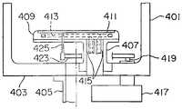
이 도면에 있어서, 부호 401은 처리 용기를 나타낸다. 이 처리 용기(401)의 저부에는 하판(403)이 설치되어 있고, 이 하판(403)의 중심부에는 배기관(405)이 설치된다.In this figure,
한편, 하판(403) 중, 배기관(405)이 설치된 중심부로부터 편심한 위치에는 통형의 적재대 지지부(407)가 세워져 설치되어 있다. 이 적재대 지지부(407)에는 원반형의 웨이퍼 적재대(409)가 고정되어 있다. 이 웨이퍼 적재대(409)는 그 상면에 웨이퍼를 적재한 오목부(411)가 형성되고, 이 오목부(411)에 웨이퍼가 적재되도록 되어 있다.On the other hand, in the
또한, 웨이퍼 적재대(409)의 내부에는 이 적재대를 냉각하기 위한 냉매를 순환시키는 냉매 통로(413)가 형성되어 있다. 이 냉매 통로(413)는 웨이퍼 적재대(409)를 균일하게 냉각할 수 있도록 웨이퍼 적재대의 외주부 및 중심부의 전역에 걸쳐 배치되어 있다. 이 냉매 통로(413)에는 한 쌍의 냉매 관로(415)가 접속되어 있다. 이 한 쌍의 냉매 관로(415)는 통형의 적재대 지지부(407)의 내부를 통하여 배관되고, 냉매 공급 수단(도시하지 않음)에 접속되어 있다. 그리고, 웨이퍼 적재대(409)에 냉매를 공급 및 배출함으로써, 웨이퍼를 냉각할 수 있게 되고 있다.In addition, a
한편, 상기 하판(403) 중, 배기관(405)이 설치된 중심부로부터 편심한 위치에서, 상기 적재대 지지부(407)로부터 주위 방향에 소정 각도로 이격된 위치에는 핀 구동 장치(417)가 고정되어 있다. 이 핀 구동 장치(417)는 그 내부에 모터 등의 구동원을 가지고 있고, 이 구동원에 의해서 구동되는 로드(419)가 처리 용기(401) 내부에 돌출된다. 이 로드(419)의 상단에는 메인 아암(421)이 고정되어 있고, 이 메인 아암(421)은 이 처리 용기(401)의 중심부를 향하여 돌출하여 설치되어 있다. 이 메인 아암(421)의 선단에는 3가지의 서브 아암(423)이 설치되어 있다. 이 3가지의 서브 아암(423)은 인접하는 서브 아암끼리 각각 120。를 이루도록 반경 방향 바깥쪽으로 돌출하여 형성되어 있다. 각각의 서브 아암(423)의 선단에는 위쪽으로 돌출형성된 리프트 핀(425)이 설치되어 있다. 이 리프트 핀(425)은 웨이퍼 적재대에 형성된 구멍부에 삽입된 상태로 배치되어 있다. 이러한 구성에 있어서, 우선 핀 구동 장치(417) 내의 구동원을 구동함으로써, 로드(419)를 상하 이동시킨다. 그리고, 메인 아암(421) 및 서브 아암(423)을 통해 리프트 핀(425)을 승강시킴에 따라 웨이퍼 적재대(409) 상의 웨이퍼를 승강시킬 수 있다.On the other hand, in the
이 웨이퍼 지지 수단에 있어서, 적재대 지지부(407), 핀 구동 장치(417)를 처리 용기(401)의 외주부에 배치함으로써, 배기관(405)을 하판(403)의 중앙부에 설치하므로, 처리 용기로부터 배기되는 기체의 유선을 처리 용기의 축선에 대하여 축 대상으로 형성할 수 있다. 따라서, 처리 용기 내부에서 분위기의 불균일을 방지할 수 있고 웨이퍼의 균일한 처리를 행할 수 있다.In the wafer support means, the
클러스터cluster(cluster) 장치의 구성(cluster) Device Configuration
이하에, 본 발명의 표면 처리 장치를 반송실을 통해 다른 처리 장치(예컨대 금속 배선 형성실)와 접속하여 구성한 멀티-실(室) 방식의 클러스터 장치의 일실시예에 관해서 설명한다.Hereinafter, an embodiment of the multi-room type cluster apparatus which connected the surface treatment apparatus of this invention with another processing apparatus (for example, metal wiring formation chamber) via the conveyance chamber is demonstrated.
도 7에 도시하는 클러스터 장치(100)는 본 발명의 처리 장치의 일실시예이고, 도 1에 도시하는 표면 처리 장치(1)를 진공 세정실(101)로서 진공 세정실(101), 가열실(102), 1대 이상의 금속 배선 형성실(103)(예컨대, 피처리물 상에 CVD로써 A1, Ti, TiN, Si, W, WN, Cu, Ta, TaN, SiN 등의 금속 배선을 형성하 것), 냉각실(104) 및 로드록(load lock)실(105)을 각각 게이트 밸브(108)를 통해 내부를 진공으로 유지할 수 있는 반송실(106)에 연결한다. 그리고, 비반응성 분위기인 진공 속에서, 반송실(106) 내에 배치된 반송 로보트(107)에 의해 피처리물, 예컨대 반도체 웨이퍼를 반송실(106)과 그 외의 각 실(室) 간에 반송 가능하도록 구성되어 있다.The
반도체 웨이퍼는 우선 카세트 내에 배치된 상태로 로드록실(105) 내부로 반입되고, 로드록실(105) 내에서 탈기(脫氣)된다. 그 후, 웨이퍼는 로드록실(105)에서 반송실(106) 내부로 1장씩 반입되고, 반송실(106) 내의 오리엔테이션 플랫(orientation flat) 조정기(aligner) 등으로써 위치가 조정된다. 다음에, 웨이퍼는 반송실(106)에서 진공 세정실(101) 내부로 반입되고, 진공 세정실(101)에서 웨이퍼 표면이 세정된다.The semiconductor wafer is first loaded into the
그후, 웨이퍼는 진공 세정실(101)에서 반출되어 반송실(106)에 반입되고, 반송실(106)에서 가열실(102)로 반입되고, 가열실(102)에서 미리 가열된다.Thereafter, the wafer is carried out from the
또한, 웨이퍼는 가열실(102)에서 반출되어 반송실(106)에 반입된 후, 반송실(106)에서 금속 배선 형성실(103)에 반입되어, 금속 배선 형성실(103)에서 CVD를 이용하여 A1, Ti 등의 금속 배선이 웨이퍼 상에 형성된다. 다음에, 웨이퍼는 금속 배선 형성실(103)에서 반출되어 반송실(106) 내부로 반입되고, 반송실(106)에서 냉각실(104) 내부로 반입되어, 냉각실(104)에서 냉각된다.In addition, after the wafer is carried out from the
다음에, 냉각실(104)에서 반출된 웨이퍼는 반송실(106) 내부로 반입되고, 그 후, 반송실(106)에서 로드록실(105) 내부로 반입된다. 처리된 웨이퍼는 로드록실(105) 내부로 복귀되어, 로드록실(105) 내부 압력이 상승된 후에 로드록실(105)로부터 반출된다.Next, the wafer carried out from the cooling
여기서, 특별히 냉각실(104)을 배치한 이유는, 웨이퍼가 통상 약 500℃의 온도로 가열되는 금속 배선 형성실(103)에서 배선 형성된 웨이퍼를 약 150℃ 정도의 온도밖에는 허용하지 않는 웨이퍼 카세트를 수납하는 로드록실(105)로 반입하기 전에 대폭적인 웨이퍼의 온도 저하가 불가결하기 때문이다.Here, the reason for arranging the
또한, 금속 배선 형성 전에 웨이퍼를 미리 가열할 필요가 없을 시에는 가열실(102)을 생략해도 양호하다.In addition, the
전술한 클러스터 장치에서는, 도중에 웨이퍼를 공기를 노출시키지 않고, 웨이퍼 표면 세정으로부터 웨이퍼 상의 금속 배선 형성까지의 연속 프로세스를 수행할 수 있기 때문에, 세정에서부터 금속 배선이 형성되는 도중에 웨이퍼 상에 자연 산화물이 생성되는 것을 방지할 수 있다.In the cluster apparatus described above, since the continuous process from the wafer surface cleaning to the formation of the metal wiring on the wafer can be performed without exposing the wafer to air in the middle, a natural oxide is generated on the wafer from the cleaning to the formation of the metal wiring. Can be prevented.
따라서, 예컨대 콘택트 홀, 비어홀이 형성된 웨이퍼에 대하여 상기 연속 프로세스를 수행하면, 홀에 매립되는 금속과 홀 바닥의 접점부의 저항값을 낮게 할 수 있다.Therefore, for example, when the above continuous process is performed on a wafer in which contact holes and via holes are formed, the resistance value of the metal embedded in the hole and the contact portion of the bottom of the hole can be lowered.
또한, 상기 연속 프로세스를 하나의 클러스터 장치 안에서 수행할 수 있기 때문에, 세정에서 금속 배선 형성까지의 시간 관리가 불필요하게 되고 상기 연속 프로세스를 높은 작업 처리량으로 수행할 수 있다.In addition, since the continuous process can be performed in one cluster apparatus, time management from cleaning to metal wiring formation becomes unnecessary, and the continuous process can be performed at high throughput.
본 발명의 표면 처리 방법 및 장치를 반도체 소자 등의 제조 공정에 이용할 경우 제품의 신뢰성을 향상시킬 수 있다.When the surface treatment method and apparatus of the present invention are used in a manufacturing process such as a semiconductor device, the reliability of the product can be improved.
Claims (25)
Translated fromKoreanApplications Claiming Priority (2)
| Application Number | Priority Date | Filing Date | Title |
|---|---|---|---|
| JP10291867AJP2000124195A (en) | 1998-10-14 | 1998-10-14 | Surface treatment method and device |
| JP1998-291867 | 1998-10-14 |
Publications (2)
| Publication Number | Publication Date |
|---|---|
| KR20010080114A KR20010080114A (en) | 2001-08-22 |
| KR100649461B1true KR100649461B1 (en) | 2006-11-24 |
Family
ID=17774468
Family Applications (1)
| Application Number | Title | Priority Date | Filing Date |
|---|---|---|---|
| KR1020017004594AExpired - LifetimeKR100649461B1 (en) | 1998-10-14 | 1999-10-14 | Surface treatment method and device |
Country Status (6)
| Country | Link |
|---|---|
| US (2) | US7094703B2 (en) |
| EP (1) | EP1139398A4 (en) |
| JP (1) | JP2000124195A (en) |
| KR (1) | KR100649461B1 (en) |
| TW (1) | TW425622B (en) |
| WO (1) | WO2000022660A1 (en) |
Families Citing this family (57)
| Publication number | Priority date | Publication date | Assignee | Title |
|---|---|---|---|---|
| JP4057198B2 (en) | 1999-08-13 | 2008-03-05 | 東京エレクトロン株式会社 | Processing apparatus and processing method |
| JP2003086569A (en)* | 2001-09-12 | 2003-03-20 | Tokyo Electron Ltd | Method for plasma treatment |
| US7037376B2 (en)* | 2003-04-11 | 2006-05-02 | Applied Materials Inc. | Backflush chamber clean |
| DE10320597A1 (en)* | 2003-04-30 | 2004-12-02 | Aixtron Ag | Method and device for depositing semiconductor layers with two process gases, one of which is preconditioned |
| US7618898B2 (en)* | 2004-03-31 | 2009-11-17 | Nec Corporation | Method and apparatus for forming contact hole |
| US7789962B2 (en)* | 2005-03-31 | 2010-09-07 | Tokyo Electron Limited | Device and method for controlling temperature of a mounting table, a program therefor, and a processing apparatus including same |
| JP4519037B2 (en)* | 2005-08-31 | 2010-08-04 | 東京エレクトロン株式会社 | Heating device and coating / developing device |
| JP4527670B2 (en) | 2006-01-25 | 2010-08-18 | 東京エレクトロン株式会社 | Heat treatment apparatus, heat treatment method, control program, and computer-readable storage medium |
| US7877895B2 (en)* | 2006-06-26 | 2011-02-01 | Tokyo Electron Limited | Substrate processing apparatus |
| KR100807066B1 (en)* | 2006-08-31 | 2008-02-25 | 동부일렉트로닉스 주식회사 | Semiconductor device manufacturing apparatus and manufacturing method of semiconductor device using same |
| KR101339700B1 (en)* | 2007-05-08 | 2013-12-10 | (주)소슬 | Gas supplying apparatus and equipment for etching substrate edge having the same |
| JP5151651B2 (en)* | 2008-04-22 | 2013-02-27 | 株式会社Sumco | Oxygen ion implanter |
| US20110136346A1 (en)* | 2009-12-04 | 2011-06-09 | Axcelis Technologies, Inc. | Substantially Non-Oxidizing Plasma Treatment Devices and Processes |
| JP2011216597A (en)* | 2010-03-31 | 2011-10-27 | Fujitsu Semiconductor Ltd | Method for manufacturing semiconductor device and film forming apparatus |
| US9570678B1 (en) | 2010-06-08 | 2017-02-14 | Crossbar, Inc. | Resistive RAM with preferental filament formation region and methods |
| US9601692B1 (en) | 2010-07-13 | 2017-03-21 | Crossbar, Inc. | Hetero-switching layer in a RRAM device and method |
| US8946046B1 (en) | 2012-05-02 | 2015-02-03 | Crossbar, Inc. | Guided path for forming a conductive filament in RRAM |
| US8441835B2 (en) | 2010-06-11 | 2013-05-14 | Crossbar, Inc. | Interface control for improved switching in RRAM |
| US8374018B2 (en) | 2010-07-09 | 2013-02-12 | Crossbar, Inc. | Resistive memory using SiGe material |
| US8569172B1 (en) | 2012-08-14 | 2013-10-29 | Crossbar, Inc. | Noble metal/non-noble metal electrode for RRAM applications |
| US8168506B2 (en) | 2010-07-13 | 2012-05-01 | Crossbar, Inc. | On/off ratio for non-volatile memory device and method |
| US8884261B2 (en) | 2010-08-23 | 2014-11-11 | Crossbar, Inc. | Device switching using layered device structure |
| US8492195B2 (en) | 2010-08-23 | 2013-07-23 | Crossbar, Inc. | Method for forming stackable non-volatile resistive switching memory devices |
| US9401475B1 (en) | 2010-08-23 | 2016-07-26 | Crossbar, Inc. | Method for silver deposition for a non-volatile memory device |
| US8841196B1 (en) | 2010-09-29 | 2014-09-23 | Crossbar, Inc. | Selective deposition of silver for non-volatile memory device fabrication |
| US8187945B2 (en) | 2010-10-27 | 2012-05-29 | Crossbar, Inc. | Method for obtaining smooth, continuous silver film |
| US8258020B2 (en) | 2010-11-04 | 2012-09-04 | Crossbar Inc. | Interconnects for stacked non-volatile memory device and method |
| US8502185B2 (en) | 2011-05-31 | 2013-08-06 | Crossbar, Inc. | Switching device having a non-linear element |
| USRE46335E1 (en) | 2010-11-04 | 2017-03-07 | Crossbar, Inc. | Switching device having a non-linear element |
| US8088688B1 (en) | 2010-11-05 | 2012-01-03 | Crossbar, Inc. | p+ polysilicon material on aluminum for non-volatile memory device and method |
| US8791010B1 (en) | 2010-12-31 | 2014-07-29 | Crossbar, Inc. | Silver interconnects for stacked non-volatile memory device and method |
| US8815696B1 (en) | 2010-12-31 | 2014-08-26 | Crossbar, Inc. | Disturb-resistant non-volatile memory device using via-fill and etchback technique |
| US9620206B2 (en) | 2011-05-31 | 2017-04-11 | Crossbar, Inc. | Memory array architecture with two-terminal memory cells |
| US8619459B1 (en) | 2011-06-23 | 2013-12-31 | Crossbar, Inc. | High operating speed resistive random access memory |
| US9166163B2 (en) | 2011-06-30 | 2015-10-20 | Crossbar, Inc. | Sub-oxide interface layer for two-terminal memory |
| US8946669B1 (en) | 2012-04-05 | 2015-02-03 | Crossbar, Inc. | Resistive memory device and fabrication methods |
| US9564587B1 (en) | 2011-06-30 | 2017-02-07 | Crossbar, Inc. | Three-dimensional two-terminal memory with enhanced electric field and segmented interconnects |
| US9627443B2 (en) | 2011-06-30 | 2017-04-18 | Crossbar, Inc. | Three-dimensional oblique two-terminal memory with enhanced electric field |
| US8946667B1 (en) | 2012-04-13 | 2015-02-03 | Crossbar, Inc. | Barrier structure for a silver based RRAM and method |
| US9685608B2 (en) | 2012-04-13 | 2017-06-20 | Crossbar, Inc. | Reduced diffusion in metal electrode for two-terminal memory |
| US8658476B1 (en) | 2012-04-20 | 2014-02-25 | Crossbar, Inc. | Low temperature P+ polycrystalline silicon material for non-volatile memory device |
| US8796658B1 (en) | 2012-05-07 | 2014-08-05 | Crossbar, Inc. | Filamentary based non-volatile resistive memory device and method |
| US8765566B2 (en) | 2012-05-10 | 2014-07-01 | Crossbar, Inc. | Line and space architecture for a non-volatile memory device |
| US9070859B1 (en) | 2012-05-25 | 2015-06-30 | Crossbar, Inc. | Low temperature deposition method for polycrystalline silicon material for a non-volatile memory device |
| US8883603B1 (en) | 2012-08-01 | 2014-11-11 | Crossbar, Inc. | Silver deposition method for a non-volatile memory device |
| US9583701B1 (en) | 2012-08-14 | 2017-02-28 | Crossbar, Inc. | Methods for fabricating resistive memory device switching material using ion implantation |
| US9741765B1 (en) | 2012-08-14 | 2017-08-22 | Crossbar, Inc. | Monolithically integrated resistive memory using integrated-circuit foundry compatible processes |
| US8796102B1 (en) | 2012-08-29 | 2014-08-05 | Crossbar, Inc. | Device structure for a RRAM and method |
| US9312483B2 (en) | 2012-09-24 | 2016-04-12 | Crossbar, Inc. | Electrode structure for a non-volatile memory device and method |
| US9576616B2 (en) | 2012-10-10 | 2017-02-21 | Crossbar, Inc. | Non-volatile memory with overwrite capability and low write amplification |
| US9406379B2 (en) | 2013-01-03 | 2016-08-02 | Crossbar, Inc. | Resistive random access memory with non-linear current-voltage relationship |
| US10290801B2 (en) | 2014-02-07 | 2019-05-14 | Crossbar, Inc. | Scalable silicon based resistive memory device |
| KR102493574B1 (en)* | 2015-10-13 | 2023-01-31 | 세메스 주식회사 | Apparatus for treating substrate |
| US11031252B2 (en) | 2016-11-30 | 2021-06-08 | Taiwan Semiconductor Manufacturing Compant, Ltd. | Heat shield for chamber door and devices manufactured using same |
| JP6615153B2 (en)* | 2017-06-16 | 2019-12-04 | 東京エレクトロン株式会社 | Substrate processing apparatus, substrate mounting mechanism, and substrate processing method |
| KR20210039825A (en)* | 2019-10-02 | 2021-04-12 | 삼성전자주식회사 | An apparatus for depositing a substrate and a deposition system having the same |
| JP7486398B2 (en)* | 2020-10-19 | 2024-05-17 | 東京エレクトロン株式会社 | Etching method and etching apparatus |
Citations (1)
| Publication number | Priority date | Publication date | Assignee | Title |
|---|---|---|---|---|
| JPH05217968A (en)* | 1992-02-03 | 1993-08-27 | Kawasaki Steel Corp | Surface treatment method for semiconductor substrate |
Family Cites Families (24)
| Publication number | Priority date | Publication date | Assignee | Title |
|---|---|---|---|---|
| JPS63204726A (en) | 1987-02-20 | 1988-08-24 | Anelva Corp | Vacuum processing equipment |
| JPH01200628A (en)* | 1988-02-05 | 1989-08-11 | Toshiba Corp | Dry etching |
| JPH01152274A (en)* | 1987-12-09 | 1989-06-14 | Iwatani Internatl Corp | Method for removing contamination after chlorine fluoride cleaning in membrane forming operation system |
| JP2836891B2 (en)* | 1990-02-21 | 1998-12-14 | セントラル硝子株式会社 | Cleaning method of SiOx with chlorine fluoride gas |
| JP3058909B2 (en)* | 1990-10-19 | 2000-07-04 | 東京エレクトロン株式会社 | Cleaning method |
| JPH04181734A (en)* | 1990-11-16 | 1992-06-29 | Central Glass Co Ltd | Cleaning method of cvd sio2 |
| JPH04206526A (en)* | 1990-11-30 | 1992-07-28 | Hitachi Ltd | How to fill metal holes in through holes |
| JP2939355B2 (en) | 1991-04-22 | 1999-08-25 | 東京エレクトロン株式会社 | Plasma processing equipment |
| US5772832A (en) | 1991-06-27 | 1998-06-30 | Applied Materials, Inc | Process for etching oxides in an electromagnetically coupled planar plasma apparatus |
| US5326406A (en)* | 1991-07-31 | 1994-07-05 | Kawasaki Steel Corporation | Method of cleaning semiconductor substrate and apparatus for carrying out the same |
| JPH06196455A (en) | 1991-07-31 | 1994-07-15 | Kawasaki Steel Corp | Method of treating semiconductor substrate |
| JPH05243218A (en)* | 1992-02-28 | 1993-09-21 | Nec Corp | Manufacture of semiconductor device |
| JPH05251408A (en) | 1992-03-06 | 1993-09-28 | Ebara Corp | Etching system |
| JPH06124959A (en)* | 1992-10-12 | 1994-05-06 | Kawasaki Steel Corp | Method for manufacturing semiconductor device |
| US5478429A (en) | 1993-01-20 | 1995-12-26 | Tokyo Electron Limited | Plasma process apparatus |
| US5350480A (en) | 1993-07-23 | 1994-09-27 | Aspect International, Inc. | Surface cleaning and conditioning using hot neutral gas beam array |
| US5614055A (en) | 1993-08-27 | 1997-03-25 | Applied Materials, Inc. | High density plasma CVD and etching reactor |
| JPH07142444A (en)* | 1993-11-12 | 1995-06-02 | Hitachi Ltd | Microwave plasma processing apparatus and processing method |
| JPH07221069A (en)* | 1994-01-28 | 1995-08-18 | Iwatani Internatl Corp | Method for removing nitride film on silicon oxide |
| TW297135B (en)* | 1995-03-20 | 1997-02-01 | Hitachi Ltd | |
| JP3122601B2 (en) | 1995-06-15 | 2001-01-09 | 東京エレクトロン株式会社 | Plasma film forming method and apparatus therefor |
| US6059922A (en) | 1996-11-08 | 2000-05-09 | Kabushiki Kaisha Toshiba | Plasma processing apparatus and a plasma processing method |
| JPH10306377A (en) | 1997-05-02 | 1998-11-17 | Tokyo Electron Ltd | Method for supplying minute amount of gas and device therefor |
| JP3480271B2 (en)* | 1997-10-07 | 2003-12-15 | 東京エレクトロン株式会社 | Shower head structure of heat treatment equipment |
- 1998
- 1998-10-14JPJP10291867Apatent/JP2000124195A/enactivePending
- 1999
- 1999-10-13TWTW088117721Apatent/TW425622B/ennot_activeIP Right Cessation
- 1999-10-14EPEP99947902Apatent/EP1139398A4/ennot_activeWithdrawn
- 1999-10-14WOPCT/JP1999/005676patent/WO2000022660A1/enactiveIP Right Grant
- 1999-10-14KRKR1020017004594Apatent/KR100649461B1/ennot_activeExpired - Lifetime
- 2004
- 2004-03-15USUS10/799,590patent/US7094703B2/ennot_activeExpired - Fee Related
- 2004-04-27USUS10/832,439patent/US7146744B2/ennot_activeExpired - Fee Related
Patent Citations (1)
| Publication number | Priority date | Publication date | Assignee | Title |
|---|---|---|---|---|
| JPH05217968A (en)* | 1992-02-03 | 1993-08-27 | Kawasaki Steel Corp | Surface treatment method for semiconductor substrate |
Also Published As
| Publication number | Publication date |
|---|---|
| EP1139398A4 (en) | 2005-08-03 |
| US20040194340A1 (en) | 2004-10-07 |
| EP1139398A1 (en) | 2001-10-04 |
| WO2000022660A1 (en) | 2000-04-20 |
| KR20010080114A (en) | 2001-08-22 |
| US7146744B2 (en) | 2006-12-12 |
| US7094703B2 (en) | 2006-08-22 |
| US20040175944A1 (en) | 2004-09-09 |
| TW425622B (en) | 2001-03-11 |
| JP2000124195A (en) | 2000-04-28 |
Similar Documents
| Publication | Publication Date | Title |
|---|---|---|
| KR100649461B1 (en) | Surface treatment method and device | |
| JP4732469B2 (en) | Surface treatment method and apparatus | |
| US6776874B2 (en) | Processing method and apparatus for removing oxide film | |
| US6911112B2 (en) | Method of and apparatus for performing sequential processes requiring different amounts of time in the manufacturing of semiconductor devices | |
| KR0139793B1 (en) | Film Formation Method | |
| JP4124543B2 (en) | Surface treatment method and apparatus | |
| JP2003347278A (en) | Substrate treatment apparatus and method for manufacturing semiconductor device | |
| JP2002219424A (en) | Substrate processing unit and substrate processing method | |
| WO2020106386A1 (en) | A cluster processing system for forming a transition metal material | |
| TW201133614A (en) | Substrate processing apparatus and semiconductor devices manufacturing method | |
| JP4124800B2 (en) | Surface treatment method and apparatus | |
| JP2002170823A (en) | Semiconductor manufacturing apparatus, semiconductor device manufacturing method, and cover member used therein | |
| US7211769B2 (en) | Heating chamber and method of heating a wafer | |
| JP2009188411A (en) | Silylation processing method, silylation processing apparatus, and etching processing system | |
| JP3281525B2 (en) | Gas component removal processing apparatus and cluster tool apparatus using the same | |
| JP4612063B2 (en) | Surface treatment method and apparatus | |
| JP3035436B2 (en) | Substrate processing equipment | |
| JP2003231993A (en) | Method, apparatus, and system for electrolytic plating | |
| JP4224192B2 (en) | Manufacturing method of semiconductor device | |
| JP2005353978A (en) | Method and device for silylation processing | |
| JP2001102423A (en) | Processing system | |
| JP2002043305A (en) | Film forming system and film forming method | |
| JP2008147526A (en) | Method and apparatus for removing unnecessary material at circumferential edge of wafer, and semiconductor manufacturing apparatus | |
| JP2001102374A (en) | Film-forming system |
Legal Events
| Date | Code | Title | Description |
|---|---|---|---|
| PA0105 | International application | Patent event date:20010412 Patent event code:PA01051R01D Comment text:International Patent Application | |
| PG1501 | Laying open of application | ||
| A201 | Request for examination | ||
| PA0201 | Request for examination | Patent event code:PA02012R01D Patent event date:20040730 Comment text:Request for Examination of Application | |
| E902 | Notification of reason for refusal | ||
| PE0902 | Notice of grounds for rejection | Comment text:Notification of reason for refusal Patent event date:20060120 Patent event code:PE09021S01D | |
| E701 | Decision to grant or registration of patent right | ||
| PE0701 | Decision of registration | Patent event code:PE07011S01D Comment text:Decision to Grant Registration Patent event date:20060907 | |
| GRNT | Written decision to grant | ||
| PR0701 | Registration of establishment | Comment text:Registration of Establishment Patent event date:20061117 Patent event code:PR07011E01D | |
| PR1002 | Payment of registration fee | Payment date:20061120 End annual number:3 Start annual number:1 | |
| PG1601 | Publication of registration | ||
| PR1001 | Payment of annual fee | Payment date:20091110 Start annual number:4 End annual number:4 | |
| PR1001 | Payment of annual fee | Payment date:20101116 Start annual number:5 End annual number:5 | |
| PR1001 | Payment of annual fee | Payment date:20111019 Start annual number:6 End annual number:6 | |
| FPAY | Annual fee payment | Payment date:20121023 Year of fee payment:7 | |
| PR1001 | Payment of annual fee | Payment date:20121023 Start annual number:7 End annual number:7 | |
| FPAY | Annual fee payment | Payment date:20131022 Year of fee payment:8 | |
| PR1001 | Payment of annual fee | Payment date:20131022 Start annual number:8 End annual number:8 | |
| FPAY | Annual fee payment | Payment date:20141021 Year of fee payment:9 | |
| PR1001 | Payment of annual fee | Payment date:20141021 Start annual number:9 End annual number:9 | |
| FPAY | Annual fee payment | Payment date:20151016 Year of fee payment:10 | |
| PR1001 | Payment of annual fee | Payment date:20151016 Start annual number:10 End annual number:10 | |
| FPAY | Annual fee payment | Payment date:20161019 Year of fee payment:11 | |
| PR1001 | Payment of annual fee | Payment date:20161019 Start annual number:11 End annual number:11 | |
| FPAY | Annual fee payment | Payment date:20171018 Year of fee payment:12 | |
| PR1001 | Payment of annual fee | Payment date:20171018 Start annual number:12 End annual number:12 | |
| FPAY | Annual fee payment | Payment date:20181030 Year of fee payment:13 | |
| PR1001 | Payment of annual fee | Payment date:20181030 Start annual number:13 End annual number:13 | |
| PC1801 | Expiration of term | Termination date:20200414 Termination category:Expiration of duration |