KR100647442B1 - Thin film formation method using atomic layer deposition - Google Patents
Thin film formation method using atomic layer depositionDownload PDFInfo
- Publication number
- KR100647442B1 KR100647442B1KR1020000031040AKR20000031040AKR100647442B1KR 100647442 B1KR100647442 B1KR 100647442B1KR 1020000031040 AKR1020000031040 AKR 1020000031040AKR 20000031040 AKR20000031040 AKR 20000031040AKR 100647442 B1KR100647442 B1KR 100647442B1
- Authority
- KR
- South Korea
- Prior art keywords
- reaction chamber
- reactor
- thin film
- seconds
- torr
- Prior art date
- Legal status (The legal status is an assumption and is not a legal conclusion. Google has not performed a legal analysis and makes no representation as to the accuracy of the status listed.)
- Expired - Fee Related
Links
Images

Classifications
- C—CHEMISTRY; METALLURGY
- C23—COATING METALLIC MATERIAL; COATING MATERIAL WITH METALLIC MATERIAL; CHEMICAL SURFACE TREATMENT; DIFFUSION TREATMENT OF METALLIC MATERIAL; COATING BY VACUUM EVAPORATION, BY SPUTTERING, BY ION IMPLANTATION OR BY CHEMICAL VAPOUR DEPOSITION, IN GENERAL; INHIBITING CORROSION OF METALLIC MATERIAL OR INCRUSTATION IN GENERAL
- C23C—COATING METALLIC MATERIAL; COATING MATERIAL WITH METALLIC MATERIAL; SURFACE TREATMENT OF METALLIC MATERIAL BY DIFFUSION INTO THE SURFACE, BY CHEMICAL CONVERSION OR SUBSTITUTION; COATING BY VACUUM EVAPORATION, BY SPUTTERING, BY ION IMPLANTATION OR BY CHEMICAL VAPOUR DEPOSITION, IN GENERAL
- C23C16/00—Chemical coating by decomposition of gaseous compounds, without leaving reaction products of surface material in the coating, i.e. chemical vapour deposition [CVD] processes
- C23C16/44—Chemical coating by decomposition of gaseous compounds, without leaving reaction products of surface material in the coating, i.e. chemical vapour deposition [CVD] processes characterised by the method of coating
- C23C16/455—Chemical coating by decomposition of gaseous compounds, without leaving reaction products of surface material in the coating, i.e. chemical vapour deposition [CVD] processes characterised by the method of coating characterised by the method used for introducing gases into reaction chamber or for modifying gas flows in reaction chamber
- C23C16/45523—Pulsed gas flow or change of composition over time
- H—ELECTRICITY
- H01—ELECTRIC ELEMENTS
- H01L—SEMICONDUCTOR DEVICES NOT COVERED BY CLASS H10
- H01L21/00—Processes or apparatus adapted for the manufacture or treatment of semiconductor or solid state devices or of parts thereof
- H01L21/02—Manufacture or treatment of semiconductor devices or of parts thereof
- H01L21/04—Manufacture or treatment of semiconductor devices or of parts thereof the devices having potential barriers, e.g. a PN junction, depletion layer or carrier concentration layer
- H01L21/18—Manufacture or treatment of semiconductor devices or of parts thereof the devices having potential barriers, e.g. a PN junction, depletion layer or carrier concentration layer the devices having semiconductor bodies comprising elements of Group IV of the Periodic Table or AIIIBV compounds with or without impurities, e.g. doping materials
- H01L21/20—Deposition of semiconductor materials on a substrate, e.g. epitaxial growth solid phase epitaxy
- C—CHEMISTRY; METALLURGY
- C23—COATING METALLIC MATERIAL; COATING MATERIAL WITH METALLIC MATERIAL; CHEMICAL SURFACE TREATMENT; DIFFUSION TREATMENT OF METALLIC MATERIAL; COATING BY VACUUM EVAPORATION, BY SPUTTERING, BY ION IMPLANTATION OR BY CHEMICAL VAPOUR DEPOSITION, IN GENERAL; INHIBITING CORROSION OF METALLIC MATERIAL OR INCRUSTATION IN GENERAL
- C23C—COATING METALLIC MATERIAL; COATING MATERIAL WITH METALLIC MATERIAL; SURFACE TREATMENT OF METALLIC MATERIAL BY DIFFUSION INTO THE SURFACE, BY CHEMICAL CONVERSION OR SUBSTITUTION; COATING BY VACUUM EVAPORATION, BY SPUTTERING, BY ION IMPLANTATION OR BY CHEMICAL VAPOUR DEPOSITION, IN GENERAL
- C23C16/00—Chemical coating by decomposition of gaseous compounds, without leaving reaction products of surface material in the coating, i.e. chemical vapour deposition [CVD] processes
- C23C16/44—Chemical coating by decomposition of gaseous compounds, without leaving reaction products of surface material in the coating, i.e. chemical vapour deposition [CVD] processes characterised by the method of coating
- C23C16/455—Chemical coating by decomposition of gaseous compounds, without leaving reaction products of surface material in the coating, i.e. chemical vapour deposition [CVD] processes characterised by the method of coating characterised by the method used for introducing gases into reaction chamber or for modifying gas flows in reaction chamber
- C23C16/45557—Pulsed pressure or control pressure
- C—CHEMISTRY; METALLURGY
- C30—CRYSTAL GROWTH
- C30B—SINGLE-CRYSTAL GROWTH; UNIDIRECTIONAL SOLIDIFICATION OF EUTECTIC MATERIAL OR UNIDIRECTIONAL DEMIXING OF EUTECTOID MATERIAL; REFINING BY ZONE-MELTING OF MATERIAL; PRODUCTION OF A HOMOGENEOUS POLYCRYSTALLINE MATERIAL WITH DEFINED STRUCTURE; SINGLE CRYSTALS OR HOMOGENEOUS POLYCRYSTALLINE MATERIAL WITH DEFINED STRUCTURE; AFTER-TREATMENT OF SINGLE CRYSTALS OR A HOMOGENEOUS POLYCRYSTALLINE MATERIAL WITH DEFINED STRUCTURE; APPARATUS THEREFOR
- C30B25/00—Single-crystal growth by chemical reaction of reactive gases, e.g. chemical vapour-deposition growth
- C30B25/02—Epitaxial-layer growth
- C—CHEMISTRY; METALLURGY
- C30—CRYSTAL GROWTH
- C30B—SINGLE-CRYSTAL GROWTH; UNIDIRECTIONAL SOLIDIFICATION OF EUTECTIC MATERIAL OR UNIDIRECTIONAL DEMIXING OF EUTECTOID MATERIAL; REFINING BY ZONE-MELTING OF MATERIAL; PRODUCTION OF A HOMOGENEOUS POLYCRYSTALLINE MATERIAL WITH DEFINED STRUCTURE; SINGLE CRYSTALS OR HOMOGENEOUS POLYCRYSTALLINE MATERIAL WITH DEFINED STRUCTURE; AFTER-TREATMENT OF SINGLE CRYSTALS OR A HOMOGENEOUS POLYCRYSTALLINE MATERIAL WITH DEFINED STRUCTURE; APPARATUS THEREFOR
- C30B29/00—Single crystals or homogeneous polycrystalline material with defined structure characterised by the material or by their shape
- C30B29/10—Inorganic compounds or compositions
- C30B29/38—Nitrides
- H—ELECTRICITY
- H01—ELECTRIC ELEMENTS
- H01L—SEMICONDUCTOR DEVICES NOT COVERED BY CLASS H10
- H01L21/00—Processes or apparatus adapted for the manufacture or treatment of semiconductor or solid state devices or of parts thereof
- H01L21/02—Manufacture or treatment of semiconductor devices or of parts thereof
- H01L21/02104—Forming layers
- H01L21/02107—Forming insulating materials on a substrate
- H01L21/02109—Forming insulating materials on a substrate characterised by the type of layer, e.g. type of material, porous/non-porous, pre-cursors, mixtures or laminates
- H01L21/02112—Forming insulating materials on a substrate characterised by the type of layer, e.g. type of material, porous/non-porous, pre-cursors, mixtures or laminates characterised by the material of the layer
- H01L21/02172—Forming insulating materials on a substrate characterised by the type of layer, e.g. type of material, porous/non-porous, pre-cursors, mixtures or laminates characterised by the material of the layer the material containing at least one metal element, e.g. metal oxides, metal nitrides, metal oxynitrides or metal carbides
- H01L21/02175—Forming insulating materials on a substrate characterised by the type of layer, e.g. type of material, porous/non-porous, pre-cursors, mixtures or laminates characterised by the material of the layer the material containing at least one metal element, e.g. metal oxides, metal nitrides, metal oxynitrides or metal carbides characterised by the metal
- H01L21/02178—Forming insulating materials on a substrate characterised by the type of layer, e.g. type of material, porous/non-porous, pre-cursors, mixtures or laminates characterised by the material of the layer the material containing at least one metal element, e.g. metal oxides, metal nitrides, metal oxynitrides or metal carbides characterised by the metal the material containing aluminium, e.g. Al2O3
- H—ELECTRICITY
- H01—ELECTRIC ELEMENTS
- H01L—SEMICONDUCTOR DEVICES NOT COVERED BY CLASS H10
- H01L21/00—Processes or apparatus adapted for the manufacture or treatment of semiconductor or solid state devices or of parts thereof
- H01L21/02—Manufacture or treatment of semiconductor devices or of parts thereof
- H01L21/04—Manufacture or treatment of semiconductor devices or of parts thereof the devices having potential barriers, e.g. a PN junction, depletion layer or carrier concentration layer
- H01L21/18—Manufacture or treatment of semiconductor devices or of parts thereof the devices having potential barriers, e.g. a PN junction, depletion layer or carrier concentration layer the devices having semiconductor bodies comprising elements of Group IV of the Periodic Table or AIIIBV compounds with or without impurities, e.g. doping materials
- H01L21/28—Manufacture of electrodes on semiconductor bodies using processes or apparatus not provided for in groups H01L21/20 - H01L21/268
- H01L21/283—Deposition of conductive or insulating materials for electrodes conducting electric current
- H01L21/285—Deposition of conductive or insulating materials for electrodes conducting electric current from a gas or vapour, e.g. condensation
- H01L21/28506—Deposition of conductive or insulating materials for electrodes conducting electric current from a gas or vapour, e.g. condensation of conductive layers
- H01L21/28512—Deposition of conductive or insulating materials for electrodes conducting electric current from a gas or vapour, e.g. condensation of conductive layers on semiconductor bodies comprising elements of Group IV of the Periodic Table
- H01L21/28568—Deposition of conductive or insulating materials for electrodes conducting electric current from a gas or vapour, e.g. condensation of conductive layers on semiconductor bodies comprising elements of Group IV of the Periodic Table the conductive layers comprising transition metals
- H—ELECTRICITY
- H01—ELECTRIC ELEMENTS
- H01L—SEMICONDUCTOR DEVICES NOT COVERED BY CLASS H10
- H01L21/00—Processes or apparatus adapted for the manufacture or treatment of semiconductor or solid state devices or of parts thereof
- H01L21/02—Manufacture or treatment of semiconductor devices or of parts thereof
- H01L21/02104—Forming layers
- H01L21/02107—Forming insulating materials on a substrate
- H01L21/02225—Forming insulating materials on a substrate characterised by the process for the formation of the insulating layer
- H01L21/0226—Forming insulating materials on a substrate characterised by the process for the formation of the insulating layer formation by a deposition process
- H01L21/02263—Forming insulating materials on a substrate characterised by the process for the formation of the insulating layer formation by a deposition process deposition from the gas or vapour phase
- H01L21/02271—Forming insulating materials on a substrate characterised by the process for the formation of the insulating layer formation by a deposition process deposition from the gas or vapour phase deposition by decomposition or reaction of gaseous or vapour phase compounds, i.e. chemical vapour deposition
- H01L21/0228—Forming insulating materials on a substrate characterised by the process for the formation of the insulating layer formation by a deposition process deposition from the gas or vapour phase deposition by decomposition or reaction of gaseous or vapour phase compounds, i.e. chemical vapour deposition deposition by cyclic CVD, e.g. ALD, ALE, pulsed CVD
Landscapes
- Chemical & Material Sciences (AREA)
- Engineering & Computer Science (AREA)
- Metallurgy (AREA)
- Organic Chemistry (AREA)
- Materials Engineering (AREA)
- Crystallography & Structural Chemistry (AREA)
- General Chemical & Material Sciences (AREA)
- Chemical Kinetics & Catalysis (AREA)
- Physics & Mathematics (AREA)
- Condensed Matter Physics & Semiconductors (AREA)
- Power Engineering (AREA)
- General Physics & Mathematics (AREA)
- Microelectronics & Electronic Packaging (AREA)
- Computer Hardware Design (AREA)
- Manufacturing & Machinery (AREA)
- Mechanical Engineering (AREA)
- Inorganic Chemistry (AREA)
- Chemical Vapour Deposition (AREA)
Abstract
Translated fromKoreanDescription
Translated fromKorean도 1은 종래의 ALD법을 이용한 박막 형성방법을 설명하기 위한 그래프; 및1 is a graph for explaining a thin film forming method using a conventional ALD method; And
도 2는 본 발명에 의한 ALD법을 이용한 박막 형성방법을 설명하기 위한 그래프이다.
2 is a graph for explaining a method of forming a thin film using the ALD method according to the present invention.
본 발명은 원자층 증착법(Atomic Layer Deposition, 이하 'ALD법')을 이용한 박막 형성방법에 관한 것으로서, 특히 공정 주기를 단축시킬 수 있는 ALD법을 이용한 박막 형성방법에 관한 것이다
The present invention relates to a thin film formation method using atomic layer deposition (ALD method), and more particularly to a thin film formation method using an ALD method that can shorten the process cycle.
일반적으로, 박막은 반도체 소자의 유전체(Dielectrics), 액정 표시 소자(Liquid-Crystal-Display)의 투명한 도전체, 및 전자 발광 표시 소자의 보호층 등으로 다양하게 사용된다. 이러한 박막은 일반적으로 증기법(Evaporation Method), 화학 기상 증착법(Chemical Vapor Deposition, 이하 'CVD법'), ALD법 등으로 형성한다.In general, the thin film is variously used as dielectrics of semiconductor devices, transparent conductors of liquid-crystal displays, and protective layers of electroluminescent display devices. Such thin films are generally formed by an evaporation method, a chemical vapor deposition method (hereinafter referred to as a CVD method), an ALD method, or the like.
CVD법은 생산성이 좋은 반면에, 염소 등을 포함한 소스가스를 이용하여 박막을 형성할 경우, 박막 내에 잔류한 염소 등과 같은 불순물을 제거하기 위하여 플라즈마(Plasma) 처리와 같은 추가 공정이 필요한 단점이 있다. 최근에는 박막의 두께 균일성, 단차피복성(Step Coverage), 및 초기 상압(Atmospheric Pressure)으로 사용할 때의 오염 등의 문제점을 극복하기 위하여 저압 영역에서 CVD 공정을 많이 진행하고 있다.While the CVD method has good productivity, when forming a thin film using a source gas containing chlorine, an additional process such as plasma treatment is required to remove impurities such as chlorine remaining in the thin film. . Recently, in order to overcome problems such as thickness uniformity of the thin film, step coverage, and contamination when used as an initial atmospheric pressure, many CVD processes are performed in the low pressure region.
이와 같이 저압에서 공정을 진행할 경우에는 증착 속도가 감소하게 되어 생산성이 떨어지게 된다. 따라서, 증착 속도를 증가시키기 위해서는 반응기체의 분압을 높이거나 공정 온도를 증가시켜야 한다. 그러나 반응기체의 분압을 높이는 것은 미반응기체들 상호간의 반응을 유발시켜 원하지 않는 입자에 의한 오염을 발생시키고, 공정 온도를 증가시키는 것은 하지막의 변형을 초래하여 바람직하지 않다.As such, when the process is performed at a low pressure, the deposition rate is reduced and productivity is lowered. Therefore, to increase the deposition rate, it is necessary to increase the partial pressure of the reactant or increase the process temperature. Increasing the partial pressure of the reaction gas, however, causes reactions between the unreacted gases, causing contamination by unwanted particles, and increasing the process temperature is undesirable because it results in deformation of the underlayer.
반면, ALD법은 CVD법에 비해 생산성이 낮은 단점이 있지만, 낮은 온도에서 우수한 단차피복성과 균일한 조성을 가지는 박막을 형성시킬 수 있고, 박막 내의 불순물 농도를 감소시킬 수 있다.On the other hand, the ALD method has a disadvantage of lower productivity than the CVD method, but can form a thin film having excellent step coverage and uniform composition at low temperature, and can reduce the impurity concentration in the thin film.
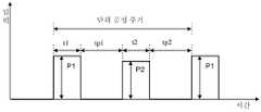
도 1은 종래의 미국특허 제4,413,022호에 개시된 바 있는 ALD법을 이용한 박막 형성방법을 설명하기 위한 그래프이다.1 is a graph for explaining a method of forming a thin film using the ALD method disclosed in the prior art US Patent No. 4,413,022.
도 1을 참조하면, 제1 반응기체를 반응실로 유입하여 압력 P1의 상태에서 t1의 시간 동안 유지되도록 한다. 이어서, 제1 반응기체의 유입을 중단시키고, 실리 콘 기판 상에 제1 반응기체가 단층막 이상으로 흡착되는 것을 방지하고 반응실의 미반응한 잔류 기체를 제거하기 위하여 Ar 또는 He과 같은 불활성 기체를 tp1의 시간 동안 반응실로 유입한다.Referring to Figure 1, the first reactor is introduced into the reaction chamber to be maintained for a time t1 in the state of the pressure P1. Then, an inert gas such as Ar or He is used to stop the inflow of the first reactor body, to prevent the first reactor body from adsorbing onto the silicon substrate beyond the monolayer film and to remove the unreacted residual gas from the reaction chamber. Is introduced into the reaction chamber for a time of tp1.
다음에, 환원 기체 또는 제2 반응기체를 반응실로 유입하여 압력 P2의 상태에서 t2의 시간 동안 유지되도록 한다. 이어서, 환원 기체 또는 제2 반응기체의 유입을 중단시키고, 반응실의 미반응한 잔류 기체를 제거하기 위하여 Ar 또는 He과 같은 불활성 기체를 tp2의 시간 동안 반응실로 유입한다.Next, a reducing gas or a second reactor is introduced into the reaction chamber so as to be maintained for a time t2 at the state of the pressure P2. Then, the inlet of reducing gas or the second reactor is stopped and an inert gas such as Ar or He is introduced into the reaction chamber for a time of tp 2 to remove unreacted residual gas from the reaction chamber.
이때, 상기 공정 중에서 제1 및 제2 반응기체에 대한 실리콘 기판의 노출 시간은 최소화가 요구되므로 저압에서의 공정 진행이 필요하다. 한편, 반응실의 잔류 기체를 제거하기 위한 불활성 기체는 충분한 시간 동안 유입시켜야 한다.At this time, the exposure time of the silicon substrate to the first and second reactors in the process is required to minimize the process at low pressure. On the other hand, an inert gas for removing residual gas in the reaction chamber should be introduced for a sufficient time.
도 1과 같은 방법을 이용하여 알루미나(Alumina: Al2O3) 박막을 형성시킨 예가 아래와 같다.An example of forming an alumina (Alumina: Al2 O3 ) thin film using the same method as in FIG. 1 is as follows.
도 1과 결부하여 설명하면, 증착 온도 370℃에서 트리메틸알루미늄(Tri-Methyl-Aluminum, Al(CH3)3, 이하 'TMA')을 반응실로 유입하여 압력 230mTorr(P1)의 상태에서 1초(t1) 동안 유지되도록 한다. 이어서, TMA의 유입을 중단시키고, 실리콘 기판 상에 TMA가 단층막 이상으로 흡착되는 것을 방지하고 반응실의 미반응한 잔류 기체를 제거하기 위하여 Ar을 14초(tp1) 동안 반응실로 유입한다.Referring to FIG. 1, tri-methyl-aluminum (Al (CH3 )3 , hereinafter 'TMA') is introduced into the reaction chamber at a deposition temperature of 370 ° C. for 1 second at a pressure of 230 mTorr (P1 ). to be held for (t1 ). Subsequently, Ar is introduced into the reaction chamber for 14 seconds (tp1 ) to stop the inflow of TMA, to prevent the TMA from adsorbing onto the silicon substrate and to remove unreacted residual gas from the reaction chamber.
다음에, 초순수(Distilled Water, 이하 'DIW')의 수증기를 반응실로 유입하 여 압력 200mTorr(P2)의 상태에서 1초(t2) 동안 유지되도록 한다. 이어서, TMA의 유입을 중단시키고, 반응실의 미반응한 잔류 기체를 제거하기 위하여 Ar을 14초(tp2) 동안 반응실로 유입한다.Next, water vapor of distilled water (hereinafter referred to as 'DIW') is introduced into the reaction chamber and maintained at a pressure of 200 mTorr (P2 ) for 1 second (t2 ). Then, the inflow of TMA is stopped and Ar is introduced into the reaction chamber for 14 seconds (tp2 ) to remove unreacted residual gas from the reaction chamber.
상기의 공정에서는 1회 주기 즉, 30초 동안의 실시에 의한 알루미나 막의 증착 두께가 0.3nm 정도이다. 따라서, 알루미나 박막을 10nm 정도의 두께로 증착하기 위해서는 이러한 주기를 34회 정도 반복하여야 하므로, 약 1000초의 시간이 소요된다. 이와 같이 ALD법에 의할 경우는 CVD법을 이용하는 경우보다 단위 시간당 생산성이 크게 떨어지게 된다. 그러므로 이를 보완하기 위해서는 많은 수의 집합형 설비(Cluster System)의 도입이 필요하며, 반도체 장치 등의 제조 원가 상승 요인으로 작용하게 된다.
In the above process, the deposition thickness of the alumina film in one cycle, that is, 30 seconds, is about 0.3 nm. Therefore, in order to deposit the alumina thin film with a thickness of about 10 nm, this cycle must be repeated about 34 times, which takes about 1000 seconds. As described above, in the case of the ALD method, the productivity per unit time is significantly lower than that in the CVD method. Therefore, in order to compensate for this, it is necessary to introduce a large number of cluster systems, which increases the manufacturing cost of semiconductor devices.
따라서, 본 발명이 이루고자 하는 기술적 과제는 단위 공정 주기 소요 시간을 단축함으로써 생산성을 향상시키는 원자층 증착법을 이용한 박막 형성방법을 제공하는 데 있다.
Accordingly, an aspect of the present invention is to provide a method for forming a thin film using an atomic layer deposition method which improves productivity by shortening a unit process cycle time required.
상기 기술적 과제들을 달성하기 위한 본 발명의 ALD법을 이용한 박막 형성방법은, 실리콘 기판을 반응실에 위치시키는 제1 단계와; 상기 반응실로 제1 반응기 체를 운반기체와 더불어 유입하여 상기 실리콘 기판 상에 상기 제1 반응기체를 화학 흡착시키는 제2 단계와; 상기 제2 단계에서 보다 더 낮게 상기 반응실의 압력이 유지되도록, 상기 제2 단계를 중지함과 동시에 상기 반응실로 제2 반응기체를 1차 유입하여, 상기 실리콘 기판 상에 상기 제2 반응기체를 화학 흡착시킴과 동시에 상기 제1 반응기체중 미반응 잔류 기체를 제거하는 제3 단계와; 상기 제2 단계보다 더 높게 상기 반응실의 압력이 유지되도록 상기 제2 반응기체를 상기 반응실로 2차 유입하여, 상기 제2 반응기체를 화학 흡착시키는 제4 단계를 포함하는 것을 특징으로 한다.According to an aspect of the present invention, there is provided a method of forming a thin film using the ALD method, the method including: placing a silicon substrate in a reaction chamber; A second step of introducing the first reactor body into the reaction chamber together with a carrier gas to chemisorb the first reactor body onto the silicon substrate; In order to maintain the pressure in the reaction chamber lower than in the second step, the second reactor is first introduced into the reaction chamber at the same time as the second step is stopped, so that the second reactor is placed on the silicon substrate. Chemically adsorbing and simultaneously removing unreacted residual gas in the first reactor body; And secondly introducing the second reactor body into the reaction chamber so that the pressure of the reaction chamber is maintained higher than the second step, and chemically adsorbing the second reactor body.
이 때, 상기 제3 단계에 있어서의 상기 제2 반응기체가 운반기체와 더불어 유입되는 것이 바람직하며, 상기 제4 단계에 있어서의 상기 제2 반응기체가 운반기체와 더불어 유입되는 것이 바람직하다.At this time, it is preferable that the second reactor body in the third step is introduced together with the carrier gas, and the second reactor body in the fourth step is preferably introduced together with the carrier gas.
한편, 증착시키고자 하는 박막이 두꺼울 경우에는 상기 제2 단계 내지 제4 단계를 순차적으로 2회 이상 반복할 수 도 있다.
Meanwhile, when the thin film to be deposited is thick, the second to fourth steps may be repeated two or more times in sequence.
이하, 첨부한 도면을 참조하여 본 발명의 바람직한 실시예들을 상세히 설명한다.Hereinafter, exemplary embodiments of the present invention will be described in detail with reference to the accompanying drawings.
도 2는 본 발명에 의한 ALD법을 이용한 박막 형성방법을 설명하기 위한 그래프이다.2 is a graph for explaining a method of forming a thin film using the ALD method according to the present invention.
[실시예 1]Example 1
ALD법을 이용한 TiN 박막을 형성하는 방법을 도 2와 결부하여 설명하면 다 음과 같다. A method of forming a TiN thin film using the ALD method will be described with reference to FIG. 2 as follows.
우선, 산화막이 증착된 실리콘 기판을 반응실에 위치시킨다. 그 다음, 반응실의 온도를 500℃로 유지하고, 반응실이 0.04Torr∼0.06Torr의 압력(P1')으로 0.8초∼1.2초(t1') 동안 유지되도록 제1 반응기체 예컨대, TiCl4와 함께 운반기체 예컨대, Ar를 80∼120sccm의 유량으로 유입하여 TiClX를 실리콘 기판 상에 화학 흡착시킨다. 불필요한 물리 흡착 층이 억제되도록 가능한 한 저압에서 단시간 동안 이러한 화학 흡착을 진행시킨다. 이때, 불활성 기체를 함께 유입하는 이유는, 반응실에 잔류하는 미반응 기체가 후속의 제2 반응기체와 반응할 수 있는 확률을 최소화하기 위해서 이다. 특히, 제1 반응기체가 점성이 있는 경우에는 불활성 기체가 제1 반응기체의 점도를 희석시키는 역할도 하므로 제1 반응기체가 반응실에 흡착되는 것이 방지되어 더욱 유용하다.First, a silicon substrate on which an oxide film is deposited is placed in a reaction chamber. Then, the temperature of the reaction chamber is maintained at 500 ° C., and the first reactor body such as TiCl is maintained for 0.8 seconds to 1.2 seconds (t1 ') at a pressure (P1 ') of 0.04 Torr to 0.06 Torr.4 together with a carrier gas, such as Ar, is introduced at a flow rate of 80 to 120 sccm to chemisorb TiClX onto the silicon substrate. This chemisorption proceeds for as short a time as possible so that unnecessary physical adsorption layers are suppressed. At this time, the reason for introducing the inert gas together is to minimize the probability that the unreacted gas remaining in the reaction chamber can react with the subsequent second reactor body. In particular, when the first reactor is viscous, the inert gas also serves to dilute the viscosity of the first reactor, which is more useful because the first reactor is prevented from adsorbing to the reaction chamber.
이어서, 반응실의 압력이 TiCl4 및 Ar에 의해 형성된 압력 보다 낮은 0.008Torr∼0.012Torr의 압력(P2')으로 3초∼5초(t2') 동안 유지되도록 제2 반응기체 예컨대, NH3를 240∼360sccm의 유량으로 유입하여 실리콘 기판 상에 NH3의 질소 성분을 화학 흡착시켜 TiN 박막을 형성시키는 동시에 이미 유입된 TiCl4중 실리콘 기판 상에 흡착하지 않은 잔류 기체를 제거한다.Subsequently, the second reactor body such as NH is maintained such that the pressure in the reaction chamber is maintained for 3 seconds to 5 seconds (t2 ') at a pressure (P2 ') of 0.008 Torr to 0.012 Torr lower than the pressure formed by TiCl4 and Ar.3 is introduced at a flow rate of 240 to 360 sccm to chemisorb nitrogen components of NH3 on the silicon substrate to form a TiN thin film, and remove residual gas not adsorbed on the silicon substrate of TiCl4 already introduced.
계속해서, 반응실의 압력이 TiCl4 및 Ar에 의해 형성된 압력 보다 높은 0.2Torr∼0.3Torr의 압력(P2'')으로 8초∼12초(t2'') 동안 유지되도록 제2 반응기체 예컨대, NH3를 240∼360sccm의 유량으로 유입하여 실리콘 기판 상에 NH3의 질소 성분이 조밀하게 화학 흡착되도록 하여 결과적으로 TiN 박막을 형성시킨다.Subsequently, the second reactor body is maintained such that the pressure in the reaction chamber is maintained for 8 seconds to 12 seconds (t2 '') at a pressure (P2 '') of 0.2 Torr to 0.3 Torr higher than the pressure formed by TiCl4 and Ar. For example, NH3 is introduced at a flow rate of 240 to 360 sccm so that the nitrogen component of NH3 is densely chemisorbed on the silicon substrate, resulting in a TiN thin film.
한편, 열 화학 기상 증착법(Thermal Chemical Vapor Deposition)에서 가장 보편적으로 적용되는 샤워 헤드(Shower Head)를 사용하여 기체를 주입할 경우, 처음에는 불순물 미립자(Particle)의 발생 량이 미미하나 반응기체에 대한 샤워 헤드의 노출 빈도수가 점차 증가됨에 따라 불완전한 반응이 샤워 헤드 내에서 발생하게 되어 원하지 않는 불순물 미립자가 증가하게 된다. 따라서, 이를 방지하기 위해 종래의 샤워 헤드 대신에 하나 이상의 분사구를 갖는 다중 분사기를 이용하여 TiCl4, Ar 및 NH3를 각각 유입하는 것이 바람직하다.On the other hand, when gas is injected using a shower head, which is most commonly used in thermal chemical vapor deposition, the amount of impurity particles is initially generated but the shower head for the reactant is small. As the frequency of exposure increases, an incomplete reaction occurs in the shower head, causing an increase in unwanted impurity particulates. Therefore, in order to prevent this, it is preferable to introduce TiCl4 , Ar, and NH3 , respectively, using a multi-injector having one or more injection holes instead of the conventional shower head.
상기와 같이 TiN 박막을 증착한 결과, 박막 증착 속도는 1공정 주기당 11.8∼18.2초의 시간이 소요되며, 증착된 박막의 두께는 1공정 주기당 1.2∼1.8nm로 형성된다. 또한, 접촉구 바닥 직경이 0.3㎛, 접촉구경비가 3.8일 때 90% 이상의 단차피복성(Step Coverage)을 얻을 수 있었고, 비저항은 130μΩ·㎝이다.As a result of depositing the TiN thin film as described above, the thin film deposition rate takes 11.8 to 18.2 seconds per process cycle, and the thickness of the deposited thin film is formed to 1.2 to 1.8 nm per process cycle. In addition, when the contact bottom diameter was 0.3 µm and the contact diameter ratio was 3.8, step coverage of 90% or more was obtained, and the specific resistance was 130 µΩ · cm.
한편, 박막내 염소 성분이 함유될 경우에는, 박막내 함유되어 있는 염소가 대기중의 수분과 반응하여 강산인 HCl이 형성되고, 이로 인해 증착된 박막 및 그 박막 위에 증착되는 알루미늄과 같은 금속 배선이 손상되어 금속 배선의 신뢰성이 저하되게 된다. 본 발명에 의해 증착된 상기 TiN 박막은, 박막내 염소 농도가 XPS(X-Ray Photoelectron Spectroscopy)로 측정시 그 측정 한계 이하로 나타나므 로, 금속 배선에 대한 신뢰성을 증대시킬 뿐만 아니라 금속 배선을 더욱 미세화 시킬 수 있다.On the other hand, when the chlorine component is contained in the thin film, chlorine contained in the thin film reacts with moisture in the air to form HCl, which is a strong acid, and thus the deposited thin film and metal wiring such as aluminum deposited on the thin film are formed. It is damaged and the reliability of a metal wiring falls. The TiN thin film deposited by the present invention, since the chlorine concentration in the thin film is measured below the measurement limit when measured by X-Ray Photoelectron Spectroscopy (XPS), not only increases the reliability of the metal wiring but also improves the metal wiring. It can be refined.
[실시예 2]Example 2
ALD법을 이용한 알루미나(Alumina: Al2O3) 박막을 형성하는 방법을 도 2와 결부하여 설명하면 다음과 같다.A method of forming an alumina (Alumina: Al2 O3 ) thin film using the ALD method will be described with reference to FIG. 2 as follows.
우선, 산화막이 증착된 실리콘 기판을 반응실에 위치시킨다. 그 다음, 반응실의 온도를 350℃로 유지하고, 반응실이 0.2Torr∼0.3Torr의 압력(P1')으로 0.8초∼1.2초(t1') 동안 유지되도록 TMA와 더불어 Ar을 80∼120sccm의 유량으로 유입하여 TMA를 실리콘 기판 상에 화학 흡착시킨다.First, a silicon substrate on which an oxide film is deposited is placed in a reaction chamber. Then, the temperature of the reaction chamber is maintained at 350 ° C., and the Ar is 80 to 80 seconds with TMA so that the reaction chamber is maintained at a pressure P1 ′ of 0.2 Torr to 0.3 Torr for 0.8 sec to 1.2 sec (t1 '). The TMA is chemisorbed onto the silicon substrate by flowing at a flow rate of 120 sccm.
이어서, 반응실의 압력이 TMA 및 Ar에 의해 형성된 압력 보다 낮은 0.04Torr∼0.06Torr의 압력(P2')으로 3.2초∼4.8초(t2') 동안 유지되도록 DIW 및 Ar을 80∼120sccm의 유량으로 유입하여 DIW의 산소 성분을 실리콘 기판 상에 화학 흡착시켜 알루미나 박막을 형성시키는 동시에 이미 유입된 TMA중 실리콘 기판 상에 흡착되지 않은 잔류 기체를 제거한다. 이때, 불활성 기체를 함께 유입하는 이유는, 실리콘 기판 상에 화학 흡착된 TMA의 단층막 상에 존재하는 물리 흡착 층에 대하여 불활성 기체에 의한 충돌을 유발하여 TMA의 미반응된 잔류 기체의 제거 효율을 높이기 위해서 이다.Subsequently, DIW and Ar were maintained at 80 to 120 sccm so that the pressure in the reaction chamber was maintained for 3.2 seconds to 4.8 seconds (t2 ') at a pressure (P2 ') of 0.04 Torr to 0.06 Torr lower than the pressure formed by TMA and Ar. The oxygen content of the DIW is chemically adsorbed on the silicon substrate to form a thin film of alumina while removing residual gas that is not adsorbed on the silicon substrate of the already introduced TMA. At this time, the inert gas is introduced together, causing an impingement by the inert gas to the physical adsorption layer present on the monolayer film of the TMA chemisorbed on the silicon substrate to remove the unreacted residual gas of the TMA To increase.
계속해서, 반응실의 압력이 TMA 및 Ar에 의해 형성된 압력 보다 높은 0.2Torr∼0.3Torr의 압력(P2'')으로 4초∼6초(t2'') 동안 유지되도록 DIW 및 Ar를 80∼120sccm의 유량으로 유입하여 DIW의 산소 성분을 실리콘 기판 상에 조밀하게 화학 흡착시켜 결과적으로 알루미나 박막을 형성시킨다. 이때, 불활성 기체를 함께 유입하는 이유는 DIW의 물리 흡착을 방지하거나 최소화하기 위해서 이다.Subsequently, DIW and Ar were set to 80 so that the pressure in the reaction chamber was maintained for 4 seconds to 6 seconds (t2 '') at a pressure (P2 '') of 0.2 Torr to 0.3 Torr higher than the pressure formed by TMA and Ar. Flowing at a flow rate of ˜120 sccm, the oxygen component of DIW is densely chemisorbed onto the silicon substrate, resulting in a thin alumina film. At this time, the reason for introducing the inert gas together is to prevent or minimize physical adsorption of the DIW.
한편, 실시예 1의 경우처럼, TMA, Ar, 및 DIW는 각각 하나 이상의 분사구를 갖는 다중 분사기를 이용하여 유입하는 것이 바람직하다.On the other hand, as in the case of Example 1, TMA, Ar, and DIW is preferably introduced by using a multi-injector having one or more injection holes.
상기와 같이 알루미나 박막을 증착한 결과, 박막 증착 속도는 1공정 주기당 8∼12초의 시간이 소요되며, 증착된 박막의 두께는 1공정 주기당 0.17∼0.25nm로 형성된다. 또한, 반사율(Reflective Index)은 633nm 파장에서는 실리콘 기판에 대해서는 1.6, 실리콘 산화막(SiO2)에 대해서는 1.62이다. 접촉구 바닥 직경이 0.3㎛, 접촉구경비가 3.8일 때 90% 이상의 단차피복성(Step Coverage)을 얻을 수 있다. 한편, 박막내 탄소의 농도는 XPS로 측정시 그 측정 한계 이하로 나타나므로 박막의 밀도 및 전기적인 특성이 개선되었다.As a result of depositing the alumina thin film as described above, the thin film deposition rate takes 8 to 12 seconds per process cycle, and the thickness of the deposited thin film is formed to be 0.17 to 0.25 nm per process cycle. The reflective index is 1.6 for the silicon substrate and 1.62 for the silicon oxide film (SiO2 ) at 633 nm. When the contact bottom diameter is 0.3㎛ and the contact diameter ratio is 3.8, more than 90% of step coverage can be obtained. On the other hand, since the concentration of carbon in the thin film is measured below the measurement limit when measured by XPS, the density and electrical properties of the thin film were improved.
상기의 결과에서, 1공정 주기당 예컨대, 12초 동안 최소 0.17nm의 두께로 알루미나 박막이 형성된다. 따라서, 알루미나 박막을 10nm 정도의 두께로 증착하기 위해서는 이러한 공정을 60회 정도 반복하면 되므로 720초의 시간이 소요된다. 이와 같이, 본 발명에 의할 경우 종래의 ALD법에 의해 알루미나 박막을 생산하는 경우보다 단위 시간당 생산성이 크게 향상된다.
As a result of the above, an alumina thin film is formed with a thickness of at least 0.17 nm, for example, for 12 seconds per one processing cycle. Therefore, in order to deposit the alumina thin film with a thickness of about 10 nm, this process may be repeated about 60 times, which takes 720 seconds. As described above, according to the present invention, the productivity per unit time is greatly improved compared with the case of producing an alumina thin film by the conventional ALD method.
상술한 바와 같이 본 발명의 ALD법을 이용한 박막 형성 방법에 의하면, 종래보다 단위 공정 주기당 단계 수를 반으로 줄일 수 있으므로 단위 시간당 생산성을 향상시킬 수 있다.As described above, according to the thin film forming method using the ALD method of the present invention, since the number of steps per unit process cycle can be reduced by half, the productivity per unit time can be improved.
또한, 박막내 잔류 염소 농도를 현저히 감소시킴으로써 플라즈마(Plasma) 처리와 같은 별도의 추가 공정이 필요 없을 뿐만 아니라, 금속 배선에 대한 신뢰성을 증대시키고 금속 배선을 더욱 미세화 할 수 있다.In addition, by significantly reducing the residual chlorine concentration in the thin film, a separate additional process such as plasma treatment is not required, and the reliability of the metal wiring can be increased and the metal wiring can be further refined.
나아가, 종래보다 낮은 온도에서 증착이 가능하고, 금속-유기 반응기체를 사용할 때 박막내 함유되는 탄소의 농도가 현저히 감소되므로 증착되는 박막의 밀도 및 전기적 특성이 개선된다.Furthermore, deposition is possible at a lower temperature than before, and the density and electrical properties of the deposited thin film are improved because the concentration of carbon contained in the thin film is significantly reduced when using a metal-organic reactor.
본 발명은 상기 실시예들에만 한정되지 않으며, 본 발명의 기술적 사상 내에서 당 분야의 통상의 지식을 가진 자에 의해 많은 변형이 가능함은 명백하다.
The present invention is not limited to the above embodiments, and it is apparent that many modifications are possible by those skilled in the art within the technical spirit of the present invention.
Claims (12)
Translated fromKoreanPriority Applications (2)
| Application Number | Priority Date | Filing Date | Title |
|---|---|---|---|
| KR1020000031040AKR100647442B1 (en) | 2000-06-07 | 2000-06-07 | Thin film formation method using atomic layer deposition |
| US09/874,686US20010050039A1 (en) | 2000-06-07 | 2001-06-05 | Method of forming a thin film using atomic layer deposition method |
Applications Claiming Priority (1)
| Application Number | Priority Date | Filing Date | Title |
|---|---|---|---|
| KR1020000031040AKR100647442B1 (en) | 2000-06-07 | 2000-06-07 | Thin film formation method using atomic layer deposition |
Publications (2)
| Publication Number | Publication Date |
|---|---|
| KR20010110531A KR20010110531A (en) | 2001-12-13 |
| KR100647442B1true KR100647442B1 (en) | 2006-11-17 |
Family
ID=19671304
Family Applications (1)
| Application Number | Title | Priority Date | Filing Date |
|---|---|---|---|
| KR1020000031040AExpired - Fee RelatedKR100647442B1 (en) | 2000-06-07 | 2000-06-07 | Thin film formation method using atomic layer deposition |
Country Status (2)
| Country | Link |
|---|---|
| US (1) | US20010050039A1 (en) |
| KR (1) | KR100647442B1 (en) |
Cited By (1)
| Publication number | Priority date | Publication date | Assignee | Title |
|---|---|---|---|---|
| KR101815736B1 (en)* | 2014-08-12 | 2018-01-05 | 도쿄엘렉트론가부시키가이샤 | Processing apparatus |
Families Citing this family (63)
| Publication number | Priority date | Publication date | Assignee | Title |
|---|---|---|---|---|
| US6974766B1 (en) | 1998-10-01 | 2005-12-13 | Applied Materials, Inc. | In situ deposition of a low κ dielectric layer, barrier layer, etch stop, and anti-reflective coating for damascene application |
| US6620723B1 (en) | 2000-06-27 | 2003-09-16 | Applied Materials, Inc. | Formation of boride barrier layers using chemisorption techniques |
| US7101795B1 (en) | 2000-06-28 | 2006-09-05 | Applied Materials, Inc. | Method and apparatus for depositing refractory metal layers employing sequential deposition techniques to form a nucleation layer |
| US6551929B1 (en) | 2000-06-28 | 2003-04-22 | Applied Materials, Inc. | Bifurcated deposition process for depositing refractory metal layers employing atomic layer deposition and chemical vapor deposition techniques |
| US6936538B2 (en) | 2001-07-16 | 2005-08-30 | Applied Materials, Inc. | Method and apparatus for depositing tungsten after surface treatment to improve film characteristics |
| US7405158B2 (en) | 2000-06-28 | 2008-07-29 | Applied Materials, Inc. | Methods for depositing tungsten layers employing atomic layer deposition techniques |
| WO2002070142A1 (en)* | 2000-12-06 | 2002-09-12 | Angstron Systems, Inc. | Method and apparatus for improved temperature control in atomic layer deposition |
| US6630201B2 (en) | 2001-04-05 | 2003-10-07 | Angstron Systems, Inc. | Adsorption process for atomic layer deposition |
| US6800173B2 (en) | 2000-12-15 | 2004-10-05 | Novellus Systems, Inc. | Variable gas conductance control for a process chamber |
| US20020144786A1 (en)* | 2001-04-05 | 2002-10-10 | Angstron Systems, Inc. | Substrate temperature control in an ALD reactor |
| US6596643B2 (en) | 2001-05-07 | 2003-07-22 | Applied Materials, Inc. | CVD TiSiN barrier for copper integration |
| US6828218B2 (en)* | 2001-05-31 | 2004-12-07 | Samsung Electronics Co., Ltd. | Method of forming a thin film using atomic layer deposition |
| US6849545B2 (en)* | 2001-06-20 | 2005-02-01 | Applied Materials, Inc. | System and method to form a composite film stack utilizing sequential deposition techniques |
| US20030198754A1 (en)* | 2001-07-16 | 2003-10-23 | Ming Xi | Aluminum oxide chamber and process |
| JP2005504885A (en) | 2001-07-25 | 2005-02-17 | アプライド マテリアルズ インコーポレイテッド | Barrier formation using a novel sputter deposition method |
| US20090004850A1 (en) | 2001-07-25 | 2009-01-01 | Seshadri Ganguli | Process for forming cobalt and cobalt silicide materials in tungsten contact applications |
| US9051641B2 (en) | 2001-07-25 | 2015-06-09 | Applied Materials, Inc. | Cobalt deposition on barrier surfaces |
| US8110489B2 (en) | 2001-07-25 | 2012-02-07 | Applied Materials, Inc. | Process for forming cobalt-containing materials |
| US20030029715A1 (en) | 2001-07-25 | 2003-02-13 | Applied Materials, Inc. | An Apparatus For Annealing Substrates In Physical Vapor Deposition Systems |
| US7049226B2 (en) | 2001-09-26 | 2006-05-23 | Applied Materials, Inc. | Integration of ALD tantalum nitride for copper metallization |
| US6936906B2 (en) | 2001-09-26 | 2005-08-30 | Applied Materials, Inc. | Integration of barrier layer and seed layer |
| US6916398B2 (en) | 2001-10-26 | 2005-07-12 | Applied Materials, Inc. | Gas delivery apparatus and method for atomic layer deposition |
| US7081271B2 (en) | 2001-12-07 | 2006-07-25 | Applied Materials, Inc. | Cyclical deposition of refractory metal silicon nitride |
| AU2003238853A1 (en) | 2002-01-25 | 2003-09-02 | Applied Materials, Inc. | Apparatus for cyclical deposition of thin films |
| US6998014B2 (en) | 2002-01-26 | 2006-02-14 | Applied Materials, Inc. | Apparatus and method for plasma assisted deposition |
| US6911391B2 (en) | 2002-01-26 | 2005-06-28 | Applied Materials, Inc. | Integration of titanium and titanium nitride layers |
| US6833161B2 (en) | 2002-02-26 | 2004-12-21 | Applied Materials, Inc. | Cyclical deposition of tungsten nitride for metal oxide gate electrode |
| US7439191B2 (en)* | 2002-04-05 | 2008-10-21 | Applied Materials, Inc. | Deposition of silicon layers for active matrix liquid crystal display (AMLCD) applications |
| US6720027B2 (en) | 2002-04-08 | 2004-04-13 | Applied Materials, Inc. | Cyclical deposition of a variable content titanium silicon nitride layer |
| US6846516B2 (en) | 2002-04-08 | 2005-01-25 | Applied Materials, Inc. | Multiple precursor cyclical deposition system |
| US7279432B2 (en)* | 2002-04-16 | 2007-10-09 | Applied Materials, Inc. | System and method for forming an integrated barrier layer |
| US7041335B2 (en) | 2002-06-04 | 2006-05-09 | Applied Materials, Inc. | Titanium tantalum nitride silicide layer |
| US6838125B2 (en) | 2002-07-10 | 2005-01-04 | Applied Materials, Inc. | Method of film deposition using activated precursor gases |
| US20040013803A1 (en)* | 2002-07-16 | 2004-01-22 | Applied Materials, Inc. | Formation of titanium nitride films using a cyclical deposition process |
| US6915592B2 (en) | 2002-07-29 | 2005-07-12 | Applied Materials, Inc. | Method and apparatus for generating gas to a processing chamber |
| US7150789B2 (en) | 2002-07-29 | 2006-12-19 | Micron Technology, Inc. | Atomic layer deposition methods |
| US6753271B2 (en)* | 2002-08-15 | 2004-06-22 | Micron Technology, Inc. | Atomic layer deposition methods |
| US6890596B2 (en)* | 2002-08-15 | 2005-05-10 | Micron Technology, Inc. | Deposition methods |
| US20040036129A1 (en)* | 2002-08-22 | 2004-02-26 | Micron Technology, Inc. | Atomic layer deposition of CMOS gates with variable work functions |
| US6967154B2 (en) | 2002-08-26 | 2005-11-22 | Micron Technology, Inc. | Enhanced atomic layer deposition |
| US6673701B1 (en)* | 2002-08-27 | 2004-01-06 | Micron Technology, Inc. | Atomic layer deposition methods |
| US6821563B2 (en)* | 2002-10-02 | 2004-11-23 | Applied Materials, Inc. | Gas distribution system for cyclical layer deposition |
| US6905737B2 (en) | 2002-10-11 | 2005-06-14 | Applied Materials, Inc. | Method of delivering activated species for rapid cyclical deposition |
| US7262133B2 (en) | 2003-01-07 | 2007-08-28 | Applied Materials, Inc. | Enhancement of copper line reliability using thin ALD tan film to cap the copper line |
| US7244683B2 (en) | 2003-01-07 | 2007-07-17 | Applied Materials, Inc. | Integration of ALD/CVD barriers with porous low k materials |
| US20040134427A1 (en)* | 2003-01-09 | 2004-07-15 | Derderian Garo J. | Deposition chamber surface enhancement and resulting deposition chambers |
| US20040198069A1 (en) | 2003-04-04 | 2004-10-07 | Applied Materials, Inc. | Method for hafnium nitride deposition |
| US7192849B2 (en)* | 2003-05-07 | 2007-03-20 | Sensor Electronic Technology, Inc. | Methods of growing nitride-based film using varying pulses |
| US7211508B2 (en) | 2003-06-18 | 2007-05-01 | Applied Materials, Inc. | Atomic layer deposition of tantalum based barrier materials |
| US20050252449A1 (en) | 2004-05-12 | 2005-11-17 | Nguyen Son T | Control of gas flow and delivery to suppress the formation of particles in an MOCVD/ALD system |
| US8323754B2 (en) | 2004-05-21 | 2012-12-04 | Applied Materials, Inc. | Stabilization of high-k dielectric materials |
| US7429402B2 (en) | 2004-12-10 | 2008-09-30 | Applied Materials, Inc. | Ruthenium as an underlayer for tungsten film deposition |
| US8486845B2 (en)* | 2005-03-21 | 2013-07-16 | Tokyo Electron Limited | Plasma enhanced atomic layer deposition system and method |
| US7473637B2 (en)* | 2005-07-20 | 2009-01-06 | Micron Technology, Inc. | ALD formed titanium nitride films |
| TWI332532B (en) | 2005-11-04 | 2010-11-01 | Applied Materials Inc | Apparatus and process for plasma-enhanced atomic layer deposition |
| US7709402B2 (en) | 2006-02-16 | 2010-05-04 | Micron Technology, Inc. | Conductive layers for hafnium silicon oxynitride films |
| US7798096B2 (en) | 2006-05-05 | 2010-09-21 | Applied Materials, Inc. | Plasma, UV and ion/neutral assisted ALD or CVD in a batch tool |
| US7521379B2 (en) | 2006-10-09 | 2009-04-21 | Applied Materials, Inc. | Deposition and densification process for titanium nitride barrier layers |
| US7659158B2 (en) | 2008-03-31 | 2010-02-09 | Applied Materials, Inc. | Atomic layer deposition processes for non-volatile memory devices |
| US20100062149A1 (en) | 2008-09-08 | 2010-03-11 | Applied Materials, Inc. | Method for tuning a deposition rate during an atomic layer deposition process |
| US8491967B2 (en) | 2008-09-08 | 2013-07-23 | Applied Materials, Inc. | In-situ chamber treatment and deposition process |
| JP6017396B2 (en)* | 2012-12-18 | 2016-11-02 | 東京エレクトロン株式会社 | Thin film forming method and thin film forming apparatus |
| JP6485536B1 (en)* | 2017-12-28 | 2019-03-20 | 株式会社Sumco | Epitaxial wafer manufacturing apparatus and manufacturing method |
Citations (4)
| Publication number | Priority date | Publication date | Assignee | Title |
|---|---|---|---|---|
| US5879459A (en)* | 1997-08-29 | 1999-03-09 | Genus, Inc. | Vertically-stacked process reactor and cluster tool system for atomic layer deposition |
| KR20000013654A (en)* | 1998-08-12 | 2000-03-06 | 윤종용 | Capacitor having an al2o3/aln mixed dielectric layer by using an atomic layer deposition and a manufacturing method thereof |
| KR20000015134A (en)* | 1998-08-27 | 2000-03-15 | 윤종용 | GATE ELECTRODE HAVING TiN ELECTRODE LAYER AND METHOD THEREOF |
| KR20000017682A (en)* | 1999-02-25 | 2000-04-06 | 정수홍 | Atomic layer deposition apparatus |
Family Cites Families (1)
| Publication number | Priority date | Publication date | Assignee | Title |
|---|---|---|---|---|
| KR100297719B1 (en)* | 1998-10-16 | 2001-08-07 | 윤종용 | Method for manufacturing thin film |
- 2000
- 2000-06-07KRKR1020000031040Apatent/KR100647442B1/ennot_activeExpired - Fee Related
- 2001
- 2001-06-05USUS09/874,686patent/US20010050039A1/ennot_activeAbandoned
Patent Citations (4)
| Publication number | Priority date | Publication date | Assignee | Title |
|---|---|---|---|---|
| US5879459A (en)* | 1997-08-29 | 1999-03-09 | Genus, Inc. | Vertically-stacked process reactor and cluster tool system for atomic layer deposition |
| KR20000013654A (en)* | 1998-08-12 | 2000-03-06 | 윤종용 | Capacitor having an al2o3/aln mixed dielectric layer by using an atomic layer deposition and a manufacturing method thereof |
| KR20000015134A (en)* | 1998-08-27 | 2000-03-15 | 윤종용 | GATE ELECTRODE HAVING TiN ELECTRODE LAYER AND METHOD THEREOF |
| KR20000017682A (en)* | 1999-02-25 | 2000-04-06 | 정수홍 | Atomic layer deposition apparatus |
Cited By (1)
| Publication number | Priority date | Publication date | Assignee | Title |
|---|---|---|---|---|
| KR101815736B1 (en)* | 2014-08-12 | 2018-01-05 | 도쿄엘렉트론가부시키가이샤 | Processing apparatus |
Also Published As
| Publication number | Publication date |
|---|---|
| US20010050039A1 (en) | 2001-12-13 |
| KR20010110531A (en) | 2001-12-13 |
Similar Documents
| Publication | Publication Date | Title |
|---|---|---|
| KR100647442B1 (en) | Thin film formation method using atomic layer deposition | |
| US7077904B2 (en) | Method for atomic layer deposition (ALD) of silicon oxide film | |
| US6468924B2 (en) | Methods of forming thin films by atomic layer deposition | |
| KR100539274B1 (en) | Method for depositing cobalt layer | |
| US6800542B2 (en) | Method for fabricating ruthenium thin layer | |
| TWI394203B (en) | Method for forming titanium nitride film by atomic layer deposition method | |
| JP4974676B2 (en) | Formation method of barrier film | |
| US20100227476A1 (en) | Atomic layer deposition processes | |
| US8372481B2 (en) | Methods of forming material on a substrate, and a method of forming a field effect transistor gate oxide on a substrate | |
| KR20010114050A (en) | Method of forming a Al2O3 layer in a semiconductor device | |
| KR100519376B1 (en) | Method for Forming Barrier Layer of Semiconductor Device | |
| KR20020001376A (en) | Method of forming a Al2O3 layer in a semiconductor device | |
| US6951813B2 (en) | Methods of forming metal-containing layers including a metal bonded to halogens and trialkylaluminum | |
| US7538046B2 (en) | Method of cleaning semiconductor device fabrication apparatus | |
| KR100510473B1 (en) | Method for forming upper electrode of a capacitor using ALD | |
| JPH066789B2 (en) | Deposition method of borophosphosilicate glass | |
| JPS62287513A (en) | Transparent conducting film and manufacture thereof | |
| US6232234B1 (en) | Method of reducing in film particle number in semiconductor manufacture | |
| JP3189767B2 (en) | Manufacturing method of copper wiring | |
| KR20020003003A (en) | A method for forming hafnium oxide film using atomic layer deposition | |
| US20250291252A1 (en) | Structure including a photoresist underlayer and method of forming same | |
| TWI228153B (en) | Method of forming a thin film using atomic layer deposition method | |
| KR20050015442A (en) | Method for the Deposition of Thin Layers by Metal Organic Chemical Vapor Deposition | |
| JP2025521285A (en) | A method for selectively depositing silicon oxide films using aminosilane-based precursors. | |
| KR20050001219A (en) | Method for forming a metal oxide using a atomic layer deposition |
Legal Events
| Date | Code | Title | Description |
|---|---|---|---|
| PA0109 | Patent application | St.27 status event code:A-0-1-A10-A12-nap-PA0109 | |
| PG1501 | Laying open of application | St.27 status event code:A-1-1-Q10-Q12-nap-PG1501 | |
| PN2301 | Change of applicant | St.27 status event code:A-3-3-R10-R13-asn-PN2301 St.27 status event code:A-3-3-R10-R11-asn-PN2301 | |
| PN2301 | Change of applicant | St.27 status event code:A-3-3-R10-R13-asn-PN2301 St.27 status event code:A-3-3-R10-R11-asn-PN2301 | |
| A201 | Request for examination | ||
| P11-X000 | Amendment of application requested | St.27 status event code:A-2-2-P10-P11-nap-X000 | |
| P13-X000 | Application amended | St.27 status event code:A-2-2-P10-P13-nap-X000 | |
| PA0201 | Request for examination | St.27 status event code:A-1-2-D10-D11-exm-PA0201 | |
| D13-X000 | Search requested | St.27 status event code:A-1-2-D10-D13-srh-X000 | |
| D14-X000 | Search report completed | St.27 status event code:A-1-2-D10-D14-srh-X000 | |
| E701 | Decision to grant or registration of patent right | ||
| PE0701 | Decision of registration | St.27 status event code:A-1-2-D10-D22-exm-PE0701 | |
| GRNT | Written decision to grant | ||
| PR0701 | Registration of establishment | St.27 status event code:A-2-4-F10-F11-exm-PR0701 | |
| PR1002 | Payment of registration fee | St.27 status event code:A-2-2-U10-U11-oth-PR1002 Fee payment year number:1 | |
| PG1601 | Publication of registration | St.27 status event code:A-4-4-Q10-Q13-nap-PG1601 | |
| PR1001 | Payment of annual fee | St.27 status event code:A-4-4-U10-U11-oth-PR1001 Fee payment year number:4 | |
| R18-X000 | Changes to party contact information recorded | St.27 status event code:A-5-5-R10-R18-oth-X000 | |
| R18-X000 | Changes to party contact information recorded | St.27 status event code:A-5-5-R10-R18-oth-X000 | |
| PR1001 | Payment of annual fee | St.27 status event code:A-4-4-U10-U11-oth-PR1001 Fee payment year number:5 | |
| FPAY | Annual fee payment | Payment date:20110729 Year of fee payment:6 | |
| PR1001 | Payment of annual fee | St.27 status event code:A-4-4-U10-U11-oth-PR1001 Fee payment year number:6 | |
| LAPS | Lapse due to unpaid annual fee | ||
| PC1903 | Unpaid annual fee | St.27 status event code:A-4-4-U10-U13-oth-PC1903 Not in force date:20121114 Payment event data comment text:Termination Category : DEFAULT_OF_REGISTRATION_FEE | |
| PN2301 | Change of applicant | St.27 status event code:A-5-5-R10-R13-asn-PN2301 St.27 status event code:A-5-5-R10-R11-asn-PN2301 | |
| PC1903 | Unpaid annual fee | St.27 status event code:N-4-6-H10-H13-oth-PC1903 Ip right cessation event data comment text:Termination Category : DEFAULT_OF_REGISTRATION_FEE Not in force date:20121114 | |
| R18-X000 | Changes to party contact information recorded | St.27 status event code:A-5-5-R10-R18-oth-X000 | |
| R18-X000 | Changes to party contact information recorded | St.27 status event code:A-5-5-R10-R18-oth-X000 |