KR100644397B1 - Thin film processing method and manufacturing method of nonvolatile memory cell using same - Google Patents
Thin film processing method and manufacturing method of nonvolatile memory cell using sameDownload PDFInfo
- Publication number
- KR100644397B1 KR100644397B1KR1020050028800AKR20050028800AKR100644397B1KR 100644397 B1KR100644397 B1KR 100644397B1KR 1020050028800 AKR1020050028800 AKR 1020050028800AKR 20050028800 AKR20050028800 AKR 20050028800AKR 100644397 B1KR100644397 B1KR 100644397B1
- Authority
- KR
- South Korea
- Prior art keywords
- oxide film
- silicon oxide
- nitrogen
- tunnel oxide
- substrate
- Prior art date
- Legal status (The legal status is an assumption and is not a legal conclusion. Google has not performed a legal analysis and makes no representation as to the accuracy of the status listed.)
- Expired - Fee Related
Links
Images


Classifications
- H—ELECTRICITY
- H10—SEMICONDUCTOR DEVICES; ELECTRIC SOLID-STATE DEVICES NOT OTHERWISE PROVIDED FOR
- H10B—ELECTRONIC MEMORY DEVICES
- H10B69/00—Erasable-and-programmable ROM [EPROM] devices not provided for in groups H10B41/00 - H10B63/00, e.g. ultraviolet erasable-and-programmable ROM [UVEPROM] devices
- H—ELECTRICITY
- H10—SEMICONDUCTOR DEVICES; ELECTRIC SOLID-STATE DEVICES NOT OTHERWISE PROVIDED FOR
- H10B—ELECTRONIC MEMORY DEVICES
- H10B41/00—Electrically erasable-and-programmable ROM [EEPROM] devices comprising floating gates
- H10B41/30—Electrically erasable-and-programmable ROM [EEPROM] devices comprising floating gates characterised by the memory core region
- H—ELECTRICITY
- H10—SEMICONDUCTOR DEVICES; ELECTRIC SOLID-STATE DEVICES NOT OTHERWISE PROVIDED FOR
- H10B—ELECTRONIC MEMORY DEVICES
- H10B43/00—EEPROM devices comprising charge-trapping gate insulators
- H10B43/30—EEPROM devices comprising charge-trapping gate insulators characterised by the memory core region
Landscapes
- Semiconductor Memories (AREA)
- Non-Volatile Memory (AREA)
Abstract
Translated fromKoreanDescription
Translated fromKorean도 1은 본 발명에 따른 터널 산화막을 나타내는 단면도이다.1 is a cross-sectional view showing a tunnel oxide film according to the present invention.
도 2 내지 도 4는 본 발명의 제1 실시예에 터널 산화막의 제조방법을 나타내는 단면도들이다.2 to 4 are cross-sectional views illustrating a method of manufacturing a tunnel oxide film in a first embodiment of the present invention.
도 5 내지 7은 상기 제1 실시예의 터널 산화막 제조시 터널 산화막내의 질소함량 변화를 나타내는 그래프이다.5 to 7 are graphs showing the nitrogen content change in the tunnel oxide film when the tunnel oxide film of the first embodiment is manufactured.
도 8 내지 도 11은 본 발명의 제2 실시예에 따른 터널 산화막의 제조방법을 나타내는 단면도들이다.8 to 11 are cross-sectional views illustrating a method of manufacturing a tunnel oxide film according to a second embodiment of the present invention.
도 12 내지 도 15는 상기 제2 실시예의 터널 산화막 제조시 터널 산화막내의 질소함량의 변화를 나타내는 그래프이다.12 to 15 are graphs showing changes in nitrogen content in the tunnel oxide film when the tunnel oxide film of the second embodiment is manufactured.
도 16 내지 도 22는 본 발명의 제1 실시예에 따른 불 휘발성 메모리 셀의 형성방법을 나타내는 단면도들이다.16 to 22 are cross-sectional views illustrating a method of forming a nonvolatile memory cell in accordance with a first embodiment of the present invention.
도 23 내지 도 27은 본 발명의 제2 실시예에 따른 불 휘발성 메모리 셀의 형성방법을 나타내는 단면도들이다.23 to 27 are cross-sectional views illustrating a method of forming a nonvolatile memory cell in accordance with a second embodiment of the present invention.
도 28은 터널 산화막의 전압 변화를 나타내는 그래프이다.Fig. 28 is a graph showing the voltage change of the tunnel oxide film.
도 29는 본 발명의 불 휘발성 메모리 셀에 포함된 터널 산화막의 두께 변화를 나타내는 TEM 사진이다.29 is a TEM photograph showing a change in thickness of a tunnel oxide film included in a nonvolatile memory cell of the present invention.
도 30은 본 발명의 터널 산화막에 포함된 물질들의 농도변화를 나타내는 그래프이다.30 is a graph showing the concentration change of the materials included in the tunnel oxide film of the present invention.
<도면의 주요 부분에 대한 부호의 설명><Explanation of symbols for the main parts of the drawings>
100 : 실리콘 기판110 : 터널 산화막100
112 : 소자 분리막120 : 예비 플로팅 게이트112: device isolation layer 120: preliminary floating gate
130 : 유전막140 : 예비 컨트롤 게이트130: dielectric film 140: preliminary control gate
본 발명은 박막 처리 방법 및 이를 이용한 불 휘발성 메모리 셀의 제조 방법에 관한 것으로, 보다 상세하게는 불 휘발성 메모리 소자의 신뢰성을 보다 향상시킬 수 있는 박막 처리방법, 이를 이용한 불 휘발성 메모리 셀의 제조방법에 관한 것이다.The present invention relates to a thin film processing method and a method of manufacturing a nonvolatile memory cell using the same, and more particularly, to a thin film processing method capable of further improving the reliability of the nonvolatile memory device, and a method of manufacturing the nonvolatile memory cell using the same. It is about.
반도체 메모리 장치는 DRAM(Dynamic Random Access Memory) 및 SRAM(Static Random Access Memory)과 데이터의 입·출력이 상대적으로 빠른 반면, 시간이 경과됨에 따라 데이터가 소실되는 휘발성(volatile) 메모리 장치와, ROM(Read Only Memory)과 같이 데이터의 입·출력이 상대적으로 느리지만, 데이터를 영구 저장이 가능한 불 휘발성(non-volatile) 메모리 장치로 구분될 수 있다.The semiconductor memory device has a relatively fast input / output of dynamic random access memory (DRAM) and static random access memory (SRAM) and data, and a volatile memory device in which data is lost as time passes. Although data input and output is relatively slow, such as Read Only Memory, it can be classified as a non-volatile memory device capable of permanently storing data.
상기 불 휘발성 메모리 장치의 경우, 전기적으로 데이터의 입·출력이 가능한 EEPROM(Electrically Erasable and Programmable ROM) 또는 플래시 메모리에 대한 수요가 늘고 있다. 상기 플래시 메모리 장치는 F-N 터널링(Fowler-Nordheim tunneling) 또는 채널 열전자 주입(Channel hot electron injection)을 이용하여 전기적으로 데이터의 입·출력을 제어하는 구조를 갖는다.In the case of the nonvolatile memory device, there is an increasing demand for an electrically erasable and programmable ROM (EEPROM) or flash memory capable of electrically inputting / outputting data. The flash memory device has a structure for electrically controlling input and output of data by using F-N tunneling or channel hot electron injection.
상기 플래시 메모리 장치를 제조하는 방법을 살펴보면, 반도체 기판의 액티브 영역 상에 터널 산화막을 형성하는 단계와, 상기 터널 산화막상에 플로팅 게이트를 형성하는 단계와, 유전막을 형성하는 단계와, 상기 유전막 상에 컨트롤 게이트 형성하는 단계와, 상기 플로팅 게이트의 양측부의 노출된 반도체 기판에 불순물 이온을 주입하여 접합 영역을 형성하는 단계를 포함한다.A method of fabricating the flash memory device may include forming a tunnel oxide layer on an active region of a semiconductor substrate, forming a floating gate on the tunnel oxide layer, forming a dielectric layer, and forming a dielectric layer on the dielectric layer. And forming a junction region by implanting impurity ions into exposed semiconductor substrates on both sides of the floating gate.
이와 같이 형성된 플래시 메모리 장치에서 메모리 셀은 반도체 기판 상부에 터널 산화막을 개재하여 형성된 플로팅 게이트와 플로팅 게이트의 상부에 유전막을 개재하여 형성된 컨트롤 게이트를 포함하는 스택형 게이트 구조를 갖는다. 이러한 구조를 갖는 플래시 메모리 셀에서 데이터의 저장은 컨트롤 게이트와 드레인 영역에 적절한 전압을 인가하여 상기 플로팅 게이트 내부에 전자들이 저장됨으로써 이루어진다.In the flash memory device formed as described above, the memory cell has a stacked gate structure including a floating gate formed through a tunnel oxide layer on a semiconductor substrate and a control gate formed through a dielectric layer on the floating gate. Data is stored in a flash memory cell having such a structure by applying an appropriate voltage to the control gate and the drain region to store electrons inside the floating gate.
이때, 상기 플로팅 게이트 내부에 전자가 저장되기 위해서는 문턱 전압(threshold voltage : Vth) 이상의 전압이 상기 컨트롤 게이트 및 드레인 영역에 인가되어야 한다. 상기 문턱 전압은 상기 터널 산화막의 특성에 따라 달라질 수 있다. 이는 터널 산화막의 특성이 다르면 상기 문턱 전압 산포가 커져 플래시 메모리 의 신뢰성이 감소되기 때문이다.In this case, in order for electrons to be stored in the floating gate, a voltage equal to or greater than a threshold voltage (Vth) must be applied to the control gate and the drain region. The threshold voltage may vary depending on the characteristics of the tunnel oxide layer. This is because when the characteristics of the tunnel oxide film are different, the threshold voltage distribution is increased, thereby reducing the reliability of the flash memory.
상술한 산화막의 신뢰성을 증가시키기 위해 상기 산화막을 형성한 후 5%의 NO가스를 포함하는 분위기하에서 열 처리하여 산화막내에 질소를 함유하는 표면층을 형성하는 방법이 미국특허공보 제5,591681호에 개시되어 있다. 그러나 상기 방법은 상기 산화막이 치밀한 구조를 갖지 않기 때문에 표면뿐만 아니라 그 내부에도 질소를 다량함유 하게되어 누설전류의 증가를 초래한다.In order to increase the reliability of the oxide film described above, a method of forming the surface layer containing nitrogen in the oxide film by heat treatment in an atmosphere containing 5% NO gas after forming the oxide film is disclosed in US Patent No. 5,591681. It is. However, since the oxide film does not have a dense structure, the method contains a large amount of nitrogen not only on the surface but also on the inside thereof, resulting in an increase in leakage current.
또한, 산화막을 형성한 후 상기 산화막에 플라즈마 질화처리 또는 열 질화처리하여 터널 산화막을 형성하는 방법이 한국공개특허 2004-004797호에 개시되어 있다. 그러나 상기 방법은 터널 산화막을 형성한 이후 포스트 질화 어닐링 공정을 별도로 수행하지 않기 때문에 상기 터널 산화막은 그 내부가 손상되어 있어 누설전류의 증가를 초래한다.In addition, a method of forming a tunnel oxide film by plasma-nitriding or thermal nitriding the oxide film after forming the oxide film is disclosed in Korean Patent Laid-Open Publication No. 2004-004797. However, since the method does not perform the post-nitriding annealing process separately after forming the tunnel oxide film, the tunnel oxide film is damaged inside thereof, resulting in an increase in leakage current.
따라서, 본 발명의 목적은 불 휘발성 메모리 셀의 신뢰성을 향상시킬 수 있도록 터널 산화막의 하부 계면과 그 표면에 질소원자가 축적시키며 그 내부의 손상이 치유시킬 있는 박막처리 방법 및 터널 산화막의 제조 방법을 제공하는데 있다.Accordingly, an object of the present invention is to provide a thin film processing method and a method of manufacturing a tunnel oxide film in which nitrogen atoms accumulate on the lower interface and the surface of the tunnel oxide film and the damage therein can heal so as to improve the reliability of the nonvolatile memory cell. It is.
본 발명의 다른 목적은 하부 계면과 상부 계면 각각에 질소원자가 축적됨으로서 터널 산화막의 막 특성을 개선한 불 휘발성 메모리 셀의 제조 방법을 제공하는데 있다.Another object of the present invention is to provide a method of manufacturing a nonvolatile memory cell in which nitrogen atoms are accumulated at each of the lower and upper interfaces, thereby improving the film characteristics of the tunnel oxide film.
상술한 본 발명의 목적을 달성하기 위한 일 측면에 따르면, 기판 상에 형성 한 산화막을 플라즈마 질화 처리하여 상기 산화막의 표면을 질화시킨다. 이어서, 상기 질화된 표면을 갖는 산화막을 어닐링(annealing)하여 상기 플라즈마 질화처리 공정시 발생된 산화막 내의 손상을 큐어링하는 동시에 상기 기판과 접하는 상기 산화막의 하부 계면에 질소를 축적시킨다. 그 결과 이후 형성될 플로팅 게이트와 접하는 상부 계면과 상기 기판과 접하는 하부 계면에 질소가 축적되어 우수한 특성을 갖는 터널 산화막이 형성된다.According to an aspect for achieving the above object of the present invention, the surface of the oxide film is nitrided by plasma-nitriding the oxide film formed on the substrate. Subsequently, the oxide film having the nitrided surface is annealed to cure damage in the oxide film generated during the plasma nitridation process and to accumulate nitrogen at the lower interface of the oxide film in contact with the substrate. As a result, nitrogen is accumulated at the upper interface in contact with the floating gate to be formed later and the lower interface in contact with the substrate to form a tunnel oxide film having excellent characteristics.
또한, 본 발명의 목적을 달성하기 위한 다른 측면에 따르면, 기판 상에 산화막을 형성한 후 상기 산화막을 플라즈마 질화 처리하여 상기 질화된 표면을 갖는 제1 예비 터널 산화막을 형성한다. 상기 제1 예비 터널 산화막을 열 질화 처리하여 상기 질화된 표면을 갖고, 상기 기판과 접하는 계면에 질소가 축적된 제2 예비 터널 산화막을 형성한다. 상기 제2 예비 터널 산화막을 어닐(anneal)하여 상기 플라즈마 질화 처리공정시 발생된 산화막의 손상을 큐어링한다. 그 결과 이후 형성될 플로팅 게이트와 접하는 상부 계면과 상기 기판과 접하는 하부 계면에 질소가 축적되어 우수한 특성을 갖는 터널 산화막이 형성된다.In addition, according to another aspect for achieving the object of the present invention, after forming an oxide film on a substrate by plasma-nitriding the oxide film to form a first preliminary tunnel oxide film having the nitrided surface. The first preliminary tunnel oxide film is thermally nitrided to form a second preliminary tunnel oxide film having the nitrided surface and accumulated with nitrogen at an interface with the substrate. The second preliminary tunnel oxide film is annealed to cure damage to the oxide film generated during the plasma nitridation process. As a result, nitrogen is accumulated at the upper interface in contact with the floating gate to be formed later and the lower interface in contact with the substrate to form a tunnel oxide film having excellent characteristics.
상기 어닐링은 포스트 질화 어닐링 공정(post nitridation process)으로 Ar, N2, NO, N2O 및 NH3로 이루어진 군으로부터 선택된 적어도 하나의 가스가 제공되는 분위기에서 상기 산화막을 열 처리하는 것을 특징으로 한다.The annealing is a post nitridation process, characterized in that the oxide film is heat treated in an atmosphere provided with at least one gas selected from the group consisting of Ar, N2 , NO, N2 O, and NH3 . .
상술한 바와 같이 상부 계면과 하부 계면에 질소가 축적된 터널 산화막은 그 특성이 개선되어 문턱 전압을 일정하게 유지시킬 수 있을 뿐만 아니라 메모리 셀에 서의 누설전류를 현저하게 감소시킬 수 있다.As described above, the tunnel oxide film in which nitrogen is accumulated at the upper and lower interfaces can be improved in its characteristics to maintain a constant threshold voltage and significantly reduce leakage current in the memory cell.
또한, 본 발명의 다른 목적을 달성하기 위한 일 측면에 따르면, 기판 상에 형성한 산화막을 플라즈마 질화 처리하여 상기 산화막의 표면을 질화시킨다. 이어서, 상기 질화된 표면을 갖는 산화막을 어닐링(annealing)하여 상기 플라즈마 질화처리 공정시 발생된 산화막 내의 손상을 큐어링하는 동시에 상기 기판과 접하는 상기 산화막의 하부 계면에 질소가 축적된 터널 산화막을 형성한다. 이어서, 상기 터널 산화막 상에 상기 예비 플로팅 게이트을 형성한다. 이어서, 상기 예비 플로팅 게이트턴 상에 유전막을 형성한다. 상기 유전막 상에 예비 컨트롤 게이트를 형성한다, 이어서, 상기 예비 컨트롤 게이트, 유전막 및 예비 플로팅 게이트를 순차적으로 식각하여 컨트롤 게이트, 유전막 패턴 및 플로팅 게이트를 형성한다. 그 결과 불 휘발성 메모리 셀이 형성된다.In addition, according to an aspect for achieving another object of the present invention, the surface of the oxide film is nitrided by plasma-nitriding the oxide film formed on the substrate. Subsequently, the oxide film having the nitrided surface is annealed to cure damage in the oxide film generated during the plasma nitridation process and to form a tunnel oxide film in which nitrogen is accumulated at the lower interface of the oxide film in contact with the substrate. . Subsequently, the preliminary floating gate is formed on the tunnel oxide film. Subsequently, a dielectric film is formed on the preliminary floating gate turn. A preliminary control gate is formed on the dielectric layer. Subsequently, the preliminary control gate, the dielectric layer, and the preliminary floating gate are sequentially etched to form a control gate, a dielectric layer pattern, and a floating gate. As a result, nonvolatile memory cells are formed.
상기한 본 발명의 방법으로 형성되어 표면이 질화되고, 하부 계면에 질소가 축적된 터널 산화막은 이후 증착 공정 또는 열처리 공정을 수행할 경우 터널 산화막 내로 수소가 침투되는 것을 방지할 수 있다. 또한, 그 내부에서의 전하 트랩 사이트의 생성 방지 및 터널 산화막과 기판 사이의 계면 특성(균일도)을 향상시켜 메모리 셀의 누설전류를 감소 및 신뢰성을 증가시킬 수 있다.The tunnel oxide film formed by the method of the present invention as described above and nitrided at the lower interface may prevent hydrogen from penetrating into the tunnel oxide film when the deposition process or the heat treatment process is performed. In addition, it is possible to prevent generation of charge trap sites therein and to improve interface characteristics (uniformity) between the tunnel oxide film and the substrate, thereby reducing leakage current of the memory cell and increasing reliability.
이하, 첨부한 도면을 참조하여 본 발명의 바람직한 실시예를 상세히 설명하고자 한다.Hereinafter, exemplary embodiments of the present invention will be described in detail with reference to the accompanying drawings.
터널 산화막Tunnel oxide
도 1은 본 발명에 따른 터널 산화막을 나타내는 단면도이다.1 is a cross-sectional view showing a tunnel oxide film according to the present invention.
도 1을 참조하면, 기판(100) 상에 형성된 터널 산화막(110)은 상부 질화 영역(A) 및 하부 질화 영역(C)을 포함한다.Referring to FIG. 1, the
상기 상부 질화 영역(A)은 터널 산화막인 실리콘 산화막(SiO2)의 표면을 플라즈마 질화 처리하여 형성할 수 있다. 상기 플라즈마 질화처리는 상기 실리콘 산화막(미도시)의 상부로 플라즈마로 형성된 라디칼 상태의 질소(N)원자를 실리콘 산화막의 표면 아래로 축적시켜 상기 산화막 표면을 질화시키는 공정이다. 상기 실리콘 산화막의 표면에 축적된 질소 원자는 상기 실리콘 산화막의 실리콘(Si)과 반응하여 Si-N 결합을 포함하는 상부 질화 영역(A)을 형성한다. 따라서, 상기 S-N 결합을 포함하는 상부 질화 영역(A)은 플로팅 게이트(미도시)로부터 주입되는 열전자(hot electron)들에 의해 쉽게 파괴되지 않는다. 또한, 이후 수소를 포함하는 질화가스가 적용되는 공정을 진행할 경우 상기 터널 산화막 내로 수소가 침투하는 것을 방지한다.The upper nitride region A may be formed by plasma-nitriding the surface of the silicon oxide layer SiO2 , which is a tunnel oxide layer. The plasma nitridation process is a step of nitriding the oxide film surface by accumulating nitrogen (N) atoms in a radical state formed by plasma on the silicon oxide film (not shown) below the surface of the silicon oxide film. Nitrogen atoms accumulated on the surface of the silicon oxide film react with silicon (Si) of the silicon oxide film to form an upper nitride region A including Si—N bonds. Therefore, the upper nitride region A including the SN bond is not easily destroyed by hot electrons injected from a floating gate (not shown). In addition, in the case where the nitriding gas including hydrogen is applied, hydrogen is prevented from penetrating into the tunnel oxide film.
반면에 하부 질화 영역(C)은 질소를 포함하는 질화가스가 제공되는 분위기에서 실리콘 산화막을 열 질화처리 및 어닐링하여 형성할 수 있다. 또한, 상기 하부 질화 영역(C)은 플라즈마 질화 처리된 실리콘 산화막을 어닐링하여 형성할 수 있다.On the other hand, the lower nitride region C may be formed by thermal nitriding and annealing the silicon oxide film in an atmosphere in which a nitrogen gas containing nitrogen is provided. In addition, the lower nitride region C may be formed by annealing the plasma nitrided silicon oxide layer.
구체적으로, 하부 질화 영역(C)은 열에 의해 분해 형성된 질소원자가 상기 실리콘 산화막 내부로 확산된 후 상기 실리콘 기판과 접하는 산화막의 하부 계면에 축적됨으로서 형성된다. 이렇게 상기 실리콘 산화막의 하부 계면에 축적된 질소원 자는 실리콘 산화막 내에 포함된 실리콘과 반응함으로서 Si-N 결합을 갖는다. 상기 S-N 결합을 갖는 하부 질화 영역(C)은 플로팅 게이트(미도시)로 주입되는 열전자(hot electron)들에 의해 상기 터널 산화막(110)이 파괴되는 것을 방지한다.Specifically, the lower nitriding region C is formed by the accumulation of nitrogen atoms decomposed by heat after being diffused into the silicon oxide film and accumulated at the lower interface of the oxide film in contact with the silicon substrate. Thus, the nitrogen atoms accumulated at the lower interface of the silicon oxide film have Si-N bonds by reacting with silicon contained in the silicon oxide film. The lower nitride region C having the S-N bond prevents the
또한, 이후 수소를 포함하는 질화가스가 적용되는 공정을 진행할 경우 상기 터널 산화막 내로 수소가 침투하는 것 방지할 뿐만 아니라 터널 산화막(120) 내의 손상으로 발생된 전자 트랩 사이트(site)에 전자가 트랩 되는 현상을 방지할 수 있다.In addition, in the case where the nitriding gas including hydrogen is applied, the electrons are trapped in the electron trap site generated by damage in the
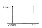
상기 상부 질화 영역(A)과 상기 하부 질화 영역(C) 사이에 존재하고, 질소원자가 미량 또는 거의 존재하지 않는 실리콘 산화막(SiO2)으로 상기 터널 산화막의 절연성 특성을 유지할 수 있다.Exists between the top nitride region (A) and the lower nitride region (C) and nitrogen atoms is possible to maintain the insulating properties of the tunnel oxide film with a very small amount or a silicon oxide film (SiO2) that do not substantially exist.
따라서, 상부 질화 영역(A)및 하부 질화 영역(C)을 포함하는 터널 산화막(110)은 플로팅 게이트와 접하는 상부계면과 실리콘 기판과 접하는 하부 계면에서의 터널 산화막의 신뢰성을 열화시킬 수 있는 손상(Defect), 및 전하 트랩 사이트의 발생을 억제될 수 있어 불 휘발성 메모리 소자의 신뢰성을 개선시킬 수 있다. 또한, 터널 산화막에서 버즈 비크(bird's beak) 생성을 억제할 수 있다.Accordingly, the
박막 처리방법을 이용한 터널 산화막 제조 1Tunnel Oxide Fabrication Using Thin Film Processing Method 1
도 2 내지 도 4는 본 발명의 제1 실시예에 터널 산화막의 제조방법을 나타내는 단면도들이고, 도 5 내지 7은 상기 제1 실시예의 터널 산화막 제조시 산화막의 질소함량 변화를 나타내는 도이다.2 to 4 are cross-sectional views illustrating a method of manufacturing a tunnel oxide film according to the first embodiment of the present invention, and FIGS. 5 to 7 are views illustrating changes in nitrogen content of the oxide film when the tunnel oxide film is manufactured in the first embodiment.
도 2를 참조하면, 기판(100) 상에 산화막(102)을 형성한다. 상기 기판은 실리콘 기판(100)이며, 바람직하게는 소자 분리막(미도시)의 형성으로 액티브 영역과 필드 영역으로 구분된 실리콘 기판(100)이다.Referring to FIG. 2, an
상기 산화막(102)은 실리콘 산화막(SiO2)이다. 상기 실리콘 산화막(102)은 저압 화학 기상 증착(low pressure chemical vapor deposition; LPCVD) 방법으로 실리콘 기판(100) 상에 실리콘 산화물을 증착하여 형성할 수 있다. 상기 실리콘 산화막(102)은 상기 실리콘 기판(100)의 표면을 습식 산화(Wet Oxidation)시켜 형성할 수 있다. 상기 실리콘 산화막(102)은 상기 산소를 포함하는 산화 가스가 제공되는 분위기에서 실리콘 기판(100)의 표면을 열 산화시켜 형성할 수 있다.The
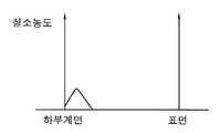
본 실시예의 실리콘 산화막(102)은 산화 가스인 산소 가스(O2)가 제공되는 분위기에서 상기 실리콘 기판의 표면을 열 산화시켜 형성하는 것이 바람직하다. 상기 방법으로 형성된 실리콘 산화막(102)은 도 5에 도시된 그래프와 같이 실리콘 산화막(102)의 표면과 상기 기판과 접하는 산화막의 하부계면에서 질소피크(nitrogen peak)가 관찰되지 않았다.The
도 3을 참조하면, 실리콘 산화막(102)이 형성된 실리콘 기판(100)을 플라즈마 질화(Plasma nitridation)처리하여 표면(top surface)이 질화된 예비 터널 산화막(104)을 형성한다. 여기서, 상기 표면 질화로 인해 상기 실리콘 산화막의 표면아래로 질소가 축적 상부 질화 영역(A)이 형성된다.Referring to FIG. 3, the
상기 예비 터널 산화막(104)은 상부 질화 영역을 포함하고 있기 때문에 도 6에 도시된 그래프와 같이 예비 터널 산화막의 표면에서만 질소피크(nitrogen peak)가 관찰된다. 즉, 상기 예비 터널 산화막의 표면에서만 질소피크가 관찰된다는 것은 상기 질화 플라즈마 처리 공정으로 인해 실리콘 산화막의 표면 특성이 개선되었음을 나타낸다.Since the preliminary
상기 예비 터널 산화막(104)의 형성 방법을 구체적으로 설명한다. 먼저 실리콘 산화막(102)이 형성된 기판(100)을 플라즈마 공정챔버(미도시) 내에 위치시킨다. 이어서, 질소를 포함하는 질화가스를 사용하여 상기 공정챔버 내에서 플라즈마 상태로 여기 시킨다.A method of forming the preliminary
이어서, 질소 라디칼(N*)을 포함하는 질소 플라즈마를 이용하여 실리콘 산화막(102)의 표면을 플라즈마 질화 처리한다. 구체적으로, 상기 플라즈마 질화 처리는 N2 가스, NH3 가스, NO 가스, N2O 가스 등과 같은 질소가스와, Ar 가스와 He 가스 등과 같은 캐리어 가스를 이용하여 약 1mtorr 내지 10torr의 압력 및 상온 내지 약 1000℃의 온도하에서 수행될 수 있다. 그 결과 상기 실리콘 산화막(102)의 표면에 질소가 축적되어 예비 터널 산화막(104)이 형성된다.Subsequently, plasma nitridation is performed on the surface of the
본 실시예의 상기 플라즈마는 공정챔버 내에서 직접 형성하는 방법을 적용하였지만, 별도의 리모트 플라즈마 반응기를 이용하여 상기 질화 가스를 플라즈마 상태로 형성한 후 공정챔버 내부로 플라즈마를 유입시켜 상기 실리콘 산화막의 표면을 플라즈마 질화 처리할 수 있다.In the present embodiment, the plasma is directly formed in the process chamber. However, the nitride gas is formed into a plasma state using a separate remote plasma reactor, and then plasma is introduced into the process chamber to provide a surface of the silicon oxide film. Plasma nitridation treatment.
상기 예비 터널 산화막(104)의 상부 질화 영역(A)은 상기 실리콘 산화막의 상부로 제공된 질소원자가 실리콘 산화막의 실리콘(Si)과 반응하여 Si-N 결합을 갖음으로 형성되고, 그 내부 조직은 치밀한 특성을 갖는다. 따라서 상기 Si-N 결합을 갖는 상부 질화 영역(A)은 플로팅 게이트(미도시)로부터 주입되는 열전자(hot electron)들에 터널 산화막(미도시)이 쉽게 파괴되지 않도록 한다. 또한, 상부 질소 축적 영역(A)은 이후 수소를 포함하는 질화가스가 적용되는 공정을 진행할 경우 상기 터널 산화막(미도시) 내로 수소 침투를 방지한다.The upper nitride region A of the preliminary
도 4를 참조하면, 예비 터널 산화막(104)을 어닐링하여 표면이 질화되고, 기판과 접하는 하부 계면에 질소가 축적된 터널 산화막(110)을 형성한다.Referring to FIG. 4, the preliminary
이하, 터널 산화막(110)의 형성방법을 구체적으로 설명한다. 먼저 예비 터널 산화막(104)이 형성된 기판(100)을 어닐링 공정챔버(미도시) 내로 위치시킨다. 이어서, 질소를 포함하는 질화가스를 사용하여 상기 공정챔버 내에서 상기 예비 터널 산화막(104)을 어닐링 한다. 상기 어닐링에 적용되는 질화가스는 예컨대 N2, NO, N2O, NH3 등을 들 수 있다. 이들은 단독 또는 혼합하여 사용할 수 있다.Hereinafter, a method of forming the
상기 어닐링은 상기 플라즈마 질화 처리 공정이 수행된 공정 챔버에서 인시튜(in-situ)로 수행할 수 있다. 상기 어닐링은 일 예로 800 내지 1100℃의 온도에서 상기 실리콘 기판을 수 십초 동안 급속 열처리 공정(RTP)을 수행하여 형성할 수 있다. 또한, 상기 어닐링은 500 내지 1200℃의 온도를 갖는 퍼니스에서 수 내지 수십 시간 동안 열 처리하여 형성할 수 있다.The annealing may be performed in-situ in a process chamber in which the plasma nitridation process is performed. For example, the annealing may be formed by performing a rapid heat treatment (RTP) process on the silicon substrate for several tens of seconds at a temperature of 800 to 1100 ° C. In addition, the annealing may be formed by heat treatment for several to several tens of hours in a furnace having a temperature of 500 to 1200 ℃.
상기 어닐링은 플라즈마 질화 처리 공정시 초래되는 상기 실리콘 산화막의 손상(damege)을 큐어링하여 터널 산화막(110) 내부에서의 전하 트랩 사이트 생성을 억제한다. 또한, 상기 어닐링은 터널 산화막(110)내에서 실리콘과 산소의 댕글링 결합(dangling bonds), 실리콘과 산소 결합의 스트레인(Strain), 실리콘과 산소 결합의 스트레치(Stretch)를 치유하여 터널 산화막의 특성 및 신뢰성을 향상시킨다.The annealing cures damage of the silicon oxide film caused during the plasma nitridation process, thereby suppressing charge trap site generation in the
또한, 어닐링 공정은 열에 의해 분해되어 형성된 질소 원자를 상기 기판과 접하는 예비 터널 산화막(104)의 하부 계면으로 확산 침투시키는 동시에 상기 예비 터널 산화막(104)의 상부 질화 영역(A)역에 포함된 질소원자를 상기 실리콘 산화막의 하부 계면으로 열 확산시킬 수 있다. 열 확산된 질소원자는 상기 예비 터널 산화막(104)의 하부 계면에 축적됨으로서 상기 예비 터널 산화막은 터널 산화막(110)으로 형성된다.In addition, the annealing process diffuses and infiltrates nitrogen atoms formed by decomposition by heat into the lower interface of the preliminary
상기 예비 터널 산화막의 어닐링으로 터널 산화막에는 하부 질화 영역이 형성되므로 인해 상기 터널 산화막은 도 7에 도시된 그래프와 같이 산화막 표면 및 기판과 접하는 산화막 하부계면 각각에서 질소 피크(nitrogen peak)가 관찰되었다. 즉, 상기 터널 산화막의 표면과 하부 계면은 질화되어 그 특성이 모두 개선될 수 있음을 나타낸다.Since the lower nitride region is formed in the tunnel oxide layer by the annealing of the preliminary tunnel oxide layer, a nitrogen peak was observed in each of the tunnel oxide layer on the oxide layer surface and the oxide layer interface in contact with the substrate as shown in FIG. 7. That is, the surface and the lower interface of the tunnel oxide film are nitrided, indicating that all of its characteristics can be improved.
상기한 방법으로 형성되어 표면과 하부 계면이 모두 질화된 터널 산화막은 이후 증착 공정 또는 열처리 공정을 수행할 경우 터널 산화막 내로 수소가 침투되는 것을 방지할 수 있다. 또한, 그 내부에서의 전하 트랩 사이트의 생성을 방지함으로서 불 휘발성 메모리 셀의 누설전류를 감소 및 신뢰성을 증가시킬 수 있다.The tunnel oxide film formed by the above-described method and nitrided on both the surface and the lower interface may prevent hydrogen from penetrating into the tunnel oxide film when the deposition process or the heat treatment process is performed. In addition, by preventing generation of charge trap sites therein, it is possible to reduce leakage current and increase reliability of nonvolatile memory cells.
박막 처리방법을 이용한 터널 산화막 제조 2Tunnel Oxide Fabrication Using Thin Film Processing Method 2
도 8 내지 도 11은 본 발명의 제2 실시예에 따른 터널 산화막의 제조방법을 나타내는 단면도들이고, 도 12 내지 15는 상기 제2 실시예의 터널 산화막 제조시 질소함량의 변화를 나타내는 도이다.8 to 11 are cross-sectional views illustrating a method of manufacturing a tunnel oxide film according to a second embodiment of the present invention, and FIGS. 12 to 15 illustrate changes in nitrogen content when the tunnel oxide film is manufactured in the second embodiment.
도 8을 참조하면, 기판(200) 상에 산화막(202)을 형성한다. 상기 기판은 실리콘 기판(200)이며, 바람직하게는 소자 분리막(미도시)의 형성으로 액티브 영역과 필드 영역으로 구분된 실리콘 기판(200)이다.Referring to FIG. 8, an
상기 산화막(202)은 실리콘 산화막(SiO2)으로 저압 화학 기상 증착(low pressure chemical vapor deposition; LPCVD) 방법, 습식 산화(Wet Oxidation)방법 및 열 산화방법으로 형성할 수 있다. 상기 실리콘 산화막(202)은 산화가스인 오존 가스(O3)가 제공되는 분위기에서 상기 실리콘 기판의 표면을 열 산화시켜 형성하는 것이 바람직하다.The
열 산화 방법으로 형성된 실리콘 산화막(202)은 도 12에 도시된 그래프와 같이 실리콘 산화막(202)의 표면과 하부계면에서 질소피크(nitrogen peak)가 관찰되지 않았다. 상기 질소피크가 관찰되지 않는다는 것은 상기 실리콘 산화막의 표면과 하부 계면에 질소를 포함되어 있지 않음을 나타낸다.In the
도 9를 참조하면, 실리콘 산화막(202)이 형성된 실리콘 기판(200)을 열 질화(thermal nitridation)처리하여 기판과 접하는 실리콘 산화막의 하부 계면(bottom surface)에 질소(N)가 축적된 제1 예비 터널 산화막(204)을 형성한다. 또한, 다른 실시예로 열 질화처리 공정은 실리콘 산화막을 플라즈마 질화 처리한 이후 수행할 수도 있다.Referring to FIG. 9, a first preliminary structure in which nitrogen (N) is accumulated on a bottom surface of a silicon oxide film contacting the substrate by thermal nitridation of the
여기서, 질소가 축적된 실리콘 산화막의 하부 계면을 하부 질화 영역(C)이라 한다. 상기 제1 예비 터널 산화막(204)은 하부 질화 영역(C)을 포함하고 있다. 도 13을 참조하면, 제1 예비 터널 산화막은 하부 계면에서만 질소피크(nitrogen peak)가 관찰되었다. 상기 제1 예비 터널 산화막(204)의 하부 계면에서만 질소피크가 관찰된다는 것은 상기 열 플라즈마 처리 공정으로 인해 실리콘 산화막의 하부 계면 특성이 개선되었음을 나타낸다. Here, the lower interface of the silicon oxide film in which nitrogen is accumulated is referred to as the lower nitride region (C). The first preliminary
이하. 제1 예비 터널 산화막(204)의 형성 방법을 구체적으로 설명한다. 먼저 실리콘 산화막(202)이 형성된 기판(100)을 공정챔버(미도시) 내에 위치시킨다. 이어서, 질소를 포함하는 질화가스를 공정챔버 내로 제공하여 상기 질화가스를 열분해 시킨다. 상기 질소를 포함하는 질화가스는 예컨대 N2, NO, N2O, NH3 등을 들 수 있다. 이들은 단독 또는 혼합하여 사용할 수 있다.Below. A method of forming the first preliminary
이어서, 상기 공정챔버 내에서 열 분해되어 형성된 질소 원자를 적용하여 상기 실리콘 산화막을 질화 처리한다. 그 결과 열 분해된 질소 원자는 상기 실리콘 산화막의 표면로부터 하부 계면으로 확산되어 상기 실리콘 산화막의 하부 계면에 축적된다. 이로 인해 상기 실리콘 산화막은 제1 예비 터널 산화막으로 형성된다.Subsequently, the silicon oxide film is nitrided by applying nitrogen atoms formed by thermal decomposition in the process chamber. As a result, the thermally decomposed nitrogen atoms diffuse from the surface of the silicon oxide film to the lower interface and accumulate at the lower interface of the silicon oxide film. As a result, the silicon oxide film is formed as a first preliminary tunnel oxide film.
도 10을 참조하면, 제1 예비 터널 산화막(204)이 형성된 실리콘 기판(200)을 플라즈마 질화(Plasma nitridation)처리하여 그 표면(top surface)이 질화된 제2 예비 터널 산화막(206)을 형성한다.Referring to FIG. 10, the
다른 실시예로 상기 플라즈마 질화처리 공정은 상기 실리콘 산화막 형성한 후 수행할 수 있다.In another embodiment, the plasma nitridation process may be performed after the silicon oxide film is formed.
상기 플라즈마 질화 처리공정은 상기 제1 예비 터널 산화막(204)의 표면에 질소 원자를 축적시키는 공정으로 상부 질화 영역(A)을 갖는 제2 예비 터널 산화막(206)을 형성한다.The plasma nitridation process is a process of accumulating nitrogen atoms on the surface of the first preliminary
상기 제2 예비 터널 산화막(206)은 상부 질화 영역(A)을 포함하고 있어 도 14에 도시된 그래프와 같이 제2 예비 터널 산화막의 표면 하부계면에서 질소피크(nitrogen peak)가 관찰되었다.The second preliminary
즉, 상기 제2 예비 터널 산화막의 표면에서 질소피크가 관찰되는 것은 상기 질화 플라즈마 처리 공정으로 인해 실리콘 산화막의 표면의 특성이 개선될 수 있음을 나타낸다.That is, the observation of nitrogen peak on the surface of the second preliminary tunnel oxide film indicates that the characteristics of the surface of the silicon oxide film may be improved by the nitride plasma treatment process.
상기 플라즈마 질화 처리 공정을 수행하여 제1 예비 터널 산화막의 표면을 질화시키는 공정에 대한 구체적인 설명은 상기 도 3의 설명에서 상세히 설명하였기 때문에 중복을 피하기 위해 생략하기로 한다.A detailed description of the process of nitriding the surface of the first preliminary tunnel oxide layer by performing the plasma nitriding process is described in detail with reference to FIG. 3, and thus, description thereof will be omitted to avoid duplication.
질화 플라즈마 처리 공정으로 형성된 상기 제2 예비 터널 산화막(206)의 상부 질화영역(A)은 상기 제1 예비 터널 산화막의 상부로 제공된 질소 라디칼이 실리콘 산화막의 실리콘(Si)과 반응하여 Si-N 결합을 갖음으로서 형성된 영역이다. 따라서 상기 Si-N 결합을 갖는 상부 질화 영역(A)은 플로팅 게이트(미도시)로부터 주입되는 열 전자(hot electron)들에 터널 산화막(미도시)이 쉽게 파괴되지 않도록 한다. 또한, 상부 질화영역(A)은 이후 수소를 포함하는 질화가스가 적용되는 공정을 진행할 경우 터널 산화막(미도시) 내로 수소 침투를 방지한다.In the upper nitride region A of the second preliminary
도 11을 참조하면, 제2 예비 터널 산화막(206)을 어닐링하여 내부의 결함이 치유된 터널 산화막(210)을 형성한다.Referring to FIG. 11, the second preliminary
이하, 터널 산화막(210)의 형성 방법을 구체적으로 설명한다. 먼저 제2 예비 터널 산화막(206)이 형성된 기판(200)을 어닐링을 수행하기 위한 챔버(미도시) 내로 위치시킨다. 이어서, 질소를 포함하는 질화가스를 사용하여 상기 챔버 내에서 상기 제2 예비 터널 산화막(206)을 어닐링 한다. 상기 어닐링에 적용되는 가스로는 예컨대 Ar, N2, NO, N2O, NH3 등을 들 수 있다. 이들은 단독 또는 혼합하여 사용할 수 있다.Hereinafter, a method of forming the
상기 어닐링은 플라즈마 질화처리 공정시 제2 예비 터널 산화막의 내부 결함을 충분히 치유하기 위하여 열이 제공되는 분위기에서 수초 내지 수 시간 동안 수행된다. 일 예로서, 급속 열처리(rapid thermal process; RTP) 장치를 이용하여 상기 어닐링을 수행할 경우, 상기 어닐링은 수초 내지 수 십초 동안 수행될 수 있으며, 퍼니스(furnace) 타입의 어릴닝 장치를 사용하는 경우, 상기 어닐링은 수분 내지 수 시간 동안 수행될 수 있다. 상기 결함은 예컨대 상기 플라즈마 질화처리 공정시 생성된 전하 트랩 사이트, 실리콘과 산소의 댕글링 결합(dangling bonds), 실리콘과 산소 결합의 스트레인(Strain), 실리콘과 산소 결합의 스트레치(Stretch)등을 들 수 있다.The annealing is performed for several seconds to several hours in an atmosphere provided with heat to sufficiently heal internal defects of the second preliminary tunnel oxide film during the plasma nitridation process. As an example, when the annealing is performed using a rapid thermal process (RTP) apparatus, the annealing may be performed for several seconds to several tens of seconds, and when an furnace-type annealing apparatus is used. The annealing may be performed for several minutes to several hours. The defects include, for example, charge trap sites generated during the plasma nitridation process, dangling bonds of silicon and oxygen, strains of silicon and oxygen bonds, stretches of silicon and oxygen bonds, and the like. Can be.
상기 어닐링 공정은 어닐링 공정시 열에 의해 분해되어 형성된 질소 원자를 상기 예비 터널 산화막(204)의 하부 계면으로 확산 침투시키는 동시에 상기 제2 예비 터널 산화막(206)의 상부 질화 영역(A)역에 포함된 질소원자를 상기 실리콘 산화막의 하부 계면으로 확산시킬 수 있다. In the annealing process, nitrogen atoms decomposed by heat during the annealing process diffuse and penetrate into the lower interface of the preliminary
상기 어닐링 공정을 수행하여 완성된 터널 산화막(210)은 전하 트랩 사이트, 실리콘과 산소의 댕글링 결합(dangling bonds), 실리콘과 산소 결합의 스트레인(Strain), 실리콘과 산소 결합의 스트레치(Stretch)등이 발생하는 문제점이 감소되었다. 도 15를 참조하면, 상기 터널 산화막(210)은 상부계면 및 하부계면에서 질소 피크(nitrogen peak)가 관찰되었다. 특히, 도 15에서의 터널 산화막 상부 계면의 질소 피크는 도 14에서 관찰된 예비 터널 산화막 상부 계면의 질소 피크보다 더 넓게 분포하는 것을 확인할 수 있었다. 이것은 어닐링의 열 처리에 의해 상기 상부 계면에 축적된 질소 원자가 상기 하부계면으로 이동하였기 때문이다.The
상기한 방법으로 형성되어 표면과 하부 계면이 모두 질화된 터널 산화막은 이후 증착 공정 또는 열처리 공정을 수행할 경우 터널 산화막 내로 수소가 침투되는 것을 방지할 수 있다. 또한, 그 내부에서의 전하 트랩 사이트의 생성을 방지함으로서 불 휘발성 메모리 셀의 누설전류를 감소 및 신뢰성을 증가시킬 수 있다.The tunnel oxide film formed by the above-described method and nitrided on both the surface and the lower interface may prevent hydrogen from penetrating into the tunnel oxide film when the deposition process or the heat treatment process is performed. In addition, by preventing generation of charge trap sites therein, it is possible to reduce leakage current and increase reliability of nonvolatile memory cells.
불 휘발성 메모리 셀 제조 1Nonvolatile Memory Cell Manufacturing 1
도 16 내지 도 22는 본 발명의 제1 실시예에 따른 불 휘발성 메모리 셀의 형성방법을 나타내는 단면도들이다. 여기서, 상기 도 16 내지 21은 불 휘발성 메모리 셀의 워드라인 방향의 단면도이고, 도 22는 불 휘발성 메모리 셀의 비트라인 방향의 단면도이다.16 to 22 are cross-sectional views illustrating a method of forming a nonvolatile memory cell in accordance with a first embodiment of the present invention. 16 to 21 are cross-sectional views in a word line direction of a nonvolatile memory cell, and FIG. 22 is a cross-sectional view in a bit line direction of a nonvolatile memory cell.
도 16에 도시된 바와 같이, 기판(100)상에 터널 산화막(110), 제1 도전막(114) 및 제1 마스크 패턴(M1)을 순차적으로 형성한다.As shown in FIG. 16, the
먼저 실리콘으로 이루어진 기판(100)상에 표면(Top surface)과 하부 계면(bottom interface)에 질소원자가 축적되고, 내부 결함이 치유된 터널 산화막(110)을 형성한다.First, nitrogen atoms are accumulated on a top surface and a bottom interface on a
불 휘발성 반도체 메모리 장치에 있어서, 저장된 데이터를 보존하는 능력은 대체로 터널 산화막(110)의 신뢰성에 의존되기 때문에 터널 산화막(110)은 프로그래밍 동작과 소거 동작을 반복하는 횟수에 제한적인 요소로 작용한다. 통상적인 불 휘발성 반도체 메모리 장치는 적어도 약 100만회 이상의 프로그래밍 동작과 소거 동작을 반복할 수 있는 것이 요구된다. 이에 따라 본 발명의 터널 산화막은 제1 실시예 방법과 제2 실시예 방법으로 형성되어 표면이 질화되고, 하부 계면에 질소원자가 축적된 것이 바람직하다.In the nonvolatile semiconductor memory device, the ability to preserve the stored data is largely dependent on the reliability of the
제1 실시예에 따른 터널 산화막(110)막 형성방법에 있어서, 먼저 액티브 영역에 해당하는 실리콘 기판에 실리콘 산화막(미도시)을 형성한 후 상기 실리콘 산화막을 질소가스가 제공되는 분위기에서 플라즈마 질화 처리하여 상기 산화막의 표면을 질화시킨다. 상기 플라즈마 질화 처리로 인해 상기 질소원자는 실리콘 산화막의 표면 아래로 축적되어 상부 질화 영역이 형성된다. 이어서, 상부 질화 영역이 형성된 실리콘 산화막을 어닐링(annealing)하여 상기 플라즈마 질화처리 공정시 발 생된 실리콘 산화막 내의 결함을 큐어링하는 동시에 상기 산화막의 하부 계면에 질소를 축적시켜 터널 산화막을 형성할 수 있다. 상기 제1 실시예에 따른 터널 산화막의 형성방법에 대한 구체적인 설명은 도 2 내지 도 4의 상세한 설명에 기재되어 있어 중복된 설명은 생략한다.In the method for forming a
또한, 제2 실시예에 따른 터널 산화막(110)을 형성방법에 있어서, 먼저 액티브 영역에 해당하는 실리콘 기판의 표면에 실리콘 산화막을 형성한 후 상기 실리콘 산화막을 질소가스가 제공되는 분위기에서 열 질화 처리하여 상기 기판가 접하는 실리콘 산화막의 하부 계면을 질화시킨다. 이어서, 질소가스가 제공되는 분위기에서 상기 실리콘 산화막을 플라즈마 질화 처리하여 상기 산화막의 표면을 질화 처리한다. 상기 플라즈마 질화 처리로 인해 상기 질소원자가 실리콘 산화막의 표면 아래에 축적되어 상부 질화영역이 형성된다. 이어서, 상부 질화영역이 형성된 실리콘 산화막을 어닐링(annealing)하여 상기 플라즈마 질화처리 공정시 발생된 실리콘 산화막 내의 결함을 큐어링하여 신뢰성이 우수한 터널 산화막을 형성할 수 있다. 상기 제2 방법으로 터널 산화막을 형성하기 위한 구체적인 설명은 도 2 내지 도 4의 상세한 설명에 기재되어 있어 중복된 설명은 생략한다.In the method of forming the
상기한 제1 실시예 및 제2 실시예 방법으로 형성되어 상부 계면과 하부 계면에 질소가 축적된 터널 산화막은 이후 증착 공정 또는 열처리 공정을 수행할 경우 터널 산화막 내로 수소가 침투되는 것을 방지할 수 있고, 그 내부에서의 전하 트랩 사이트의 생성 방지 및 터널 산화막과 실리콘 기판 사이의 계면 균일도가 향상되는 특성을 갖는다.The tunnel oxide film formed by the method of the first and second embodiments described above and accumulated nitrogen at the upper and lower interfaces may prevent hydrogen from penetrating into the tunnel oxide film when the deposition process or the heat treatment process is performed. This has the characteristics of preventing generation of charge trap sites therein and improving the uniformity of the interface between the tunnel oxide film and the silicon substrate.
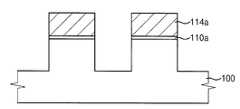
이어서, 터널 산화막(110) 상에 플로팅 게이트용 제1 도전막(114)을 형성한다. 상기 제1 도전막(114)은 저압 화학 기상 증착(low pressure chemical vapor deposition; LPCVD)하여 약 500Å의 두께로 형성한 후, 통상의 도핑 방법인 POCl3 확산, 이온주입, 또는 인-시튜 도핑 방법으로 불순물로 도핑함으로서 형성할 수 있다. 여기서, 제1 도전막(114)은 폴리실리콘 또는 비정질실리콘으로 형성하는 것이 바람직하다. 이어서, 제1 도전막(114)상에 플로팅 게이트의 레이아웃(형성 영역)을 정의하는 마스크 패턴(M1)을 형성한다.Subsequently, a floating conductive first
상기 제1 마스크 패턴(M1)은 마스크층(미도시) 및 포토레지스트 패턴(미도시)을 형성한 후 상기 포토레지스트 패턴에 노출된 마스크층을 식각함으로서 형성된다. 상기 마스크층은 실리콘 질화물로 이루어질 수 있으며, SiH2Cl2 가스, SiH4 가스, NH3 가스 등을 이용하는 저압 화학 기상 증착(Low Pressure Chemical Vapor Deposition; LPCVD) 공정 또는 플라즈마 강화 화학 기상 증착(plasma enhanced chemical vapor deposition; PECVD) 공정을 통해 형성될 수 있다. 상기 포토레지스트 패턴은 제1 마스크 패턴(M1)을 형성한 후 애싱 공정(ashing process) 및 세정 공정을 수행하여 상기 포토레지스트 패턴은 제거된다.The first mask pattern M1 is formed by forming a mask layer (not shown) and a photoresist pattern (not shown) and then etching the mask layer exposed to the photoresist pattern. The mask layer may be formed of silicon nitride, and may be a low pressure chemical vapor deposition (LPCVD) process or a plasma enhanced chemical vapor deposition process using SiH2 Cl2 gas, SiH4 gas, NH3 gas, or the like. It may be formed through a chemical vapor deposition (PECVD) process. After forming the first mask pattern M1, the photoresist pattern may be subjected to an ashing process and a cleaning process to remove the photoresist pattern.
도 17에 도시된 바와 같이, 제1 도전막 패턴(114a) 사이에 정렬된 트렌치를 포함하는 실리콘 기판(100)을 형성한다.As illustrated in FIG. 17, a
이를 구체적으로 설명하면, 상기 제1 마스크 패턴(M1)에 노출된 제1 도전막(114)과 터널 산화막(102) 및 실리콘 기판(100)의 상부를 식각하기 위해 실리콘 기 판(100)을 식각 챔버 내로 이송한다. 이후, 제1 도전막(114) 및 터널 산화막(110)을 식각하기 위한 에칭 가스를 상기 식각 챔버 내로 주입하여, 상기 제1 마스크 패턴(M1)에 노출된 제1 도전막(114) 및 터널 산화막(110)을 순차적으로 식각한다. 상기 식각 공정으로 제1 도전막(114)은 제1 도전막 패턴(114a)으로, 터널 산화막(110)은 터널 산화막 패턴(110a)으로 형성된다.In detail, the
이어서, 동일한 식각 챔버 내에서 상기 실리콘 기판(100)을 약 1200 내지 2500Å 정도의 깊이, 바람직하게는 1700Å의 깊이로 식각하여 상기 실리콘 기판에 제1 방향으로 연장된 트렌치(미도시)를 형성한다. 즉, 상기 트렌치의 형성에 인해 상기 실리콘 기판은 액티브 영역과 플로팅 게이트 형성 영역이 동시에 정의된다.Subsequently, in the same etching chamber, the
일 예로 상기 트렌치를 형성하기 위한 식각 공정시 야기된 실리콘 기판의 손상을 치유하고, 누설 전류 발생을 방지하기 위해 상기 트렌치의 내 측면에 라이너막을 더 형성할 수 있다.For example, a liner layer may be further formed on an inner side surface of the trench to cure damage to the silicon substrate caused by an etching process for forming the trench and to prevent leakage current.
도 18 도시된 바와 같이, 산화물 증착공정 및 화학적 기계적 연마공정을 수행하여 기판의 트렌치내에 소자 분리막(112)을 형성한다. 먼저, 상기 트렌치를 매립하기 위해 갭 필링 특성이 우수한 절연물을 화학적 기상증착 방법으로 증착한다. 이때, 상기 산화물은 고밀도 플라즈마(HDP) 산화물인 것이 바람직하다. 이후, 상기 제1 마스크 패턴의 표면이 노출되도록 상기 산화물에 화학적 기계적 연마공정(CMP)을 수행하여, 트렌치에 존재하는 소자분리막(112)을 형성한다. 이후 상기 제1 마스크 패턴을 제거한다.As shown in FIG. 18, an oxide deposition process and a chemical mechanical polishing process are performed to form the
도 19에 도시된 바와 같이, 상기 제1 도전막 패턴(114a) 상에 제2 도전막 패 턴(116a)을 형성하여 예비 플로팅 게이트(120)를 형성한다.As illustrated in FIG. 19, a second
먼저, 상기 제1 도전막 패턴(114a)이 노출된 결과물 상에 플로팅 게이트용 제2 도전막(도시하지 않음)을 저압 화학 기상 증착(low pressure chemical vapor deposition; LPCVD) 방법으로 형성한다. 상기 제2 도전막은 도핑된 폴리실리콘 또는 금속 물질을 증착하여 형성할 수 있다. 즉, 제2 도전막은 N+형으로 도핑된 폴리 실리콘막으로 구성되거나 또는 폴리실리콘막으로 이루어진다.First, a second conductive film (not shown) for a floating gate is formed on a resultant product to which the first
이후, 제2 도전막 상에 플로팅 게이트(120)의 레이아웃을 정의하는 식각 마스크(미도시)를 형성한다. 이어서, 상기 식각 마스크에 노출된 상기 제2 도전막을 건식 식각하여 제2 도전막 패턴(116a)을 형성한다. 이후 상기 식각 마스크를 제거한다. 여기서, 상기 예비 플로팅 게이트(120)는 제1 도전막 패턴(114a)과 제2 도전 막 패턴(116a)이 적층되어 형성된다.Thereafter, an etching mask (not shown) defining a layout of the floating
도 20을 참조하면, 상기 예비 플로팅 게이트(120)형성된 기판 상에 유전막(130)을 형성한다.Referring to FIG. 20, a
상기 유전막(130)은 실리콘 산화막/실리콘 질화막/실리콘 산화막을 순차적으로 적층하여 형성할 수 있다. 다른 실시예로 상기 유전막(130)은 고유전율을 갖는 금속 산화물을 증착하여 형성할 수 있다.The
상기 유전막(130)을 형성할 수 있는 금속산화물의 예로서 HfO2, ZrO2, Ta2O5, Y2O3, Nb2O5, Al2O3, TiO2, CeO2, In2O3, RuO2, MgO, SrO, B2O3, SnO2, PbO, PbO2, Pb3O4, V2O3, La2O3, Pr2O3, Sb2O3, Sb2O5, CaO 등을 들 수 있다. 이들은 단독으로 사용하는 것이 바람직하고, 경우에 따라서 둘 이상을 사용할 수도 있다.Examples of the metal oxide capable of forming the
예를 들어, 상기 유전막(130)은 실리콘 산화막, 실리콘 질화막 및 고유전율을 갖는 금속 산화막을 순차적으로 적층하여 형성할 수 있고, 금속 산화막, 실리콘 질화막, 금속 산화막을 순차적으로 적층하여 형성할 수 있다. 예컨대 상기 금속산화막은 금속 전구체를 이용한 원자층 증착방법 또는 화학적 기상 증착 방법으로 형성할 수 있다.For example, the
도 21을 참조하면, 상기 유전막(130) 상에 예비 컨트롤 게이트(140)를 형성한다. 상기 예비 컨트롤 게이트는 도핑된 폴리실리콘 또는 금속 물질을 증착하여 형성할 수 있다. 즉, 예비 컨트롤 게이트는 N+형으로 도핑된 폴리 실리콘막으로 이루어지거나 폴리실리콘막 및 금속 실리사이드막으로 이루어지거나, 폴리실리콘막 및 금속막으로 금속막으로 이루어진다. 이 경우, 상기 금속 실리사이드은 텅스텐 실리사이드(WSiX), 티타늄 실리사이드(TiSiX), 코발트 실리사이드(CoSiX), 또는 탄탈륨 실리사이드(TaSiX) 등을 포함한다. 상기 금속은 텅스텐, 티타늄 등을 포함한다.Referring to FIG. 21, a
이어서, 상기 예비 컨트롤 게이트(140) 상에 게이트 구조물의 형성영역을 정의하는 제2 마스크 패턴(미도시)을 형성한다. 상기 제2 마스크 패턴의 형성하기 위해서는 먼저, SiH2Cl2 가스, SiH4 가스, NH3 가스등을 이용하는 저압 화학 기상 증착(Low Pressure Chemical Vapor Deposition; LPCVD) 공정 또는 플라즈마 강화 화학 기상 증착(plasma enhanced chemical vapor deposition; PECVD) 공정을 수행 하여 실리콘 질화막을 형성한다.Subsequently, a second mask pattern (not shown) defining a region in which a gate structure is formed is formed on the
이어서, 상기 실리콘 질화막 상에 포토리소그래피(photolithography) 공정을 수행함으로서 형성된 포토레지스트 패턴(미도시)을 형성한다. 이어서, 상기 포토레지스트 패턴에 노출된 실리콘 질화막을 패터닝한다. 그 결과 제2 마스크 패턴(미도시)이 형성된다. 상기 제2 마스크 패턴은 제1 방향으로 연장된 소자 분리막(112)과 수직하는 제2 방향으로 연장되는 라인 형상을 갖는다.Subsequently, a photoresist pattern (not shown) formed by performing a photolithography process is formed on the silicon nitride film. Subsequently, the silicon nitride film exposed to the photoresist pattern is patterned. As a result, a second mask pattern (not shown) is formed. The second mask pattern has a line shape extending in a second direction perpendicular to the
이후, 상기 제2 마스크 패턴을 형성한 후 애싱 공정(ashing process) 및 세정 공정을 수행하여 상기 포토레지스트 패턴을 제거한다.Thereafter, after forming the second mask pattern, an ashing process and a cleaning process are performed to remove the photoresist pattern.
도 22를 참조하면, 상기 제2 마스크 패턴에 노출된 상기 예비 컨트롤 게이트(140), 유전막(130) 및 상기 예비 플로팅 게이트(120)를 순차적으로 식각하여 불 휘발성 메모리 셀의 게이트 구조물(150)을 형성한다. 상기 게이트 구조물은 터널 산화막 패턴(110a)상에 플로팅 게이트(120a), 유전막 패턴(130a) 및 컨트롤 게이트(140a)가 순차적으로 적층된 구조를 갖는다.Referring to FIG. 22, the
불 휘발성 메모리 셀 제조 2Nonvolatile Memory Cell Manufacturing 2
도 23 내지 도 27은 본 발명의 제2 실시예에 따른 불 휘발성 메모리 셀의 형성방법을 나타내는 단면도들이다. 여기서, 상기 도 23 내지 26은 불 휘발성 메모리 셀의 워드라인 방향의 단면도이고, 도 27은 불 휘발성 메모리 셀의 비트라인 방향의 단면도이다.23 to 27 are cross-sectional views illustrating a method of forming a nonvolatile memory cell in accordance with a second embodiment of the present invention. 23 to 26 are cross-sectional views of a nonvolatile memory cell in a word line direction, and FIG. 27 is a cross-sectional view of a nonvolatile memory cell in a bit line direction.
도 23을 참조하면, 소자 분리 공정을 수행하여 예비 소자 분리막이 형성된 실리콘 기판을 형성한다.Referring to FIG. 23, a silicon substrate on which a preliminary device isolation layer is formed is formed by performing a device isolation process.
상기 예비 소자분리막이 형성된 실리콘 기판의 형성방법을 구체적으로 설명하면, 먼저, 실리콘 기판(200) 상에 패드 산화막(미도시)을 형성하고, 상기 패드 산화막 상에 하드 마스크층을 형성한다. 상기 패드 산화막은 열산화(thermal oxidation) 공정, 화학 기상 증착(chemical vapor deposition; CVD) 공정 등을 통해 형성될 수 있다. 상기 마스크층은 실리콘 질화물을 저압 화학 기상 증착(Low Pressure Chemical Vapor Deposition; LPCVD) 공정 또는 플라즈마 강화 화학 기상 증착(plasma enhanced chemical vapor deposition; PECVD) 공정을 수행하여 형성할 수 있다.A method of forming the silicon substrate on which the preliminary device isolation layer is formed will be described in detail. First, a pad oxide film (not shown) is formed on the
이어서, 상기 마스크층 상에 포토레지스트 패턴(미도시)을 형성한 후 포토레지스트 패턴에 노출된 마스크층을 식각하여 마스크 패턴(미도시)을 형성한다. 이후, 상기 포토레지스트 패턴은 마스크 패턴을 형성한 후 애싱 공정(ashing process) 및 세정 공정을 수행하여 제거된다.Subsequently, after forming a photoresist pattern (not shown) on the mask layer, the mask layer exposed to the photoresist pattern is etched to form a mask pattern (not shown). Thereafter, the photoresist pattern is removed by forming an mask pattern and then performing an ashing process and a cleaning process.
이어서, 상기 마스크 패턴을 식각 마스크로 적용하여 상기 패드 산화막 및 실리콘 기판의 상부를 식각함으로써 실리콘 기판에 제1 방향으로 연장되는 트렌치(미도시)를 형성한다. 상기 트렌치는 약 1000Å 내지 5000Å 정도의 깊이를 갖도록 형성할 수 있고, 특히 약 2300Å 정도의 깊이를 갖도록 형성할 수 있다.Subsequently, the mask pattern is applied as an etching mask to etch upper portions of the pad oxide layer and the silicon substrate to form trenches (not shown) extending in the first direction in the silicon substrate. The trench may be formed to have a depth of about 1000 kPa to 5000 kPa, and in particular, may be formed to have a depth of about 2300 kPa.
이어서, 상기 트렌치를 형성하기 위한 식각공정시 생성되는 실리콘 기판의 손상을 치유하고, 누설 전류 발생을 방지하기 위해 상기 트렌치의 내 측면에 라이너막을 더 형성할 수 있다.Subsequently, a liner layer may be further formed on an inner side surface of the trench to cure damage to the silicon substrate generated during the etching process for forming the trench and to prevent leakage current.
이어서, 상기 트렌치가 형성된 실리콘 기판 상에 소자분리용 절연물(미도시)을 층착하여 상기 트렌치를 매몰한다. 이어서, 상기 실리콘 기판에 증착된 소자분용 절연물의 상기 마스크 패턴의 상면에 노출될 때까지 평탄화 공정을 수행하여 예비 소자 분리막(212)을 형성한다. 상기 평탄화 공정으로 화학적 기계적 연마(chemical mechanical polishing; CMP) 공정을 적용할 수 있다.Subsequently, an insulator (not shown) for device isolation is deposited on the silicon substrate on which the trench is formed to bury the trench. Subsequently, the preliminary
상기 예비 소자 분리막(212)의 형성으로 상기 실리콘 기판(200)은 액티브 영역과 소자분리 영역으로 정의된다. 이어서, 상기 마스크 패턴 및 패드 산화막을 제거하여 기판의 상면이 노출시킨다.The
이어서, 상기 액티브 영역에 해당하는 실리콘 기판(200)의 상에 표면 및 하부 계면에 질소원자가 축적되고, 내부 결함이 치유된 터널 산화막(210)을 형성한다. 본 발명의 터널 산화막(210)은 제1 실시예 방법과 제2 실시예 방법으로 형성되어 상부 계면과 하부 계면에 질소원자가 축적되어 있는 것이 바람직하다.Subsequently, nitrogen atoms are accumulated on the surface and the lower interface on the
상기 제1 실시예에 따른 터널 산화막의 형성방법에 대한 구체적인 설명은 도 2 내지 도 4의 상세한 설명에 기재되어 있고, 상기 제2 방법으로 터널 산화막을 형성하기 위한 구체적인 설명은 도 2 내지 도 4의 상세한 설명에 기재되어 있어 중복된 내용은 생략하였다.A detailed description of the method for forming the tunnel oxide film according to the first embodiment is described in the detailed description of FIGS. 2 to 4, and the detailed description for forming the tunnel oxide film by the second method is described with reference to FIGS. 2 to 4. Duplicate content is omitted since it is described in the detailed description.
상기한 제1 실시예 및 제2 실시예 방법으로 형성되어 상부 계면과 하부 계면에 질소가 축적된 터널 산화막(210)은 후속 공정을 수행할 경우 터널 산화막 내로 수소가 침투되는 것을 방지할 수 있고, 그 내부에서의 전하 트랩 사이트의 생성 방지 및 터널 산화막과 실리콘 기판 사이의 계면 균일도가 향상되는 특성을 갖는다.The
도 24를 참조하면, 상기 예비 소자 분리막(212) 사이의 트렌치를 완전히 매립하면서 상기 예비 소자 분리막(212) 상에 플로팅 게이트용 제1 도전막(도시안됨)을 형성한다. 이어서, 화학 기계적 연마 공정을 수행하여 상기 예비 소자 분리막 패턴(212)의 상부면이 노출되도록 상기 제1 도전막을 평탄화시킴으로서, 예비 플로팅 게이트(220)를 형성한다.Referring to FIG. 24, a first conductive film for a floating gate (not shown) is formed on the preliminary
도 25를 참조하면, 상기 예비 플로팅 게이트(220)의 상부 측벽이 일부 노출되도록 상기 예비 소자 분리막(212)을 상부를 식각함으로서 소자 분리막(212a)을 완성한다. 이 때, 상기 소자 분리막(212a)은 상기 액티브 영역의 실리콘 기판 상부면 보다는 높게 위치하는 것이 바람직하다.Referring to FIG. 25, the
이어서, 상기 예비 플로팅 게이트(220)형성된 실리콘 기판 상에 유전막(230)을 형성한다. 상기 유전막(230)은 실리콘 산화막/실리콘 질화막/실리콘 산화막을 순차적으로 적층하여 형성할 수 있다. 다른 실시예로 상기 유전막(230)은 고유전율을 갖는 금속 산화물을 증착하여 형성할 수 있다. 상기 유전막에 대한 구체적인 설명은 도 20의 상세한 설명에 상세히 기재되어 있어 중복을 피하기 위해 생략하였다.Subsequently, a
도 26을 참조하면, 상기 유전막(230) 상에 예비 컨트롤 게이트(240)를 형성한다. 상기 예비 컨트롤 게이트는 N+형으로 도핑된 폴리 실리콘막으로 이루어지거나 폴리실리콘막 및 금속 실리사이드막으로 이루어지거나, 폴리실리콘막 및 금속막으로 금속막으로 이루어진다. 이 경우, 상기 금속 실리사이드은 텅스텐 실리사이드(WSiX), 티타늄 실리사이드(TiSiX), 코발트 실리사이드(CoSiX), 또는 탄탈륨 실리사이드(TaSiX) 등을 포함한다. 상기 금속은 텅스텐, 티타늄 등을 포함한다.Referring to FIG. 26, a
이어서, 상기 예비 컨트롤 게이트(240) 상에 게이트 구조물의 형성영역을 정의하는 하드 마스크 패턴(미도시)을 형성한다. 상기 하드 마스크 패턴은 제1 방향으로 연장된 소자 분리막(212a)과 수직하는 제2 방향으로 연장되는 라인 형상을 갖는다.Subsequently, a hard mask pattern (not shown) defining a region in which a gate structure is formed is formed on the
도 27을 참조하면, 상기 하드 마스크 패턴을 식각 마스크로 적용하여 상기 예비 컨트롤 게이트(240), 유전막(230) 및 상기 예비 플로팅 게이트(220)를 순차적으로 식각함으로서 게이트 구조물을 형성한다. 상기 게이트 구조물은 플로팅 게이트(220a), 유전막 패턴(230a) 및 컨트롤 게이트(240a) 적층된 구조를 갖는다.Referring to FIG. 27, a gate structure is formed by sequentially etching the
터널 산화막의전하 트랩 평가Evaluationof Charge Traps inTunnel Oxides
하기 표 1의 조건으로 형성된 터널 산화막(제1, 제2, 제3, 및 제4 터널 산화막)의 전하 트랩(charge traps) 정도를 측정하여 그 결과를 도 28의 그래프에 도시하였다. 상기 터널 산화막의 전하 트랩 측정은 상기 시간에 따른 터널 산화막에서의 전압의 변화량을 측정한 것으로서, 상기 터널 산화막에서 전압의 변화가 크게 나타나는 것은 전하 트랩의 발생이 높다는 것을 의미한다. 도 28은 터널 산화막의 전압 변화를 나타내는 그래프이다.The charge traps of the tunnel oxide films (first, second, third, and fourth tunnel oxide films) formed under the conditions of Table 1 were measured, and the results are shown in the graph of FIG. 28. The charge trap measurement of the tunnel oxide film is a measure of the amount of change in voltage in the tunnel oxide film with time, and a large change in voltage in the tunnel oxide film means a high occurrence of charge traps. Fig. 28 is a graph showing the voltage change of the tunnel oxide film.
[표 1]TABLE 1
도 28을 참조하면, 상기 A 그래프는 열 산화막을 플라즈마 질화처리 및 어닐링하여 형성된 제1 터널산화막의 전압변화를 나타내는 그래프이고, 상기 B 그래프는 열 산화막을 플라즈마 질화 처리하여 형성된 제2 터널 산화막의 전압변화를 나타내는 그래프이다. 상기 C 그래프는 단지 열 산화법으로 형성된 제3 터널 산화막의 전압변화를 나타내는 그래프이다. 도 D 그래프는 열 산화막을 어닐링하여 형성된 제4 터널 산화막의 전압 변화를 나타내는 그래프이다. 상기 그래프를 관찰한 결과 플라즈마 질화처리 및 어닐링으로 형성된 제1 터널 산화막의 전압 변화가 가장 작았고, 제3 터널 산화막 및 제4 터널 산화막에서 전압의 변화가 가장 큰 것 알 수 있었다.Referring to FIG. 28, the A graph is a graph showing the voltage change of the first tunnel oxide film formed by plasma nitriding and annealing the thermal oxide film, and the B graph is a voltage of the second tunnel oxide film formed by plasma nitriding the thermal oxide film. Graph showing change. The C graph is a graph showing the voltage change of the third tunnel oxide film formed only by the thermal oxidation method. FIG. D is a graph showing a voltage change of the fourth tunnel oxide film formed by annealing the thermal oxide film. As a result of observing the graph, it was found that the voltage change of the first tunnel oxide film formed by plasma nitridation and annealing was the smallest, and the voltage change was the largest in the third tunnel oxide film and the fourth tunnel oxide film.
따라서, 터널 산화막의 전하 트랩 현상을 개선하기 위해서는 터널 산화막은 플라즈마 질화 처리 또는 플라즈마 질화 처리와 어닐링을 수행하여 형성해야 한다.Therefore, in order to improve the charge trapping phenomenon of the tunnel oxide film, the tunnel oxide film should be formed by performing plasma nitridation or annealing with plasma nitridation.
터널 산화막의 신뢰성 평가Reliability Evaluation of Tunnel Oxides
도 29는 본 발명의 불 휘발성 메모리 셀에 포함된 터널 산화막의 두께 변화를 나타내는 TEM 사진이다.29 is a TEM photograph showing a change in thickness of a tunnel oxide film included in a nonvolatile memory cell of the present invention.
도 29를 참조하면, 실리콘 기판과 플로팅 게이트 사이에 구비되고, 열 질화 처리 및 플라즈마 질화처리된 터널 산화막을 게이트 구조물을 표면 산화시키는 공 정을 수행할 경우 상기 터널 산화막의 두께 변화를 나타내는 사진이다. 도 29의 TEM 사진은 상기 터널산화막의 두께 변화가 발생하지 않음을 상기 터널 산화막의 표면 아래에는 상부 질화 영역이 형성되어 있어 상기 터널 산화막의 두께변화 즉, 터널 산화막에서 버즈 비크(bird's beak)가 발생되지 않음을 보여준다.Referring to FIG. 29, when the tunnel oxide film, which is provided between the silicon substrate and the floating gate and is thermally nitrided and plasma nitrided, is subjected to a process of surface oxidizing the gate structure, the thickness of the tunnel oxide film is changed. The TEM image of FIG. 29 shows that a thickness change of the tunnel oxide film does not occur, and an upper nitride region is formed under the surface of the tunnel oxide film so that a change in the thickness of the tunnel oxide film, that is, a bird's beak occurs in the tunnel oxide film. Shows no.
터널 산화막의 질소농도 평가Evaluation of Nitrogen Concentration in Tunnel Oxides
도 30은 본 발명의 터널 산화막에 포함된 물질들의 농도변화를 나타내는 그래프이다. 상기 터널 산화막에 포함된 원자들의 농도는 수 keV ~ 10 keV의 운동 에너지를 가진 일차 이온빔을 터널 산화막 표면에 충돌시켜 상기 터널 산화막의 표면이나 내부를 이온화 상태로 스퍼터링(sputtering)한 후 생성된 이차이온을 분석기(Analyzer)에 통과시켜 검출할 수 있다.30 is a graph showing the concentration change of the materials included in the tunnel oxide film of the present invention. The concentration of atoms contained in the tunnel oxide film is a secondary ion generated after sputtering the surface or the inside of the tunnel oxide film by ionizing a primary ion beam having a kinetic energy of several keV to 10 keV to the tunnel oxide surface. Can be detected by passing it through an analyzer.
도 30을 참조하면, 상기 플라즈마 질화처리 및 어닐링 공정이 수행된 터널 산화막은 그 표면과 기판과 면접하는 하부계면 근처에서 질소원자의 농도가 높아지는 것을 관찰할 수 있었다. 이는 상기 터널 산화막의 표면과 하부 계면에 질소원자가 축적되었음을 나타내는 결과이다.Referring to FIG. 30, the concentration of nitrogen atoms in the tunnel oxide film subjected to the plasma nitridation and annealing process was increased near the surface and the lower interface in contact with the substrate. This is a result indicating that nitrogen atoms are accumulated on the surface and the lower interface of the tunnel oxide film.
상술한 바와 같은 본 발명의 터널 산화막은 수소를 포함하는 가스가 적용되는 증착 공정 또는 열처리 공정을 수행할 경우 터널 산화막 내로 수소가 침투되는 것을 방지할 수 있다.As described above, the tunnel oxide film of the present invention can prevent hydrogen from penetrating into the tunnel oxide film when a deposition process or a heat treatment process to which a gas containing hydrogen is applied is performed.
또한, 그 내부에서의 전하 트랩 사이트의 생성 방지 및 터널 산화막과 기판 사이의 계면 특성(균일도)을 향상시켜 메모리 셀의 누설전류 감소 및 신뢰성을 증가시킬 수 있다. 터널 산화막에서의 버즈 비크 발생을 방지할 수 있다.In addition, it is possible to prevent generation of charge trap sites therein and to improve interface characteristics (uniformity) between the tunnel oxide film and the substrate, thereby reducing leakage current and increasing reliability of the memory cell. It is possible to prevent the occurrence of buzz beak in the tunnel oxide film.
또한, 터널 산화막에서 실리콘과 산소의 댕글링 결합(dangling bonds) 방지 및 실리콘과 산소 결합의 스트레인(Strain)감소 시킬 수 있다. 플로팅 게이트에 포함된 인(P)의 침투를 방지하여 전하 트랩 사이트의 생성을 방지한다.In addition, it is possible to prevent dangling bonds of silicon and oxygen and to reduce strain of silicon and oxygen in the tunnel oxide film. It prevents the infiltration of phosphorus (P) contained in the floating gate to prevent the generation of charge trap sites.
상술한 바와 같이, 본 발명의 바람직한 실시예를 참조하여 설명하였지만 해당 기술 분야의 숙련된 당업자라면 하기의 특허 청구의 범위에 기재된 본 발명의 사상 및 영역으로부터 벗어나지 않는 범위 내에서 본 발명을 다양하게 수정 및 변경시킬 수 있음을 이해할 수 있을 것이다.As described above, although described with reference to a preferred embodiment of the present invention, those skilled in the art will be variously modified without departing from the spirit and scope of the invention described in the claims below. And can be changed.
Claims (19)
Translated fromKoreanPriority Applications (2)
| Application Number | Priority Date | Filing Date | Title |
|---|---|---|---|
| KR1020050028800AKR100644397B1 (en) | 2005-04-07 | 2005-04-07 | Thin film processing method and manufacturing method of nonvolatile memory cell using same |
| US11/399,670US7419918B2 (en) | 2005-04-07 | 2006-04-06 | Methods of forming a thin-film structure, methods of manufacturing non-volatile semiconductor devices using the same, and resulting non-volatile semiconductor devices |
Applications Claiming Priority (1)
| Application Number | Priority Date | Filing Date | Title |
|---|---|---|---|
| KR1020050028800AKR100644397B1 (en) | 2005-04-07 | 2005-04-07 | Thin film processing method and manufacturing method of nonvolatile memory cell using same |
Publications (2)
| Publication Number | Publication Date |
|---|---|
| KR20060106255A KR20060106255A (en) | 2006-10-12 |
| KR100644397B1true KR100644397B1 (en) | 2006-11-10 |
Family
ID=37083633
Family Applications (1)
| Application Number | Title | Priority Date | Filing Date |
|---|---|---|---|
| KR1020050028800AExpired - Fee RelatedKR100644397B1 (en) | 2005-04-07 | 2005-04-07 | Thin film processing method and manufacturing method of nonvolatile memory cell using same |
Country Status (2)
| Country | Link |
|---|---|
| US (1) | US7419918B2 (en) |
| KR (1) | KR100644397B1 (en) |
Cited By (1)
| Publication number | Priority date | Publication date | Assignee | Title |
|---|---|---|---|---|
| US8525275B2 (en) | 2007-07-16 | 2013-09-03 | Samsung Electronics Co., Ltd. | Methods of forming non-volatile memory devices |
Families Citing this family (18)
| Publication number | Priority date | Publication date | Assignee | Title |
|---|---|---|---|---|
| US7396776B2 (en)* | 2006-07-10 | 2008-07-08 | International Business Machines Corporation | Semiconductor-on-insulator (SOI) structures including gradient nitrided buried oxide (BOX) |
| KR100757333B1 (en)* | 2006-10-12 | 2007-09-11 | 삼성전자주식회사 | Manufacturing method of nonvolatile memory device |
| KR100831570B1 (en)* | 2006-12-27 | 2008-05-21 | 동부일렉트로닉스 주식회사 | Flash memory device and manufacturing method thereof |
| US7619926B2 (en)* | 2007-03-29 | 2009-11-17 | Sandisk Corporation | NAND flash memory with fixed charge |
| US7732275B2 (en)* | 2007-03-29 | 2010-06-08 | Sandisk Corporation | Methods of forming NAND flash memory with fixed charge |
| US20090179253A1 (en) | 2007-05-25 | 2009-07-16 | Cypress Semiconductor Corporation | Oxide-nitride-oxide stack having multiple oxynitride layers |
| US8633537B2 (en) | 2007-05-25 | 2014-01-21 | Cypress Semiconductor Corporation | Memory transistor with multiple charge storing layers and a high work function gate electrode |
| US9449831B2 (en) | 2007-05-25 | 2016-09-20 | Cypress Semiconductor Corporation | Oxide-nitride-oxide stack having multiple oxynitride layers |
| US8940645B2 (en) | 2007-05-25 | 2015-01-27 | Cypress Semiconductor Corporation | Radical oxidation process for fabricating a nonvolatile charge trap memory device |
| US8614124B2 (en)* | 2007-05-25 | 2013-12-24 | Cypress Semiconductor Corporation | SONOS ONO stack scaling |
| KR20090025780A (en)* | 2007-09-07 | 2009-03-11 | 주식회사 하이닉스반도체 | Manufacturing Method of Flash Memory Device |
| JP4902716B2 (en) | 2008-11-20 | 2012-03-21 | 株式会社日立国際電気 | Nonvolatile semiconductor memory device and manufacturing method thereof |
| KR20110114030A (en)* | 2010-04-12 | 2011-10-19 | 삼성전자주식회사 | Manufacturing Method of Flash Memory Device |
| JP6202798B2 (en)* | 2011-10-12 | 2017-09-27 | エーエスエム インターナショナル エヌ.ヴェー.Asm International N.V. | Atomic layer deposition of antimony oxide films. |
| CN102412253A (en)* | 2011-11-30 | 2012-04-11 | 上海华力微电子有限公司 | SOI (signal operation instruction) silicon wafer used for floating body effect memory device and manufacturing method thereof as well as memory device |
| US8685813B2 (en) | 2012-02-15 | 2014-04-01 | Cypress Semiconductor Corporation | Method of integrating a charge-trapping gate stack into a CMOS flow |
| KR20140032716A (en) | 2012-09-07 | 2014-03-17 | 삼성전자주식회사 | Semiconductor device and method for fabricating thereof |
| KR102015578B1 (en)* | 2012-09-11 | 2019-08-28 | 삼성전자주식회사 | Nonvolatile memory device and manufactureing the same |
Family Cites Families (11)
| Publication number | Priority date | Publication date | Assignee | Title |
|---|---|---|---|---|
| US5591681A (en) | 1994-06-03 | 1997-01-07 | Advanced Micro Devices, Inc. | Method for achieving a highly reliable oxide film |
| JP3312102B2 (en) | 1996-11-27 | 2002-08-05 | シャープ株式会社 | Manufacturing method of nonvolatile semiconductor memory device |
| US6461984B1 (en) | 1997-03-18 | 2002-10-08 | Korea Advanced Institute Of Science & Technology | Semiconductor device using N2O plasma oxide and a method of fabricating the same |
| US6001713A (en) | 1998-09-16 | 1999-12-14 | Advanced Micro Devices, Inc. | Methods for forming nitrogen-rich regions in a floating gate and interpoly dielectric layer in a non-volatile semiconductor memory device |
| JP3558565B2 (en) | 1999-11-08 | 2004-08-25 | Necエレクトロニクス株式会社 | Manufacturing method of nonvolatile semiconductor device |
| US6559007B1 (en)* | 2000-04-06 | 2003-05-06 | Micron Technology, Inc. | Method for forming flash memory device having a tunnel dielectric comprising nitrided oxide |
| US6610615B1 (en) | 2000-11-15 | 2003-08-26 | Intel Corporation | Plasma nitridation for reduced leakage gate dielectric layers |
| KR100467019B1 (en) | 2002-07-05 | 2005-01-24 | 삼성전자주식회사 | Flash memory device with self aligned shallow trench isolation structure and method of fabricating the same |
| KR100464424B1 (en) | 2002-07-05 | 2005-01-03 | 삼성전자주식회사 | Method for fabricating gate dielectrics with lowered device leakage current |
| TWI244166B (en)* | 2004-03-11 | 2005-11-21 | Ememory Technology Inc | A non-volatile memory cell and fabricating method thereof |
| KR100632954B1 (en)* | 2005-05-06 | 2006-10-12 | 삼성전자주식회사 | CMOS image sensor and manufacturing method |
- 2005
- 2005-04-07KRKR1020050028800Apatent/KR100644397B1/ennot_activeExpired - Fee Related
- 2006
- 2006-04-06USUS11/399,670patent/US7419918B2/enactiveActive
Cited By (2)
| Publication number | Priority date | Publication date | Assignee | Title |
|---|---|---|---|---|
| US8525275B2 (en) | 2007-07-16 | 2013-09-03 | Samsung Electronics Co., Ltd. | Methods of forming non-volatile memory devices |
| KR101338158B1 (en)* | 2007-07-16 | 2013-12-06 | 삼성전자주식회사 | Non-volatile memory devices and methods of forming the same |
Also Published As
| Publication number | Publication date |
|---|---|
| US7419918B2 (en) | 2008-09-02 |
| US20060228841A1 (en) | 2006-10-12 |
| KR20060106255A (en) | 2006-10-12 |
Similar Documents
| Publication | Publication Date | Title |
|---|---|---|
| US7419918B2 (en) | Methods of forming a thin-film structure, methods of manufacturing non-volatile semiconductor devices using the same, and resulting non-volatile semiconductor devices | |
| US5836772A (en) | Interpoly dielectric process | |
| KR100318683B1 (en) | Method of forming oxide/nitride/oxide dielectric layer | |
| US7410869B2 (en) | Method of manufacturing a semiconductor device | |
| KR100757333B1 (en) | Manufacturing method of nonvolatile memory device | |
| US20090050953A1 (en) | Non-volatile memory device and method for manufacturing the same | |
| US7902059B2 (en) | Methods of forming void-free layers in openings of semiconductor substrates | |
| KR100757335B1 (en) | Nonvolatile memory device and method of manufacturing same | |
| KR100695820B1 (en) | Nonvolatile Semiconductor Device and Manufacturing Method Thereof | |
| KR100823715B1 (en) | Manufacturing method of nonvolatile memory device | |
| KR100596484B1 (en) | Dielectric film formation method and manufacturing method of nonvolatile memory device using same | |
| KR100806130B1 (en) | Manufacturing method of nonvolatile memory device | |
| US7132328B2 (en) | Method of manufacturing flash memory device | |
| KR100666384B1 (en) | Semiconductor device having composite barrier film and method of manufacturing same | |
| US7736963B2 (en) | Method of forming a gate structure for a semiconductor device and method of forming a cell gate structure for a non-volatile memory device | |
| KR100814418B1 (en) | Manufacturing method of nonvolatile memory device | |
| KR100829612B1 (en) | A thin film forming method and a manufacturing method of a charge trapping nonvolatile memory device. | |
| KR100624089B1 (en) | Pattern forming method, manufacturing method of multi-gate oxide film and flash memory cell using same | |
| CN1293617C (en) | Non-volatile memory with source side boron implantation | |
| KR100997781B1 (en) | Manufacturing method of ypyrom element | |
| KR100749738B1 (en) | Manufacturing method of nonvolatile memory device | |
| KR20060101587A (en) | Manufacturing method of nonvolatile memory device | |
| KR20070013005A (en) | Manufacturing method of nonvolatile memory cell | |
| KR20070050512A (en) | Manufacturing method of nonvolatile memory device | |
| KR20070004284A (en) | Method for forming gate structure in semiconductor device and method for forming gate structure in nonvolatile memory device using same |
Legal Events
| Date | Code | Title | Description |
|---|---|---|---|
| A201 | Request for examination | ||
| PA0109 | Patent application | St.27 status event code:A-0-1-A10-A12-nap-PA0109 | |
| PA0201 | Request for examination | St.27 status event code:A-1-2-D10-D11-exm-PA0201 | |
| PN2301 | Change of applicant | St.27 status event code:A-3-3-R10-R13-asn-PN2301 St.27 status event code:A-3-3-R10-R11-asn-PN2301 | |
| PN2301 | Change of applicant | St.27 status event code:A-3-3-R10-R13-asn-PN2301 St.27 status event code:A-3-3-R10-R11-asn-PN2301 | |
| E902 | Notification of reason for refusal | ||
| PE0902 | Notice of grounds for rejection | St.27 status event code:A-1-2-D10-D21-exm-PE0902 | |
| E13-X000 | Pre-grant limitation requested | St.27 status event code:A-2-3-E10-E13-lim-X000 | |
| P11-X000 | Amendment of application requested | St.27 status event code:A-2-2-P10-P11-nap-X000 | |
| P13-X000 | Application amended | St.27 status event code:A-2-2-P10-P13-nap-X000 | |
| PG1501 | Laying open of application | St.27 status event code:A-1-1-Q10-Q12-nap-PG1501 | |
| E701 | Decision to grant or registration of patent right | ||
| PE0701 | Decision of registration | St.27 status event code:A-1-2-D10-D22-exm-PE0701 | |
| GRNT | Written decision to grant | ||
| PR0701 | Registration of establishment | St.27 status event code:A-2-4-F10-F11-exm-PR0701 | |
| PR1002 | Payment of registration fee | St.27 status event code:A-2-2-U10-U11-oth-PR1002 Fee payment year number:1 | |
| PG1601 | Publication of registration | St.27 status event code:A-4-4-Q10-Q13-nap-PG1601 | |
| PR1001 | Payment of annual fee | St.27 status event code:A-4-4-U10-U11-oth-PR1001 Fee payment year number:4 | |
| PR1001 | Payment of annual fee | St.27 status event code:A-4-4-U10-U11-oth-PR1001 Fee payment year number:5 | |
| PR1001 | Payment of annual fee | St.27 status event code:A-4-4-U10-U11-oth-PR1001 Fee payment year number:6 | |
| R18-X000 | Changes to party contact information recorded | St.27 status event code:A-5-5-R10-R18-oth-X000 | |
| FPAY | Annual fee payment | Payment date:20121031 Year of fee payment:7 | |
| PR1001 | Payment of annual fee | St.27 status event code:A-4-4-U10-U11-oth-PR1001 Fee payment year number:7 | |
| FPAY | Annual fee payment | Payment date:20131031 Year of fee payment:8 | |
| PR1001 | Payment of annual fee | St.27 status event code:A-4-4-U10-U11-oth-PR1001 Fee payment year number:8 | |
| FPAY | Annual fee payment | Payment date:20141031 Year of fee payment:9 | |
| PR1001 | Payment of annual fee | St.27 status event code:A-4-4-U10-U11-oth-PR1001 Fee payment year number:9 | |
| FPAY | Annual fee payment | Payment date:20151030 Year of fee payment:10 | |
| PR1001 | Payment of annual fee | St.27 status event code:A-4-4-U10-U11-oth-PR1001 Fee payment year number:10 | |
| PR1001 | Payment of annual fee | St.27 status event code:A-4-4-U10-U11-oth-PR1001 Fee payment year number:11 | |
| PR1001 | Payment of annual fee | St.27 status event code:A-4-4-U10-U11-oth-PR1001 Fee payment year number:12 | |
| FPAY | Annual fee payment | Payment date:20181031 Year of fee payment:13 | |
| PR1001 | Payment of annual fee | St.27 status event code:A-4-4-U10-U11-oth-PR1001 Fee payment year number:13 | |
| FPAY | Annual fee payment | Payment date:20191031 Year of fee payment:14 | |
| PR1001 | Payment of annual fee | St.27 status event code:A-4-4-U10-U11-oth-PR1001 Fee payment year number:14 | |
| PR1001 | Payment of annual fee | St.27 status event code:A-4-4-U10-U11-oth-PR1001 Fee payment year number:15 | |
| PR1001 | Payment of annual fee | St.27 status event code:A-4-4-U10-U11-oth-PR1001 Fee payment year number:16 | |
| PR1001 | Payment of annual fee | St.27 status event code:A-4-4-U10-U11-oth-PR1001 Fee payment year number:17 | |
| P22-X000 | Classification modified | St.27 status event code:A-4-4-P10-P22-nap-X000 | |
| P22-X000 | Classification modified | St.27 status event code:A-4-4-P10-P22-nap-X000 | |
| PR1001 | Payment of annual fee | St.27 status event code:A-4-4-U10-U11-oth-PR1001 Fee payment year number:18 | |
| PC1903 | Unpaid annual fee | St.27 status event code:A-4-4-U10-U13-oth-PC1903 Not in force date:20241103 Payment event data comment text:Termination Category : DEFAULT_OF_REGISTRATION_FEE | |
| PC1903 | Unpaid annual fee | St.27 status event code:N-4-6-H10-H13-oth-PC1903 Ip right cessation event data comment text:Termination Category : DEFAULT_OF_REGISTRATION_FEE Not in force date:20241103 |