KR100641793B1 - Display panel and method for fabricating the same - Google Patents
Display panel and method for fabricating the sameDownload PDFInfo
- Publication number
- KR100641793B1 KR100641793B1KR1020030093604AKR20030093604AKR100641793B1KR 100641793 B1KR100641793 B1KR 100641793B1KR 1020030093604 AKR1020030093604 AKR 1020030093604AKR 20030093604 AKR20030093604 AKR 20030093604AKR 100641793 B1KR100641793 B1KR 100641793B1
- Authority
- KR
- South Korea
- Prior art keywords
- pair
- glass substrates
- resin layer
- liquid crystal
- thickness
- Prior art date
- Legal status (The legal status is an assumption and is not a legal conclusion. Google has not performed a legal analysis and makes no representation as to the accuracy of the status listed.)
- Expired - Fee Related
Links
Images


Classifications
- G—PHYSICS
- G02—OPTICS
- G02F—OPTICAL DEVICES OR ARRANGEMENTS FOR THE CONTROL OF LIGHT BY MODIFICATION OF THE OPTICAL PROPERTIES OF THE MEDIA OF THE ELEMENTS INVOLVED THEREIN; NON-LINEAR OPTICS; FREQUENCY-CHANGING OF LIGHT; OPTICAL LOGIC ELEMENTS; OPTICAL ANALOGUE/DIGITAL CONVERTERS
- G02F1/00—Devices or arrangements for the control of the intensity, colour, phase, polarisation or direction of light arriving from an independent light source, e.g. switching, gating or modulating; Non-linear optics
- G02F1/01—Devices or arrangements for the control of the intensity, colour, phase, polarisation or direction of light arriving from an independent light source, e.g. switching, gating or modulating; Non-linear optics for the control of the intensity, phase, polarisation or colour
- G02F1/13—Devices or arrangements for the control of the intensity, colour, phase, polarisation or direction of light arriving from an independent light source, e.g. switching, gating or modulating; Non-linear optics for the control of the intensity, phase, polarisation or colour based on liquid crystals, e.g. single liquid crystal display cells
- G02F1/133—Constructional arrangements; Operation of liquid crystal cells; Circuit arrangements
- G02F1/1333—Constructional arrangements; Manufacturing methods
- G02F1/133305—Flexible substrates, e.g. plastics, organic film
- G—PHYSICS
- G02—OPTICS
- G02F—OPTICAL DEVICES OR ARRANGEMENTS FOR THE CONTROL OF LIGHT BY MODIFICATION OF THE OPTICAL PROPERTIES OF THE MEDIA OF THE ELEMENTS INVOLVED THEREIN; NON-LINEAR OPTICS; FREQUENCY-CHANGING OF LIGHT; OPTICAL LOGIC ELEMENTS; OPTICAL ANALOGUE/DIGITAL CONVERTERS
- G02F1/00—Devices or arrangements for the control of the intensity, colour, phase, polarisation or direction of light arriving from an independent light source, e.g. switching, gating or modulating; Non-linear optics
- G02F1/01—Devices or arrangements for the control of the intensity, colour, phase, polarisation or direction of light arriving from an independent light source, e.g. switching, gating or modulating; Non-linear optics for the control of the intensity, phase, polarisation or colour
- G02F1/13—Devices or arrangements for the control of the intensity, colour, phase, polarisation or direction of light arriving from an independent light source, e.g. switching, gating or modulating; Non-linear optics for the control of the intensity, phase, polarisation or colour based on liquid crystals, e.g. single liquid crystal display cells
- G02F1/133—Constructional arrangements; Operation of liquid crystal cells; Circuit arrangements
- G02F1/1333—Constructional arrangements; Manufacturing methods
- G02F1/1339—Gaskets; Spacers; Sealing of cells
- H—ELECTRICITY
- H10—SEMICONDUCTOR DEVICES; ELECTRIC SOLID-STATE DEVICES NOT OTHERWISE PROVIDED FOR
- H10K—ORGANIC ELECTRIC SOLID-STATE DEVICES
- H10K59/00—Integrated devices, or assemblies of multiple devices, comprising at least one organic light-emitting element covered by group H10K50/00
- H10K59/80—Constructional details
- H10K59/8791—Arrangements for improving contrast, e.g. preventing reflection of ambient light
- H10K59/8792—Arrangements for improving contrast, e.g. preventing reflection of ambient light comprising light absorbing layers, e.g. black layers
- H—ELECTRICITY
- H10—SEMICONDUCTOR DEVICES; ELECTRIC SOLID-STATE DEVICES NOT OTHERWISE PROVIDED FOR
- H10K—ORGANIC ELECTRIC SOLID-STATE DEVICES
- H10K50/00—Organic light-emitting devices
- H10K50/80—Constructional details
- H10K50/84—Passivation; Containers; Encapsulations
- H10K50/842—Containers
- H10K50/8426—Peripheral sealing arrangements, e.g. adhesives, sealants
- H—ELECTRICITY
- H10—SEMICONDUCTOR DEVICES; ELECTRIC SOLID-STATE DEVICES NOT OTHERWISE PROVIDED FOR
- H10K—ORGANIC ELECTRIC SOLID-STATE DEVICES
- H10K50/00—Organic light-emitting devices
- H10K50/80—Constructional details
- H10K50/84—Passivation; Containers; Encapsulations
- H10K50/844—Encapsulations
- H—ELECTRICITY
- H10—SEMICONDUCTOR DEVICES; ELECTRIC SOLID-STATE DEVICES NOT OTHERWISE PROVIDED FOR
- H10K—ORGANIC ELECTRIC SOLID-STATE DEVICES
- H10K59/00—Integrated devices, or assemblies of multiple devices, comprising at least one organic light-emitting element covered by group H10K50/00
- H10K59/80—Constructional details
- H10K59/87—Passivation; Containers; Encapsulations
- H10K59/871—Self-supporting sealing arrangements
- H10K59/8722—Peripheral sealing arrangements, e.g. adhesives, sealants
Landscapes
- Physics & Mathematics (AREA)
- Nonlinear Science (AREA)
- Mathematical Physics (AREA)
- Chemical & Material Sciences (AREA)
- Crystallography & Structural Chemistry (AREA)
- General Physics & Mathematics (AREA)
- Optics & Photonics (AREA)
- Liquid Crystal (AREA)
- Devices For Indicating Variable Information By Combining Individual Elements (AREA)
Abstract
Translated fromKoreanDescription
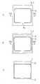
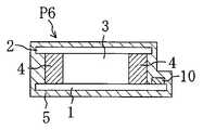
Translated fromKorean도 1은 제 1 실시예의 액정패널(P1)을 개략적으로 나타내는 평면도.1 is a plan view schematically showing a liquid crystal panel P1 of the first embodiment.
도 2는 도 1의 II-II선 단면도.FIG. 2 is a cross-sectional view taken along the line II-II of FIG. 1. FIG.
도 3A, 도 3B 및 도 3C는 액정패널(P1)의 제조공정을 개략적으로 나타내는 평면도.3A, 3B, and 3C are plan views schematically illustrating a manufacturing process of the liquid crystal panel P1.
도 4A, 도 4B 및 도 4C는 액정패널(P1)의 제조공정을 개략적으로 나타내는 단면도이며, 도 4A 및 도 4B는 각각 도 3A에서의 IVA-IVA선 단면도, 도 3B의 IVB-IVB선 단면도.4A, 4B, and 4C are cross-sectional views schematically showing a manufacturing process of the liquid crystal panel P1, and FIGS. 4A and 4B are cross-sectional views taken along the line IVA-IVA in FIG. 3A, and a cross-sectional view taken along the line IVB-IVB in FIG. 3B.
도 5는 제 2 실시예의 액정패널(P2)을 개략적으로 나타내는 단면도.Fig. 5 is a sectional view schematically showing liquid crystal panel P2 of the second embodiment.
도 6은 제 3 실시예의 액정패널(P3)을 개략적으로 나타내는 평면도.6 is a plan view schematically showing liquid crystal panel P3 of the third embodiment.
도 7은 도 6의 VII-VII선 단면도.7 is a cross-sectional view taken along the line VII-VII of FIG. 6.
도 8A 및 도 8B는, 액정패널(P3)의 제조방법을 개략적으로 나타내는 평면도.8A and 8B are plan views schematically showing the manufacturing method of liquid crystal panel P3.
도 9A, 도 9B 및 도 9C는 액정패널(P3)의 제조공정을 개략적으로 나타내는 단면도이며, 도 9A 및 도 9B는 각각 도 8A에서의 IXA-IXA선 단면도, 도 8B의 IXB-IXB선 단면도.9A, 9B and 9C are cross-sectional views schematically showing a manufacturing process of the liquid crystal panel P3, and FIGS. 9A and 9B are cross-sectional views taken along the line IXA-IXA in FIG. 8A, respectively, and taken along the line IXB-IXB in FIG. 8B.
도 10A, 도 10B 및 도 10C는 제 4 실시예의 액정패널 제조공정을 개략적으로 나타내는 단면도.10A, 10B and 10C are cross-sectional views schematically showing a liquid crystal panel manufacturing process of the fourth embodiment.
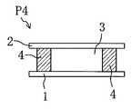
도 11은 제 6 실시예의 액정패널(P4)을 개략적으로 나타내는 평면도.Fig. 11 is a plan view schematically showing liquid crystal panel P4 of the sixth embodiment.
도 12는 도 11의 XII-XII선 단면도.12 is a cross-sectional view taken along the line XII-XII in FIG. 11.
도 13은 도 11의 XIII-XIII선 단면도.13 is a cross-sectional view taken along the line XIII-XIII of FIG. 11.
도 14A, 도 14B 및 도 14C는 액정패널(P4)의 제조공정을 개략적으로 나타내는 평면도.14A, 14B and 14C are plan views schematically showing the manufacturing process of liquid crystal panel P4.
도 15A, 도 15B 및 도 15C는 액정패널(P4)의 제조공정을 개략적으로 나타내는 단면도.15A, 15B and 15C are cross-sectional views schematically showing a manufacturing process of liquid crystal panel P4.
도 16은 제 7 실시예의 액정패널(P5)을 개략적으로 나타내는 평면도.Fig. 16 is a plan view schematically showing liquid crystal panel P5 of the seventh embodiment.
도 17은 도 16의 XVII-XVII선 단면도.17 is a cross-sectional view taken along the line XVII-XVII in FIG. 16.
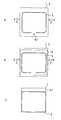
도 18은 제 9 실시예의 액정패널을 개략적으로 나타내는 평면도.18 is a plan view schematically showing the liquid crystal panel of the ninth embodiment;
도 19는 도 18의 XIX-XIX선 단면도.FIG. 19 is a sectional view taken along line XIX-XIX in FIG. 18; FIG.
도 20A 및 도 20B는 제 10 실시예의 액정패널(P6) 제조공정을 개략적으로 나타내는 평면도.20A and 20B are plan views schematically showing a manufacturing process of liquid crystal panel P6 of the tenth embodiment.
도 21A, 도 21B 및 도 21C는 액정패널(P6) 제조공정을 개략적으로 나타내는 단면도이며, 도 21A 및 도 21B는, 각각 도 20A의 XXI A-XXI A선 단면도, 도 20B는 XXI B-XXI B선 단면도.21A, 21B and 21C are cross-sectional views schematically showing a manufacturing process of the liquid crystal panel P6. FIGS. 21A and 21B are cross-sectional views taken along line XXI A-XXI A of FIG. 20A, and FIG. 20B is XXI B-XXI B. FIG. Line section.
본 발명은 표시패널 및 그 제조방법에 관한 것이다. 본 발명의 표시패널은, 액정패널, 플라즈마 표시패널, 일렉트로크로믹 표시패널 등에 적용할 수 있다.The present invention relates to a display panel and a method of manufacturing the same. The display panel of the present invention can be applied to liquid crystal panels, plasma display panels, electrochromic display panels, and the like.
표시장치의 하나인 액정패널을 박형화 하기 위해, 기판의 박막화가 종래부터 연구되고 있다. 현재의 액정패널은 각각의 두께가 3mm~0.4mm인 한 쌍의 유리기판이 일반적으로 사용되며, 이들 기판 사이에 두께 수 미크론의 액정층을 개재하여 구성된다. 두께가 0.4mm보다 얇은 유리기판을 채용하면 기계적 강도가 저하되므로, 사용할 때에 유리기판이 파손되는 등의 문제를 일으킨다.In order to reduce the thickness of a liquid crystal panel, which is one of display devices, thinning of a substrate has been studied in the past. In current liquid crystal panels, a pair of glass substrates each having a thickness of 3 mm to 0.4 mm is generally used, and a liquid crystal layer having a thickness of several microns is interposed between these substrates. If the glass substrate having a thickness of less than 0.4 mm is adopted, the mechanical strength is lowered, which causes problems such as breakage of the glass substrate during use.
일본국 특개평 6-340029호 공보에는, 적어도 1 종 이상의 수지층으로 이루어지는 수지판의 한쪽 면 또는 양면에, 두께가 500㎛ 이하의 유리필름을 적층시킨 적층판이 개시되어 있다. 이 적층판은, 유리 정도의 표면강도와 수지의 열 가공성 및 절단 가공성을 함께 할 뿐 아니라, 내용제성, 제전성(制電性) 등이 유리와 동등한 표면특성을 갖는다.Japanese Laid-Open Patent Publication No. 6-340029 discloses a laminate in which a glass film having a thickness of 500 μm or less is laminated on one or both surfaces of a resin plate composed of at least one or more resin layers. This laminated plate not only combines the surface strength of glass with the heat workability and cutting processability of the resin, but also has surface properties equivalent to those of glass such as solvent resistance, antistatic properties, and the like.
일본국 특개 2001-113631호 공보에는, 두께 0.1㎛ 이상 100㎛ 이하의 유리필름의 적어도 한쪽 면에, 두께 1㎛ 이상 1000㎛ 이하의 플라스틱필름을 적층 고착시킨 플라스틱필름ㆍ유리필름 적층체가 개시되어 있다. 이 적층체는 유리가 갖는 내약품성, 내마모성, 가스방지성 등을 겸비하여, 취급 및 2 차 가공성에 우수하다.Japanese Patent Laid-Open No. 2001-113631 discloses a plastic film / glass film laminate in which a plastic film having a thickness of 1 μm or more and 1000 μm or less is laminated and fixed to at least one surface of a glass film having a thickness of 0.1 μm or more and 100 μm or less. . This laminate has both chemical resistance, abrasion resistance, and gas prevention properties of glass, and is excellent in handling and secondary workability.
일본국 특개 2001-162721호 공보에는, 열경화성 수지제의 본체 표면에 유리필름 또는 유리필름과 수지층으로 이루어지는 피복층이 고착된 열경화성 수지복합품이 개시되어 있다. 또 일본국 특개 2001-162721호 공보의 0041단락에는 유리필름의 두께가 0.1~100㎛가 바람직하며, 0.1~20㎛가 보다 바람직한 것으로 개시되어 있다.Japanese Laid-Open Patent Publication No. 2001-162721 discloses a thermosetting resin composite product in which a coating film made of a glass film or a glass film and a resin layer is fixed to a surface of a thermosetting resin body. In addition, paragraph 0041 of Japanese Patent Laid-Open No. 2001-162721 discloses that the thickness of the glass film is preferably 0.1 to 100 µm, more preferably 0.1 to 20 µm.
상기의 각 공보는, 각 공보에 각각 개시된 적층체(복합품)를 표시장치용 기판으로 이용하는 점에 대해서는 개시되지 않고 있다. 본 발명자들은, 액정패널의 제조라인을 사용하여 이들 적층체(복합품)로 액정패널을 시험 제조한 바, 이하의 식견을 얻었다.Each of the above publications does not disclose the use of a laminate (composite product) disclosed in each publication as a substrate for a display device. MEANS TO SOLVE THE PROBLEM The present inventors obtained the following knowledge, when the liquid crystal panel was test-processed with these laminated bodies (composites) using the manufacturing line of the liquid crystal panel.
첫째로, 액정패널이 제조라인 상에서의 충격에 견디기 위해서는, 유리기판의 양면을 수지로 코팅해야만 한다. 따라서 적층체(복합품)의 총 막 두께가 두꺼워지므로, 표시장치의 박형 경량화를 실현하기가 어렵다. 또 원가도 높아진다.First, in order for the liquid crystal panel to withstand the impact on the manufacturing line, both sides of the glass substrate must be coated with a resin. Therefore, since the total film thickness of a laminated body (composite product) becomes thick, it is difficult to realize thin and light weight of a display apparatus. It also raises costs.
둘째로, 적층시키는 수지의 종류에 따라 내열온도가 다르므로(대략 250℃~300℃), 제조공정에서 적층체(복합품)에 가할 수 있는 열량에 제약이 따른다. 또 유리기판과 수지층의 적층 시나 적층판에의 가열냉각공정에서, 유리와 수지의 열팽창률 차에 의해 적층체(복합품)에 휨이 발생하므로, 불량품 발생률이 높다. 예를 들어 두께 0.2mm 전후의 유리기판 상에 수지층이 적층된 적층기판을 제조라인으로 보낼 경우, 수지의 내열온도 이하의 온도에서도 가열냉각공정을 되풀이함에 따라, 유리와 수지의 열팽창률 차에 의한 기판의 휨이 발생한다. 때문에 기판이 깨지거나, 패터닝 정밀도나 접합정밀도가 저하되는 등의 문제가 발생할 우려가 있다. 따라서 제조라인 상에서의 제약에 의해, 상기 각 공보에 개시된 적층체(복합품)로 액정패널을 제조하는 것은, 양산에 부적합하다.Second, since the heat resistance temperature varies depending on the type of resin to be laminated (about 250 ° C to 300 ° C), there is a restriction on the amount of heat that can be applied to the laminate (composite product) in the manufacturing process. In addition, in the case of lamination of the glass substrate and the resin layer or in the heating and cooling step on the laminated sheet, warpage occurs in the laminate (composite product) due to the difference in thermal expansion coefficient between the glass and the resin, so that the defective product occurrence rate is high. For example, when a laminated substrate having a resin layer laminated on a glass substrate having a thickness of about 0.2 mm is sent to a manufacturing line, the heating and cooling process is repeated even at a temperature below the heat resistance temperature of the resin, and thus the difference in thermal expansion coefficient between the glass and the resin is increased. Warping of the substrate occurs. This may cause problems such as cracking of the substrate and deterioration in patterning accuracy and bonding accuracy. Therefore, it is not suitable for mass production to manufacture a liquid crystal panel by the laminated body (composite product) disclosed by said each publication by the restriction on a manufacturing line.
한편, 일본국 특개 2002-297054호 공보에는, 두께 50~700㎛인 유리층과, 유 리층 양측에 형성된, 소정의 평균 열선 팽창계수를 갖는 수지층(두께 1~7000㎛)으로 이루어지는 적층시트를 사용하여 구성되는 표시소자용 기판이 개시되어 있다. 일본국 특개 2002-297054호 공보에 개시된 표시소자용 기판에 따르면, 유리층과 수지층의 평균 열선 팽창계수 차가 작으므로, 내열성 평가시험에서 수지층에 균열 등의 변화가 관찰되지 않는다. 그러나 이 표시소자용 기판은 유리층 양측에 수지층이 형성되므로, 한 쌍의 표시소자용 기판을 이용하여 액정패널을 제조할 경우 액정패널이 두꺼워지므로, 표시패널의 박형 경량화를 실현하기가 어렵다.On the other hand, Japanese Laid-Open Patent Publication No. 2002-297054 discloses a laminated sheet consisting of a glass layer having a thickness of 50 to 700 µm and a resin layer (1 to 7000 µm in thickness) having a predetermined average thermal expansion coefficient formed on both sides of the glass layer. Disclosed is a substrate for a display element constructed using. According to the substrate for display elements disclosed in Japanese Patent Laid-Open No. 2002-297054, since the difference in average thermal radiation coefficient between the glass layer and the resin layer is small, no change in cracks or the like is observed in the resin layer in the heat resistance evaluation test. However, since the resin layer is formed on both sides of the glass layer in this display element substrate, when the liquid crystal panel is manufactured by using a pair of display element substrates, the liquid crystal panel becomes thick, and thus it is difficult to realize a thin and light display panel.
본 발명은 제조라인 상에서의 제약을 받는 일없이, 표시패널의 박형 경량화를 실현하는 것을 목적으로 한다.An object of the present invention is to realize a thin and light display panel without being restricted on a manufacturing line.
본 발명의 제 1 국면에 의한 표시패널은, 각각의 두께가 0.15mm 이상 0.3mm 이하인 한 쌍의 유리기판과, 상기 한 쌍의 유리기판을 접합하는 시일 부재를 구비하는 표시패널로서, 상기 한 쌍의 유리기판 중 적어도 한쪽 유리기판의 외측면에는, 수지층이 적층된다.A display panel according to the first aspect of the present invention is a display panel comprising a pair of glass substrates each having a thickness of 0.15 mm or more and 0.3 mm or less and a sealing member for joining the pair of glass substrates, wherein the pair is a display panel. The resin layer is laminated on the outer surface of at least one glass substrate of the glass substrates.
상기의 표시패널에서는, 1 매 또는 2 매의 유리기판 외측면만을 수지로 피복함으로써, 표시패널의 기계적 강도가 높아진다. 이는 대향하는 2 매의 유리기판이 시일 부재로 접합되므로, 표시패널의 가장 외표면만을 수지로 강화시킴으로써, 외적인 스트레스에 대해 충분한 강도를 확보할 수 있기 때문이다. 따라서 상기의 표시패널에 의하면, 2 매의 유리기판 각각의 양면을 강화시키는 경우에 비해 수지층의 총 막 두께가 얇아지므로, 표시패널의 박형 경량화를 실현할 수 있다. 또 제조라인에서의 충격에 견딜 수 있을 정도의 기계적 강도를 가지므로, 제조라인에 의한 양산에 적합하다.In the above display panel, the mechanical strength of the display panel is increased by coating only one or two glass substrate outer surfaces with resin. This is because two opposing glass substrates are joined by a sealing member, so that only the outermost surface of the display panel can be reinforced with a resin, thereby ensuring sufficient strength against external stress. Therefore, according to the above display panel, the total film thickness of the resin layer becomes thinner than the case where both surfaces of each of the two glass substrates are reinforced, so that the display panel can be made thinner and lighter. Moreover, since it has mechanical strength enough to withstand the impact in a manufacturing line, it is suitable for the mass production by a manufacturing line.
상기 수지층은, 주로 유기수지로 구성되는 층이라도 좋다. 이로써 유리기판이 노출된 것과 비교해 내마모성이 향상되므로, 표시패널의 표면이 손상되기 어려워진다. 또 유리기판에 유기수지층을 적층시킴으로써 곡률이 비교적 작은 형상을 갖는 유리기판에도 대응할 수 있어, 유연하면서 강도있는 수지-유리 적층판이 형성된다.The resin layer may be a layer mainly composed of an organic resin. As a result, the wear resistance is improved compared to that of the glass substrate exposed, which makes it difficult to damage the surface of the display panel. In addition, by laminating the organic resin layer on the glass substrate, it is possible to cope with a glass substrate having a relatively small curvature, thereby forming a flexible and rigid resin-glass laminate.
상기 수지층은, 무기 콜로이드 입자와 유기 바인더수지로 구성되는 하이브리드 재료를 포함해도 된다. 하이브리드 재료를 포함하는 무기-유기 복합박막은, 유기성만이 아닌 무기성도 띄므로, 탄성률이나 경도 등의 역학특성이 향상되어, 내열성이나 내약품성이 비약적으로 향상된다.The resin layer may contain a hybrid material composed of inorganic colloidal particles and an organic binder resin. Since the inorganic-organic composite thin film containing a hybrid material is not only organic but also inorganic, the mechanical properties such as elastic modulus and hardness are improved, and the heat resistance and chemical resistance are remarkably improved.
상기 수지층은 두께가 2㎛ 이상 50㎛ 이하인 것이 바람직하다. 0.15mm 이상 0.3mm 이하의 박막화된 유리기판에 대해 충분한 기계적 강도가 확보됨과 동시에, 2차 가공성도 향상되어 박형 경량화가 가능해진다.It is preferable that the said resin layer is 2 micrometers or more and 50 micrometers or less in thickness. Sufficient mechanical strength is ensured for the thinned glass substrate of 0.15 mm or more and 0.3 mm or less, and the secondary workability is also improved to enable thin and light weight.
상기 한 쌍의 유리기판 중의 한쪽 유리기판은, 그 내측면에 있어, 상기 시일 부재보다 바깥쪽에 형성된 단자부를 구비하고, 상기 단자부에는 수지층이 형성돼도 된다. 표시패널에서 단자부는, 시일 부재보다 외측에 위치하는 1 매의 유리판이므로 구조적으로 스트레스에 가장 약하다. 단자부에도 수지층을 적층시킴으로써, 바꾸어 말하면 단자부만을 양면 수지코팅 함으로써, 구조적으로 스트레스에 가장 약한 단자부를 효과적으로 강화시키기가 가능해진다.One glass substrate of the pair of glass substrates may have a terminal portion formed on the inner side of the pair of glass substrates outside the seal member, and a resin layer may be formed on the terminal portion. In the display panel, the terminal portion is one of the glass plates positioned outside the sealing member, and thus, the terminal portion is structurally the weakest in stress. By laminating a resin layer on the terminal part, in other words, by coating only the terminal part on both sides, it is possible to effectively reinforce the terminal part which is structurally weakest to stress.
상기 단자부에는 집적회로 칩이 실장되며, 상기 단자부와 상기 집적회로 칩 의 접속부분이 적어도 수지로 피복되는 것이 바람직하다. 이로써 단자와 집적회로 칩의 접속부분이 수지코팅으로 보강되므로, 접속신뢰성이 향상된다.An integrated circuit chip is mounted on the terminal portion, and the connection portion between the terminal portion and the integrated circuit chip is preferably covered with at least resin. As a result, the connection between the terminal and the integrated circuit chip is reinforced with resin coating, thereby improving connection reliability.
상기 한 쌍의 유리기판 중 적어도 한쪽 유리기판의 내측면에는 편광층이 적층되어도 좋다. 이로써 한 쌍의 기판 사이에 액정층 등의 광변조층이 개재할 경우, 에칭에 의한 유리두께의 공차나 수지층의 두께 공차에 의한 리타데이션 변화를 억제할 수 있다. 또 유리기판 강도의 향상을 도모할 수도 있다.The polarizing layer may be laminated on at least one inner surface of the pair of glass substrates. Thereby, when light modulation layers, such as a liquid crystal layer, are interposed between a pair of board | substrates, the retardation change by the tolerance of the glass thickness by etching and the thickness tolerance of a resin layer can be suppressed. In addition, the strength of the glass substrate can be improved.
본 발명의 제 2 국면에 의한 표시패널은, 각각의 두께가 0.15mm 이상 0.3mm 이하인 한 쌍의 유리기판과, 상기 한 쌍의 유리기판을 접합하는 시일 부재를 구비하는 표시패널로서, 상기 한 쌍의 유리기판의 단면은, 적어도 일부가 수지층을 갖는다.A display panel according to a second aspect of the present invention is a display panel comprising a pair of glass substrates each having a thickness of 0.15 mm or more and 0.3 mm or less and a sealing member for bonding the pair of glass substrates, wherein the pair At least a portion of the cross section of the glass substrate has a resin layer.
본 발명의 제 2 국면에 의한 표시패널에서는, 단면 중 적어도 일부가 수지로 피복됨으로써 표시패널의 기계적 강도가 높아진다. 이는 구조적으로 스트레스에 가장 약한, 표시패널 단부가 수지코팅 됨으로써, 강도가 향상되기 때문이다. 따라서 본 발명의 제 2 국면에 의한 표시패널에 의하면, 2 매의 유리기판 각각의 양면을 강화시키는 경우에 비해 표시패널의 총 두께가 얇아지므로, 표시패널의 박형 경량화를 실현할 수 있다. 또 제조라인에서의 충격에 견딜 수 있을 정도의 기계적 강도를 가지므로, 제조라인에 의한 양산에 적합하다.In the display panel according to the second aspect of the present invention, the mechanical strength of the display panel is increased by covering at least a part of the cross section with a resin. This is because the strength of the display panel, which is structurally weakest in stress, is improved by resin coating. Therefore, according to the display panel according to the second aspect of the present invention, the total thickness of the display panel is thinner than the case where both surfaces of each of the two glass substrates are reinforced, so that the display panel can be made thinner and lighter. Moreover, since it has mechanical strength enough to withstand the impact in a manufacturing line, it is suitable for the mass production by a manufacturing line.
본 발명의 제 2 국면에 의한 표시패널에 있어서, 상기 시일 부재는 상기 수지층으로 폐쇄된 주입구를 구비해도 좋다. 이로써 표시패널 단부의 강도가 향상될 뿐만 아니라, 시일 부재의 주입구가 폐쇄되어 액정재료 등의 표시매체가 주입구로 부터 누출되는 것을 방지할 수 있다. 또 주입구에 밀봉이 형성돼 있을 경우, 제조라인에서의 충격에 의해 밀봉이 어긋나거나, 박리되거나 하여 표시매체가 주입구로부터 누출될 우려가 있다. 그러나 시일 부재의 주입구를 수지로 피복함으로써 밀봉이 어긋나는 등의 경우에도 표시매체가 주입구로부터 누출되는 것을 막을 수 있다.In the display panel according to the second aspect of the present invention, the seal member may include an injection port closed by the resin layer. As a result, not only the strength of the end portion of the display panel is improved, but also the injection hole of the seal member is closed to prevent the display medium such as the liquid crystal material from leaking from the injection hole. In addition, when a seal is formed in the injection hole, the sealing medium may be displaced or peeled off due to an impact on the manufacturing line, and the display medium may leak from the injection hole. However, by covering the injection hole of the seal member with resin, it is possible to prevent the display medium from leaking from the injection hole even in the case where the sealing is deviated.
본 발명의 제 2 국면에 의한 표시패널에 있어서, 상기 한 쌍의 유리기판 각각은, 수지층이 적층된 외측면을 갖는 것이 바람직하다. 또한 표시패널 전면이 수지층으로 피복되는 것이 바람직하다. 이로써 우수한 기계적 강도 및 높은 신뢰성을 실현할 수 있다. 또 2 매의 유리기판 각각의 양면을 강화시키는 경우에 비해 표시패널의 총 두께가 얇아지므로, 표시패널의 박형 경량화를 실현할 수 있다.In the display panel according to the second aspect of the present invention, each of the pair of glass substrates preferably has an outer surface on which a resin layer is laminated. It is also preferable that the entire display panel is covered with a resin layer. As a result, excellent mechanical strength and high reliability can be realized. In addition, since the total thickness of the display panel becomes thinner than when the two surfaces of each of the two glass substrates are strengthened, the thickness of the display panel can be reduced.
본 발명의 제 1 국면에 의한 방법은, 본 발명의 제 1 국면에 의한 표시패널을 제조하는 방법으로서, 상기 시일 부재를 개재하고, 각각의 두께가 0.3mm보다 두꺼운 한 쌍의 유리기판을 접합하는 공정과, 접합된 상기 한 쌍의 유리기판 각각을 두께가 0.15mm 이상 0.3mm 이하로 될 때까지 박막화하는 공정과, 박막화된 상기 한 쌍의 유리기판 중 적어도 한쪽 유리기판의 외측면에, 상기 수지층을 형성하는 공정을 포함한다.The method according to the first aspect of the present invention is a method of manufacturing the display panel according to the first aspect of the present invention, wherein a pair of glass substrates each having a thickness greater than 0.3 mm are bonded through the seal member. And thinning each of the bonded pairs of glass substrates until the thickness becomes 0.15 mm or more and 0.3 mm or less, and at the outer side of at least one glass substrate of the paired thin glass substrates, It includes the process of forming a strata.
이 제조방법에 의하면, 수지층 형성공정 전에 접합공정이 실시되므로, 제조공정에서 가할 수 있는 열량의 제약이 완화된다. 또 유리기판과 수지층의 적층 시에, 혹은 프레스공정 등의 적층기판에의 가열공정에서, 유리와 수지(예를 들어 플라스틱)의 열팽창률 차에 의해 발생하는 적층기판의 휨이 해소된다. 또한 접합공 정에서 위치조정 정밀도 저하 등의 문제를 회피할 수 있다. 따라서 박형의 수지(예를 들어 플라스틱필름) 강화 유리 기판을 용이하게 형성할 수 있다.According to this manufacturing method, since the joining step is performed before the resin layer forming step, the restriction of the amount of heat that can be applied in the manufacturing step is alleviated. In addition, when the glass substrate and the resin layer are laminated or in a heating step to a laminated substrate such as a press step, the warpage of the laminated substrate caused by the difference in thermal expansion coefficient between the glass and the resin (for example, plastic) is eliminated. In addition, problems such as a decrease in positioning accuracy in the joining process can be avoided. Therefore, a thin resin (for example, plastic film) tempered glass substrate can be easily formed.
상기 박막화 공정은, 화학적 에칭공정 또는 물리적 연마공정을 포함하는 것이 바람직하다.It is preferable that the said thinning process includes a chemical etching process or a physical polishing process.
본 발명의 제 2 국면에 의한 방법은, 각각의 두께가 0.15mm 이상 0.3mm 이하인 한 쌍의 유리기판과, 상기 한 쌍의 유리기판을 접합하는 시일 부재를 구비하며, 양면에 수지층이 적층되는 표시패널을 제조하는 방법으로서, 상기 수지층을 개재하고, 상기 유리기판과 지지기판을 접합함으로써 한 쌍의 적층판(유리-수지-유리)을 형성하는 공정과, 상기 지지기판을 바깥쪽으로 하여, 상기 시일 부재를 개재하고, 상기 한 쌍의 적층판을 접합하는 공정과, 접합된 상기 한 쌍의 적층판인 상기 지지기판을 화학적 에칭으로 제거하는 공정을 포함한다.The method according to the second aspect of the present invention comprises a pair of glass substrates each having a thickness of 0.15 mm or more and 0.3 mm or less, and a seal member for joining the pair of glass substrates, wherein a resin layer is laminated on both surfaces. A method of manufacturing a display panel, comprising: forming a pair of laminated plates (glass-resin-glass) by bonding the glass substrate and a support substrate through the resin layer, and with the support substrate facing outward, And a step of joining the pair of laminated plates via a seal member, and removing the support substrate, which is the pair of laminated plates, joined by chemical etching.
상기 지지기판은 두께가 0.5mm 이상인 것이 바람직하며, 0.7mm 이상이 보다 바람직하다. 상기 수지층은 두께가 2㎛ 이상 50㎛ 이하인 것이 바람직하다. 상기 수지층은, 주로 유기수지로 구성되는 층, 또는 무기 콜로이드 입자와 유기 바인더수지로 구성되는 하이브리드 재료를 포함하는 층인 것이 바람직하다.The support substrate preferably has a thickness of 0.5 mm or more, more preferably 0.7 mm or more. It is preferable that the said resin layer is 2 micrometers or more and 50 micrometers or less in thickness. It is preferable that the said resin layer is a layer mainly comprised from an organic resin, or a layer containing the hybrid material comprised from inorganic colloidal particle and organic binder resin.
이 제조방법에 의하면, 적층기판이 충분히 두꺼우므로, 제조라인 상에서의 기계적 강도가 확보된다. 또 지지기판을 충분히 두껍게 할 수 있으므로, 열팽창률 차에 의한 기판의 휨을 억제할 수 있다. 바꾸어 말하면 온도제약을 받지 않는다. 따라서 시일 부재를 개재하고 안정되게 접합시키기가 가능해진다. 또한 접합 후에 화학적 에칭으로 지지기판을 제거할 경우 수지층이 에칭스토퍼로서 작용하므로, 수 지층-유리기판의 총 막 두께를 균일화시키는 것도 가능하다.According to this manufacturing method, since the laminated substrate is sufficiently thick, mechanical strength on the production line is secured. In addition, since the support substrate can be sufficiently thick, the warpage of the substrate due to the difference in thermal expansion rate can be suppressed. In other words, they are not subject to temperature constraints. Therefore, it becomes possible to stably join through a sealing member. In addition, since the resin layer acts as an etching stopper when the support substrate is removed by chemical etching after bonding, it is possible to equalize the total film thickness of the resin layer-glass substrate.
본 발명의 제 3 국면에 의한 방법은, 각각의 두께가 0.15mm 이상 0.3mm 이하인 한 쌍의 유리기판과, 상기 한 쌍의 유리기판을 접합하는 시일 부재와, 상기 한 쌍의 유리기판 및 상기 시일 부재가 형성하는 틈새 내에 충전된 액정재료를 구비하는 표시패널을 제조하는 방법으로서, 주입구를 갖는 상기 시일 부재를 개재하고, 각각의 두께가 0.3mm보다 두꺼운 한 쌍의 유리기판을 접합하는 공정과, 접합된 상기 한 쌍의 유리기판을 분단시켜, 상기 시일 부재의 주입구를 상기 한 쌍의 유리기판 단면에 노출시키는 공정과, 상기 한 쌍의 유리기판 각각을 두께가 0.15mm 이상 0.3mm 이하로 될 때까지 박막화하는 공정과, 상기 주입구에서 상기 틈새 내로 상기 액정재료를 충전시키는 공정과, 상기 한 쌍의 유리기판 단면 중, 적어도 상기 주입구 부분의 단면에 수지층을 형성하는 공정을 포함한다.The method according to the third aspect of the present invention comprises a pair of glass substrates each having a thickness of 0.15 mm or more and 0.3 mm or less, a seal member for bonding the pair of glass substrates, the pair of glass substrates and the seal A method of manufacturing a display panel comprising a liquid crystal material filled in a gap formed by a member, the method comprising: bonding a pair of glass substrates each having a thickness greater than 0.3 mm via the seal member having an injection hole; Exposing the bonded pair of glass substrates to expose the inlet of the sealing member to the pair of glass substrate cross-sections, and when each of the pair of glass substrates has a thickness of 0.15 mm or more and 0.3 mm or less. Forming a resin layer on at least an end face of the injection hole section of the pair of glass substrates; And a step of.
이 제조방법에 의하면, 단부의 기계적 강도가 향상된 액정패널을 용이하게 제조할 수 있다. 또 적어도 주입구 부분의 단면을 수지로 피복함으로써, 단부의 기계적 강도를 향상시킬 수 있음과 동시에, 시일 부재의 주입구를 막을 수 있으므로 공정 수의 증가를 억제할 수 있어, 고 효율화나 저 원가화가 실현된다. 유리모기판으로부터 다수의 액정패널을 취하는 설계일 경우는, 주입구 노출 및 단 셀화(단자 노출)의 분단공정을 1 공정으로 실시하기가 가능해져, 분단에 따른 스트레스도 대폭 경감시킬 수 있다. 이 제조방법에 의하면 분단공정 후에 박막화공정을 실시하므로, 박막화된 유리기판을 분단시키는 경우보다 불량품 발생을 억제할 수 있다.According to this manufacturing method, a liquid crystal panel with improved mechanical strength at the end can be easily manufactured. In addition, by covering at least the end face of the injection port portion with a resin, the mechanical strength of the end portion can be improved, and the injection port of the seal member can be blocked, so that an increase in the number of steps can be suppressed, resulting in high efficiency and low cost. . In the case of designing a plurality of liquid crystal panels from a glass mother substrate, it is possible to perform the dividing step of the injection hole exposure and the single cell (terminal exposure) in one step, and the stress due to the division can be greatly reduced. According to this manufacturing method, since the thinning step is performed after the dividing step, the occurrence of defective products can be suppressed more than when the thinned glass substrate is divided.
본 발명의 제 4 국면에 의한 방법은, 각각의 두께가 0.15mm 이상 0.3mm 이하인 한 쌍의 유리기판과, 상기 한 쌍의 유리기판을 접합하는 시일 부재와, 상기 한 쌍의 유리기판 및 상기 시일 부재가 형성하는 틈새 내에 충전된 액정재료를 구비하는 표시패널을 제조하는 방법으로서, 각각의 두께가 0.3mm보다 두꺼운 한 쌍의 유리기판 중 한쪽 유리기판에, 상기 시일 부재를 형성하는 공정과, 상기 시일 부재 안쪽으로 상기 액정재료를 적하시키는 공정과, 상기 시일 부재를 개재하고 상기 한 쌍의 유리기판을 접합하는 공정과, 접합된 상기 한 쌍의 유리기판 각각을 두께가 0.15mm 이상 0.3mm 이하로 될 때까지 박막화하는 공정과, 상기 한 쌍의 유리기판 단면 중, 적어도 일부에 수지층을 형성하는 공정을 포함한다.The method according to the fourth aspect of the present invention comprises a pair of glass substrates each having a thickness of 0.15 mm or more and 0.3 mm or less, a seal member for joining the pair of glass substrates, the pair of glass substrates and the seal A method of manufacturing a display panel comprising a liquid crystal material filled in a gap formed by a member, comprising the steps of: forming the seal member on one glass substrate of a pair of glass substrates each having a thickness greater than 0.3 mm; Dropping the liquid crystal material into the seal member; bonding the pair of glass substrates through the seal member; and bonding the pair of glass substrates to a thickness of 0.15 mm or more and 0.3 mm or less. And forming a resin layer on at least a portion of the pair of glass substrate cross-sections until the film is thinned.
이 제조방법에 의하면, 단부의 기계적 강도가 향상된 액정패널을 용이하게 제조할 수 있다. 또 유리기판을 박막화하기 전에 액정재료가 주입 밀봉된다. 따라서 외적인 스트레스에 의한 기판의 파손 등을 방지할 수 있으므로, 수율을 떨어트리는 일없이 용이하게 박형 액정패널을 제조할 수 있다.According to this manufacturing method, a liquid crystal panel with improved mechanical strength at the end can be easily manufactured. In addition, the liquid crystal material is injection-sealed before thinning the glass substrate. Therefore, since the damage of the board | substrate etc. by external stress can be prevented, a thin liquid crystal panel can be manufactured easily, without falling a yield.
상기 박막화공정은, 화학적 에칭공정 또는 물리적 연마공정을 포함하는 것이 바람직하다.It is preferable that the said thinning process includes a chemical etching process or a physical polishing process.
상기 수지층 형성공정은, 상기 한 쌍의 유리기판 단면 및 외측면을 수지로 피복하는 공정을 포함하는 것이 바람직하다. 이 제조방법에 의하면, 한 쌍의 유리기판의 단면 및 외측면, 바꾸어 말하면 표시패널의 외주면 전면에 수지층을 형성하기 전에 접합공정이 실시되므로, 제조공정에서 가할 수 있는 열량 제약이 완화된다. 또 유리기판과 수지층의 적층 시에, 혹은 프레스공정 등의 적층기판에의 가열 공정에서, 유리와 수지(예를 들어 플라스틱)의 열팽창률 차에 의해 발생하는 적층기판의 휨이 해소된다. 또한 접합공정에서 위치조정 정밀도 저하 등의 문제를 회피할 수 있다. 따라서 박형의 수지(예를 들어 플라스틱필름)강화유리 기판을 용이하게 형성할 수 있다.The resin layer forming step preferably includes a step of covering the pair of glass substrate end surfaces and the outer surface with a resin. According to this manufacturing method, the bonding step is performed before the resin layer is formed on the cross-section and the outer surface of the pair of glass substrates, in other words, the entire outer circumferential surface of the display panel, thereby alleviating the heat restriction that can be applied in the manufacturing process. In addition, when the glass substrate and the resin layer are laminated or in a heating step such as a pressing step, the warpage of the laminated substrate caused by the difference in thermal expansion coefficient between the glass and the resin (for example, plastic) is eliminated. In addition, problems such as a decrease in positioning accuracy in the joining process can be avoided. Therefore, a thin resin (for example, plastic film) tempered glass substrate can be easily formed.
상술한 목적 및 기타의 목적과 본 발명의 특징 및 이점은 첨부 도면과 관련한 다음의 상세한 설명을 통해 보다 분명해 질 것이다.The above and other objects and features and advantages of the present invention will become more apparent from the following detailed description taken in conjunction with the accompanying drawings.
이하 도면을 참조하면서 본 발명의 실시예를 설명한다. 이하의 실시예에서는, 표시패널로서 액정패널을 예로 하여 설명하지만, 본 발명의 표시패널은 액정패널 이외의 다른 표시패널에 적용할 수 있다. 구체적으로는 표시매체로서 액정재료 이외의 광학매체를 채용한 표시소자, 예를 들어 플라즈마 표시패널(PDP), 무기 또는 유기 EL(일렉트로루미네센스) 표시패널, 일렉트로크로믹표시(ECD)패널, 전기영동 표시패널 등의 표시패널에 적용할 수 있다. 또 본 발명의 표시패널은 입체영상표시장치에 이용되는 패럴랙스 배리어(parallax barrier: 시차 세로격자열) 소자나 화상시프트소자에 이용되는 액정소자로서 이용할 수도 있다. 그리고 입체영상표시장치는, 예를 들어 좌안용 화소부 및 우안용 화소부를 갖는 영상표시소자와, 패럴랙스 배리어소자를 포함한다. 또 화상시프트소자는 액정소자와 복굴절소자를 포함한다.An embodiment of the present invention will be described below with reference to the drawings. In the following embodiments, the liquid crystal panel is described as an example of the display panel, but the display panel of the present invention can be applied to other display panels other than the liquid crystal panel. Specifically, a display element employing an optical medium other than a liquid crystal material as the display medium, for example, a plasma display panel (PDP), an inorganic or organic EL (electroluminescence) display panel, an electrochromic display (ECD) panel, It can be applied to display panels such as electrophoretic display panels. The display panel of the present invention can also be used as a parallax barrier device used in a stereoscopic image display device or a liquid crystal device used in an image shift device. The stereoscopic image display apparatus includes, for example, an image display element having a left eye pixel portion and a right eye pixel portion, and a parallax barrier element. The image shift element includes a liquid crystal element and a birefringent element.
(제 1 실시예)(First embodiment)
도 1은 제 1 실시예의 액정패널을 개략적으로 나타내는 평면도이며, 도 2는 도 1의 II-II선 단면도이다. 이 액정패널(P1)은, COG(Chip On Glass)방식으로 액정패널(P1)에 베어칩 실장되는 액정구동용 IC칩(이하, "구동용IC"라 칭함)(10)을 구비한다.1 is a plan view schematically illustrating the liquid crystal panel of the first embodiment, and FIG. 2 is a cross-sectional view taken along the line II-II of FIG. 1. The liquid crystal panel P1 includes a liquid crystal drive IC chip (hereinafter referred to as "drive IC") 10 which is bare-chip mounted on the liquid crystal panel P1 by a COG (Chip On Glass) method.
액정패널(P1)은 스위칭소자가 형성된 소자기판(1)과, 소자기판(1)에 대향 배치된 대향기판(2)과, 양 기판(1, 2) 사이에 개재하는 액정층(3)을 구비한다. 양 기판(1, 2)은, 시일 부재(4)를 개재하여 접합된다. 소자기판(1)의 액정층(3)측의 면(내측면)에는, 매트릭스형으로 배치된 복수의 화소전극(도시 생략)이 형성되고, 대향기판(2)의 액정층(3)측의 면(내측면)에는, 공통전극(도시 생략)이 형성된다. 매트릭스형으로 배치된 복수의 화소전극은, 각각의 전압인가를 제어하는 TFT(Thin Film Transistor)에 접속된다. TFT는, 구동용IC(10)에 접속된 소스배선이나 게이트배선과 접속된다. 구동용IC(10)로부터의 게이트신호에 의해 TFT 스위칭이 제어되어, 매트릭스형으로 배치된 복수의 화소전극으로의 전압인가가 제어된다. 이로써 화소별로 액정층(3)의 투과율이 제어되어 계조표시가 이루어진다.The liquid crystal panel P1 includes an
소자기판(1) 및 대향기판(2) 각각은, 두께가 0.15mm 이상 0.3mm 이하의 유리기판이다. 양 기판(1, 2) 중 적어도 한쪽 기판은, 액정층(3)에 대해 반대쪽 면(외측면)이 수지층(5)으로 피복된다. 본 실시예에서는 양 기판(1, 2) 외측면에 수지층(5)이 각각 형성된다.Each of the
소자기판(1)의 내측면에는 시일 부재(4)보다 외측에 단자(도시 생략)가 형성된다. 단자는 소자기판(1)에 형성된 소스배선이나 게이트배선 등에 접속된다. 이 단자에 구동용IC(10)의 범프가 접합됨으로써, 구동용IC(10)가 액정패널(P1)에 베어 칩 실장된다. 시일 부재(4)보다 외측이며, 단자가 형성된 영역 및 그 근방영역의 소자기판(1) 부분을, 이하에서는 단자부(1a)라 부른다.Terminals (not shown) are formed on the inner side of the
다음으로, 본 실시예의 액정패널(P1)의 제조공정에 대해 도면을 참조하여 설명한다. 도 3A, 도 3B 및 도 3C는 액정패널(P1)의 제조공정을 개략적으로 나타내는 평면도이다. 도 4A, 도 4B 및 도 4C는 액정패널(P1)의 제조공정을 개략적으로 나타내는 단면도이다. 도 4A 및 도 4B는 각각 도 3A의 IVA-IVA선 단면도, 도 3B의 IVB-IVB선 단면도이다.Next, the manufacturing process of liquid crystal panel P1 of a present Example is demonstrated with reference to drawings. 3A, 3B, and 3C are plan views schematically illustrating a manufacturing process of the liquid crystal panel P1. 4A, 4B, and 4C are cross-sectional views schematically illustrating a manufacturing process of the liquid crystal panel P1. 4A and 4B are cross-sectional views taken along the line IVA-IVA of FIG. 3A, and taken along the line IVB-IVB of FIG. 3B, respectively.
우선 두께 0.4mm의 소다유리기판 상에, TFT소자, 소스배선, 게이트배선, ITO(Indium Tin Oxide) 등으로 구성되는 화소전극 및 이들을 피복하는 배향막을 형성하고(모두 도시 생략), 배향막에 러빙처리를 하여 소자기판(1)을 형성한다. 또 두께 0.4mm의 다른 소다유리기판 상에, 컬러필터층 및 배향막을 형성하고(모두 도시 생략), 배향막에 러빙처리를 하여 대향기판(2)을 형성한다.First, a pixel electrode composed of a TFT element, a source wiring, a gate wiring, an ITO (Indium Tin Oxide), or the like and an alignment film covering them are formed on a soda glass substrate having a thickness of 0.4 mm (both not shown), and rubbing treatment is performed on the alignment film. To form the
소자기판(1) 상의 주변에, 표시영역을 둘러싸는 시일 부재(4)를 형성한다. 시일 부재(4)는, 디스펜서를 이용하여 시일 패턴을 기판(1) 상에 묘화하는 디스펜서 방식, 또는 패터닝된 시일 패턴을 인쇄하는 스크린 인쇄방식에 의해 형성할 수 있다. 시일 부재(4)로는 열경화형이나 자외선 경화형의 수지가 사용된다. 양 기판(1, 2)의 위치조정 후, 시일 부재(4)를 개재시켜 양 기판(1, 2)을 중첩시킨다. 양 기판(1, 2)에 압력을 가하면서 가열 또는 자외선을 조사하여 양 기판(1, 2)을 접합한다(도 3A 및 도 4A 참조). 여기서 시일 부재(4)는 액정재료를 주입하기 위한 주입구(4a)를 갖는다.In the periphery on the
양 기판(1, 2) 사이의 주연부에, 디스펜서를 이용하여 UV(자외선)경화형 접착재료(6)를 침투시킨다. UV조사장치에 의해 접착재료(6)를 경화시키고, 기판내부를 밀봉하여 외부로부터 차단시킨다(도 3B 및 도 4B 참조).A UV (ultraviolet) curable
양 기판(1, 2)의 외측면을 불산에 의한 화학적 에칭으로, 양 기판(1, 2)을 박막화한다. 박막화는, 각각의 기판(1, 2) 두께가 0.1mm 이상 0.3mm 이하로 될 때까지, 바꾸어 말하면 접합된 적층체 두께가 대략 0.2mm 이상 0.6mm 이하로 될 때까지 실시한다. 여기서 본 실시예에서는 화학적 에칭에 의해 박막화를 실시하는 경우에 대해 설명하지만, 물리적 연마에 의해 박막화시켜도 된다. 물리적 연마에 의한 경우, UV경화형 접착재료(6)로 기판 에지를 밀봉하는 공정은 필요 없다.The outer surfaces of both
열 경화형 수지재료로서 아크릴계 수지를 이용하여, 스핀코터로 수지재료를 양 기판(1, 2) 외측면에 도포한다. 약 200℃에서 열처리를 함으로써, 두께 1㎛ 이상 100㎛ 이하, 바람직하게는 2㎛ 이상 50㎛ 이하의 수지층(5)을 형성하여 액정패널(P1)을 형성한다(도 4C 참조).Acrylic resin is used as the thermosetting resin material, and the resin material is applied to the outer surfaces of both
본 실시예에서는 열 경화형 수지를 이용하지만, UV(자외선)경화형 수지를 이용하여 수지층(5)을 형성해도 된다. 수지 종류로는, 에폭시수지, PES(폴리에테르설폰)수지, 우레탄수지, 초산비닐수지 등의 유기수지를 들 수 있다. 수지층(5)은 주로 유기재료로 구성된다. 또 유기수지 대신 유리기판에 대해 밀착성이 높은 하이브리드 재료를 이용하는 것이 바람직하다. 하이브리드 재료를 이용함으로써 탄성률이나 경도 등의 역학특성이 향상되며, 내열성이나 내약품성이 비약적으로 향상된다. 하이브리드 재료는, 무기 콜로이드입자와 유기 바인더수지로 구성된다. 예 를 들어 실리카 등의 무기 콜로이드입자와, 에폭시수지, 폴리우레탄 아크릴레이트수지나 폴리에스텔 아크릴레이트수지 등의 유기 바인더수지로 구성된다.In the present embodiment, a thermosetting resin is used, but the
수지층(5)을 형성한 후, 액정패널(P1)을 소정 크기로 분단 가공하고, 접착재료(6)에 의한 접합부분을 제거한다. 또 시일 부재(4)의 주입구(4a)를 양 기판(1, 2) 단면에 노출시킨다. 분단 가공이란, 유리기판 표면에 스크라이브 선을 긋고, 스크라이브 선을 따라 유리기판을 분단(breaking)하는 것이다. 분단가공 후, 소자기판(1)의 단자부(1a)에 대향하는 대향기판 부분을 분단으로써 제거하여, 단자부(1a)의 내측면을 노출시킨다(도 3C 참조). 이하, 단자부(1a)의 내측면을 노출시키는 것을 "단자노출"이라고도 한다.After the
시일 부재(4)의 주입구(4a)로부터 액정재료를 주입시켜, 양 기판(1, 2) 사이에 액정층(3)을 형성한다. 액정재료 주입은, 디스펜서 방식 또는 딥핑방식으로 실시할 수 있다. 액정재료를 주입한 후, 주입구(4a)를 밀봉(7)로 밀봉한다. 구체적으로는 디스펜서를 이용하여, 열 경화형 또는 UV경화형 수지를 주입구(4a)에 도포하고, 가열 또는 자외선 조사로 경화시킨다. 그 후 소자기판(1)의 단자부(1a) 내측면에, 구동용IC(10)를 베어칩 실장함으로써, 본 실시예의 액정패널(P1)이 형성된다(도 1 참조).The liquid crystal material is injected from the
(시험예)(Test example)
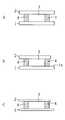
유리기판 및 수지층의 두께를 여러 가지로 변경한 액정패널을 형성했다. 이들 액정패널을 이용하여 분단가공 및 단자노출을 실시할 때의 균열 발생 등을 조사했다. 그 결과를 표 1에 종합하여 나타낸다.The liquid crystal panel which changed the thickness of a glass substrate and the resin layer in various ways was formed. Using these liquid crystal panels, cracks and the like during division processing and terminal exposure were investigated. The result is put together in Table 1, and is shown.
표 1Table 1

표 1 에서 "X"는 발생한 것을, "O"는 발생하지 않은 것을 각각 나타낸다.In Table 1, "X" represents that has occurred and "O" has not occurred.
수지층이 없는 액정패널에서는 유리기판의 두께가 0.25mm 이하의 경우, 기판이 지나치게 얇기 때문에, 분단가공을 실시할 때 분단 정밀도를 얻지 못하고 기판에 균열이 생겼다. 또 단자부의 기계적 강도가 낮으므로, 단자노출 시에 단자부가 파손됐다(표 1 중의 ① 참조). 유리기판의 두께가 0.30mm의 경우, 유리기판이 두꺼우므로 분단가공 시, 기판에 균열은 발생하지 않았다. 그러나 단자노출에서 단자부가 파손됐다(표 1 중의 ② 참조). 유리기판의 두께가 0.35mm 이상의 경우, 분단가공 시, 기판에 균열은 발생하지 않았다. 또 단자노출에 있어서 단자부도 파손돼지 않았다(표 1 중의 ③ 참조). 그러나 유리기판의 두께가 0.35mm 이상의 경우, 액정패널의 두께가 약 0.7mm가 되므로, 액정패널을 박형화한다는 목적은 달성할 수 없다.In a liquid crystal panel without a resin layer, when the glass substrate had a thickness of 0.25 mm or less, the substrate was too thin, so that when the parting process was performed, the parting precision was not obtained, and the substrate had cracks. In addition, since the mechanical strength of the terminal portion was low, the terminal portion was damaged at the time of terminal exposure (see 1 in Table 1). When the glass substrate had a thickness of 0.30 mm, the glass substrate was thick, so that cracking did not occur in the substrate during the parting process. However, the terminal part was damaged during terminal exposure (see ② in Table 1). If the glass substrate had a thickness of 0.35 mm or more, no cracking occurred in the substrate during the parting process. In addition, the terminal part was not damaged during terminal exposure (see ③ in Table 1). However, when the thickness of the glass substrate is 0.35 mm or more, the thickness of the liquid crystal panel becomes about 0.7 mm, and thus the objective of thinning the liquid crystal panel cannot be achieved.
수지층 두께 1㎛의 액정패널에서는, 유리기판 두께가 0.15mm 이하의 경우 기판이 지나치게 얇기 때문에, 분단가공을 실시할 때 분단 정밀도를 얻지 못하고 기 판에 균열이 생겼다. 또 단자부의 기계적 강도가 낮으므로, 단자노출 시에 단자부가 파손됐다(표 1 중의 ④ 참조). 유리기판 두께가 0.20mm의 경우 기판이 두꺼우므로, 분단가공 시에 기판에 균열은 생기지 않았다. 그러나 단자노출에서 단자부가 파손되었다(표 1 중의 ⑤ 참조). 유리기판의 두께가 0.25mm 이상의 경우, 분단가공 시, 기판에 균열은 발생하지 않았다. 또 단자노출에 있어서 단자부도 파손되지 않았다(표 1 중의 ⑥ 참조). 그리고 수지층 두께 1㎛의 액정패널에서는, 수지층이 없는 액정패널에 비해, 낙하시험 등의 강도시험에서 우수했다. 따라서 수지층 두께가 1㎛의 액정패널은, 수지층이 없는 액정패널보다 제조라인에 의한 양산에 적합함을 알 수 있다.In a liquid crystal panel having a resin layer thickness of 1 µm, when the glass substrate thickness was 0.15 mm or less, the substrate was too thin, so that when the parting process was performed, the parting precision was not obtained and cracks occurred in the substrate. In addition, since the mechanical strength of the terminal portion was low, the terminal portion was damaged during terminal exposure (see ④ in Table 1). If the glass substrate thickness is 0.20mm, the substrate is thick, so that no cracking occurs in the substrate during the parting process. However, the terminal part was damaged during terminal exposure (see ⑤ in Table 1). When the glass substrate had a thickness of 0.25 mm or more, no cracking occurred in the substrate during the parting process. In addition, the terminal part was not damaged during terminal exposure (see 6 in Table 1). And in the liquid crystal panel with a resin layer thickness of 1 micrometer, it was excellent in strength tests, such as a drop test, compared with the liquid crystal panel without a resin layer. Therefore, it can be seen that a liquid crystal panel having a resin layer thickness of 1 μm is more suitable for mass production by a production line than a liquid crystal panel without a resin layer.
수지층 두께 2㎛의 액정패널에서는, 유리기판 두께가 0.10mm의 경우 기판이 지나치게 얇기 때문에, 분단가공을 실시할 때 분단 정밀도를 얻지 못하고 기판에 균열이 생겼다. 또 단자부의 기계적 강도가 낮으므로, 단자노출 시에 단자부가 파손되었다(표 1 중의 ⑦ 참조). 유리기판의 두께가 0.15mm의 경우, 분단가공 시, 기판에 균열은 발생하지 않았다. 또한 단자노출에 있어서 단자부도 파손되지 않았다(표 1 중의 ⑧ 참조). 그리고 표 1에는 나타내지 않았으나, 수지층 두께가 50㎛보다 두껍고, 또 유리기판 두께가 0.15mm의 액정패널에서는 균열이나 단자부 파손은 없었다. 그러나 수지를 50㎛보다 두껍게 성막할 경우, 수지층이 없는 액정패널과 비교해 액정패널의 총 막 두께가 0.1mm 두꺼워지므로, 박막화의 이점이 없어진다. 또 수지의 비중이 유리 비중보다 크므로, 경량화의 이점도 없어진다. 액정패널의 총 막 두께와 무게의 관점에서, 수지층의 두께는 20㎛ 이하로 하는 것이 바람 직하다.In a liquid crystal panel having a resin layer thickness of 2 μm, when the glass substrate thickness is 0.10 mm, the substrate is too thin, so that the splitting precision is not obtained when the splitting process is performed, and cracks are generated in the substrate. In addition, since the mechanical strength of the terminal portion was low, the terminal portion was damaged at the time of terminal exposure (see 7 in Table 1). When the glass substrate had a thickness of 0.15 mm, no cracking occurred in the substrate during the parting process. In addition, the terminal part was not damaged during terminal exposure (see ⑧ in Table 1). Although not shown in Table 1, in the liquid crystal panel having a resin layer thickness greater than 50 µm and a glass substrate thickness of 0.15 mm, there was no cracking or terminal breakage. However, when the film is formed thicker than 50 µm, the total film thickness of the liquid crystal panel becomes 0.1 mm thicker than that of the liquid crystal panel without the resin layer, so that the advantage of thinning is lost. Moreover, since the specific gravity of resin is larger than glass specific gravity, the advantage of weight reduction also disappears. From the viewpoint of the total film thickness and the weight of the liquid crystal panel, the thickness of the resin layer is preferably 20 µm or less.
(제 2 실시예)(Second embodiment)
도 5는 제 2 실시예의 액정패널을 개략적으로 나타내는 단면도이다. 이하의 도면에서는, 액정패널(P1)의 구성요소와 실질적으로 동일한 기능을 갖는 구성요소를 동일 참조부호로 나타내고 그 설명을 생략한다.5 is a sectional view schematically showing a liquid crystal panel of a second embodiment. In the drawings, components having substantially the same functions as those of the liquid crystal panel P1 are denoted by the same reference numerals and description thereof will be omitted.
본 실시예의 액정패널(P2)은, 소자기판(1) 및 대향기판(2) 각각의 내측면에 편광층(8)이 형성되는 점에서, 제 1 실시예의 액정패널(P1)과 다르다. 편광층(8)을 액정패널(P2) 내에 형성함으로써, 에칭에 의한 기판 두께의 면 내 편차나 수지의 두께 차이에 의한 편광의 흐트러짐이 해소되므로, 편광의 흐트러짐에 따른 표시품질에의 악영향이 없다. 또 소자기판(1) 및 대향기판(2)에 편광층(8)이 형성됨으로써, 유리기판의 강도가 향상된다.The liquid crystal panel P2 of this embodiment differs from the liquid crystal panel P1 of the first embodiment in that a
본 실시예의 액정패널(2) 제조공정은, 소자기판(1) 및 대향기판(2) 각각의 내측면에 편광층(8)을 형성한 후에, 배향막을 형성하는 점만이 제 1 실시예의 액정패널(P1) 제조공정과 다르다. 편광층(8)은, 2 색성 색소나 염료를 함유하는 수지 등을 도포하고 경화시킴으로써 형성할 수 있다. 2 색성 색소나 염료로는, 디아조계, 트리아조계, 안트라퀴논계의 색소나 염료가 예시된다.In the manufacturing process of the
(제 3 실시예)(Third embodiment)
도 6은 제 3 실시예의 액정패널을 개략적으로 나타내는 평면도이며, 도 7은 도 6의 VII-VII선 단면도이다. 본 실시예의 액정패널(P3)은, 소자기판(1)의 외측면과, 소자기판(1)의 단자부(1a) 내측면에 수지층(5)이 각각 형성된다. 바꾸어 말 하면, 단자부(1a) 양면에는, 수지층(5)이 형성된다. 또 단자와 구동용IC(10)의 접속부분이 수지로 피복된다. 이로써 단자와 구동용IC(10)와의 접속부분이 수지코팅으로 보강되므로, 접속 신뢰성이 향상된다.6 is a plan view schematically illustrating the liquid crystal panel of the third embodiment, and FIG. 7 is a cross-sectional view taken along the line VII-VII of FIG. 6. In the liquid crystal panel P3 of this embodiment, the
본 실시예의 액정패널(P3)의 제조공정에 대해, 도면을 참조하면서 설명하기로 한다. 도 8A 및 도 8B는, 액정패널(P3)의 제조공정을 개략적으로 나타내는 평면도이며, 도 9A, 도 9B 및 도 9C는 액정패널(P3)의 제조공정을 개략적으로 나타내는 단면도이다. 도 9A 및 도 9B는, 각각 도 8A의 IXA-IXA선 단면도, 도 8B에 나타내는 IXB-IXB선 단면도이다.The manufacturing process of liquid crystal panel P3 of this embodiment is demonstrated, referring drawings. 8A and 8B are plan views schematically showing the manufacturing process of the liquid crystal panel P3, and FIGS. 9A, 9B and 9C are cross-sectional views schematically showing the manufacturing process of the liquid crystal panel P3. 9A and 9B are cross-sectional views taken along the line IXA-IXA of FIG. 8A, and taken along the line IXB-IXB shown in FIG. 8B, respectively.
우선 제 1 실시예와 마찬가지로, 두께 0.4mm의 소다유리기판 상에 TFT소자 등을 형성하여 소자기판(1)을 형성한다. 또 두께 0.4mm의 다른 소다유리기판 상에 컬러필터층 등을 형성하여 대향기판(2)을 형성한다.First, as in the first embodiment, a TFT element or the like is formed on a soda glass substrate having a thickness of 0.4 mm to form the
스크린인쇄 등으로써, 소자기판(1) 상의 주변에, 표시영역을 둘러싸는 시일 부재(4)를 형성한다. 시일 부재(4)로서, 예를 들어 자외선 경화형 수지를 이용한다. 대향기판(2) 상에 액정재료를 적하한 후, 시일 부재(4)를 개재하고 양 기판(1, 2)을 중첩시킨다. 양 기판(1, 2)에 압력을 가하면서 자외선을 조사함으로써 시일 부재(4)를 경화시켜 양 기판(1, 2) 사이를 접합한다(도 8A 및 도 9A 참조). 본 실시예에서는 양 기판(1, 2)의 접합과 동시에 액정층(3)이 형성된다.By screen printing or the like, a
액정패널(P3)을 소정 치수로 분단 가공한 후, 단자노출을 실시한다. 이로써 소자기판(1)의 단자부(1a) 내측면이 노출된다(도 8B 및 도 9B 참조).After the liquid crystal panel P3 is divided into predetermined dimensions, terminal exposure is performed. As a result, the inner surface of the terminal portion 1a of the
양 기판(1, 2)을 물리적 연마로써 박막화한다. 예를 들어 연마장치(polishing machine) 등을 이용하여, 양 기판(1, 2)의 외측면을 연마한다. 박막화는 각각의 기판(1, 2) 두께가 0.1mm 이상 0.3mm 이하로 될 때까지, 바꾸어 말하면 접합된 적층체의 두께가 대략 0.2mm 이상 0.6mm 이하로 될 때까지 실시한다(도 9C 참조). 소자기판(1)의 단자에 구동용IC(10)의 범프를 접합시켜 구동용IC(10)를 액정패널(P3)에 베어칩 실장한다.Both
열 경화형 수지재료로서 아크릴계 수지를 이용하며, 딥핑으로써 수지재료를 소자기판(1) 외측면과, 소자기판(1)의 단자부(1a) 내측면에 도포한다. 이 때 단자부(1a) 내측면에는 구동용IC(10)가 베어칩 실장되므로, 단자와 구동용IC(10)와의 접합부분이 수지 코팅된다. 약 200℃로 열처리함으로써 두께 1㎛ 이상 100㎛ 이하, 바람직하게는 2㎛ 이상 50㎛ 이하의 수지층(5)을 형성하여 액정패널(P3)을 형성한다.Acrylic resin is used as the thermosetting resin material, and the resin material is applied to the outer surface of the
여기서 본 실시예에서는 열 경화형 수지를 사용하지만, UV경화형 수지를 사용하여 수지층(5)을 형성해도 된다. 수지의 종류로는, 에폭시수지, PES(폴리에테르설폰)수지, 우레탄수지, 초산비닐수지 등의 유기수지를 들 수 있다. 수지층(5)은 주로 유기수지로 구성된다. 또 유기수지 대신 유리기판에 대해 밀착성이 높은 하이브리드 재료를 이용하는 것이 바람직하다. 하이브리드 재료는, 무기 콜로이드입자와 유기 바인더수지로 구성된다. 예를 들어 실리카 등의 무기 콜로이드입자와, 에폭시수지, 폴리우레탄 아크릴레이트수지나 폴리에스텔 아크릴레이트수지 등의 유기 바인더수지로 구성된다.Here, although the thermosetting resin is used in the present embodiment, the
본 실시예에서는 분단가공 및 단자노출을 유리기판의 연마 전에 실시한다. 즉 기판이 두꺼운 상태에서 연마를 실시한다. 따라서 제 1 실시예의 경우보다 박막화가 가능하며, 예를 들어 0.1mm까지 유리기판을 연마할 수 있다. 그러나 유리기판의 두께가 0.1mm의 경우에는, 그 후의 수지형성 시에 단자부가 파손된다. 한편, 유리기판의 두께가 0.15mm의 경우에는, 수지형성 시의 단자부(1a) 파손은 확인되지 않는다. 소자기판(1)의 외측면만이 아닌, 단자부(1a) 내측면에도 수지층(5)을 형성함으로써, 소자기판(1)의 외측면에만 수지층(5)을 형성한 경우에 비해, 단자부(1a)의 파괴강도가 약 2 배가 된다(시마즈(島津)제 EZ테스터, 단자부 3 점 굴곡시험). 따라서 본 실시예의 액정패널(P3)은, 제조라인에 의한 양산에 적합함을 알 수 있다.In this embodiment, the parting process and the terminal exposure are performed before polishing the glass substrate. That is, polishing is performed while the substrate is thick. Therefore, the film can be thinner than that of the first embodiment, and for example, the glass substrate can be polished to 0.1 mm. However, in the case where the thickness of the glass substrate is 0.1 mm, the terminal portion is damaged during the subsequent resin formation. On the other hand, when the thickness of the glass substrate is 0.15 mm, breakage of the terminal portion 1a at the time of resin formation is not confirmed. By forming the
본 실시예에서는 단자부(1a) 내측면 전면에 수지층(5)을 형성한다. 그러나, 단자부(1a) 내측면 전면에 수지층(5)을 형성하지 않고, 단자부(1a) 내측면 중 일부에 수지층(5)을 형성해도 된다. 예를 들어, 단자부(1a) 내측면 중 단자 근방의 내측면에, 바꾸어 말하면 단자가 형성된 영역 이외의 영역에서의 단자부(1a) 내측면에, 수지층(5)을 형성해도 된다.In this embodiment, the
또 본 실시예에서는, 단자와 구동용IC(10)와의 접속부분이 수지로 피복되지만, 접속부분만이 아닌, 구동용IC(10) 자체도 수지로 피복해도 된다. 이로써 접속신뢰성이 더욱 향상된다.In this embodiment, the connecting portion between the terminal and the driving
본 실시예에서는 수지재료를 단자부(1a) 내측면에 도포하기 전에, 구동용IC(10)를 COG 실장하지만, 수지재료를 단자부(1a) 내측면에 도포한 후이며, 수지를 경화시키기 전에, 구동용IC(10)를 COG 실장해도 된다. 그리고 구동용IC(10)는 소자기판(1)과 대향기판(2)을 접합시키기 전에, COG 실장해도 된다.In this embodiment, before the resin IC is coated on the inner surface of the terminal portion 1a, the driving
(제 4 실시예)(Example 4)
제 4 실시예의 액정패널은 도 1 및 도 2에 나타내는 액정패널(P1)과 동일하므로, 본 실시예의 액정패널의 구성에 대한 설명은 생략한다. 본 실시예의 액정패널 제조공정에 대해 도면을 참조하면서 설명하기로 한다. 도 10A, 도 10B 및 도 10C는 본 실시예의 액정패널 제조공정을 개략적으로 나타내는 단면도이다.Since the liquid crystal panel of the fourth embodiment is the same as the liquid crystal panel P1 shown in Figs. 1 and 2, the description of the configuration of the liquid crystal panel of this embodiment is omitted. The liquid crystal panel manufacturing process of this embodiment will be described with reference to the drawings. 10A, 10B and 10C are cross-sectional views schematically showing a liquid crystal panel manufacturing process of this embodiment.
우선, 지지기판(9)으로 두께 0.5mm 이상, 바람직하게는 0.7mm 이상의 유리기판을 사용하며, 이 유리기판 상에 예를 들어, 열 경화형 수지재료로서 아크릴계 수지를 스핀코팅 등으로 도포한다. 여기서 본 실시예에서는 열 경화형 수지를 사용하지만, UV(자외선)경화형 수지를 사용해도 된다. 수지의 종류로는, 에폭시수지, PES(폴리에테르술폰)수지, 우레탄수지, 초산비닐수지 등의 유기수지를 들 수 있다. 또 유기수지 대신 유리기판에 대해 밀착성이 높은 하이브리드 재료를 이용하는 것이 바람직하다. 하이브리드 재료는, 무기 콜로이드입자와 유기 바인더수지로 구성된다. 예를 들어 실리카 등의 무기 콜로이드입자와, 에폭시수지, 폴리우레탄 아크릴레이트수지나 폴리에스텔 아크릴레이트수지 등의 유기 바인더수지로 구성된다.First, a glass substrate having a thickness of 0.5 mm or more, preferably 0.7 mm or more is used as the
도포된 수지층(5)을 개재하고 지지기판(9) 상에, 0.15mm 이상 0.3mm 이상의 박형 유리기판을 중첩시키고, 수지 두께 1㎛ 이상 100㎛ 이하, 바람직하게는 2㎛ 이상 50㎛ 이하로 되도록 약 200℃에서 가열 압착한다. 이 유리-수지-유리 적층기판을 2 매 형성한다. 한쪽 적층기판의 박형 유리기판 면에 TFT소자 등을 형성하여 소자기판(1)을 형성한다. 마찬가지로, 다른 쪽 적층기판의 박형 유리기판 면에 컬러필터층 등을 형성하여 대향기판(2)을 형성한다. 소자기판(1) 상의 주변에 표시영역을 둘러싸는 시일 부재(4)를 형성한다. 지지기판(9)을 외측으로 하여 적층기판 사이를 시일 부재(4)로 접합한다(도 10A 참조).A thin glass substrate of 0.15 mm or more and 0.3 mm or more is superposed on the
제 1 실시예와 마찬가지로 적층기판 간 주연부에, 디스펜서를 이용하여 UV(자외선)경화형 접착제(6)를 침투시킨다. UV조사장치에 의해 접착제(6)를 경화시키고 기판 내를 밀봉하여 외부로부터 차단한다(도 10B 참조).Similarly to the first embodiment, the UV (ultraviolet)
불산에 의한 화학적 에칭으로 지지기판(9)을 제거한다(도 10C 참조). 이하, 제 1 실시예와 마찬가지로 하여 분단가공, 단자노출, 액정재료 주입, 주입구 봉함 및 COG 실장을 순차 실시하여 본 실시예의 액정패널을 형성한다(도 1 참조).The
본 실시예에 의하면, 적층기판이 충분히 두꺼우므로 제조라인 상에서의 기계적 강도가 확보된다. 또 지지기판(9)이 충분히 두꺼우므로, 온도제약을 받지 않고 시일 부재(4)를 개재시켜 안정된 접합이 가능하게 된다. 또한 접합 후에 화학적 에칭으로 지지기판을 제거할 경우에, 수지층(5)이 에칭스토퍼로 작용하므로 수지층-유리기판의 총 두께를 균일화하는 것도 가능하다.According to this embodiment, since the laminated substrate is sufficiently thick, mechanical strength on the production line is secured. In addition, since the
(제 5 실시예)(Example 5)
제 1~제 4 실시예에서는, 한 쌍의 유리기판으로 1 개의 액정패널을 형성하는 경우에 대해 설명했다. 그러나 한 쌍의 유리모기판으로 복수의 액정패널을 형성하는 경우에도 본 발명을 적용할 수 있다. 한 쌍의 유리모기판으로 복수의 액정패널을 형성하는 경우에는, 유리기판에 실시하는 분단공정 수가 많아지므로, 유리기판 에 부하되는 외적 스트레스가 커진다. 본 발명에 의하면 외적 스트레스에 대해 충분한 강도를 확보할 수 있으므로, 한 쌍의 유리모기판으로 복수의 액정패널을 형성하는 경우에 본 발명을 적용함에 따른 효과는 크다. 예를 들어 제조라인에서의 제품수율이 높아지므로, 불량품 발생에 따른 원가상승을 억제할 수 있다.In the first to fourth embodiments, the case where one liquid crystal panel is formed from a pair of glass substrates has been described. However, the present invention can also be applied to the case where a plurality of liquid crystal panels are formed from a pair of glass mother substrates. When a plurality of liquid crystal panels are formed from a pair of glass mother substrates, the number of dividing steps performed on the glass substrates increases, so that the external stress applied to the glass substrates increases. According to the present invention, sufficient strength against external stress can be secured, and thus, the effect of applying the present invention to the case of forming a plurality of liquid crystal panels with a pair of glass mother substrates is great. For example, since the product yield in the manufacturing line is increased, it is possible to suppress the cost increase due to defective products.
(제 6 실시예)(Example 6)
도 11은 제 6 실시예의 액정패널(P4)을 개략적으로 나타내는 평면도이다. 도 12는 도 11의 XII-XII선 단면도이며, 도 13은 도 11의 XIII-XIII선 단면도이다. 이 액정패널(P4)은 제 1 실시예의 액정패널(P1)과 마찬가지로, COG(Chip On Glass)방식에서 액정패널(P4)에 베어칩 실장되는 구동용IC(10)를 단자부(1a)에 갖는다.Fig. 11 is a plan view schematically showing liquid crystal panel P4 of the sixth embodiment. 12 is a cross-sectional view taken along the line XII-XII in FIG. 11, and FIG. 13 is a cross-sectional view taken along the line XIII-XIII in FIG. 11. Similar to the liquid crystal panel P1 of the first embodiment, the liquid crystal panel P4 has a driving
제 1 실시예의 액정패널(P1)과 마찬가지로 액정패널(P4)은, 스위칭소자가 형성된 소자기판(1)과, 소자기판(1)에 대향하여 배치된 대향기판(2)과, 양 기판(1, 2) 사이에 개재하는 액정층(3)을 갖는다. 양 기판(1, 2)은 시일 부재(4)를 개재하고 접합된다.Similar to the liquid crystal panel P1 of the first embodiment, the liquid crystal panel P4 includes an
시일 부재(4)는 액정재료를 주입하기 위한 주입구를 가지며, 이 주입구는 밀봉(7)로 봉함된다. 도 13에 나타내는 바와 같이, 밀봉(7)가 구성된 쪽의 양 기판(1, 2) 단면(100, 200)에는, 수지층(5)이 형성된다. 여기서 도 13에서는 양 기판(1, 2)의 두께보다 양 기판(1, 2) 사이의 거리(셀 갭)가 크게 묘사됐지만, 전형적으로는 셀 갭이 수 미크론 정도인데 비해 양 기판(1, 2) 두께는 0.15mm 이상 0.3mm 이하이다. 따라서 밀봉(7)가 구성된 쪽의 양 기판(1, 2) 단면(100, 200)은, 실질적으로는 액정패널(P4)의 단면이라 표현할 수도 있다.The
수지층(5)은 단면(100, 200) 전면에 형성돼도 되며, 또는 단면(100, 200)의 일부 면에 형성돼도 된다. 본 실시예에서는 적어도 주입구 부분의 단면에 수지층(5)이 형성된다. 이로써 제조라인에서의 충격에 의해 밀봉(7)가 어긋나거나 박리되거나 한 경우에도, 액정재료가 주입구로부터 누출되는 것을 방지할 수 있다.The
다음으로, 본 실시예의 액정패널(P4) 제조공정에 대해, 도면을 참조하면서 설명한다. 도 14A, 도 14B 및 도 14C는 액정패널(P4)의 제조공정을 개략적으로 나타내는 평면도이다. 도 15A, 도 15B 및 도 15C는 액정패널(P4)의 제조공정을 개략적으로 나타내는 단면도이다. 도 15A 및 도 15B는 각각 도 14A의 XVA-XVA선 단면도, 도 14B의 XVB-XVB선 단면도이다.Next, the manufacturing process of liquid crystal panel P4 of a present Example is demonstrated, referring drawings. 14A, 14B and 14C are plan views schematically illustrating a manufacturing process of the liquid crystal panel P4. 15A, 15B, and 15C are cross-sectional views schematically showing a manufacturing process of the liquid crystal panel P4. 15A and 15B are cross-sectional views taken along the line XVA-XVA of FIG. 14A, and taken along the line XVB-XVB of FIG. 14B, respectively.
우선 제 1 실시예와 마찬가지로 하여 소자기판(1) 및 대향기판(2)을 형성하고, 양 기판(1, 2)을 접합한다(도 14A 및 도 15A 참조). 양 기판(1, 2) 사이의 주연부에 UV(자외선)경화형 접착재료(6)를 침투시킨다. UV조사장치에 의해 접착재료(6)를 경화시켜 기판 내부를 밀봉하고 외부로부터 차단한다(도 14B 및 도 15B 참조). 양 기판(1, 2)의 외측면을 불산에 노출시키는 화학적 에칭으로 양 기판(1, 2)을 박막화한다(도 15C 참조). 박막화는 각각의 기판(1, 2) 두께가 0.1mm 이상 0.3mm 이하로 될 때까지, 바꾸어 말하면 접합된 적층체의 두께가 대략 0.2mm 이상 0.6mm 이하로 될 때까지 실시한다.First, in the same manner as in the first embodiment, the
박막화된 적층기판(1, 2)을 소정 치수로 분단 가공하여 접착재료(6)에 의한 접합부분을 제거한다. 또 시일 부재(4)의 주입구(4a)를 양 기판(1, 2) 단면에 노출시킨다. 분단가공 후, 소자기판(1)의 단자부(1a)에 대향하는 대향기판 부분을 분단함으로써 제거하여 단자노출을 실시한다(도 14C 참조).The
감압에 의한 모세관현상을 이용하여, 시일 부재(4)의 주입구(4a)에서 액정재료를 주입한다. 이로써 양 기판(1, 2) 사이에 액정층(3)이 형성된다. 액정재료의 주입은 디스펜서방식 또는 딥핑방식으로 실시할 수 있다. 액정재료를 주입한 후, 주입구(4a)를 밀봉(7)로 봉함한다. 구체적으로는 디스펜서를 이용하여 열 경화형 또는 UV경화형 수지를 주입구(4a)에 도포하고, 가열 또는 자외선 조사로 경화시킨다. 본 실시예에서는 UV경화형 봉함제(예를 들어 Loctite사제 S-170)를 도포하고 UV조사로 주입구(4a)를 봉함한다.The liquid crystal material is injected from the
다음으로, 양 기판(1, 2)의 단면 중, 밀봉(7)가 구성된 쪽의 단면(100, 200)에 딥핑방식으로 수지를 도포한다. 350mJ로 UV를 조사함으로써, 두께 1㎛ 이상 100㎛ 이하, 바람직하게는 2㎛ 이상 50㎛ 이하의 수지층(5)을 형성한다. 그 후 소자기판(1)의 단자부(1a) 내측면에, 구동용IC(10)를 베어칩 실장함으로써 본 실시예의 액정패널(P4)이 형성된다(도 11 참조).Next, resin is apply | coated to the end surfaces 100 and 200 of the side in which the
본 실시예에서는 UV(자외선)경화형 수지를 사용하지만, 열 경화형 수지를 사용하여 수지층(5)을 형성해도 된다. 수지의 종류로는, 에폭시수지, PES(폴리에테르설폰)수지, 우레탄수지, 초산비닐수지 등의 유기수지를 들 수 있다. 수지층(5)은 주로 유기수지로 구성된다. 또 유기수지 대신 유리기판에 대해 밀착성이 높은 하이브리드 재료를 이용하는 것이 바람직하다. 하이브리드 재료를 이용함으로써 탄성률이나 경도 등의 역학특성이 향상되어, 내열성이나 내약품성이 비약적으로 향상된다. 하이브리드 재료는, 무기 콜로이드입자와 유기 바인더수지로 구성된다. 예를 들어 실리카 등의 무기 콜로이드입자와, 에폭시수지, 폴리우레탄 아크릴레이트수지나 폴리에스텔 아크릴레이트수지 등의 유기 바인더수지로 구성된다.In the present embodiment, UV (ultraviolet) curable resin is used, but the
본 실시예에 의하면, 액정패널(P4)의 제조공정 중, 예를 들어 다음과 같은 공정에서, 패널 단면에 부하되는 스트레스가 완화되므로, 기판 파손 등을 방지할 수 있어 수율을 상승시킬 수 있다.According to the present embodiment, during the manufacturing process of the liquid crystal panel P4, for example, in the following process, the stress applied to the panel end surface is alleviated, so that the breakage of the substrate can be prevented and the yield can be increased.
1) 세정공정: 예를 들어 세정 시의 진동에 의해 카세트 내에서 액정패널과 카세트가 접촉할 때, 카세트로부터 액정패널을 꺼낼 때1) Cleaning process: When the liquid crystal panel and the cassette come into contact with the cassette by, for example, vibration during cleaning, and take out the liquid crystal panel from the cassette.
2) 검사공정: 예를 들어 검사지그에 액정패널을 세팅할 때2) Inspection process: For example, when setting the liquid crystal panel on the inspection jig.
3) 편광판 접착공정: 편광판 접착장치에 액정패널을 세팅할 때3) Polarizer Bonding Process: When setting the liquid crystal panel to the polarizer bonding device
4) 실장공정: 장치에 액정패널을 세팅할 때, 압착기구가 액정패널(특히 단자부)에 접촉할 때4) Mounting process: When setting the liquid crystal panel in the device, when the crimping mechanism is in contact with the liquid crystal panel (especially the terminal part)
5) 조립공정: 유닛에 액정패널을 조립할 때5) Assembly process: When assembling the liquid crystal panel in the unit
(제 7 실시예)(Example 7)
도 16은 제 7 실시예의 액정패널(P5)을 개략적으로 나타내는 평면도이다. 도 17은 도 16의 XVII-XVII선 단면도이다.Fig. 16 is a plan view schematically showing liquid crystal panel P5 of the seventh embodiment. 17 is a cross-sectional view taken along the line XVII-XVII in FIG. 16.
본 실시예의 액정패널(P5)은, 시일 부재(4)의 주입구(4a)가 밀봉로 봉함되지 않고 수지층(5)으로 봉함되는 점에서, 제 6 실시예의 액정패널(P4)과 다르다. 본 실시예에 의하면, 수지층(5)의 형성으로써 주입구(4a)를 막을 수 있으므로, 밀봉을 형성하는 공정을 생략할 수 있어, 공정 수의 증가를 억제할 수 있다. 따라서 고 효율화나 저 원가화가 실현된다. 본 실시예의 액정패널(P5)은, 밀봉 형성공정을 생략하는 것 이외는 제 6 실시예와 마찬가지로 제조할 수 있으므로 제조방법의 설명은 생략한다.The liquid crystal panel P5 of the present embodiment differs from the liquid crystal panel P4 of the sixth embodiment in that the
(제 8 실시예)(Example 8)
제 6 및 제 7 실시예의 액정패널(P4, P5)은 밀봉(7)가 형성되는 쪽의 단면(100, 200)에만 수지층(5)이 형성되지만, 다른 단면에도 수지층(5)이 형성돼도 된다. 또 소자기판(1) 및/또는 대향기판(2)의 외측면(액정층(3)의 반대쪽 면)에 수지층이 형성돼도 된다. 예를 들어 스핀코터, 딥핑이나 디스펜서 등을 이용하여, 기판(1, 2) 외측면에 수지를 도포하고 경화시킴으로써 수지층을 형성한다.In the liquid crystal panels P4 and P5 of the sixth and seventh embodiments, the
본 실시예의 액정패널은, 밀봉이 형성되는 쪽의 단면 및 이에 인접하는 면 단면의 3 개 단면에, 두께 30㎛의 수지층이 각각 형성된다. 이로써 액정패널의 3 개 단면에 스트레스가 가해질 경우에도, 단부의 파손을 방지할 수 있다.In the liquid crystal panel of the present embodiment, a resin layer having a thickness of 30 μm is formed on each of three end surfaces of the side face on which the sealing is formed and the side face face adjacent thereto. Thus, even when stress is applied to three end faces of the liquid crystal panel, breakage of the end portion can be prevented.
또한 소자기판 및 대향기판의 외측면에도, 두께 30㎛의 수지층이 각각 형성된다. 표시패널의 가장 외표면에도 수지층을 형성함으로써, 외적 스트레스에 대해 보다 충분한 강도를 확보할 수 있다. 또 2 매의 유리기판 각각의 양면을 강화시키는 경우에 비해 수지층의 총 두께가 얇아지므로, 표시패널의 박형 경량화를 실현할 수 있다. 그리고 제조라인에서의 충격에 견딜 수 있을 정도의 기계적 강도를 가지므로, 제조라인에 의한 양산에 적합하다.In addition, a resin layer having a thickness of 30 µm is formed on the outer surfaces of the element substrate and the counter substrate, respectively. By forming a resin layer on the outermost surface of the display panel, it is possible to ensure more sufficient strength against external stress. In addition, since the total thickness of the resin layer becomes thinner than the case of strengthening both surfaces of each of the two glass substrates, it is possible to realize a thin and light display panel. And because it has a mechanical strength to withstand the impact on the production line, it is suitable for mass production by the production line.
(제 9 실시예)(Example 9)
도 18은 제 9 실시예의 액정패널(P6)을 개략적으로 나타내는 평면도이며, 도 19는 도 18의 XIX-XIX선 단면도이다. 도 19에 나타내는 바와 같이, 본 실시예의 액정패널(P6)은 전면이 수지로 피복된다. 이로써 우수한 기계적 강도 및 고 신뢰성을 실현할 수 있다. 또 2 매의 유리기판 각각의 양면을 강화시키는 경우에 비해, 표시패널의 총 두께가 얇아지므로, 표시패널의 박형 경량화를 실현할 수 있다.FIG. 18 is a plan view schematically showing liquid crystal panel P6 of the ninth embodiment, and FIG. 19 is a sectional view taken along the line XIX-XIX of FIG. As shown in FIG. 19, the liquid crystal panel P6 of this Example is coat | covered with resin at the whole surface. As a result, excellent mechanical strength and high reliability can be realized. In addition, since the total thickness of the display panel becomes thin, as compared with the case of reinforcing both surfaces of each of the two glass substrates, the display panel can be thin and light.
본 실시예의 액정패널(P6) 제조방법에 대해, 도면을 참조하면서 설명하기로 한다. 도 20A 및 도 20B는 액정패널(P6)의 제조공정을 개략적으로 나타내는 평면도이며, 도 21A, 도 21B 및 도 21C는 액정패널(P6)의 제조공정을 개략적으로 나타내는 단면도이다. 도 21A 및 도 21B는, 각각 도 20A의 XXI A-XXI A선 단면도, 도 20B의 XXI B-XXI B선 단면도이다.The liquid crystal panel P6 manufacturing method of the present embodiment will be described with reference to the drawings. 20A and 20B are plan views schematically showing the manufacturing process of the liquid crystal panel P6, and FIGS. 21A, 21B and 21C are cross-sectional views schematically showing the manufacturing process of the liquid crystal panel P6. 21A and 21B are cross-sectional views taken along the line XXI A-XXI A of FIG. 20A, respectively, and a cross-sectional view taken along the line XXI B-XXI of FIG. 20B.
우선 제 6 실시예와 마찬가지로, 두께 0.4mm의 소다유리기판 상에 TFT소자 등을 형성하여 소자기판(1)을 형성한다. 또 두께 0.4mm의 다른 소다유리기판 상에 컬러필터층 등을 형성하여 대향기판(2)을 형성한다.First, similarly to the sixth embodiment, the
제 3 실시예와 마찬가지로 하여, 스크린인쇄 등으로, 소자기판(1) 상의 주변에 표시영역을 둘러싸는 시일 부재(4)를 형성한다. 대향기판(2) 상에 액정재료를 적하한 후, 시일 부재(4)를 개재시켜 양 기판(1, 2)을 중첩시킨다. 양 기판(1, 2)에 압력을 가하면서 자외선을 조사함으로써 시일 부재(4)를 경화시켜 양 기판(1, 2)을 접합한다(도 20A 및 도 21A 참조). 본 실시예에서는 양 기판(1, 2)의 접합과 동시에 액정층(3)이 형성된다.In the same manner as in the third embodiment, the
액정패널(P6)을 소정 치수로 분단 가공한 후, 단자노출을 실시한다. 이로써 소자기판(1)의 단자부(1a) 내측면이 노출된다(도 20B 및 도 21B 참조).After liquid crystal panel P6 is divided into predetermined dimensions, terminal exposure is performed. As a result, the inner surface of the terminal portion 1a of the
양 기판(1, 2)을 물리적 연마로써 박막화한다. 예를 들어 연마(polishing) 장치 등을 이용하여 양 기판(1, 2)의 외측면을 연마한다. 박막화는 각각의 기판(1, 2) 두께가 0.1mm 이상 0.3mm 이하로 될 때까지, 바꾸어 말하면 접합된 적층체의 두께가 대략 0.2mm 이상 0.6mm 이하로 될 때까지 실시한다(도 21C 참조). 소자기판(1)의 단자에 구동용IC(10)의 범프를 접합시켜, 구동용IC(10)를 액정패널(P6)에 베어칩 실장한다.Both
다음으로, 액정패널(P6)의 외주면 전면에, 딥핑방식으로 예를 들어 아크릴계 수지를 도포한다. 약 200℃로 열처리를 함으로써 두께 20㎛의 수지층(5)을 형성한다.Next, acrylic resin is apply | coated to the whole outer peripheral surface of liquid crystal panel P6 by a dipping method, for example. By heat-processing at about 200 degreeC, the
본 실시예에서는 열 경화형 수지를 사용하지만, UV(자외선)경화형 수지를 사용하여 수지층(5)을 형성해도 된다. 수지의 종류로는, 에폭시수지, PES(폴리에테르술폰)수지, 우레탄수지, 초산비닐수지 등의 유기수지를 들 수 있다. 수지층(5)은 주로 유기수지로 구성된다. 또 유기수지 대신 유리기판에 대해 밀착성이 높은 하이브리드 재료를 이용하는 것이 바람직하다. 하이브리드 재료를 이용함으로써 탄성률이나 경도 등의 역학특성이 향상되어, 내열성이나 내약품성이 비약적으로 향상된다. 하이브리드 재료는, 무기 콜로이드입자와 유기 바인더수지로 구성된다. 예를 들어 실리카 등의 무기 콜로이드입자와, 에폭시수지, 폴리우레탄 아크릴레이트수지나 폴리에스텔 아크릴레이트수지 등의 유기 바인더수지로 구성된다.In the present embodiment, a thermosetting resin is used, but the
여기서 제 4 실시예와 같이, 화학적 에칭으로 양 기판(1, 2)을 박막화하는 경우에는, 양 기판(1, 2) 사이의 주연부에 디스펜서를 이용하여 UV(자외선)경화형 접착제를 침투시킨다. UV조사장치로 접착제를 경화시켜 기판 내부를 밀봉하고 외 부로부터 차단한다.Here, as in the fourth embodiment, when both
본 실시예에서는 분단 가공 및 단자노출을 유리기판(1, 2)의 연마 전에 실시한다. 바꾸어 말하면 유리기판(1, 2)이 두꺼운 상태에서 분단 가공 및 단자노출을 실시한다. 따라서 분단 가공을 실시할 때 기판(1, 2)에 균열이 생기거나, 단자노출을 실시할 때 단자부(1a)가 파손되거나 하는 것을 방지할 수 있다. 또 분단 공정 후에 박막화 공정을 실시하므로, 박막화된 유리기판을 분단하는 경우보다, 불량품 발생을 억제할 수 있다.In this embodiment, the dividing process and the terminal exposure are performed before polishing the
본 실시예에서는 유리기판(1, 2)을 박막화하기 전에 주입봉함 공정을 실시함으로써, 외적 스트레스에 의한 기판 파손 등을 방지할 수 있으므로, 수율을 떨어트리는 일없이, 쉽게 박형의 필름강화 유리기판을 작성할 수 있다.In this embodiment, since the injection sealing step is performed before the
한 쌍의 유리모기판으로 복수의 액정패널을 형성하는 경우에는, 유리기판에 실시되는 분단공정 수가 많아지므로, 유리기판에 부하되는 외적 스트레스가 커진다. 본 실시예에 의하면, 유리모기판으로부터 다수의 액정패널을 취하는 경우에는, 주입구 노출 및 단 셀화(단자 노출)의 분단공정을 1 공정으로 실시하기가 가능해져, 분단에 따른 스트레스도 대폭 경감시킬 수 있다.When a plurality of liquid crystal panels are formed from a pair of glass mother substrates, the number of dividing steps performed on the glass substrates increases, so that the external stress applied to the glass substrates increases. According to the present embodiment, when a plurality of liquid crystal panels are taken from the glass mother substrate, it is possible to perform the dividing process of the injection hole exposure and the single cell (terminal exposure) in one step, and the stress due to the division can be greatly reduced. have.
본 실시예에 의하면, 액정패널(P6)의 제조공정 중, 예를 들어 다음과 같은 공정에서, 패널 단면에 부하되는 스트레스가 완화되므로, 기판 파손 등을 방지할 수 있어 수율을 상승시킬 수 있다.According to the present embodiment, during the manufacturing process of the liquid crystal panel P6, for example, in the following process, the stress applied to the panel end surface is alleviated, so that the breakage of the substrate can be prevented and the yield can be increased.
1) 세정공정: 예를 들어 세정 시의 진동에 의해 카세트 내에서 액정패널과 카세트가 접촉할 때, 카세트로부터 액정패널을 꺼낼 때1) Cleaning process: When the liquid crystal panel and the cassette come into contact with the cassette by, for example, vibration during cleaning, and take out the liquid crystal panel from the cassette.
2) 검사공정: 예를 들어 검사지그에 액정패널을 세팅할 때2) Inspection process: For example, when setting the liquid crystal panel on the inspection jig.
3) 편광판 접착공정: 편광판 접착장치에 액정패널을 세팅할 때3) Polarizer Bonding Process: When setting the liquid crystal panel to the polarizer bonding device
4) 조립공정: 유닛에 액정패널을 조립할 때4) Assembly process: when assembling the liquid crystal panel in the unit
또 본 실시예에서는, 수지재료를 단자부(1a) 내측면에 도포하기 전에, 구동용IC(10)를 COG 실장하지만, 수지재료를 단자부(1a) 내측면에 도포한 후이며, 수지를 경화시키기 전에 구동용IC(10)를 COG 실장해도 된다. 또 구동용IC(10)는, 소자기판(1)과 대향기판(2)을 접합하기 전에 COG 실장해도 된다.In the present embodiment, the driving
(시험예: 낙하시험)(Test Example: Drop Test)
테이블 위에서 바닥으로 표시패널을 낙하시켰을 경우를 상정하고, 70cm 높이에서 각종 표시패널을 테이블 위에 낙하시켜, 표시패널 단부의 파손 유무를 확인했다. 표시패널로서 제 6~제 9 실시예의 액정패널을 각각 3 셀씩 준비한다. 액정패널의 크기는 40mm ×50mm로 한다. 액정패널의 유리기판 면이 테이블 면에 대해 수직이며 단자부(1a)가 위쪽인 상태에서, 액정패널을 낙하시킨다. 여기서 제 6~제 8 실시예의 액정패널에서는 시일 부재(4)의 주입구(4a) 쪽 단면이 아래쪽인 상태에서 액정패널을 낙하시킨다.Assuming that the display panel was dropped from the table to the floor, various display panels were dropped on the table at a height of 70 cm, and the presence or absence of damage to the display panel ends was confirmed. As the display panel, three liquid crystal panels of the sixth to ninth embodiments are prepared. The size of the liquid crystal panel is 40mm x 50mm. The liquid crystal panel is dropped while the glass substrate surface of the liquid crystal panel is perpendicular to the table surface and the terminal portion 1a is upward. Here, in the liquid crystal panels of the sixth to eighth embodiments, the liquid crystal panel is dropped while the end face of the
비교예로서 유리기판의 외측면에만 수지층을 형성한 표시패널을 이용하여, 마찬가지로 낙하시험을 실시했다.As a comparative example, the drop test was similarly carried out using a display panel in which a resin layer was formed only on the outer surface of the glass substrate.
그 결과, 제 6~제 9 실시예의 액정패널은, 모두 단부(단자부(1a)에 대해 반대쪽 단부)의 파손이 확인되지 않았다. 이에 반해 비교예의 액정패널은 단부가 파손됐다.As a result, in all of the liquid crystal panels of the sixth to ninth embodiments, no damage was observed at the ends (the ends opposite to the terminal portions 1a). On the contrary, the liquid crystal panel of the comparative example was damaged at its end.
본 발명에 의하면 제조라인 상에서의 제약을 받는 일없이, 표시패널의 박형 경량화를 실현할 수 있다.According to the present invention, the display panel can be thinner and lighter without being restricted on the manufacturing line.
Claims (21)
Translated fromKoreanApplications Claiming Priority (4)
| Application Number | Priority Date | Filing Date | Title |
|---|---|---|---|
| JPJP-P-2002-00377431 | 2002-12-26 | ||
| JP2002377431AJP4092192B2 (en) | 2002-12-26 | 2002-12-26 | Manufacturing method of display panel |
| JPJP-P-2003-00017166 | 2003-01-27 | ||
| JP2003017166AJP2004226880A (en) | 2003-01-27 | 2003-01-27 | Display panel and manufacturing method thereof |
Publications (2)
| Publication Number | Publication Date |
|---|---|
| KR20040057937A KR20040057937A (en) | 2004-07-02 |
| KR100641793B1true KR100641793B1 (en) | 2006-11-02 |
Family
ID=32716300
Family Applications (1)
| Application Number | Title | Priority Date | Filing Date |
|---|---|---|---|
| KR1020030093604AExpired - Fee RelatedKR100641793B1 (en) | 2002-12-26 | 2003-12-19 | Display panel and method for fabricating the same |
Country Status (4)
| Country | Link |
|---|---|
| US (2) | US7359021B2 (en) |
| KR (1) | KR100641793B1 (en) |
| CN (1) | CN1271453C (en) |
| TW (1) | TWI249052B (en) |
Families Citing this family (65)
| Publication number | Priority date | Publication date | Assignee | Title |
|---|---|---|---|---|
| KR100641793B1 (en)* | 2002-12-26 | 2006-11-02 | 샤프 가부시키가이샤 | Display panel and method for fabricating the same |
| CN100561304C (en)* | 2004-06-25 | 2009-11-18 | 鸿富锦精密工业(深圳)有限公司 | Glass substrate for liquid crystal encapsulation and liquid crystal display device |
| JP4944014B2 (en)* | 2005-03-18 | 2012-05-30 | シャープ株式会社 | Panel and manufacturing method thereof |
| JP4378314B2 (en)* | 2005-04-26 | 2009-12-02 | シャープ株式会社 | Display device and manufacturing method of display device |
| CN101676777B (en)* | 2005-09-22 | 2012-04-25 | 夏普株式会社 | Liquid crystal display device |
| FR2893750B1 (en)* | 2005-11-22 | 2008-03-14 | Commissariat Energie Atomique | METHOD FOR MANUFACTURING SCREEN TYPE FLEXIBLE ELECTRONIC DEVICE COMPRISING A PLURALITY OF THIN FILM COMPONENTS |
| JP5301080B2 (en) | 2005-12-26 | 2013-09-25 | 株式会社ジャパンディスプレイ | Liquid crystal display |
| US8038495B2 (en) | 2006-01-20 | 2011-10-18 | Samsung Mobile Display Co., Ltd. | Organic light-emitting display device and manufacturing method of the same |
| KR100673765B1 (en) | 2006-01-20 | 2007-01-24 | 삼성에스디아이 주식회사 | Organic light emitting display device and manufacturing method |
| KR100635514B1 (en) | 2006-01-23 | 2006-10-18 | 삼성에스디아이 주식회사 | Organic light emitting display device and manufacturing method |
| JP4456092B2 (en) | 2006-01-24 | 2010-04-28 | 三星モバイルディスプレイ株式會社 | Organic electroluminescent display device and manufacturing method thereof |
| JP4624309B2 (en)* | 2006-01-24 | 2011-02-02 | 三星モバイルディスプレイ株式會社 | Organic electroluminescent display device and manufacturing method thereof |
| KR100688795B1 (en) | 2006-01-25 | 2007-03-02 | 삼성에스디아이 주식회사 | Organic light emitting display device and manufacturing method |
| US8164257B2 (en)* | 2006-01-25 | 2012-04-24 | Samsung Mobile Display Co., Ltd. | Organic light emitting display and method of fabricating the same |
| KR100685853B1 (en) | 2006-01-25 | 2007-02-22 | 삼성에스디아이 주식회사 | Organic light emitting display device and manufacturing method |
| KR100688796B1 (en)* | 2006-01-25 | 2007-03-02 | 삼성에스디아이 주식회사 | Organic light emitting display device and manufacturing method thereof |
| KR100671641B1 (en)* | 2006-01-25 | 2007-01-19 | 삼성에스디아이 주식회사 | Organic electroluminescent display and manufacturing method thereof |
| KR100671647B1 (en)* | 2006-01-26 | 2007-01-19 | 삼성에스디아이 주식회사 | Organic light emitting display device |
| KR100732808B1 (en)* | 2006-01-26 | 2007-06-27 | 삼성에스디아이 주식회사 | Manufacturing method of organic light emitting display device |
| JP4633674B2 (en) | 2006-01-26 | 2011-02-16 | 三星モバイルディスプレイ株式會社 | Organic electroluminescent display device and manufacturing method thereof |
| KR100688790B1 (en)* | 2006-01-27 | 2007-03-02 | 삼성에스디아이 주식회사 | Organic electroluminescent display and manufacturing method thereof |
| KR100671639B1 (en)* | 2006-01-27 | 2007-01-19 | 삼성에스디아이 주식회사 | Organic electroluminescent display and manufacturing method thereof |
| KR100703519B1 (en)* | 2006-02-21 | 2007-04-03 | 삼성에스디아이 주식회사 | Manufacturing method of organic electroluminescent display |
| KR100732817B1 (en) | 2006-03-29 | 2007-06-27 | 삼성에스디아이 주식회사 | Organic light emitting display device and manufacturing method |
| KR100949504B1 (en)* | 2006-05-15 | 2010-03-24 | 엘지디스플레이 주식회사 | LCD and its manufacturing method |
| JP2008107510A (en)* | 2006-10-25 | 2008-05-08 | Nitto Denko Corp | Display element substrate and manufacturing method thereof |
| JP4978997B2 (en)* | 2006-12-25 | 2012-07-18 | 株式会社ジャパンディスプレイイースト | Manufacturing method of display device |
| WO2008093704A1 (en)* | 2007-01-31 | 2008-08-07 | Seiko Instruments Inc. | Display |
| US8033882B2 (en)* | 2007-09-19 | 2011-10-11 | Fujifilm Corporation | Light-emitting device or display device, and method for producing them |
| JP5343862B2 (en)* | 2008-01-25 | 2013-11-13 | 旭硝子株式会社 | Method for producing glass resin composite |
| JP5153383B2 (en)* | 2008-02-26 | 2013-02-27 | 株式会社ジャパンディスプレイイースト | Manufacturing method of liquid crystal display device |
| KR101436770B1 (en)* | 2008-04-24 | 2014-09-03 | 닛토덴코 가부시키가이샤 | Transparent substrate |
| TWI400508B (en)* | 2008-05-14 | 2013-07-01 | Innolux Corp | Inspecting structure for liquid crystal injection and applications thereof |
| US9782949B2 (en)* | 2008-05-30 | 2017-10-10 | Corning Incorporated | Glass laminated articles and layered articles |
| JP2010055918A (en)* | 2008-08-28 | 2010-03-11 | Seiko Epson Corp | Electro-optical device, manufacturing method of electro-optical device and electronic device |
| JP5577646B2 (en)* | 2009-01-09 | 2014-08-27 | セイコーエプソン株式会社 | Electrophoretic display device, electronic apparatus, and method of manufacturing electrophoretic display device |
| JP5733600B2 (en)* | 2009-07-03 | 2015-06-10 | 日本電気硝子株式会社 | Device sealing body manufacturing method and element sealing body |
| US8911869B2 (en) | 2009-10-22 | 2014-12-16 | Nitto Denko Corporation | Transparent substrate |
| JP5416546B2 (en) | 2009-10-23 | 2014-02-12 | 日東電工株式会社 | Transparent substrate |
| CN102639327A (en)* | 2009-11-24 | 2012-08-15 | 旭硝子株式会社 | Method for producing laminate body |
| KR100971373B1 (en)* | 2010-01-15 | 2010-07-20 | 노바테크인더스트리 주식회사 | A protecting method of a flat panel display and a protecting film attached flat panel display for preventing scratch |
| FI122616B (en) | 2010-02-02 | 2012-04-30 | Beneq Oy | Reinforced structural module and method of manufacture thereof |
| JP2011227205A (en)* | 2010-04-16 | 2011-11-10 | Hitachi Displays Ltd | Display device |
| US20110299170A1 (en)* | 2010-05-03 | 2011-12-08 | Magna Mirrors Of America, Inc. | Electro-optic rearview mirror element with fill port filter and method of manufacturing electro-optic rearview mirror element |
| CN103119505B (en)* | 2010-09-27 | 2016-01-20 | 夏普株式会社 | LCD Modules and Electronics |
| KR101290334B1 (en)* | 2011-03-07 | 2013-07-29 | 주식회사 글라소울 | Method for one-sided slim etching processing substrate of touch screen pannel with ON-CELL touch circuits |
| TWI570906B (en) | 2011-11-29 | 2017-02-11 | 半導體能源研究所股份有限公司 | Sealing structure, illuminating device, electronic device, and lighting device |
| TWI472855B (en)* | 2012-04-10 | 2015-02-11 | Au Optronics Corp | Disolay panel and manufacturing method of the same |
| US20130278845A1 (en)* | 2012-04-18 | 2013-10-24 | Kent Displays Incorporated | Embedded electrooptical display |
| JP5408373B2 (en)* | 2012-08-17 | 2014-02-05 | 旭硝子株式会社 | ELECTRONIC DEVICE MEMBER, ELECTRONIC DEVICE MANUFACTURING METHOD, AND ELECTRONIC DEVICE MEMBER |
| WO2014057949A1 (en)* | 2012-10-12 | 2014-04-17 | 富士フイルム株式会社 | Liquid crystal display device |
| JP5408374B2 (en)* | 2012-11-22 | 2014-02-05 | 旭硝子株式会社 | ELECTRONIC DEVICE MEMBER, ELECTRONIC DEVICE MANUFACTURING METHOD, AND ELECTRONIC DEVICE MEMBER |
| KR102022393B1 (en)* | 2012-12-13 | 2019-09-19 | 삼성디스플레이 주식회사 | Mother panel for display panel and method of manufacturing display panel using the same |
| EP4050410A3 (en) | 2013-03-07 | 2022-10-26 | Solutia Canada Inc. | Seal and seal system for a layered device |
| CN104297971A (en)* | 2013-07-15 | 2015-01-21 | 睿志达光电(深圳)有限公司 | Method for processing substrates of display panel |
| DE102013214422A1 (en)* | 2013-07-24 | 2015-01-29 | Schott Ag | Composite element and its use |
| DE102013214426A1 (en)* | 2013-07-24 | 2015-01-29 | Schott Ag | Composite element and its use |
| US9454054B2 (en) | 2013-11-18 | 2016-09-27 | Magna Mirrors Of America, Inc. | Electro-optic mirror element and process of making same |
| EP3084519A4 (en) | 2013-12-19 | 2017-08-16 | Switch Materials, Inc. | Switchable objects and methods of manufacture |
| WO2016020498A1 (en)* | 2014-08-07 | 2016-02-11 | Ceramtec-Etec Gmbh | Edge-chipping resistant viewing window |
| CN104362243B (en) | 2014-10-24 | 2017-11-03 | 深圳市华星光电技术有限公司 | The method for packing and encapsulating structure of substrate |
| CN206179906U (en)* | 2016-12-01 | 2017-05-17 | 京东方科技集团股份有限公司 | Display device |
| WO2018126542A1 (en)* | 2017-01-04 | 2018-07-12 | 华为技术有限公司 | Pop (package on package) structure and terminal |
| CN106526958A (en)* | 2017-01-20 | 2017-03-22 | 深圳市华星光电技术有限公司 | Display panel and liquid crystal display equipment |
| KR102296689B1 (en)* | 2017-05-10 | 2021-09-06 | 한국전자통신연구원 | Encapsulation method |
Family Cites Families (26)
| Publication number | Priority date | Publication date | Assignee | Title |
|---|---|---|---|---|
| JPS5222897A (en) | 1975-08-14 | 1977-02-21 | Toppan Printing Co Ltd | Liquid crystal display system |
| JPS61183152A (en) | 1985-02-07 | 1986-08-15 | Asahi Glass Co Ltd | Glass substrate |
| US5776493A (en)* | 1989-07-14 | 1998-07-07 | Alza Corporation | Oral osmotic device for delivery of nystatin with hydrogel driving member |
| JPH0561011A (en) | 1991-09-03 | 1993-03-12 | Rohm Co Ltd | Method for manufacturing liquid crystal display element |
| JPH06340029A (en) | 1993-06-03 | 1994-12-13 | Asahi Chem Ind Co Ltd | Laminate consisting of glass film and resin |
| JP4034365B2 (en)* | 1995-03-09 | 2008-01-16 | 大日本印刷株式会社 | Ultrafine particle-containing antireflection film, polarizing plate and liquid crystal display device |
| KR0171092B1 (en) | 1995-07-06 | 1999-05-01 | 구자홍 | Method of manufacturing substrate |
| US6738123B1 (en)* | 1996-03-15 | 2004-05-18 | Canon Kabushiki Kaisha | Drive circuit connection structure including a substrate, circuit board, and semiconductor device, and display apparatus including the connection structure |
| JPH11153784A (en) | 1997-11-20 | 1999-06-08 | Kokusai Electric Co Ltd | LCD unit |
| JP2000214442A (en) | 1999-01-20 | 2000-08-04 | Matsushita Electric Ind Co Ltd | Liquid crystal display |
| JP2000305060A (en) | 1999-04-23 | 2000-11-02 | Matsushita Electric Ind Co Ltd | Manufacturing method of liquid crystal display device |
| EP1094340B1 (en)* | 1999-09-29 | 2007-07-18 | FUJIFILM Corporation | Anti-glare and anti-reflection film, polarizing plate, and image display device |
| JP4250276B2 (en) | 1999-10-20 | 2009-04-08 | 三菱樹脂株式会社 | Plastic film / glass film laminate and method for producing the same |
| JP2001162721A (en) | 1999-12-06 | 2001-06-19 | Mitsubishi Plastics Ind Ltd | Thermosetting resin composite article and method for producing the same |
| EP1134072A3 (en)* | 2000-03-15 | 2003-10-01 | Nitto Denko Corporation | Transparent shock-absorbing laminate and flat panel display using the same |
| US6650392B2 (en)* | 2000-03-15 | 2003-11-18 | Kabushiki Kaisha Toshiba | Cell structure of liquid crystal device |
| JP3602438B2 (en)* | 2000-03-31 | 2004-12-15 | シャープ株式会社 | Liquid crystal display |
| US6884495B2 (en)* | 2000-05-02 | 2005-04-26 | Bridgestone Corporation | Antireflection film |
| JP2002072905A (en) | 2000-09-05 | 2002-03-12 | Sharp Corp | Method for manufacturing thin film laminated device and method for manufacturing liquid crystal display element |
| JP4570228B2 (en)* | 2000-10-11 | 2010-10-27 | 日東電工株式会社 | Glass substrate and liquid crystal display device |
| JP2002297054A (en) | 2001-03-29 | 2002-10-09 | Sumitomo Bakelite Co Ltd | Substrate for display device |
| JP3699905B2 (en) | 2001-04-02 | 2005-09-28 | シャープ株式会社 | Electronic component and method for manufacturing electronic component |
| JP2002318547A (en) | 2001-04-24 | 2002-10-31 | Sony Corp | Method of manufacturing display panel |
| KR20040091003A (en)* | 2002-02-25 | 2004-10-27 | 마츠시타 덴끼 산교 가부시키가이샤 | Impact resistance film for flat display panel and flat display panel |
| EP1339082A1 (en)* | 2002-02-25 | 2003-08-27 | Asahi Glass Company Ltd. | Impact-resistant film for flat display panel, and flat display panel |
| KR100641793B1 (en)* | 2002-12-26 | 2006-11-02 | 샤프 가부시키가이샤 | Display panel and method for fabricating the same |
- 2003
- 2003-12-19KRKR1020030093604Apatent/KR100641793B1/ennot_activeExpired - Fee Related
- 2003-12-22USUS10/740,799patent/US7359021B2/ennot_activeExpired - Fee Related
- 2003-12-26CNCNB2003101234681Apatent/CN1271453C/ennot_activeExpired - Fee Related
- 2003-12-26TWTW092137150Apatent/TWI249052B/ennot_activeIP Right Cessation
- 2008
- 2008-02-20USUS12/071,332patent/US7806744B2/ennot_activeExpired - Fee Related
Also Published As
| Publication number | Publication date |
|---|---|
| CN1271453C (en) | 2006-08-23 |
| US20040141141A1 (en) | 2004-07-22 |
| TWI249052B (en) | 2006-02-11 |
| US20080160871A1 (en) | 2008-07-03 |
| US7359021B2 (en) | 2008-04-15 |
| KR20040057937A (en) | 2004-07-02 |
| CN1512216A (en) | 2004-07-14 |
| TW200500704A (en) | 2005-01-01 |
| US7806744B2 (en) | 2010-10-05 |
Similar Documents
| Publication | Publication Date | Title |
|---|---|---|
| KR100641793B1 (en) | Display panel and method for fabricating the same | |
| US8963171B2 (en) | Image display device and the method for manufacturing the same | |
| US20100073615A1 (en) | Liquid crystal display device and fabrication method thereof | |
| CN1991531B (en) | Liquid crystal display panel and method of manufacturing the same | |
| KR101799937B1 (en) | Method of fabricating lightweight and thin liquid crystal display device | |
| JP2001209060A (en) | Liquid crystal display panel manufacturing method | |
| US10090490B2 (en) | Method of producing curved display panel | |
| US20130308076A1 (en) | Flexible display and method for manufacturing the same | |
| JP2004226880A (en) | Display panel and manufacturing method thereof | |
| US20140232952A1 (en) | Display device and manufacturing method of display device | |
| WO2013001771A1 (en) | Display device manufacturing method | |
| JP5493791B2 (en) | Manufacturing method of electro-optical device | |
| JP4255948B2 (en) | Display device manufacturing method and display device manufacturing apparatus | |
| JP4092192B2 (en) | Manufacturing method of display panel | |
| JP2010107935A (en) | Flat panel display device and method of fabricating the same | |
| JP2003337543A (en) | Display device | |
| KR20070028307A (en) | Liquid crystal display device and liquid crystal display device manufacturing method | |
| CN103592797B (en) | The manufacture method of use for electronic equipment component and electronic installation and use for electronic equipment component | |
| KR101858554B1 (en) | Method of fabricating lightweight and thin liquid crystal display device | |
| CN103885224A (en) | Manufacture method of LCD device and motherboard | |
| KR101832894B1 (en) | Method of fabricating lightweight and thin liquid crystal display device | |
| JP2008233596A (en) | Manufacturing method of electro-optical device | |
| JP2006267883A (en) | Bonded substrate and manufacturing method thereof | |
| JP2005208347A (en) | Manufacturing method of electro-optical device | |
| KR20080019906A (en) | Manufacturing method of liquid crystal display device |
Legal Events
| Date | Code | Title | Description |
|---|---|---|---|
| A201 | Request for examination | ||
| PA0109 | Patent application | St.27 status event code:A-0-1-A10-A12-nap-PA0109 | |
| PA0201 | Request for examination | St.27 status event code:A-1-2-D10-D11-exm-PA0201 | |
| PG1501 | Laying open of application | St.27 status event code:A-1-1-Q10-Q12-nap-PG1501 | |
| E902 | Notification of reason for refusal | ||
| PE0902 | Notice of grounds for rejection | St.27 status event code:A-1-2-D10-D21-exm-PE0902 | |
| E13-X000 | Pre-grant limitation requested | St.27 status event code:A-2-3-E10-E13-lim-X000 | |
| P11-X000 | Amendment of application requested | St.27 status event code:A-2-2-P10-P11-nap-X000 | |
| P13-X000 | Application amended | St.27 status event code:A-2-2-P10-P13-nap-X000 | |
| PN2301 | Change of applicant | St.27 status event code:A-3-3-R10-R13-asn-PN2301 St.27 status event code:A-3-3-R10-R11-asn-PN2301 | |
| E90F | Notification of reason for final refusal | ||
| PE0902 | Notice of grounds for rejection | St.27 status event code:A-1-2-D10-D21-exm-PE0902 | |
| E13-X000 | Pre-grant limitation requested | St.27 status event code:A-2-3-E10-E13-lim-X000 | |
| P11-X000 | Amendment of application requested | St.27 status event code:A-2-2-P10-P11-nap-X000 | |
| P13-X000 | Application amended | St.27 status event code:A-2-2-P10-P13-nap-X000 | |
| E701 | Decision to grant or registration of patent right | ||
| PE0701 | Decision of registration | St.27 status event code:A-1-2-D10-D22-exm-PE0701 | |
| GRNT | Written decision to grant | ||
| PR0701 | Registration of establishment | St.27 status event code:A-2-4-F10-F11-exm-PR0701 | |
| PR1002 | Payment of registration fee | St.27 status event code:A-2-2-U10-U11-oth-PR1002 Fee payment year number:1 | |
| PG1601 | Publication of registration | St.27 status event code:A-4-4-Q10-Q13-nap-PG1601 | |
| PR1001 | Payment of annual fee | St.27 status event code:A-4-4-U10-U11-oth-PR1001 Fee payment year number:4 | |
| PR1001 | Payment of annual fee | St.27 status event code:A-4-4-U10-U11-oth-PR1001 Fee payment year number:5 | |
| PR1001 | Payment of annual fee | St.27 status event code:A-4-4-U10-U11-oth-PR1001 Fee payment year number:6 | |
| FPAY | Annual fee payment | Payment date:20121002 Year of fee payment:7 | |
| PR1001 | Payment of annual fee | St.27 status event code:A-4-4-U10-U11-oth-PR1001 Fee payment year number:7 | |
| FPAY | Annual fee payment | Payment date:20131001 Year of fee payment:8 | |
| PR1001 | Payment of annual fee | St.27 status event code:A-4-4-U10-U11-oth-PR1001 Fee payment year number:8 | |
| PR1001 | Payment of annual fee | St.27 status event code:A-4-4-U10-U11-oth-PR1001 Fee payment year number:9 | |
| FPAY | Annual fee payment | Payment date:20151016 Year of fee payment:10 | |
| PR1001 | Payment of annual fee | St.27 status event code:A-4-4-U10-U11-oth-PR1001 Fee payment year number:10 | |
| R18-X000 | Changes to party contact information recorded | St.27 status event code:A-5-5-R10-R18-oth-X000 | |
| PR1001 | Payment of annual fee | St.27 status event code:A-4-4-U10-U11-oth-PR1001 Fee payment year number:11 | |
| PR1001 | Payment of annual fee | St.27 status event code:A-4-4-U10-U11-oth-PR1001 Fee payment year number:12 | |
| FPAY | Annual fee payment | Payment date:20181023 Year of fee payment:13 | |
| PR1001 | Payment of annual fee | St.27 status event code:A-4-4-U10-U11-oth-PR1001 Fee payment year number:13 | |
| PC1903 | Unpaid annual fee | St.27 status event code:A-4-4-U10-U13-oth-PC1903 Not in force date:20191027 Payment event data comment text:Termination Category : DEFAULT_OF_REGISTRATION_FEE | |
| PC1903 | Unpaid annual fee | St.27 status event code:N-4-6-H10-H13-oth-PC1903 Ip right cessation event data comment text:Termination Category : DEFAULT_OF_REGISTRATION_FEE Not in force date:20191027 |