KR100635514B1 - Organic light emitting display device and manufacturing method - Google Patents
Organic light emitting display device and manufacturing methodDownload PDFInfo
- Publication number
- KR100635514B1 KR100635514B1KR1020060007025AKR20060007025AKR100635514B1KR 100635514 B1KR100635514 B1KR 100635514B1KR 1020060007025 AKR1020060007025 AKR 1020060007025AKR 20060007025 AKR20060007025 AKR 20060007025AKR 100635514 B1KR100635514 B1KR 100635514B1
- Authority
- KR
- South Korea
- Prior art keywords
- substrate
- electrode
- layer
- pixel region
- glass frit
- Prior art date
- Legal status (The legal status is an assumption and is not a legal conclusion. Google has not performed a legal analysis and makes no representation as to the accuracy of the status listed.)
- Active
Links
- 238000004519manufacturing processMethods0.000titleabstractdescription8
- 239000010410layerSubstances0.000claimsabstractdescription85
- 239000000758substrateSubstances0.000claimsabstractdescription77
- 239000011521glassSubstances0.000claimsabstractdescription47
- 229910052751metalInorganic materials0.000claimsabstractdescription36
- 239000002184metalSubstances0.000claimsabstractdescription36
- 239000010408filmSubstances0.000claimsabstractdescription28
- 238000005538encapsulationMethods0.000claimsabstractdescription16
- 239000012044organic layerSubstances0.000claimsabstractdescription13
- 239000004065semiconductorSubstances0.000claimsabstractdescription13
- 239000010409thin filmSubstances0.000claimsabstractdescription9
- 238000007789sealingMethods0.000claimsabstractdescription6
- 230000001678irradiating effectEffects0.000claimsabstractdescription5
- 238000000034methodMethods0.000claimsdescription14
- VYPSYNLAJGMNEJ-UHFFFAOYSA-NSilicium dioxideChemical compoundO=[Si]=OVYPSYNLAJGMNEJ-UHFFFAOYSA-N0.000claimsdescription7
- 238000005530etchingMethods0.000claimsdescription7
- JKWMSGQKBLHBQQ-UHFFFAOYSA-Ndiboron trioxideChemical compoundO=BOB=OJKWMSGQKBLHBQQ-UHFFFAOYSA-N0.000claimsdescription4
- 229910004298SiO 2Inorganic materials0.000claimsdescription2
- 238000001465metallisationMethods0.000claimsdescription2
- YEXPOXQUZXUXJW-UHFFFAOYSA-NoxoleadChemical compound[Pb]=OYEXPOXQUZXUXJW-UHFFFAOYSA-N0.000claimsdescription2
- 238000007650screen-printingMethods0.000claimsdescription2
- 235000012239silicon dioxideNutrition0.000claimsdescription2
- 239000000377silicon dioxideSubstances0.000claimsdescription2
- 239000007772electrode materialSubstances0.000claims1
- 239000011229interlayerSubstances0.000description6
- UMIVXZPTRXBADB-UHFFFAOYSA-NbenzocyclobuteneChemical compoundC1=CC=C2CCC2=C1UMIVXZPTRXBADB-UHFFFAOYSA-N0.000description4
- 229910052581Si3N4Inorganic materials0.000description3
- 229910052782aluminiumInorganic materials0.000description3
- 229920001721polyimidePolymers0.000description3
- HQVNEWCFYHHQES-UHFFFAOYSA-Nsilicon nitrideChemical compoundN12[Si]34N5[Si]62N3[Si]51N64HQVNEWCFYHHQES-UHFFFAOYSA-N0.000description3
- 229910052814silicon oxideInorganic materials0.000description3
- 239000004925Acrylic resinSubstances0.000description2
- 229920000178Acrylic resinPolymers0.000description2
- 230000000694effectsEffects0.000description2
- 238000002347injectionMethods0.000description2
- 239000007924injectionSubstances0.000description2
- 239000004973liquid crystal related substanceSubstances0.000description2
- 239000009719polyimide resinSubstances0.000description2
- 239000004642PolyimideSubstances0.000description1
- 239000000853adhesiveSubstances0.000description1
- 230000001070adhesive effectEffects0.000description1
- 229910045601alloyInorganic materials0.000description1
- 239000000956alloySubstances0.000description1
- 229910021417amorphous siliconInorganic materials0.000description1
- 229910052791calciumInorganic materials0.000description1
- 229910052804chromiumInorganic materials0.000description1
- 239000002131composite materialSubstances0.000description1
- 229910052802copperInorganic materials0.000description1
- 230000005684electric fieldEffects0.000description1
- 238000005401electroluminescenceMethods0.000description1
- 229910052737goldInorganic materials0.000description1
- 230000005525hole transportEffects0.000description1
- 239000012535impuritySubstances0.000description1
- AMGQUBHHOARCQH-UHFFFAOYSA-Nindium;oxotinChemical compound[In].[Sn]=OAMGQUBHHOARCQH-UHFFFAOYSA-N0.000description1
- 229910052749magnesiumInorganic materials0.000description1
- 238000012986modificationMethods0.000description1
- 230000004048modificationEffects0.000description1
- 229910052750molybdenumInorganic materials0.000description1
- 239000011368organic materialSubstances0.000description1
- 229910052763palladiumInorganic materials0.000description1
- 239000004033plasticSubstances0.000description1
- 229920000058polyacrylatePolymers0.000description1
- 229910021420polycrystalline siliconInorganic materials0.000description1
- 230000001681protective effectEffects0.000description1
- 230000000630rising effectEffects0.000description1
- 230000035939shockEffects0.000description1
- 229910052709silverInorganic materials0.000description1
- 239000007787solidSubstances0.000description1
- 229910052719titaniumInorganic materials0.000description1
- YVTHLONGBIQYBO-UHFFFAOYSA-Nzinc indium(3+) oxygen(2-)Chemical compound[O--].[Zn++].[In+3]YVTHLONGBIQYBO-UHFFFAOYSA-N0.000description1
Images


Classifications
- H—ELECTRICITY
- H10—SEMICONDUCTOR DEVICES; ELECTRIC SOLID-STATE DEVICES NOT OTHERWISE PROVIDED FOR
- H10K—ORGANIC ELECTRIC SOLID-STATE DEVICES
- H10K59/00—Integrated devices, or assemblies of multiple devices, comprising at least one organic light-emitting element covered by group H10K50/00
- H10K59/80—Constructional details
- H10K59/87—Passivation; Containers; Encapsulations
- H10K59/871—Self-supporting sealing arrangements
- H10K59/8722—Peripheral sealing arrangements, e.g. adhesives, sealants
- A—HUMAN NECESSITIES
- A61—MEDICAL OR VETERINARY SCIENCE; HYGIENE
- A61M—DEVICES FOR INTRODUCING MEDIA INTO, OR ONTO, THE BODY; DEVICES FOR TRANSDUCING BODY MEDIA OR FOR TAKING MEDIA FROM THE BODY; DEVICES FOR PRODUCING OR ENDING SLEEP OR STUPOR
- A61M5/00—Devices for bringing media into the body in a subcutaneous, intra-vascular or intramuscular way; Accessories therefor, e.g. filling or cleaning devices, arm-rests
- A61M5/178—Syringes
- A61M5/31—Details
- A61M5/32—Needles; Details of needles pertaining to their connection with syringe or hub; Accessories for bringing the needle into, or holding the needle on, the body; Devices for protection of needles
- A61M5/3205—Apparatus for removing or disposing of used needles or syringes, e.g. containers; Means for protection against accidental injuries from used needles
- A61M5/321—Means for protection against accidental injuries by used needles
- A61M5/322—Retractable needles, i.e. disconnected from and withdrawn into the syringe barrel by the piston
- A61M5/3232—Semi-automatic needle retraction, i.e. in which triggering of the needle retraction requires a deliberate action by the user, e.g. manual release of spring-biased retraction means
- A—HUMAN NECESSITIES
- A61—MEDICAL OR VETERINARY SCIENCE; HYGIENE
- A61M—DEVICES FOR INTRODUCING MEDIA INTO, OR ONTO, THE BODY; DEVICES FOR TRANSDUCING BODY MEDIA OR FOR TAKING MEDIA FROM THE BODY; DEVICES FOR PRODUCING OR ENDING SLEEP OR STUPOR
- A61M5/00—Devices for bringing media into the body in a subcutaneous, intra-vascular or intramuscular way; Accessories therefor, e.g. filling or cleaning devices, arm-rests
- A61M5/178—Syringes
- A61M5/31—Details
- A61M5/32—Needles; Details of needles pertaining to their connection with syringe or hub; Accessories for bringing the needle into, or holding the needle on, the body; Devices for protection of needles
- A61M5/3205—Apparatus for removing or disposing of used needles or syringes, e.g. containers; Means for protection against accidental injuries from used needles
- A61M5/321—Means for protection against accidental injuries by used needles
- A61M5/322—Retractable needles, i.e. disconnected from and withdrawn into the syringe barrel by the piston
- A61M5/3221—Constructional features thereof, e.g. to improve manipulation or functioning
- A—HUMAN NECESSITIES
- A61—MEDICAL OR VETERINARY SCIENCE; HYGIENE
- A61M—DEVICES FOR INTRODUCING MEDIA INTO, OR ONTO, THE BODY; DEVICES FOR TRANSDUCING BODY MEDIA OR FOR TAKING MEDIA FROM THE BODY; DEVICES FOR PRODUCING OR ENDING SLEEP OR STUPOR
- A61M5/00—Devices for bringing media into the body in a subcutaneous, intra-vascular or intramuscular way; Accessories therefor, e.g. filling or cleaning devices, arm-rests
- A61M5/50—Devices for bringing media into the body in a subcutaneous, intra-vascular or intramuscular way; Accessories therefor, e.g. filling or cleaning devices, arm-rests having means for preventing re-use, or for indicating if defective, used, tampered with or unsterile
- A61M5/5066—Means for preventing re-use by disconnection of piston and piston-rod
- H—ELECTRICITY
- H10—SEMICONDUCTOR DEVICES; ELECTRIC SOLID-STATE DEVICES NOT OTHERWISE PROVIDED FOR
- H10K—ORGANIC ELECTRIC SOLID-STATE DEVICES
- H10K50/00—Organic light-emitting devices
- H10K50/80—Constructional details
- H10K50/84—Passivation; Containers; Encapsulations
- H10K50/842—Containers
- H10K50/8426—Peripheral sealing arrangements, e.g. adhesives, sealants
- A—HUMAN NECESSITIES
- A61—MEDICAL OR VETERINARY SCIENCE; HYGIENE
- A61M—DEVICES FOR INTRODUCING MEDIA INTO, OR ONTO, THE BODY; DEVICES FOR TRANSDUCING BODY MEDIA OR FOR TAKING MEDIA FROM THE BODY; DEVICES FOR PRODUCING OR ENDING SLEEP OR STUPOR
- A61M5/00—Devices for bringing media into the body in a subcutaneous, intra-vascular or intramuscular way; Accessories therefor, e.g. filling or cleaning devices, arm-rests
- A61M5/178—Syringes
- A61M5/31—Details
- A61M5/32—Needles; Details of needles pertaining to their connection with syringe or hub; Accessories for bringing the needle into, or holding the needle on, the body; Devices for protection of needles
- A61M5/3205—Apparatus for removing or disposing of used needles or syringes, e.g. containers; Means for protection against accidental injuries from used needles
- A61M2005/3206—Needle or needle hub disconnecting devices forming part of or being attached to the hub or syringe body
- A—HUMAN NECESSITIES
- A61—MEDICAL OR VETERINARY SCIENCE; HYGIENE
- A61M—DEVICES FOR INTRODUCING MEDIA INTO, OR ONTO, THE BODY; DEVICES FOR TRANSDUCING BODY MEDIA OR FOR TAKING MEDIA FROM THE BODY; DEVICES FOR PRODUCING OR ENDING SLEEP OR STUPOR
- A61M5/00—Devices for bringing media into the body in a subcutaneous, intra-vascular or intramuscular way; Accessories therefor, e.g. filling or cleaning devices, arm-rests
- A61M5/178—Syringes
- A61M5/31—Details
- A61M5/32—Needles; Details of needles pertaining to their connection with syringe or hub; Accessories for bringing the needle into, or holding the needle on, the body; Devices for protection of needles
- A61M5/3205—Apparatus for removing or disposing of used needles or syringes, e.g. containers; Means for protection against accidental injuries from used needles
- A61M5/321—Means for protection against accidental injuries by used needles
- A61M5/322—Retractable needles, i.e. disconnected from and withdrawn into the syringe barrel by the piston
- A61M5/3221—Constructional features thereof, e.g. to improve manipulation or functioning
- A61M2005/3231—Proximal end of needle captured or embedded inside piston head, e.g. by friction or hooks
- A—HUMAN NECESSITIES
- A61—MEDICAL OR VETERINARY SCIENCE; HYGIENE
- A61M—DEVICES FOR INTRODUCING MEDIA INTO, OR ONTO, THE BODY; DEVICES FOR TRANSDUCING BODY MEDIA OR FOR TAKING MEDIA FROM THE BODY; DEVICES FOR PRODUCING OR ENDING SLEEP OR STUPOR
- A61M5/00—Devices for bringing media into the body in a subcutaneous, intra-vascular or intramuscular way; Accessories therefor, e.g. filling or cleaning devices, arm-rests
- A61M5/50—Devices for bringing media into the body in a subcutaneous, intra-vascular or intramuscular way; Accessories therefor, e.g. filling or cleaning devices, arm-rests having means for preventing re-use, or for indicating if defective, used, tampered with or unsterile
- A61M5/5066—Means for preventing re-use by disconnection of piston and piston-rod
- A61M2005/5073—Means for preventing re-use by disconnection of piston and piston-rod by breaking or rupturing the connection parts
- H—ELECTRICITY
- H10—SEMICONDUCTOR DEVICES; ELECTRIC SOLID-STATE DEVICES NOT OTHERWISE PROVIDED FOR
- H10K—ORGANIC ELECTRIC SOLID-STATE DEVICES
- H10K59/00—Integrated devices, or assemblies of multiple devices, comprising at least one organic light-emitting element covered by group H10K50/00
- H10K59/10—OLED displays
- H10K59/12—Active-matrix OLED [AMOLED] displays
- H10K59/131—Interconnections, e.g. wiring lines or terminals
Landscapes
- Health & Medical Sciences (AREA)
- Engineering & Computer Science (AREA)
- Life Sciences & Earth Sciences (AREA)
- Animal Behavior & Ethology (AREA)
- Anesthesiology (AREA)
- Biomedical Technology (AREA)
- Heart & Thoracic Surgery (AREA)
- Hematology (AREA)
- Veterinary Medicine (AREA)
- Vascular Medicine (AREA)
- General Health & Medical Sciences (AREA)
- Public Health (AREA)
- Environmental & Geological Engineering (AREA)
- Physics & Mathematics (AREA)
- Optics & Photonics (AREA)
- Electroluminescent Light Sources (AREA)
- Devices For Indicating Variable Information By Combining Individual Elements (AREA)
Abstract
Translated fromKoreanDescription
Translated fromKorean도 1은 종래 유기전계발광표시장치의 단면도.1 is a cross-sectional view of a conventional organic light emitting display device.
도 2 내지 도 5는 본 발명의 실시 예에 따른 유기전계발광표시장치의 단면도.2 to 5 are cross-sectional views of an organic light emitting display device according to an embodiment of the present invention.
<도면 주요부호에 대한 부호의 설명><Description of symbols for major symbols in the drawings>
300 : 기판310 : 버퍼층300
320 : 반도체층 330 : 게이트 절연막320: semiconductor layer 330: gate insulating film
340a : 게이트 전극340b : 스캔드라이버340a:
350 : 층간 절연막360a,360b : 소스/드레인 전극350: interlayer
360c : 제 2 전극 전원공급라인360d : 메탈 배선360c: second electrode
370 : 평탄화막375 : 반사막370: planarization film 375: reflection film
380 : 제 1 전극390 : 화소정의막380: First electrode 390: Pixel defining layer
400 : 유기막층410 : 제 2 전극400: organic film layer 410: second electrode
420 : 봉지기판430 : 글라스 프릿420: sealing board 430: glass frit
본 발명은 유기전계발광표시장치 및 그 제조방법에 관한 것으로, 보다 자세하게는 기판을 봉지하는 글라스 프릿에 레이저를 조사하는데 있어서, 레이저의 고열에 의한 소자의 손상을 방지할 수 있는 유기전계발광표시장치 및 그 제조방법에 관한 것이다.The present invention relates to an organic light emitting display device and a method of manufacturing the same. More specifically, in irradiating a laser to a glass frit encapsulating a substrate, an organic light emitting display device capable of preventing damage to the device due to high heat of the laser. And to a method for producing the same.
최근에 음극선관(cathode ray tube)과 같은 종래의 표시소자의 단점을 해결하는 액정표시장치(liquid crystal display device), 유기전계발광장치(organic electroluminescence device) 또는 PDP(plasma display panel)등과 같은 평판형 표시장치(flat panel display device)가 주목받고 있다.Recently, a flat panel type such as a liquid crystal display device, an organic electroluminescence device, or a plasma display panel that solves the shortcomings of conventional display devices such as cathode ray tubes. Flat panel display devices are attracting attention.
상기 액정표시장치는 자체발광소자가 아니라 수광소자이기 때문에 밝기, 콘트라스트, 시야각 및 대면적화 등에 한계가 있고, PDP는 자체발광소자이기는 하지만, 다른 평판형표시장치에 비해 무게가 무겁고, 소비전력이 높을 뿐만 아니라 제조 방법이 복잡하다는 문제점이 있다.Since the liquid crystal display device is not a light emitting device but a light receiving device, there is a limit in brightness, contrast, viewing angle, and large area, and although the PDP is a light emitting device, it is heavier in weight and consumes more power than other flat panel display devices. In addition, there is a problem that the manufacturing method is complicated.
반면에, 유기전계발광표시장치는 자체발광소자이기 때문에 시야각, 콘트라스트 등이 우수하고, 백라이트가 필요하지 않기 때문에 경량, 박형이 가능하고, 소비 전력 측면에서도 유리하다. 또한, 직류 저전압 구동이 가능하고 응답속도가 빠르며 전부 고체이기 때문에 외부 충격에 강하고 사용 온도 범위도 넓을 뿐만 아니라 제 조 방법이 단순하고 저렴하다는 장점을 가지고 있다.On the other hand, since the organic light emitting display device is a self-luminous element, it is excellent in viewing angle, contrast, etc., and because it does not need a backlight, it is possible to be lightweight and thin, and is advantageous in terms of power consumption. In addition, since it is possible to drive DC low voltage, fast response speed, and all solid, it is strong against external shock, wide use temperature range, and has a simple and inexpensive manufacturing method.
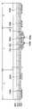
도 1은 종래 유기전계발광표시장치의 단면도이다.1 is a cross-sectional view of a conventional organic light emitting display device.
도 1을 참조하면, 화소영역(Ⅰ)과 비화소영역(Ⅱ)이 구비된 기판(100) 상에 반도체층(110), 게이트 절연막(120), 게이트 전극(130a), 스캔드라이버(130b), 층간 절연막(140) 및 소스/드레인 전극(150)이 구비되고, 소스/드레인 배선으로 이루어진 공통전원공급라인(150b), 제 2 전극 전원공급라인(150a)이 구비된다.Referring to FIG. 1, a
상기 기판(100) 전면에 평탄화막(160)이 구비된다. 상기 평탄화막(160)은 유기물로 아크릴계 수지 또는 폴리이미드계 수지로 이루어진다.The
상기 평탄화막(160)은 상기 공통전원공급라인(150b), 제 2 전극 전원공급라인(150a) 및 소스/드레인 전극(150)을 노출시키는 비어홀들이 구비된다. 상기 공통전원공급라인(150b)을 노출시키는 이유는 추후 기판을 글라스 프릿으로 봉지할 때, 접착력을 좋게 하기 위함이다.The
상기 기판(100) 상에 반사막(170)을 포함하는 제 1 전극(171)이 구비되고, 상기 기판(100) 전면에 화소정의막(180)이 구비된다.The
상기 제 1 전극(171) 상에 적어도 발광층을 포함하는 유기막층(190)이 구비되고, 그 상부에 제 2 전극(200)이 구비된다. 상기 기판(100)에 대향하는 봉지기판(210)이 제공되고, 상기 기판(100)과 봉지기판(210)은 글라스 프릿(220)으로 봉지되어 종래 기술에 따른 유기전계발광표시장치가 구성된다.An
그러나, 종래의 유기전계발광표시장치는 기판을 봉지하는 글라스 프릿의 하부에 소스/드레인 배선인 공통전원공급라인이 위치하게 되는데, 상기 공통전원공급 라인의 폭이 상기 글라스 프릿의 폭보다 넓어서 글라스 프릿에 레이저 조사시, 상기 공통전원공급라인에도 조사되어 레이저의 고열이 상기 제 2 전원공급라인으로 전달되고 이는 제 2 전극을 타고 소자 내부로 전달되어 유기막층이 손상된다. 이로써, 상기 소자의 신뢰성이 저하되는 단점이 있다.However, in the conventional organic light emitting display device, a common power supply line, which is a source / drain line, is positioned under the glass frit encapsulating the substrate. The width of the common power supply line is wider than that of the glass frit. When irradiating the laser, the common power supply line is also irradiated so that high heat of the laser is transmitted to the second power supply line, which is transferred to the inside of the device by the second electrode, thereby damaging the organic layer. As a result, there is a disadvantage in that the reliability of the device is lowered.
따라서, 본 발명은 상기와 같은 종래 기술의 제반단점과 문제점을 해결하기 위한 것으로, 기판을 봉지하는 글라스 프릿에 레이저를 조사하는데 있어서, 상기 레이저의 고열에 의한 소자의 손상을 방지할 수 있는 유기전계발광표시장치 및 그 제조방법을 제공함에 본 발명의 목적이 있다.Accordingly, the present invention is to solve the above-mentioned disadvantages and problems of the prior art, in the irradiation of the laser to the glass frit encapsulating the substrate, an organic electric field that can prevent damage to the device due to the high heat of the laser An object of the present invention is to provide a light emitting display device and a method of manufacturing the same.
본 발명의 상기 목적은 반도체층, 게이트 전극 및 소스/드레인 전극을 포함하는 박막 트랜지스터; 상기 박막 트랜지스터 상에 위치하는 유기평탄화막; 상기 유기평탄화막 상에 위치하는 제 1 전극; 상기 제 1 전극 상에 위치하는 화소정의막; 상기 제 1 전극 및 화소정의막 상에 위치하며, 적어도 발광층을 포함하는 유기막층; 상기 유기막층 상에 위치하는 제 2 전극;을 포함하는 화소영역 및 화소영역 이외의 영역인 비화소영역를 구비하는 기판; 및 상기 기판을 봉지하는 봉지기판을 포함하며, 상기 비화소영역은 메탈 배선; 상기 메탈 배선의 일부분을 노출시키는 개구부를 포함하는 유기평탄화막; 및 상기 개구부 상에 위치하며, 상기 기판과 상 기 봉지기판을 봉지하기 위한 글라스 프릿;을 포함하는 것을 특징으로 하는 유기전계발광표시장치에 의해 달성된다.The object of the present invention is a thin film transistor comprising a semiconductor layer, a gate electrode and a source / drain electrode; An organic planarization layer on the thin film transistor; A first electrode on the organic flattening film; A pixel definition layer positioned on the first electrode; An organic layer disposed on the first electrode and the pixel definition layer and including at least an emission layer; A substrate having a pixel region including and a non-pixel region other than the pixel region; And an encapsulation substrate encapsulating the substrate, wherein the non-pixel region comprises a metal wiring; An organic flattening film including an opening exposing a portion of the metal wiring; And a glass frit positioned on the opening and encapsulating the substrate and the encapsulation substrate.
또한, 본 발명의 상기 목적은 화소영역과 비화소영역을 포함하는 기판을 제공하는 단계; 상기 화소영역의 기판 상에 반도체층, 게이트 전극 및 소스/드레인 전극을 포함하는 박막 트랜지스터 및 상기 비화소영역의 기판 상에 메탈배선을 형성하는 단계; 상기 기판 전면에 유기평탄화막을 형성하는 단계; 상기 비화소영역의 유기평탄화막을 식각하여 상기 메탈배선의 일부영역을 노출시키는 단계; 상기 화소영역의 유기평탄화막 상에 제 1 전극을 형성하는 단계; 상기 기판 전면에 화소정의막을 형성하는 단계; 상기 비화소영역의 메탈배선상의 화소정의막을 식각하는 단계; 상기 화소영역의 제 1 전극 및 화소정의막 상에 적어도 발광층을 포함하는 유기막층을 형성하는 단계; 상기 기판 전면에 제 2 전극을 형성하는 단계; 상기 비화소영역의 메탈배선상의 제 2 전극을 식각하는 단계; 봉지기판을 제공하는 단계; 상기 봉지기판의 외측에 글라스 프릿을 도포하여 상기 기판과 봉지하는 단계;를 포함하는 것을 특징으로 하는 유기전계발광표시장치의 제조방법에 의해 달성된다.In addition, the object of the present invention is to provide a substrate including a pixel region and a non-pixel region; Forming a metal wiring on the substrate of the pixel region and a thin film transistor including a semiconductor layer, a gate electrode, and a source / drain electrode on the substrate of the pixel region; Forming an organic planarization film on the entire surface of the substrate; Etching the organic planarization layer of the non-pixel region to expose a portion of the metal wiring; Forming a first electrode on the organic planarization layer of the pixel region; Forming a pixel defining layer on the entire surface of the substrate; Etching the pixel definition layer on the metallization of the non-pixel region; Forming an organic layer including at least a light emitting layer on the first electrode and the pixel defining layer of the pixel region; Forming a second electrode on the front surface of the substrate; Etching the second electrode on the metal wiring of the non-pixel region; Providing a sealing substrate; And applying a glass frit to the outside of the encapsulation substrate to encapsulate the substrate.
본 발명의 상기 목적과 기술적 구성 및 그에 따른 작용효과에 관한 자세한 사항은 본 발명의 바람직한 실시예를 도시하고 있는 도면을 참조한 이하 상세한 설명에 의해 보다 명확하게 이해될 것이다. 또한 도면들에 있어서, 층 및 영역의 길이, 두께등은 편의를 위하여 과장되어 표현될 수도 있다. 명세서 전체에 걸쳐서 동일한 참조번호들은 동일한 구성요소들을 나타낸다.Details of the above object and technical configuration of the present invention and the effects thereof according to the present invention will be more clearly understood by the following detailed description with reference to the drawings showing preferred embodiments of the present invention. In the drawings, the length, thickness, etc. of layers and regions may be exaggerated for convenience. Like numbers refer to like elements throughout.
도 2 내지 도 5는 본 발명의 실시 예에 따른 유기전계발광표시장치의 단면도 이다.2 to 5 are cross-sectional views of an organic light emitting display device according to an embodiment of the present invention.
도 2을 참조하면, 화소영역(Ⅰ)과 비화소영역(Ⅱ)을 구비하는 기판(300)을 제공한다. 상기 기판(300)은 절연 유리, 플라스틱 또는 도전성 기판을 사용할 수 있다.Referring to FIG. 2, a
이어서, 상기 기판(300) 전면에 버퍼층(310)을 형성한다. 상기 버퍼층(310)은 실리콘 산화막, 실리콘 질화막 또는 이들의 다중층일 수 있다. 또한, 상기 버퍼층(310)은 하부의 기판에서 불순물이 상부로 올라오지 못하도록 방지하는 보호막의 역할을 한다.Subsequently, a
이어서, 상기 화소영역(Ⅰ)의 상기 버퍼층(310) 상에 반도체층(320)을 형성한다. 상기 반도체층(320)은 비정질 실리콘막 또는 이를 결정화한 다결정 실리콘막일 수 있다. 이어 상기 기판(300) 전면에 게이트 절연막(330)을 형성한다. 상기 게이트 절연막(330)은 실리콘 산화막, 실리콘 질화막 또는 이들의 다중층일 수 있다.Subsequently, a
이후에, 상기 게이트 절연막(330) 상에 상기 반도체층(320)의 일부 영역과 대응되게 게이트 전극(340a)을 형성한다. 상기 게이트 전극(340a)은 Al, Cu 또는 Cr을 사용할 수 있다.Thereafter, the
이어서, 상기 기판(300) 전면에 층간 절연막(350)을 형성한다. 상기 층간 절연막(350)은 실리콘산화막, 실리콘질화막 또는 이들의 다중층일 수 있다. 상기 화소영역(Ⅰ) 상의 상기 층간 절연막(350) 및 게이트 절연막(330)을 식각하여 상기 반도체층(320)을 노출시키는 콘택홀(351,352)을 형성한다.Subsequently, an interlayer
이어서, 상기 화소영역(Ⅰ) 상의 층간 절연막(350) 상에 소스/드레인 전극 (360a,360b)을 형성한다. 상기 소스/드레인 전극(360a,360b)은 Mo, Cr, Al, Ti, Au, Pd 또는 Ag로 이루어진 군에서 선택된 하나를 사용할 수 있다. 또한, 상기 소스/드레인 전극(360a,360b)은 상기 콘택홀(351,352)을 통해 상기 반도체층(120)과 연결된다.Subsequently, source /
또한, 상기 소스/드레인 전극(360a,360b)을 형성할 때, 상기 비화소영역(Ⅱ) 상에 메탈 배선(360d)이 동시에 형성되고, 상기 메탈 배선(360d)은 공통전원공급라인으로 작용할 수 있다. 또한, 제 2 전극 전원공급라인(360c)도 형성될 수 있다.In addition, when the source /
또한, 상기 게이트 전극(340a)을 형성할 때, 상기 비화소영역(Ⅱ) 상에 스캔 드라이버(340b)가 동시에 형성될 수 있다.In addition, when the
이때, 상기 소스/드레인 전극(360a,360b) 및 메탈 배선(360d)을 형성할 때, 상기 비화소영역(Ⅱ)에 위치하는 상기 메탈 배선(360d)은 추후 형성되는 글라스 프릿의 폭보다 좁게 형성된다. 일반적으로 상기 글라스 프릿의 폭은 0.7mm정도로 형성되지만, 소자의 규격에 따라 달리지므로 상기 메탈 배선(360d)의 폭의 수치는 한정되지 않고, 상기 글라스 프릿의 폭보다 좁게 형성하는 것이 바람직하다. 이는 추후 기판을 봉지하는 글라스 프릿의 하부에 메탈 배선이 위치하게 되는데, 상기 메탈 배선의 폭이 상기 글라스 프릿의 폭보다 넓으면, 글라스 프릿에 레이저 조사시, 상기 공통전원공급라인으로 작용하는 메탈 배선에도 조사되어 레이저의 고열이 상기 제 2 전극 전원공급라인으로 전달되고 이는 제 2 전극을 타고 소자 내부로 전달되어 유기막층이 손상되는 단점을 방지하기 위함이다.In this case, when the source /
본 발명에서는 탑(top) 게이트 구조의 박막 트랜지스터를 형성하였지만, 이 와는 달리, 게이트 전극이 반도체층 하부에 위치하는 바텀(bottom) 게이트 구조로 형성할 수도 있다.In the present invention, a thin film transistor having a top gate structure is formed, but, alternatively, the gate electrode may be formed as a bottom gate structure under the semiconductor layer.
또한, 본 발명에서는 소스/드레인 전극을 형성할 때, 동시에 메탈 배선을 형성하였지만, 이와는 달리, 게이트 전극 또는 제 1 전극을 형성할 때, 메탈 배선을 동시에 형성할 수도 있다.In the present invention, the metal wirings are formed at the same time when the source / drain electrodes are formed. Alternatively, the metal wirings may be formed simultaneously when the gate electrode or the first electrode is formed.
이어서, 도 3을 참조하면, 상기 기판(300) 전면에 평탄화막(370)을 형성한다. 상기 평탄화막(370)은 유기막 또는 무기막으로 형성하거나 이들의 복합막으로 형성할 수 있다. 상기 평탄화막(370)을 무기막으로 형성하는 경우는 SOG(spin on glass)를 사용하여 형성하는 것이 바람직하고, 유기막으로 형성하는 경우 아크릴계 수지, 폴리이미드계 수지 또는 BCB(benzocyclobutene)을 사용하여 형성하는 것이 바람직하다.3, the
이때, 상기 화소영역(Ⅰ)의 평탄화막(370)을 식각하여 상기 소스/드레인 전극 중 어느 하나를 노출시키는 비어홀(371a)을 형성하고, 상기 비화소영역(Ⅱ)의 평탄화막(370)을 식각하여 상기 메탈 배선(360d)과 상기 제 2 전극 전원공급라인(360c)을 노출시키는 개구부(371b,371c)을 형성한다. 상기 메탈 배선(360d)을 노출시키는 것은 추후 글라스 프릿으로 봉지되었을 때, 기판과의 접착력을 더욱 향상시키기 위함이다.In this case, the
이어서, 도 4를 참조하면, 상기 화소영역(Ⅰ)의 평탄화막(370) 상에 반사막(375)을 포함하는 제 1 전극(380)을 형성한다. 상기 제 1 전극(380)은 상기 비아홀(371)의 바닥에 위치하여 상기 노출된 소스/드레인 전극(360a,360b)중 어느 하나에 접하고, 상기 평탄화막(370) 상으로 연장된다. 상기 제 1 전극(380)은 ITO(Indium Tin Oxide) 또는 IZO(Indium Zinc Oxide)를 사용할 수 있다.4, a
이어서, 상기 제 1 전극(380)을 포함한 기판(300) 전면에 화소정의막(390)을 형성하되, 상기 제 1 전극(380)이 위치한 비아홀(371a)을 충분히 채울 수 있을 정도의 두께로 형성한다. 상기 화소정의막(390)은 유기막 또는 무기막으로 형성할 수 있으나, 바람직하게는 유기막으로 형성한다. 더욱 바람직하게는 상기 화소정의막(390)은 BCB(benzocyclobutene), 아크릴계 고분자 및 폴리이미드로 이루어진 군에서 선택되는 하나이다. 상기 화소정의막은 유동성(flowability)이 뛰어나므로 상기 기판 전체에 평탄하게 형성할 수 있다.Subsequently, the
이때, 상기 화소영역(Ⅰ)의 화소정의막(390)을 식각하여 상기 제 1 전극(380)을 노출시키는 개구부(395a)를 형성하고, 상기 비화소영역(Ⅱ)의 제 2 전극 전원공급라인(360c)를 노출시키는 개구부(395b)를 형성한다.In this case, the
또한, 상기 비화소영역(Ⅱ)의 메탈 배선(360d) 상부에도 상기 화소정의막(390)이 존재하지 않도록 식각한다.In addition, the
이어서, 상기 개구부(395)를 통해 노출된 제 1 전극(380) 상에 유기막층(400)을 형성한다. 상기 유기막층(400)은 적어도 발광층을 포함하며, 정공주입층, 정공수송층, 전자수송층 또는 전자주입층중 어느 하나 이상의 층을 추가로 포함할 수 있다.Subsequently, the
이어서, 상기 기판(300) 전면에 제 2 전극(410)을 형성한다. 상기 제 2 전극(410)은 투과전극으로 투명하면서 일함수가 낮은 Mg, Ag, Al, Ca 및 이들의 합금으 로 사용할 수 있다. 이때, 상기 비화소영역(Ⅱ)의 제 2 전극(410)을 식각하여 상기 메탈 배선(360d) 및 평탄화막(370)을 노출시킨다.Subsequently, a
다음에, 도 5를 참조하면, 상기 기판(300)에 대향하는 봉지기판(420)을 제공한다. 상기 봉지기판(420)은 에칭된 절연유리 또는 에칭되지 않은 절연유리를 사용할 수 있다.Next, referring to FIG. 5, an
이어서, 상기 봉지기판(420)의 외측에 글라스 프릿(430)을 형성한다. 즉 기판에 대향하는 봉지기판 외측에 글라스 프릿(430)을 도포한다.Subsequently, a
상기 글라스 프릿(430)은 산화납(PbO), 삼산화이붕소(B2O8) 및 이산화규소(SiO2)로 이루어진 군에서 선택된 하나를 사용할 수 있으며, 디스펜싱(dispensing)법 또는 스크린 인쇄법을 사용하여 도포할 수 있다.The
본 실시 예에서는 상기 봉지기판(420) 상에 글라스 프릿(430)을 형성하였지만, 상기 기판(300) 상에 형성할 수도 있다.Although the
이어서, 상기 기판(300)과 봉지기판(420)을 얼라인한 후, 합착한다. 이때, 상기 글라스 프릿(430)은 상기 기판(300) 상의 메탈 배선(360d) 및 평탄화막(370)에 접촉하게 된다.Subsequently, the
다음에, 상기 글라스 프릿(430)에 레이저를 조사하여 상기 글라스 프릿(430)을 용융하고, 고상화하여 상기 기판 및 봉지기판에 접착되도록 하여 본 발명의 유기전계발광표시장치를 완성한다.Next, the
상기와 같이, 기판 외측에 위치하며, 추후 글라스 프릿과 접촉하는 메탈 배선의 폭을 상기 글라스 프릿의 폭보다 좁게 형성하여, 종래 상기 글라스 프릿에 레 이저를 조사할 때, 열이 소자 내부로 전달되어 소자의 신뢰성을 저하시키는 단점을 방지할 수 있는 이점이 있다.As described above, when the width of the metal wiring positioned outside the substrate and in contact with the glass frit is formed to be smaller than the width of the glass frit, heat is transferred into the device when the laser is irradiated to the glass frit. There is an advantage that can prevent the disadvantage of lowering the reliability of the device.
본 발명은 이상에서 살펴본 바와 같이 바람직한 실시예를 들어 도시하고 설명하였으나, 상기한 실시 예에 한정되지 아니하며 본 발명의 정신을 벗어나지 않는 범위 내에서 당해 발명이 속하는 기술분야에서 통상의 지식을 가진 자에 의해 다양한 변경과 수정이 가능할 것이다.The present invention has been shown and described with reference to the preferred embodiments as described above, but is not limited to the above embodiments and those skilled in the art without departing from the spirit of the present invention. Various changes and modifications will be possible.
따라서, 본 발명의 유기전계발광표시장치 및 그 제조방법은 기판을 봉지하는 글라스 프릿에 레이저를 조사하는데 있어서, 상기 레이저의 고열에 의한 소자의 손상을 방지할 수 있는 효과가 있다.Therefore, the organic light emitting display device and the manufacturing method thereof according to the present invention have an effect of preventing damage to the device due to the high heat of the laser when irradiating the laser to the glass frit encapsulating the substrate.
Claims (12)
Translated fromKoreanPriority Applications (7)
| Application Number | Priority Date | Filing Date | Title |
|---|---|---|---|
| KR1020060007025AKR100635514B1 (en) | 2006-01-23 | 2006-01-23 | Organic light emitting display device and manufacturing method |
| JP2006189628AJP4472668B2 (en) | 2006-01-23 | 2006-07-10 | Organic electroluminescent display device and manufacturing method thereof |
| US11/529,916US8120249B2 (en) | 2006-01-23 | 2006-09-29 | Organic light emitting display and method of fabricating the same |
| TW095142899ATWI341144B (en) | 2006-01-23 | 2006-11-20 | Organic light emitting display and method of fabricating the same |
| CN2007100040808ACN101009311B (en) | 2006-01-23 | 2007-01-23 | Organic light emitting display and method of fabricating the same |
| EP07250270.1AEP1811571B1 (en) | 2006-01-23 | 2007-01-23 | Organic light emitting display and method of fabricating the same |
| EP07250267.7AEP1811570B1 (en) | 2006-01-23 | 2007-01-23 | Organic light emitting display and method of fabricating the same |
Applications Claiming Priority (1)
| Application Number | Priority Date | Filing Date | Title |
|---|---|---|---|
| KR1020060007025AKR100635514B1 (en) | 2006-01-23 | 2006-01-23 | Organic light emitting display device and manufacturing method |
Publications (1)
| Publication Number | Publication Date |
|---|---|
| KR100635514B1true KR100635514B1 (en) | 2006-10-18 |
Family
ID=37626512
Family Applications (1)
| Application Number | Title | Priority Date | Filing Date |
|---|---|---|---|
| KR1020060007025AActiveKR100635514B1 (en) | 2006-01-23 | 2006-01-23 | Organic light emitting display device and manufacturing method |
Country Status (6)
| Country | Link |
|---|---|
| US (1) | US8120249B2 (en) |
| EP (1) | EP1811571B1 (en) |
| JP (1) | JP4472668B2 (en) |
| KR (1) | KR100635514B1 (en) |
| CN (1) | CN101009311B (en) |
| TW (1) | TWI341144B (en) |
Cited By (8)
| Publication number | Priority date | Publication date | Assignee | Title |
|---|---|---|---|---|
| US7777225B2 (en) | 2007-05-21 | 2010-08-17 | Samsung Mobile Display Co., Ltd. | Organic light-emitting display device |
| US7876038B2 (en) | 2008-02-04 | 2011-01-25 | Samsung Mobile Display Co., Ltd. | Organic light emitting display |
| US7915101B2 (en) | 2007-05-10 | 2011-03-29 | Samsung Mobile Display Co., Ltd. | Thin film transistor and organic light emitting display using the same |
| KR20150049141A (en)* | 2013-10-29 | 2015-05-08 | 삼성디스플레이 주식회사 | Organic light emitting display devices and methods of manufacturing organic light emitting display devices |
| US9362531B2 (en) | 2013-10-14 | 2016-06-07 | Samsung Display Co., Ltd. | Organic light emitting display device and manufacturing method thereof |
| US9502683B2 (en) | 2014-06-24 | 2016-11-22 | Samsung Display Co., Ltd. | Sealing portion structure for display device |
| KR20160136517A (en)* | 2015-05-19 | 2016-11-30 | 삼성디스플레이 주식회사 | Organic light-emitting display apparatus and manufacturing the same |
| KR20190030951A (en)* | 2017-09-15 | 2019-03-25 | 엘지디스플레이 주식회사 | Display device |
Families Citing this family (74)
| Publication number | Priority date | Publication date | Assignee | Title |
|---|---|---|---|---|
| US7928654B2 (en)* | 2003-08-29 | 2011-04-19 | Semiconductor Energy Laboratory Co., Ltd. | Display device and method for manufacturing the same |
| US20070108900A1 (en)* | 2005-11-15 | 2007-05-17 | Boek Heather D | Method and apparatus for the elimination of interference fringes in an OLED device |
| US7425166B2 (en)* | 2005-12-06 | 2008-09-16 | Corning Incorporated | Method of sealing glass substrates |
| US7597603B2 (en)* | 2005-12-06 | 2009-10-06 | Corning Incorporated | Method of encapsulating a display element |
| US7537504B2 (en)* | 2005-12-06 | 2009-05-26 | Corning Incorporated | Method of encapsulating a display element with frit wall and laser beam |
| US8038495B2 (en) | 2006-01-20 | 2011-10-18 | Samsung Mobile Display Co., Ltd. | Organic light-emitting display device and manufacturing method of the same |
| KR100673765B1 (en) | 2006-01-20 | 2007-01-24 | 삼성에스디아이 주식회사 | Organic light emitting display device and manufacturing method |
| JP4624309B2 (en)* | 2006-01-24 | 2011-02-02 | 三星モバイルディスプレイ株式會社 | Organic electroluminescent display device and manufacturing method thereof |
| JP4456092B2 (en)* | 2006-01-24 | 2010-04-28 | 三星モバイルディスプレイ株式會社 | Organic electroluminescent display device and manufacturing method thereof |
| KR100671641B1 (en) | 2006-01-25 | 2007-01-19 | 삼성에스디아이 주식회사 | Organic electroluminescent display and manufacturing method thereof |
| KR100685853B1 (en)* | 2006-01-25 | 2007-02-22 | 삼성에스디아이 주식회사 | Organic light emitting display device and manufacturing method |
| KR100688796B1 (en)* | 2006-01-25 | 2007-03-02 | 삼성에스디아이 주식회사 | Organic light emitting display device and manufacturing method thereof |
| US8164257B2 (en)* | 2006-01-25 | 2012-04-24 | Samsung Mobile Display Co., Ltd. | Organic light emitting display and method of fabricating the same |
| KR100688795B1 (en)* | 2006-01-25 | 2007-03-02 | 삼성에스디아이 주식회사 | Organic light emitting display device and manufacturing method |
| KR100732808B1 (en)* | 2006-01-26 | 2007-06-27 | 삼성에스디아이 주식회사 | Manufacturing method of organic light emitting display device |
| JP4633674B2 (en) | 2006-01-26 | 2011-02-16 | 三星モバイルディスプレイ株式會社 | Organic electroluminescent display device and manufacturing method thereof |
| KR100671647B1 (en)* | 2006-01-26 | 2007-01-19 | 삼성에스디아이 주식회사 | Organic light emitting display device |
| KR100759666B1 (en)* | 2006-01-27 | 2007-09-17 | 삼성에스디아이 주식회사 | Flat panel display and manufacturing method thereof |
| KR100671639B1 (en)* | 2006-01-27 | 2007-01-19 | 삼성에스디아이 주식회사 | Organic electroluminescent display and manufacturing method thereof |
| KR100688792B1 (en)* | 2006-01-27 | 2007-03-02 | 삼성에스디아이 주식회사 | Flat panel display and manufacturing method thereof |
| KR100688790B1 (en)* | 2006-01-27 | 2007-03-02 | 삼성에스디아이 주식회사 | Organic electroluminescent display and manufacturing method thereof |
| US20070188757A1 (en)* | 2006-02-14 | 2007-08-16 | Jeffrey Michael Amsden | Method of sealing a glass envelope |
| KR100732817B1 (en) | 2006-03-29 | 2007-06-27 | 삼성에스디아이 주식회사 | Organic light emitting display device and manufacturing method |
| US20070267972A1 (en)* | 2006-05-22 | 2007-11-22 | Menegus Harry E | Method for forming a temporary hermetic seal for an OLED display device |
| US20080124558A1 (en)* | 2006-08-18 | 2008-05-29 | Heather Debra Boek | Boro-silicate glass frits for hermetic sealing of light emitting device displays |
| US20080049431A1 (en)* | 2006-08-24 | 2008-02-28 | Heather Debra Boek | Light emitting device including anti-reflection layer(s) |
| US20080048556A1 (en)* | 2006-08-24 | 2008-02-28 | Stephan Lvovich Logunov | Method for hermetically sealing an OLED display |
| US7800303B2 (en)* | 2006-11-07 | 2010-09-21 | Corning Incorporated | Seal for light emitting display device, method, and apparatus |
| US20080168801A1 (en)* | 2007-01-12 | 2008-07-17 | Paul Stephen Danielson | Method of sealing glass |
| US20080200088A1 (en)* | 2007-02-21 | 2008-08-21 | Chong Pyung An | Method for reducing interference fringes in a display device |
| US7652305B2 (en)* | 2007-02-23 | 2010-01-26 | Corning Incorporated | Methods and apparatus to improve frit-sealed glass package |
| US20080213482A1 (en)* | 2007-03-01 | 2008-09-04 | Stephan Lvovich Logunov | Method of making a mask for sealing a glass package |
| US20090044496A1 (en)* | 2007-08-16 | 2009-02-19 | Botelho John W | Method and apparatus for sealing a glass package |
| US8147632B2 (en)* | 2008-05-30 | 2012-04-03 | Corning Incorporated | Controlled atmosphere when sintering a frit to a glass plate |
| US7992411B2 (en) | 2008-05-30 | 2011-08-09 | Corning Incorporated | Method for sintering a frit to a glass plate |
| US8448468B2 (en) | 2008-06-11 | 2013-05-28 | Corning Incorporated | Mask and method for sealing a glass envelope |
| US20100095705A1 (en) | 2008-10-20 | 2010-04-22 | Burkhalter Robert S | Method for forming a dry glass-based frit |
| KR101002659B1 (en)* | 2008-12-23 | 2010-12-20 | 삼성모바일디스플레이주식회사 | Organic light emitting display |
| JP5240718B2 (en)* | 2009-02-20 | 2013-07-17 | パナソニック株式会社 | Organic EL module |
| KR101084230B1 (en)* | 2009-11-16 | 2011-11-16 | 삼성모바일디스플레이주식회사 | Organic light emitting display device and manufacturing method of organic light emitting display device |
| WO2011108115A1 (en) | 2010-03-05 | 2011-09-09 | ヤマト電子株式会社 | Lead-free glass material for organic-el sealing, organic el display formed using same, and process for producing the display |
| CN101847652B (en)* | 2010-04-21 | 2011-08-17 | 友达光电股份有限公司 | Electroluminescent display panel |
| KR101234228B1 (en)* | 2010-06-04 | 2013-02-18 | 삼성디스플레이 주식회사 | Organic light emitting display apparatus |
| KR101827551B1 (en)* | 2010-10-15 | 2018-03-23 | 삼성디스플레이 주식회사 | Organic light emitting diode display and method for fabricating of the same |
| TWI743509B (en) | 2011-05-05 | 2021-10-21 | 日商半導體能源研究所股份有限公司 | Semiconductor device and method for manufacturing the same |
| WO2013031509A1 (en)* | 2011-08-26 | 2013-03-07 | Semiconductor Energy Laboratory Co., Ltd. | Light-emitting device, electronic device, lighting device, and method for manufacturing the light-emitting device |
| CN102709480B (en)* | 2011-11-25 | 2016-01-27 | 京东方科技集团股份有限公司 | Organic electroluminescence device and display |
| KR102058387B1 (en)* | 2011-11-28 | 2019-12-24 | 가부시키가이샤 한도오따이 에네루기 켄큐쇼 | Glass pattern and method for forming the same, sealed body and method for manufacturing the same, and light-emitting device |
| TWI570906B (en) | 2011-11-29 | 2017-02-11 | 半導體能源研究所股份有限公司 | Sealing structure, illuminating device, electronic device, and lighting device |
| KR102001815B1 (en) | 2011-11-29 | 2019-07-19 | 가부시키가이샤 한도오따이 에네루기 켄큐쇼 | Method of manufacturing sealed body and method of manufacturing light-emitting device |
| KR20140016170A (en)* | 2012-07-30 | 2014-02-07 | 가부시키가이샤 한도오따이 에네루기 켄큐쇼 | Sealing structure and organic electroluminescence device |
| WO2014035954A2 (en) | 2012-08-30 | 2014-03-06 | Corning Incorporated | Antimony-free glass, antimony-free frit and a glass package that is hermetically sealed with the frit |
| DE102012109258B4 (en)* | 2012-09-28 | 2020-02-06 | Osram Oled Gmbh | Optoelectronic component and method for producing an optoelectronic component |
| KR101993331B1 (en)* | 2013-01-03 | 2019-06-27 | 삼성디스플레이 주식회사 | Organinc light emitting display device and manufacturing method for the same |
| CN103943649B (en)* | 2013-02-15 | 2017-10-03 | 上海天马微电子有限公司 | Oled display panel and driving method thereof |
| KR20150071318A (en)* | 2013-12-18 | 2015-06-26 | 삼성디스플레이 주식회사 | Method for manufaturing of organic light emitting diode display |
| KR102360783B1 (en)* | 2014-09-16 | 2022-02-10 | 삼성디스플레이 주식회사 | display device |
| CN104538566A (en)* | 2015-01-22 | 2015-04-22 | 深圳市华星光电技术有限公司 | Packaging method of OLED (Organic Light Emitting Diode) and OLED packaging structure |
| CN104617007B (en)* | 2015-01-23 | 2017-08-01 | 京东方科技集团股份有限公司 | Method for Improving the Accuracy of Encapsulation Graphic Sealing Test, Motherboard and Mask Board |
| CN104795425A (en) | 2015-03-30 | 2015-07-22 | 京东方科技集团股份有限公司 | Organic light emitting diode touch display screen and manufacturing method thereof |
| KR102483950B1 (en)* | 2015-04-28 | 2023-01-03 | 삼성디스플레이 주식회사 | Material for sealing display apparatus, organic light-emitting display apparatus comprising the same, and method for manufacturing organic light-emitting display apparatus |
| CN105739154B (en) | 2016-04-29 | 2019-09-27 | 上海天马有机发光显示技术有限公司 | A display panel and electronic device |
| KR102610710B1 (en)* | 2016-06-10 | 2023-12-08 | 삼성디스플레이 주식회사 | Display device and fabricating method thereof |
| CN107046104A (en)* | 2017-01-10 | 2017-08-15 | 广东欧珀移动通信有限公司 | OLED encapsulation structure and preparation method thereof |
| CN109390352A (en)* | 2017-08-09 | 2019-02-26 | 昆山国显光电有限公司 | Array substrate and its manufacturing method, display panel and its manufacturing method |
| CN111758300B (en)* | 2018-02-26 | 2023-08-29 | 夏普株式会社 | Display device and method for manufacturing the same |
| KR102663522B1 (en)* | 2018-11-05 | 2024-05-16 | 삼성디스플레이 주식회사 | Display device and method for manufacturing of the same |
| CN109728195B (en)* | 2018-12-29 | 2021-05-18 | 厦门天马微电子有限公司 | Display panel and display device |
| KR102763278B1 (en)* | 2019-12-31 | 2025-02-10 | 삼성디스플레이 주식회사 | Display panel |
| TWI729862B (en) | 2020-06-22 | 2021-06-01 | 友達光電股份有限公司 | Organic light emitting panel and fabrication method thereof |
| CN111732342B (en)* | 2020-08-07 | 2022-12-27 | 上海银浆科技有限公司 | Glass component and crystalline silicon solar cell conductive silver paste containing same |
| KR20220058687A (en) | 2020-10-29 | 2022-05-10 | 삼성디스플레이 주식회사 | Display device |
| CN113387601A (en)* | 2021-05-31 | 2021-09-14 | 西南电子技术研究所(中国电子科技集团公司第十研究所) | Method for improving glass welding strength with assistance of high-vacuum magnetron sputtering interface |
| WO2023019531A1 (en)* | 2021-08-19 | 2023-02-23 | 京东方科技集团股份有限公司 | Display device, and display panel and manufacturing method therefor |
Citations (1)
| Publication number | Priority date | Publication date | Assignee | Title |
|---|---|---|---|---|
| JPH11329717A (en) | 1998-05-15 | 1999-11-30 | Sharp Corp | Color EL panel |
Family Cites Families (180)
| Publication number | Priority date | Publication date | Assignee | Title |
|---|---|---|---|---|
| US3966449A (en)* | 1975-02-10 | 1976-06-29 | International Business Machines Corporation | Sealing glass composition and process |
| US4105292A (en)* | 1975-09-02 | 1978-08-08 | Minnesota Mining And Manufacturing Company | Optical element to assure a minimum spacing |
| US4004936A (en)* | 1976-05-19 | 1977-01-25 | International Business Machines Corporation | Low temperature sealed glass compositions and process for their preparation |
| US4238704A (en)* | 1979-02-12 | 1980-12-09 | Corning Glass Works | Sealed beam lamp of borosilicate glass with a sealing glass of zinc silicoborate and a mill addition of cordierite |
| JPS5966157A (en)* | 1982-10-08 | 1984-04-14 | Fujitsu Ltd | Semiconductor device and its manufacturing method |
| JPS60216333A (en)* | 1984-04-12 | 1985-10-29 | Asahi Glass Co Ltd | Electrochromic display element |
| JPH0682765B2 (en)* | 1985-12-25 | 1994-10-19 | 株式会社日立製作所 | Liquid crystal display element |
| US6980275B1 (en) | 1993-09-20 | 2005-12-27 | Semiconductor Energy Laboratory Co., Ltd. | Electro-optical device |
| JP3135793B2 (en)* | 1994-09-02 | 2001-02-19 | シャープ株式会社 | Liquid crystal display device and manufacturing method thereof |
| US6195142B1 (en)* | 1995-12-28 | 2001-02-27 | Matsushita Electrical Industrial Company, Ltd. | Organic electroluminescence element, its manufacturing method, and display device using organic electroluminescence element |
| US5811927A (en)* | 1996-06-21 | 1998-09-22 | Motorola, Inc. | Method for affixing spacers within a flat panel display |
| JPH1074583A (en)* | 1996-08-30 | 1998-03-17 | Sanyo Electric Co Ltd | Organic EL display and method of manufacturing organic EL display |
| US6109994A (en)* | 1996-12-12 | 2000-08-29 | Candescent Technologies Corporation | Gap jumping to seal structure, typically using combination of vacuum and non-vacuum environments |
| JPH10270592A (en)* | 1997-03-24 | 1998-10-09 | Texas Instr Japan Ltd | Semiconductor device and manufacturing method thereof |
| JP3169864B2 (en) | 1997-09-18 | 2001-05-28 | 日本電気株式会社 | LCD panel manufacturing equipment |
| US5965907A (en) | 1997-09-29 | 1999-10-12 | Motorola, Inc. | Full color organic light emitting backlight device for liquid crystal display applications |
| JP3024609B2 (en)* | 1997-10-09 | 2000-03-21 | 日本電気株式会社 | Liquid crystal display cell sealing device |
| JP2845239B1 (en)* | 1997-12-17 | 1999-01-13 | 日本電気株式会社 | Organic thin film EL device and manufacturing method thereof |
| JP3912711B2 (en)* | 1998-11-27 | 2007-05-09 | ローム株式会社 | Organic EL device |
| JP3517624B2 (en)* | 1999-03-05 | 2004-04-12 | キヤノン株式会社 | Image forming device |
| JP2000268969A (en) | 1999-03-17 | 2000-09-29 | Tdk Corp | Organic electroluminescent element |
| JP2000306664A (en) | 1999-04-21 | 2000-11-02 | Stanley Electric Co Ltd | Organic EL display |
| TWI240592B (en) | 1999-06-03 | 2005-09-21 | Koninkl Philips Electronics Nv | Organic electroluminescent device |
| JP2001022293A (en) | 1999-07-07 | 2001-01-26 | Sony Corp | Planar display element |
| JP2001052858A (en) | 1999-08-05 | 2001-02-23 | Futaba Corp | Organic el display device |
| US6452323B1 (en) | 1999-09-20 | 2002-09-17 | Omnion Technologies, Inc. | Luminous gas discharge display having dielectric sealing layer |
| JP3942770B2 (en) | 1999-09-22 | 2007-07-11 | 株式会社半導体エネルギー研究所 | EL display device and electronic device |
| JP4345153B2 (en) | 1999-09-27 | 2009-10-14 | ソニー株式会社 | Manufacturing method of video display device |
| US6833668B1 (en) | 1999-09-29 | 2004-12-21 | Sanyo Electric Co., Ltd. | Electroluminescence display device having a desiccant |
| JP3423261B2 (en)* | 1999-09-29 | 2003-07-07 | 三洋電機株式会社 | Display device |
| JP2001110564A (en) | 1999-10-07 | 2001-04-20 | Gunze Ltd | Electroluminescence lamp |
| KR100480146B1 (en)* | 1999-10-30 | 2005-04-06 | 엘지.필립스 엘시디 주식회사 | Apparatus and Method of Fabricating Liquid Crystal Display Device |
| US7112115B1 (en) | 1999-11-09 | 2006-09-26 | Semiconductor Energy Laboratory Co., Ltd. | Light emitting device and method of manufacturing the same |
| JP3409764B2 (en) | 1999-12-28 | 2003-05-26 | 日本電気株式会社 | Manufacturing method of organic EL display panel |
| US6515417B1 (en) | 2000-01-27 | 2003-02-04 | General Electric Company | Organic light emitting device and method for mounting |
| US6555025B1 (en)* | 2000-01-31 | 2003-04-29 | Candescent Technologies Corporation | Tuned sealing material for sealing of a flat panel display |
| CN1227751C (en)* | 2000-02-17 | 2005-11-16 | Lg电子株式会社 | Organic electroluminescent display panel and packaging method thereof |
| JP2001230072A (en) | 2000-02-18 | 2001-08-24 | Denso Corp | Organic el display device |
| US6650392B2 (en)* | 2000-03-15 | 2003-11-18 | Kabushiki Kaisha Toshiba | Cell structure of liquid crystal device |
| JP2001307633A (en) | 2000-04-20 | 2001-11-02 | Mitsubishi Electric Corp | Flat display panel, flat display device, and method of manufacturing flat display panel |
| US7579203B2 (en)* | 2000-04-25 | 2009-08-25 | Semiconductor Energy Laboratory Co., Ltd. | Light emitting device |
| JP2001319775A (en) | 2000-05-10 | 2001-11-16 | Auto Network Gijutsu Kenkyusho:Kk | Sealing method and sealing structure for organic EL display device |
| JP2001324662A (en) | 2000-05-16 | 2001-11-22 | Ricoh Co Ltd | Lens interlocking mechanism |
| JP2002020169A (en) | 2000-07-03 | 2002-01-23 | Murata Mfg Co Ltd | High-frequecy dielectric porcelain composition, dielectric resonator, dielectric filter, dielectric duplexer and communications equipment |
| JP4889883B2 (en) | 2000-07-10 | 2012-03-07 | 株式会社半導体エネルギー研究所 | Film forming method and film forming apparatus |
| US6956324B2 (en) | 2000-08-04 | 2005-10-18 | Semiconductor Energy Laboratory Co., Ltd. | Semiconductor device and manufacturing method therefor |
| US6605826B2 (en)* | 2000-08-18 | 2003-08-12 | Semiconductor Energy Laboratory Co., Ltd. | Light-emitting device and display device |
| US7255823B1 (en) | 2000-09-06 | 2007-08-14 | Institute Of Materials Research And Engineering | Encapsulation for oled devices |
| JP2002169135A (en) | 2000-09-07 | 2002-06-14 | Seiko Epson Corp | Cell gap adjusting device, pressure sealing device, and liquid crystal display device manufacturing method |
| JP4801297B2 (en) | 2000-09-08 | 2011-10-26 | 株式会社半導体エネルギー研究所 | Light emitting device |
| US6924594B2 (en) | 2000-10-03 | 2005-08-02 | Semiconductor Energy Laboratory Co., Ltd. | Light emitting device |
| JP2002117777A (en) | 2000-10-11 | 2002-04-19 | Matsushita Electric Ind Co Ltd | Gas discharge panel and its manufacturing method |
| JP4223211B2 (en) | 2000-11-14 | 2009-02-12 | 株式会社半導体エネルギー研究所 | Method for manufacturing light emitting device |
| US7178927B2 (en) | 2000-11-14 | 2007-02-20 | Semiconductor Energy Laboratory Co., Ltd. | Electroluminescent device having drying agent |
| JP2002170664A (en) | 2000-12-05 | 2002-06-14 | Toray Ind Inc | Organic electroluminescent device |
| US6646284B2 (en)* | 2000-12-12 | 2003-11-11 | Semiconductor Energy Laboratory Co., Ltd. | Light emitting device and method of manufacturing the same |
| MY145695A (en) | 2001-01-24 | 2012-03-30 | Nichia Corp | Light emitting diode, optical semiconductor device, epoxy resin composition suited for optical semiconductor device, and method for manufacturing the same |
| US6554672B2 (en)* | 2001-03-12 | 2003-04-29 | Micron Technology, Inc. | Flat panel display, method of high vacuum sealing |
| JP2002280169A (en) | 2001-03-19 | 2002-09-27 | Futaba Corp | Organic EL device |
| TWI222838B (en) | 2001-04-10 | 2004-10-21 | Chi Mei Optoelectronics Corp | Packaging method of organic electroluminescence light-emitting display device |
| JP2002318547A (en) | 2001-04-24 | 2002-10-31 | Sony Corp | Method of manufacturing display panel |
| US6424009B1 (en) | 2001-05-04 | 2002-07-23 | Advanced Micro Devices, Inc. | Polysilicon insulator material in semiconductor-on-insulator (SOI) structure |
| WO2003005774A1 (en) | 2001-05-24 | 2003-01-16 | Orion Electric Co., Ltd. | Container for encapsulating oled and manufacturing method thereof |
| JP2002359070A (en) | 2001-05-31 | 2002-12-13 | Matsushita Electric Ind Co Ltd | Organic light emitting device and display panel using the same |
| US6565400B1 (en) | 2001-06-26 | 2003-05-20 | Candescent Technologies Corporation | Frit protection in sealing process for flat panel displays |
| US6660547B2 (en)* | 2001-07-26 | 2003-12-09 | Osram Opto Semiconductors Gmbh | Stabilization for thin substrates |
| JP2003068472A (en) | 2001-08-29 | 2003-03-07 | Hitachi Ltd | Organic light emitting device and organic light emitting display using the same |
| TW517356B (en)* | 2001-10-09 | 2003-01-11 | Delta Optoelectronics Inc | Package structure of display device and its packaging method |
| US20030077396A1 (en) | 2001-10-23 | 2003-04-24 | Lecompte Robert S. | Dip coating system |
| KR100865284B1 (en)* | 2001-10-31 | 2008-10-27 | 엘지디스플레이 주식회사 | Sealing structure of liquid crystal panel |
| TW564563B (en) | 2001-11-29 | 2003-12-01 | Highlink Technology Corp | Light-emitting device with increased stability |
| KR100819864B1 (en)* | 2001-12-28 | 2008-04-07 | 엘지.필립스 엘시디 주식회사 | Organic electroluminescent device |
| TW515062B (en) | 2001-12-28 | 2002-12-21 | Delta Optoelectronics Inc | Package structure with multiple glue layers |
| US7038377B2 (en) | 2002-01-16 | 2006-05-02 | Seiko Epson Corporation | Display device with a narrow frame |
| CN1212662C (en) | 2002-01-16 | 2005-07-27 | 翰立光电股份有限公司 | Package structure of display components |
| JP2003216059A (en) | 2002-01-24 | 2003-07-30 | Sharp Corp | Indicating element and method of manufacturing the same |
| JP2003228302A (en) | 2002-02-04 | 2003-08-15 | Toshiba Electronic Engineering Corp | Display device and method of manufacturing the same |
| JP4069639B2 (en) | 2002-02-12 | 2008-04-02 | セイコーエプソン株式会社 | Manufacturing method of electro-optical device |
| US6791660B1 (en) | 2002-02-12 | 2004-09-14 | Seiko Epson Corporation | Method for manufacturing electrooptical device and apparatus for manufacturing the same, electrooptical device and electronic appliances |
| KR100720414B1 (en) | 2002-02-27 | 2007-05-22 | 엘지.필립스 엘시디 주식회사 | Manufacturing Method Of Liquid Crystal Display |
| JP3875130B2 (en) | 2002-03-26 | 2007-01-31 | 株式会社東芝 | Display device and manufacturing method thereof |
| JP2003297552A (en) | 2002-03-29 | 2003-10-17 | Pioneer Electronic Corp | Organic electroluminescence display panel |
| GB0208143D0 (en)* | 2002-04-09 | 2002-05-22 | Ibm | Data recovery system |
| KR100563675B1 (en)* | 2002-04-09 | 2006-03-28 | 캐논 가부시끼가이샤 | Organic light emitting device and organic light emitting device package |
| DE10219951A1 (en) | 2002-05-03 | 2003-11-13 | Patent Treuhand Ges Fuer Elektrische Gluehlampen Mbh | Process for encapsulating a component based on organic semiconductors |
| US7423375B2 (en) | 2002-05-07 | 2008-09-09 | Osram Gmbh | Encapsulation for electroluminescent devices |
| TWI263339B (en)* | 2002-05-15 | 2006-10-01 | Semiconductor Energy Lab | Light emitting device and method for manufacturing the same |
| KR100477745B1 (en) | 2002-05-23 | 2005-03-18 | 삼성에스디아이 주식회사 | Encapsulation method of organic electro luminescence device and organic electro luminescence panel using the same |
| KR100434408B1 (en)* | 2002-05-29 | 2004-06-04 | 엘지.필립스디스플레이(주) | Element for color flat-type displays |
| JP2004014332A (en) | 2002-06-07 | 2004-01-15 | Pioneer Electronic Corp | Flat display panel and its manufacturing method |
| JP4454262B2 (en) | 2002-07-25 | 2010-04-21 | 三洋電機株式会社 | Electroluminescence display device |
| US7193364B2 (en) | 2002-09-12 | 2007-03-20 | Osram Opto Semiconductors (Malaysia) Sdn. Bhd | Encapsulation for organic devices |
| JP4261861B2 (en) | 2002-09-30 | 2009-04-30 | 双葉電子工業株式会社 | Sealing material for fluorescent display tube and fluorescent display tube |
| JP4050972B2 (en) | 2002-10-16 | 2008-02-20 | 株式会社 日立ディスプレイズ | Display device |
| JP2004171968A (en) | 2002-11-21 | 2004-06-17 | Hitachi Ltd | Flat panel display |
| JP4467879B2 (en) | 2002-11-22 | 2010-05-26 | 株式会社フジクラ | Manufacturing method of dye-sensitized solar cell |
| JP4711595B2 (en) | 2002-12-10 | 2011-06-29 | 株式会社半導体エネルギー研究所 | EL display and electronic device |
| KR100641793B1 (en) | 2002-12-26 | 2006-11-02 | 샤프 가부시키가이샤 | Display panel and method for fabricating the same |
| KR100497095B1 (en) | 2002-12-26 | 2005-06-28 | 엘지.필립스 엘시디 주식회사 | Array substrate for dual panel type electroluminescent device and method for fabricating the same |
| JP4299021B2 (en) | 2003-02-19 | 2009-07-22 | ヤマト電子株式会社 | Sealing material and sealing paste |
| JP3975944B2 (en) | 2003-02-27 | 2007-09-12 | 住友電気工業株式会社 | HOLDER FOR SEMICONDUCTOR OR LIQUID CRYSTAL MANUFACTURING DEVICE AND SEMICONDUCTOR OR LIQUID CRYSTAL MANUFACTURING DEVICE WITH THE SAME |
| JP2004303733A (en) | 2003-03-31 | 2004-10-28 | Osram Opto Semiconductors Gmbh | Display device with components, especially organic light-emitting diodes |
| US7202602B2 (en)* | 2003-04-08 | 2007-04-10 | Organic Lighting Technologies Llc | Metal seal packaging for organic light emitting diode device |
| JP4346012B2 (en) | 2003-04-11 | 2009-10-14 | 大日本印刷株式会社 | Organic electroluminescence device |
| US7098589B2 (en) | 2003-04-15 | 2006-08-29 | Luminus Devices, Inc. | Light emitting devices with high light collimation |
| US7344901B2 (en) | 2003-04-16 | 2008-03-18 | Corning Incorporated | Hermetically sealed package and method of fabricating of a hermetically sealed package |
| US6998776B2 (en)* | 2003-04-16 | 2006-02-14 | Corning Incorporated | Glass package that is hermetically sealed with a frit and method of fabrication |
| US20040206953A1 (en) | 2003-04-16 | 2004-10-21 | Robert Morena | Hermetically sealed glass package and method of fabrication |
| JP4518747B2 (en) | 2003-05-08 | 2010-08-04 | 三洋電機株式会社 | Organic EL display device |
| JP2004342336A (en) | 2003-05-13 | 2004-12-02 | Semiconductor Energy Lab Co Ltd | Light emitting device and manufacturing method thereof |
| KR100560510B1 (en)* | 2003-06-10 | 2006-03-14 | 삼성에스디아이 주식회사 | Plasma display panel |
| US7247986B2 (en)* | 2003-06-10 | 2007-07-24 | Samsung Sdi. Co., Ltd. | Organic electro luminescent display and method for fabricating the same |
| AU2003241651A1 (en) | 2003-06-13 | 2005-01-04 | Fuji Electric Holdings Co., Ltd. | Organic el display and method for producing the same |
| SG142140A1 (en)* | 2003-06-27 | 2008-05-28 | Semiconductor Energy Lab | Display device and method of manufacturing thereof |
| KR100544123B1 (en)* | 2003-07-29 | 2006-01-23 | 삼성에스디아이 주식회사 | Flat Panel Display |
| TWI277125B (en) | 2003-08-05 | 2007-03-21 | Teco Nanotech Co Ltd | Self-adhesive side frame device for field emission display package, manufacturing method thereof and packaging method |
| KR100544127B1 (en)* | 2003-08-27 | 2006-01-23 | 삼성에스디아이 주식회사 | Organic EL display device having a moisture absorbing layer |
| US7928654B2 (en)* | 2003-08-29 | 2011-04-19 | Semiconductor Energy Laboratory Co., Ltd. | Display device and method for manufacturing the same |
| TWI315646B (en) | 2003-09-25 | 2009-10-01 | Ritdisplay Corp | Organic electroluminescent panel with hydrophobic layer |
| JP2005112676A (en) | 2003-10-08 | 2005-04-28 | Nippon Sheet Glass Co Ltd | Method for producing el element seal plate and el element seal plate produced thereby |
| JP2005123089A (en) | 2003-10-17 | 2005-05-12 | Fuji Electric Holdings Co Ltd | Color organic EL display and manufacturing method thereof |
| US7193218B2 (en)* | 2003-10-29 | 2007-03-20 | Canon Kabushiki Kaisha | Radiation detection device, method of producing the same, and radiation image pick-up system |
| US20060284556A1 (en) | 2003-11-12 | 2006-12-21 | Tremel James D | Electronic devices and a method for encapsulating electronic devices |
| KR100741962B1 (en) | 2003-11-26 | 2007-07-23 | 삼성에스디아이 주식회사 | Flat Panel Display |
| KR100635049B1 (en)* | 2003-11-29 | 2006-10-17 | 삼성에스디아이 주식회사 | Organic electroluminescent display |
| US7186020B2 (en)* | 2003-12-12 | 2007-03-06 | University Of Washington | Thermal interface material (TIM) with carbon nanotubes (CNT) and low thermal impedance |
| JP4485184B2 (en) | 2003-12-15 | 2010-06-16 | 株式会社半導体エネルギー研究所 | LIGHT EMITTING DEVICE AND ELECTRONIC DEVICE |
| TWI238026B (en) | 2003-12-19 | 2005-08-11 | Ind Tech Res Inst | Structure and fabricating method of a high-dielectric film formed on an organic substrate |
| JP2005190683A (en) | 2003-12-24 | 2005-07-14 | Canon Inc | Organic EL device and manufacturing method thereof |
| JP4899286B2 (en) | 2004-01-30 | 2012-03-21 | セイコーエプソン株式会社 | ORGANIC EL DISPLAY DEVICE, ITS MANUFACTURING METHOD, AND ELECTRONIC DEVICE |
| JP2005222807A (en) | 2004-02-05 | 2005-08-18 | Seiko Epson Corp | SEALING STRUCTURE, ELECTRONIC DEVICE, AND IMAGE FORMING APPARATUS |
| US7538488B2 (en)* | 2004-02-14 | 2009-05-26 | Samsung Mobile Display Co., Ltd. | Flat panel display |
| JP3992001B2 (en) | 2004-03-01 | 2007-10-17 | セイコーエプソン株式会社 | Organic electroluminescence device and electronic device |
| KR100615212B1 (en) | 2004-03-08 | 2006-08-25 | 삼성에스디아이 주식회사 | Flat panel display |
| KR100581903B1 (en) | 2004-03-09 | 2006-05-22 | 삼성에스디아이 주식회사 | Electroluminescent display device |
| JP4455904B2 (en) | 2004-03-10 | 2010-04-21 | 東北パイオニア株式会社 | Double-sided display device and manufacturing method thereof |
| US7619258B2 (en)* | 2004-03-16 | 2009-11-17 | Semiconductor Energy Laboratory Co., Ltd. | Display device |
| JP4776949B2 (en) | 2004-03-16 | 2011-09-21 | 株式会社半導体エネルギー研究所 | Light emitting device |
| KR100590252B1 (en)* | 2004-03-17 | 2006-06-19 | 삼성에스디아이 주식회사 | Organic electroluminescent display |
| DE102004017078A1 (en) | 2004-04-07 | 2005-11-03 | Recaro Aircraft Seating Gmbh & Co. Kg | Vehicle seat system, in particular for aircraft |
| JP5062648B2 (en) | 2004-04-08 | 2012-10-31 | 双葉電子工業株式会社 | Moisture absorber for organic EL devices |
| US7764012B2 (en) | 2004-04-16 | 2010-07-27 | Semiconductor Energy Laboratory Co., Ltd | Light emitting device comprising reduced frame portion, manufacturing method with improve productivity thereof, and electronic apparatus |
| US20050248270A1 (en)* | 2004-05-05 | 2005-11-10 | Eastman Kodak Company | Encapsulating OLED devices |
| KR100581913B1 (en) | 2004-05-22 | 2006-05-23 | 삼성에스디아이 주식회사 | Organic electroluminescent display |
| JP2005340020A (en) | 2004-05-27 | 2005-12-08 | Hitachi Displays Ltd | Organic electroluminescence display device and manufacturing method thereof |
| TWI227094B (en) | 2004-06-03 | 2005-01-21 | Au Optronics Corp | Organic light-emitting display device and fabricating thereof |
| TWI272867B (en) | 2004-06-08 | 2007-02-01 | Au Optronics Corp | Organic light-emitting display and fabricating method thereof |
| US7679591B2 (en)* | 2004-07-09 | 2010-03-16 | Au Optronics Corporation | Light emitting display device |
| US7371143B2 (en)* | 2004-10-20 | 2008-05-13 | Corning Incorporated | Optimization of parameters for sealing organic emitting light diode (OLED) displays |
| JP4329740B2 (en) | 2004-10-22 | 2009-09-09 | セイコーエプソン株式会社 | Method for manufacturing organic electroluminescent device and organic electroluminescent device |
| US7393257B2 (en) | 2004-11-12 | 2008-07-01 | Eastman Kodak Company | Sealing of organic thin-film light-emitting devices |
| US7579220B2 (en) | 2005-05-20 | 2009-08-25 | Semiconductor Energy Laboratory Co., Ltd. | Semiconductor device manufacturing method |
| US20060290261A1 (en) | 2005-06-17 | 2006-12-28 | Yuichi Sawai | Bonding material |
| US20060294556A1 (en)* | 2005-06-28 | 2006-12-28 | Wen-Chi Chen | Method for multimedia processing in a computer system and related device |
| KR100685845B1 (en) | 2005-10-21 | 2007-02-22 | 삼성에스디아이 주식회사 | Organic light emitting display device and manufacturing method thereof |
| US20070120478A1 (en)* | 2005-11-28 | 2007-05-31 | Au Optronics Corporation | Double-sided display device and method of making same |
| US7425166B2 (en) | 2005-12-06 | 2008-09-16 | Corning Incorporated | Method of sealing glass substrates |
| US7597603B2 (en) | 2005-12-06 | 2009-10-06 | Corning Incorporated | Method of encapsulating a display element |
| US7537504B2 (en)* | 2005-12-06 | 2009-05-26 | Corning Incorporated | Method of encapsulating a display element with frit wall and laser beam |
| KR100673765B1 (en) | 2006-01-20 | 2007-01-24 | 삼성에스디아이 주식회사 | Organic light emitting display device and manufacturing method |
| US20070172971A1 (en) | 2006-01-20 | 2007-07-26 | Eastman Kodak Company | Desiccant sealing arrangement for OLED devices |
| US8038495B2 (en) | 2006-01-20 | 2011-10-18 | Samsung Mobile Display Co., Ltd. | Organic light-emitting display device and manufacturing method of the same |
| JP4624309B2 (en) | 2006-01-24 | 2011-02-02 | 三星モバイルディスプレイ株式會社 | Organic electroluminescent display device and manufacturing method thereof |
| JP4456092B2 (en)* | 2006-01-24 | 2010-04-28 | 三星モバイルディスプレイ株式會社 | Organic electroluminescent display device and manufacturing method thereof |
| KR100685853B1 (en) | 2006-01-25 | 2007-02-22 | 삼성에스디아이 주식회사 | Organic light emitting display device and manufacturing method |
| US8164257B2 (en) | 2006-01-25 | 2012-04-24 | Samsung Mobile Display Co., Ltd. | Organic light emitting display and method of fabricating the same |
| KR100688795B1 (en)* | 2006-01-25 | 2007-03-02 | 삼성에스디아이 주식회사 | Organic light emitting display device and manufacturing method |
| KR100671641B1 (en)* | 2006-01-25 | 2007-01-19 | 삼성에스디아이 주식회사 | Organic electroluminescent display and manufacturing method thereof |
| KR100688796B1 (en) | 2006-01-25 | 2007-03-02 | 삼성에스디아이 주식회사 | Organic light emitting display device and manufacturing method thereof |
| KR100732808B1 (en) | 2006-01-26 | 2007-06-27 | 삼성에스디아이 주식회사 | Manufacturing method of organic light emitting display device |
| JP4633674B2 (en) | 2006-01-26 | 2011-02-16 | 三星モバイルディスプレイ株式會社 | Organic electroluminescent display device and manufacturing method thereof |
| KR100671647B1 (en)* | 2006-01-26 | 2007-01-19 | 삼성에스디아이 주식회사 | Organic light emitting display device |
| KR100671639B1 (en) | 2006-01-27 | 2007-01-19 | 삼성에스디아이 주식회사 | Organic electroluminescent display and manufacturing method thereof |
| KR100688790B1 (en) | 2006-01-27 | 2007-03-02 | 삼성에스디아이 주식회사 | Organic electroluminescent display and manufacturing method thereof |
| KR100713987B1 (en) | 2006-02-20 | 2007-05-04 | 삼성에스디아이 주식회사 | Substrate adhesion device and sealing method of organic light emitting display device using the same |
| US7564185B2 (en) | 2006-02-20 | 2009-07-21 | Samsung Mobile Display Co., Ltd. | Organic electroluminescence display device and manufacturing method thereof |
| KR100703446B1 (en)* | 2006-02-21 | 2007-04-03 | 삼성에스디아이 주식회사 | Manufacturing method of organic electroluminescent display |
| KR100703519B1 (en) | 2006-02-21 | 2007-04-03 | 삼성에스디아이 주식회사 | Manufacturing method of organic electroluminescent display |
| KR100732817B1 (en)* | 2006-03-29 | 2007-06-27 | 삼성에스디아이 주식회사 | Organic light emitting display device and manufacturing method |
| KR100729084B1 (en) | 2006-09-21 | 2007-06-14 | 삼성에스디아이 주식회사 | Organic electroluminescent display |
- 2006
- 2006-01-23KRKR1020060007025Apatent/KR100635514B1/enactiveActive
- 2006-07-10JPJP2006189628Apatent/JP4472668B2/enactiveActive
- 2006-09-29USUS11/529,916patent/US8120249B2/enactiveActive
- 2006-11-20TWTW095142899Apatent/TWI341144B/enactive
- 2007
- 2007-01-23CNCN2007100040808Apatent/CN101009311B/enactiveActive
- 2007-01-23EPEP07250270.1Apatent/EP1811571B1/enactiveActive
Patent Citations (1)
| Publication number | Priority date | Publication date | Assignee | Title |
|---|---|---|---|---|
| JPH11329717A (en) | 1998-05-15 | 1999-11-30 | Sharp Corp | Color EL panel |
Cited By (11)
| Publication number | Priority date | Publication date | Assignee | Title |
|---|---|---|---|---|
| US7915101B2 (en) | 2007-05-10 | 2011-03-29 | Samsung Mobile Display Co., Ltd. | Thin film transistor and organic light emitting display using the same |
| US7777225B2 (en) | 2007-05-21 | 2010-08-17 | Samsung Mobile Display Co., Ltd. | Organic light-emitting display device |
| US7876038B2 (en) | 2008-02-04 | 2011-01-25 | Samsung Mobile Display Co., Ltd. | Organic light emitting display |
| US9362531B2 (en) | 2013-10-14 | 2016-06-07 | Samsung Display Co., Ltd. | Organic light emitting display device and manufacturing method thereof |
| KR20150049141A (en)* | 2013-10-29 | 2015-05-08 | 삼성디스플레이 주식회사 | Organic light emitting display devices and methods of manufacturing organic light emitting display devices |
| KR102207563B1 (en) | 2013-10-29 | 2021-01-27 | 삼성디스플레이 주식회사 | Organic light emitting display devices and methods of manufacturing organic light emitting display devices |
| US9502683B2 (en) | 2014-06-24 | 2016-11-22 | Samsung Display Co., Ltd. | Sealing portion structure for display device |
| KR20160136517A (en)* | 2015-05-19 | 2016-11-30 | 삼성디스플레이 주식회사 | Organic light-emitting display apparatus and manufacturing the same |
| KR102451728B1 (en)* | 2015-05-19 | 2022-10-07 | 삼성디스플레이 주식회사 | Organic light-emitting display apparatus and manufacturing the same |
| KR20190030951A (en)* | 2017-09-15 | 2019-03-25 | 엘지디스플레이 주식회사 | Display device |
| KR102481863B1 (en) | 2017-09-15 | 2022-12-26 | 엘지디스플레이 주식회사 | Display device |
Also Published As
| Publication number | Publication date |
|---|---|
| JP2007200843A (en) | 2007-08-09 |
| US20070170850A1 (en) | 2007-07-26 |
| EP1811571A2 (en) | 2007-07-25 |
| EP1811571B1 (en) | 2019-01-16 |
| US8120249B2 (en) | 2012-02-21 |
| CN101009311B (en) | 2012-07-25 |
| TWI341144B (en) | 2011-04-21 |
| EP1811571A3 (en) | 2011-02-02 |
| JP4472668B2 (en) | 2010-06-02 |
| CN101009311A (en) | 2007-08-01 |
| TW200730022A (en) | 2007-08-01 |
Similar Documents
| Publication | Publication Date | Title |
|---|---|---|
| KR100635514B1 (en) | Organic light emitting display device and manufacturing method | |
| KR100685854B1 (en) | Organic light emitting display device and manufacturing method | |
| KR100712185B1 (en) | Organic light emitting display device and manufacturing method | |
| KR100685852B1 (en) | Organic light emitting display device and manufacturing method | |
| US8044426B2 (en) | Light emitting device capable of removing height difference between contact region and pixel region and method for fabricating the same | |
| KR101603145B1 (en) | Method of fabricating for dual panel type organic electro-luminescent device | |
| KR101378852B1 (en) | Display Device | |
| US20230309336A1 (en) | Display device | |
| KR20080057584A (en) | Organic light emitting display device and manufacturing method | |
| KR20180047559A (en) | Organic light emitting display device | |
| US10872948B2 (en) | Electroluminescent display device | |
| TWI596755B (en) | Organic light emitting diode display and manufacturing method thereof | |
| KR20160093173A (en) | Display device and manufacturing method thereof | |
| US10797127B2 (en) | Electroluminescent display device | |
| US20030127972A1 (en) | Dual-panel active matrix organic electroluminscent display | |
| CN110034158A (en) | Display device | |
| KR102044137B1 (en) | Organic electro luminescent device and method of fabricating the same | |
| CN115280497A (en) | Display device | |
| KR101992903B1 (en) | Flexible organic luminescence emitted diode device and method for fabricating the same | |
| KR20080104875A (en) | Organic light emitting display device | |
| KR100712181B1 (en) | Organic electroluminescent device and manufacturing method thereof | |
| KR101587097B1 (en) | Method of fabricating for dual panel type organic electro-luminescent device | |
| KR102094143B1 (en) | Fabricating Method Of Organic Light Emitting Diode Display | |
| KR20090031147A (en) | Electroluminescent element | |
| KR20080082233A (en) | Organic light emitting display device and manufacturing method |
Legal Events
| Date | Code | Title | Description |
|---|---|---|---|
| A201 | Request for examination | ||
| PA0109 | Patent application | Patent event code:PA01091R01D Comment text:Patent Application Patent event date:20060123 | |
| PA0201 | Request for examination | ||
| E701 | Decision to grant or registration of patent right | ||
| PE0701 | Decision of registration | Patent event code:PE07011S01D Comment text:Decision to Grant Registration Patent event date:20060926 | |
| GRNT | Written decision to grant | ||
| PR0701 | Registration of establishment | Comment text:Registration of Establishment Patent event date:20061011 Patent event code:PR07011E01D | |
| PR1002 | Payment of registration fee | Payment date:20061012 End annual number:3 Start annual number:1 | |
| PG1601 | Publication of registration | ||
| PR1001 | Payment of annual fee | Payment date:20090928 Start annual number:4 End annual number:4 | |
| PR1001 | Payment of annual fee | Payment date:20100927 Start annual number:5 End annual number:5 | |
| PR1001 | Payment of annual fee | Payment date:20110929 Start annual number:6 End annual number:6 | |
| FPAY | Annual fee payment | Payment date:20121008 Year of fee payment:7 | |
| PR1001 | Payment of annual fee | Payment date:20121008 Start annual number:7 End annual number:7 | |
| FPAY | Annual fee payment | Payment date:20130930 Year of fee payment:8 | |
| PR1001 | Payment of annual fee | Payment date:20130930 Start annual number:8 End annual number:8 | |
| FPAY | Annual fee payment | Payment date:20141001 Year of fee payment:9 | |
| PR1001 | Payment of annual fee | Payment date:20141001 Start annual number:9 End annual number:9 | |
| FPAY | Annual fee payment | Payment date:20170928 Year of fee payment:12 | |
| PR1001 | Payment of annual fee | Payment date:20170928 Start annual number:12 End annual number:12 | |
| FPAY | Annual fee payment | Payment date:20181001 Year of fee payment:13 | |
| PR1001 | Payment of annual fee | Payment date:20181001 Start annual number:13 End annual number:13 | |
| FPAY | Annual fee payment | Payment date:20191001 Year of fee payment:14 | |
| PR1001 | Payment of annual fee | Payment date:20191001 Start annual number:14 End annual number:14 | |
| PR1001 | Payment of annual fee | Payment date:20201005 Start annual number:15 End annual number:15 | |
| PR1001 | Payment of annual fee | Payment date:20210927 Start annual number:16 End annual number:16 | |
| PR1001 | Payment of annual fee | Payment date:20230925 Start annual number:18 End annual number:18 | |
| PR1001 | Payment of annual fee | Payment date:20240925 Start annual number:19 End annual number:19 |