KR100632616B1 - Antenna device - Google Patents
Antenna deviceDownload PDFInfo
- Publication number
- KR100632616B1 KR100632616B1KR1019970046783AKR19970046783AKR100632616B1KR 100632616 B1KR100632616 B1KR 100632616B1KR 1019970046783 AKR1019970046783 AKR 1019970046783AKR 19970046783 AKR19970046783 AKR 19970046783AKR 100632616 B1KR100632616 B1KR 100632616B1
- Authority
- KR
- South Korea
- Prior art keywords
- conductor film
- base body
- dielectric base
- antenna device
- radiation
- Prior art date
- Legal status (The legal status is an assumption and is not a legal conclusion. Google has not performed a legal analysis and makes no representation as to the accuracy of the status listed.)
- Expired - Lifetime
Links
- 239000004020conductorSubstances0.000claimsabstractdescription975
- 230000005855radiationEffects0.000claimsabstractdescription344
- 230000005611electricityEffects0.000claimsdescription27
- 238000000034methodMethods0.000claimsdescription25
- 239000012528membraneSubstances0.000claimsdescription20
- 238000004891communicationMethods0.000abstractdescription31
- 239000000463materialSubstances0.000description34
- 230000010287polarizationEffects0.000description29
- 238000004519manufacturing processMethods0.000description23
- 238000010586diagramMethods0.000description19
- RYGMFSIKBFXOCR-UHFFFAOYSA-NCopperChemical compound[Cu]RYGMFSIKBFXOCR-UHFFFAOYSA-N0.000description15
- 229910052802copperInorganic materials0.000description15
- 239000010949copperSubstances0.000description15
- 238000007639printingMethods0.000description15
- 230000005540biological transmissionEffects0.000description12
- 239000000758substrateSubstances0.000description11
- 230000005684electric fieldEffects0.000description10
- 239000000919ceramicSubstances0.000description9
- 238000004804windingMethods0.000description6
- 230000008878couplingEffects0.000description5
- 238000010168coupling processMethods0.000description5
- 238000005859coupling reactionMethods0.000description5
- 230000005284excitationEffects0.000description5
- 230000005404monopoleEffects0.000description3
- 229910000679solderInorganic materials0.000description3
- 238000005476solderingMethods0.000description3
- 230000015572biosynthetic processEffects0.000description2
- 239000003989dielectric materialSubstances0.000description2
- 239000003795chemical substances by applicationSubstances0.000description1
- 238000010304firingMethods0.000description1
- 230000003287optical effectEffects0.000description1
Images


Classifications
- H—ELECTRICITY
- H01—ELECTRIC ELEMENTS
- H01Q—ANTENNAS, i.e. RADIO AERIALS
- H01Q1/00—Details of, or arrangements associated with, antennas
- H01Q1/36—Structural form of radiating elements, e.g. cone, spiral, umbrella; Particular materials used therewith
- H01Q1/38—Structural form of radiating elements, e.g. cone, spiral, umbrella; Particular materials used therewith formed by a conductive layer on an insulating support
- H—ELECTRICITY
- H01—ELECTRIC ELEMENTS
- H01Q—ANTENNAS, i.e. RADIO AERIALS
- H01Q7/00—Loop antennas with a substantially uniform current distribution around the loop and having a directional radiation pattern in a plane perpendicular to the plane of the loop
- H—ELECTRICITY
- H01—ELECTRIC ELEMENTS
- H01Q—ANTENNAS, i.e. RADIO AERIALS
- H01Q9/00—Electrically-short antennas having dimensions not more than twice the operating wavelength and consisting of conductive active radiating elements
- H01Q9/04—Resonant antennas
- H01Q9/0407—Substantially flat resonant element parallel to ground plane, e.g. patch antenna
- H01Q9/0464—Annular ring patch
Landscapes
- Details Of Aerials (AREA)
Abstract
Translated fromKoreanDescription
Translated fromKorean본 발명은, 휴대형 통신 기기 등에 이용되는 안테나 장치에 관한 것이다.The present invention relates to an antenna device for use in a portable communication device or the like.
휴대형 통신 기기에 이용되는 안테나 장치로서는, 소형, 고이득, 저비용으로 또한 장착이 용이한 안테나 장치가 요망되고 있다. 그런데, 종래부터 사용하고 있는 이극(dipole) 안테나나 단극(monopole) 안테나 등의 선형상 안테나는 부피가 크기 때문에, 통신 기기의 소형화에 방해가 됨과 동시에, 통신 기기 본체에 장착하기도 용이하지 않아, 소형화가 요망되고 있는 휴대형 통신 기기 등에 이용하는 것은 곤란하다.As an antenna device used in a portable communication device, there is a demand for an antenna device that is small in size, high in gain, low in cost, and easy to mount. However, conventionally used linear antennas such as dipole antennas and monopole antennas are bulky, which hinders miniaturization of communication equipment and is not easy to mount on the communication equipment body. It is difficult to use for the portable communication device etc. which are desired.
이러한 문제를 해결하기 위해서 몇 가지의 안테나 장치가 제안되어 있다.In order to solve this problem, several antenna devices have been proposed.
도 65는 일본 특허 공개 평성 제 7-235825 호 공보에 제안된 안테나 장치를 도시한 사시도이다.Fig. 65 is a perspective view showing the antenna device proposed in Japanese Patent Laid-Open No. 7-235825.
안테나 장치(990)를 구성하는 유전체 기판(991)의 상면 전체에는 방사 도체 막(992)이 형성되어 있다. 또한 유전체 기판(991)의 하면에는 접지 도체 막(993)이 형성되어 있다. 이 접지 도체 막(993)은, 2개의 짧은 변(side) 중 한쪽의 짧은 변의 일부가 절결된 형상을 갖고 있고, 그 절결된 부분에 여진(勵振) 도체 막(994)이 형성되어 있다. 또한, 유전체 기판(991)의 측면에는 전기 공급 전극(995)이 형성되어 있고, 이 전기 공급 전극(995)은 여진 도체 막(994)에 접속되어 있다. 또한, 유전체 기판(991)의 측면에는, 전기 공급 전극(995)을 사이에 두도록 접지 전극(996, 997)이 형성되어 있고, 이들 접지 전극(996, 997)은 접지 도체 막(993)에 접속되어 있다. 또한 유전체 기판(991)에는, 내벽에 도체를 갖는 관통 구멍(998)이 형성되어 있고, 이 관통 구멍(998)에 의해 방사 도체 막(992)과 여진 도체 막(994)의 선단 부분이 전기적으로 접속되어 있다.A radiation conductor film 992 is formed over the entire upper surface of the dielectric substrate 991 constituting the antenna device 990. A ground conductor film 993 is formed on the lower surface of the dielectric substrate 991. The ground conductor film 993 has a shape in which a part of one short side is cut out of two short sides, and an excitation conductor film 994 is formed at the cut part. An electric supply electrode 995 is formed on the side surface of the dielectric substrate 991, and the electric supply electrode 995 is connected to the excitation conductor film 994. In addition, ground electrodes 996 and 997 are formed on the side surface of the dielectric substrate 991 so as to sandwich the electric supply electrode 995, and these ground electrodes 996 and 997 are connected to the ground conductor film 993. It is. In the dielectric substrate 991, a through hole 998 having a conductor is formed in the inner wall, and the through hole 998 electrically dissipates the tip portion of the radiation conductor film 992 and the excitation conductor film 994 electrically. Connected.
이와 같이 구성된 안테나 장치(990)가 통신 기기 본체에 내장되는 회로기의 표면에 장착되어, 그 통신 기기 본체로부터 전기 공급 전극(995), 여진 도체 막(994), 및 관통 구멍(998)을 경유하여 방사 도체 막(992)에 고주파 전력이 공급되고, 또한 여진 도체 막(994)과 방사 도체 막(992) 사이의 전자 결합(electromagnetic coupling)에 의해, 방사 도체 막(992)으로부터 전자파가 공중에 방사된다.The antenna device 990 configured as described above is mounted on the surface of a circuit device built in the communication device main body, and passes through the electric supply electrode 995, the excitation conductor film 994, and the through hole 998 from the communication device main body. And the high frequency power is supplied to the radiation conductor film 992 and electromagnetic waves are emitted from the radiation conductor film 992 to the air by electromagnetic coupling between the excitation conductor film 994 and the radiation conductor film 992. Radiated.
도 66은 일본 특허 공개 평성 제 7-283639 호 공보에 제안된 안테나 장치를 도시하는 사시도이다.66 is a perspective view showing an antenna device proposed in Japanese Patent Laid-Open No. 7-283639.
안테나 장치(1100)를 구성하는 유전체 기부 본체(1101)에는, 내벽에 방사 도체 막이 형성된 관통 구멍(1102)이 형성되어 있다. 또한, 유전체 기부 본체(1101)의 표면에는, 표면 전극(1103)이 형성되고, 배면에는 커넥터 외부 도체판(1104)이 부착되어 있으며, 표면 전극(1103)과 커넥터 외부 도체판(1104)은, 관통 구멍(1102)의 내벽에 형성된 방사 도체 막에 의해 전기적으로 접속되어 있다. 또한, 유전체 기부 본체(1101)가 부착되어 있는 면과는 반대측 면에, 커넥터 외부 도체판(1104)이 동축 커넥터(1105)에 부착되어 있고, 이 동축 커넥터(1105)의 외부 도체 및 내부 도체는, 커넥터 외부 도체판(1104) 및 관통 구멍(1102)내의 방사 도체 막에 전기적으로 접속되어 있다.In the dielectric base body 1101 constituting the antenna device 1100, a through hole 1102 having a radiation conductor film formed on an inner wall thereof is formed. In addition, a surface electrode 1103 is formed on the surface of the dielectric base body 1101, and a connector outer conductor plate 1104 is attached to the rear surface, and the surface electrode 1103 and the connector outer conductor plate 1104 are It is electrically connected by the radiation conductor film formed in the inner wall of the through-hole 1102. In addition, the connector outer conductor plate 1104 is attached to the coaxial connector 1105 on the side opposite to the surface on which the dielectric base body 1101 is attached, and the outer and inner conductors of the coaxial connector 1105 are And the radiation conductor film in the connector outer conductor plate 1104 and the through-hole 1102 are electrically connected.
이와 같이 구성된 안테나 장치(1100)는, 동축 커넥터(1105)가 통신 기기 본체에 마련된 커넥터에 접속됨으로써 통신 기기 본체에 배치되고, 통신 기기 본체로부터 동축 커넥터(1105)를 경유하여 안테나 장치(1100)에 고주파 전력이 공급되며, 관통 구멍(1102)의 내벽에 형성된 방사 도체 막으로부터 전자파가 방사된다.The antenna device 1100 configured as described above is disposed in the communication device main body by connecting the coaxial connector 1105 to a connector provided in the communication device main body, and from the communication device main body to the antenna device 1100 via the coaxial connector 1105. High frequency power is supplied, and electromagnetic waves are radiated from the radiation conductor film formed on the inner wall of the through hole 1102.
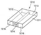
도 67은, 일본 특허 공개 평성 제 7-221537 호 공보에 제안된 안테나 장치를 도시하는 사시도이다.67 is a perspective view showing an antenna device proposed in Japanese Patent Laid-Open No. 7-221537.
안테나 장치(1210)를 구성하는 유전체 기판(1211)에는, 이 유전체 기판(1211)의 긴 변 방향으로, 방사 도체 막이 내벽에 형성된 관통 구멍(1212)이 형성되어 있다. 또한, 유전체 기판(1211)의 한쪽 단부면의 전체면에는 측면 전극(1213)이 형성되고, 다른 단부면의 중앙 부분에는 전기 공급 전극(1214)이 형성되어 있으며, 측면 전극(1213)과 전기 공급 전극(1214)은, 관통 구멍(1212)의 내벽에 형성된 방사 도체 막에 의해 전기적으로 접속되어 있다. 또한, 전기 공급 전극(1214)이 형성되어 있는 유전체 기판(1211)의 면에는 전기 공급 전극(1214)을 사이에 두도록 측면 전극(1215, 1216)이 형성되어 있다.In the
이와 같이 구성된 안테나 장치(1210)는 통신 기기 본체에 내장되는 회로 기판에 장착되고, 그 통신 기기 본체로부터 전기 공급 전극(1214)을 경유하여 안테나 장치(1210)에 고주파 전력이 공급되어, 관통 구멍(1212)의 내벽의 방사 도체 막으로부터 전자파가 방출된다.The
도 65에 도시하는 안테나 장치(990)는, 이득을 높이기 위해서는, 전자파의 주파수 대역을 좁힐 필요가 있으므로, 예컨대 휴대 전화와 같이 송수신하는 전자파의 주파수가 다른 경우는, 안테나 장치(990)를 송수신 겸용 안테나로서 이용하는 것은 곤란하다.In order to increase the gain, the antenna device 990 shown in FIG. 65 needs to narrow the frequency band of electromagnetic waves. Therefore, when the frequencies of electromagnetic waves transmitted and received, such as mobile phones, are different, for example, the antenna device 990 is used for both transmission and reception. It is difficult to use it as an antenna.
또한, 도 66 내지 도 67에 도시하는 안테나 장치(1100, 1210)는, 방사 도체 막이 형성된 관통 구멍이 연장되는 방향에 대하여 수직으로 넓어진 면내에서 무(無)지향성이다. 이러한 안테나 장치가, 예컨대 휴대 전화에 장착되는 경우, 일반적으로 휴대 전화는 수직 편파(polarized wave)의 전자파를 송수신하기 때문에, 안테나 장치는 관통 구멍이 연장되는 방향과 휴대 전화 본체의 길이 방향이 일치하도록 휴대 전화 본체에 장착된다.In addition, the
이와 같이 안테나 장치가 장착된 휴대 전화를 실제로 사람이 이용하면, 안테나 장치는 관통 구멍이 연장되는 방향에 수직인 면내에서는 무지향성이기 때문에, 안테나 장치로부터 송신되는 전자파의 일부는 인체 방향으로 조사(照射)된다. 이 인체 방향으로 조사된 전자파는 통신에는 사용되지 않는다.When a person actually uses a mobile phone equipped with an antenna device as described above, the antenna device is omnidirectional in the plane perpendicular to the direction in which the through hole extends, so that a part of the electromagnetic waves transmitted from the antenna device is irradiated toward the human body. do. Electromagnetic waves irradiated toward the human body are not used for communication.
본 발명은, 상기 사정을 감안하여 이루어진 것으로, 전자파가 효율적으로 통신에 사용되는 안테나 장치를 제공하는 것을 목적으로 한다.The present invention has been made in view of the above circumstances, and an object thereof is to provide an antenna device in which electromagnetic waves are efficiently used for communication.
상기 목적을 달성하는 본 발명의 제 1 안테나 장치는,The first antenna device of the present invention to achieve the above object,
(1) 서로 평행한 상면 및 하면을 갖는 유전체 기부 본체,(1) a dielectric base body having an upper surface and a lower surface parallel to each other,
(2) 이 유전체 기부 본체 상면에 형성되고 서로 근접한 2개의 단부를 가지며 이들 2개의 단부를 루프 형상으로 연결하는 방사 도체 막,(2) a radiating conductor film formed on an upper surface of the dielectric base body and having two ends close to each other and connecting these two ends in a loop shape,
(3) 이 유전체 기부 본체 하면에 형성되고 면형상(a planar shape)으로 넓어지는 접지 도체 막,(3) a grounding conductor film formed on the lower surface of the dielectric base body and widening in a planar shape,
(4) 이 유전체 기부 본체 측면에 형성되고 상기 방사 도체 막의 2개의 단부 각각에 접속되어 서로 평행하게 상하 방향으로 연장되며, 한쪽이 상기 접지 도체 막에 접속되어 이루어지는 전기 공급 도체 막을 구비한 것을 특징으로 한다.(4) an electric supply conductor film formed on a side surface of the dielectric base body and connected to each of the two ends of the radiation conductor film and extending in the vertical direction in parallel with each other, and one side connected to the ground conductor film; do.
본 발명의 제 1 안테나 장치에는, 유전체 기부 본체 상면에 서로 근접한 2개의 단부를 가지며, 이들 2개의 단부를 루프 형상으로 연결하는 방사 도체 막이 형성되고, 유전체 기부 본체 하면에 면형상으로 넓어지는 접지 도체 막이 형성되어 있기 때문에, 방사 도체 막의 루프면에 수직인 방향으로 최대 이득이 얻어지도록, 방사 도체 막의 길이를 공진 파장으로 하는 전자파가 방사됨과 동시에, 방사 도체 막으로부터 방사되어 접지 도체 막을 향하는 전자파는 접지 도체 막에서 반사된다. 즉, 안테나 장치로부터는 방사 도체 막을 포함하는 평면에 수직이면서, 또한 접지 도체 막으로부터 방사 도체 막을 향하는 방향으로 최대 이득의 전자파가 방사된다. 따라서, 고(高)지향성으로, 고(高)이득의 안테나 장치를 얻을 수 있으며, 이 안테나 장치를, 예컨대 휴대 전화에 부착하는 경우, 사람이 휴대 전화를 사용할 때에 접지 도체 막이 인체와 방사 도체 막 사이에 위치하도록 부착하면, 인체측에는 전자파가 방사되지 않고, 방사되는 전자파가 접지 도체 막으로부터 방사 도체 막으로 향하는 방향으로 최대 이득이면서, 효율적으로 통신에 사용된다.In the first antenna device of the present invention, a grounding conductor film having two end portions close to each other on the upper surface of the dielectric base body, and connecting the two ends in a loop shape, and a grounding conductor widening in a plane shape on the lower surface of the dielectric base body Since the film is formed, the electromagnetic wave having the length of the radiation conductor film as the resonant wavelength is radiated so that the maximum gain is obtained in the direction perpendicular to the loop surface of the radiation conductor film, while the electromagnetic wave radiated from the radiation conductor film and directed toward the ground conductor film is grounded. Reflected off the conductor film. That is, the electromagnetic wave of the maximum gain is radiated from the antenna device in a direction perpendicular to the plane including the radiation conductor film and from the ground conductor film toward the radiation conductor film. Therefore, a high gain, high gain antenna device can be obtained, and when the antenna device is attached to, for example, a mobile phone, the grounding conductor film is a human body and a radiation conductor film when a person uses the mobile phone. When attached so as to be interposed therebetween, electromagnetic waves are not radiated to the human body side, and the radiated electromagnetic waves are used for communication efficiently with maximum gain in the direction from the ground conductor film to the radiation conductor film.
또한, 본 발명의 제 1 안테나 장치는, 방사 도체 막을 형성하는 데 있어서, 유전체 기부 본체에 관통 구멍을 형성하는 것은 불필요하며, 제조 비용의 절감을 도모할 수 있다.In the first antenna device of the present invention, it is unnecessary to form through holes in the dielectric base body in forming the radiation conductor film, and the manufacturing cost can be reduced.
또한, 상기 제 1 안테나 장치의 전기 공급 도체 막이, 회로 기판의 표면에 장착할 때 전극으로도 작용하는 것이 바람직하다.Moreover, it is preferable that the electrical supply conductor film | membrane of the said 1st antenna device also acts as an electrode when it mounts on the surface of a circuit board.
전기 공급 도체 막이 회로 기판의 표면에 장착할 때 전극으로서도 작용함으로써, 이 안테나 장치가 회로 기판에 용이하게 장착된다.When the electric supply conductor film is also mounted on the surface of the circuit board, it also acts as an electrode, whereby the antenna device is easily mounted on the circuit board.
또한, 상기 목적을 달성하는 본 발명의 제 2 안테나 장치는,In addition, the second antenna device of the present invention for achieving the above object,
(1) 상면 및 하면을 가짐과 동시에 이들 상면과 하면을 연결하는 관통 구멍이 형성되어 이루어지는 유전체 기부 본체,(1) a dielectric base body having an upper surface and a lower surface and formed with a through hole connecting the upper surface and the lower surface;
(2) 상기 관통 구멍내에 충진된 단극 도체,(2) a single-pole conductor filled in said through hole,
(3) 상기 상면에 형성되고 서로 근접한 2개의 단부를 갖고, 이들 2개의 단부를 루프 형상으로 연결함과 동시에 이들 2개의 단부 중의 한쪽 단부가 상기 단극 도체에 접속되어 이루어지는 막형상(a film-like shape)의 루프 도체,(3) A film-like structure having two end portions formed on the upper surface and adjacent to each other, connecting the two end portions in a loop shape and one end of these two ends connected to the unipolar conductor. loop conductor of the shape,
(4) 상기 하면으로 넓어지는 막형상의 접지 도체를 구비한 것을 특징으로 한다.(4) A film-like grounding conductor widening to the lower surface is provided.
본 발명의 제 2 안테나 장치에는, 유전체 기부 본체의 상면에 막형상의 루프 도체가 형성되고, 유전체 기부 본체의 하면에 막형상의 접지 도체가 형성되어 있기 때문에, 막형상의 루프 도체로부터, 루프 도체의 루프면에 수직인 방향에 있어서 최대 이득의 전자파가 방사됨과 동시에, 방사된 전자파 중의, 막형상의 접지 도체로 향하는 전자파는 막형상의 접지 도체로 반사된다. 따라서, 루프 도체에 수직이면서, 또한 접지 도체로부터 루프 도체로 향하는 방향에 최대 이득의 전자파가 방사되어, 광(廣)지향성을 갖는 안테나 장치를 얻을 수 있다. 또한, 유전체 기부 본체에 형성된 관통 구멍에 단극 도체가 충진되어 있기 때문에, 단극 도체로부터, 막 형상의 루프 도체의 루프면에 평행한 방향에 있어서 최대 이득의 전자파가 방사된다. 따라서, 막형상의 접지 도체측, 즉 인체측에는 전자파가 방사되지 않고, 인체측을 제외한 다른 방향으로 전자파가 효율적으로 방사된다.In the second antenna device of the present invention, since a membrane-shaped loop conductor is formed on the upper surface of the dielectric base body and a membrane-shaped ground conductor is formed on the lower surface of the dielectric base body, the loop conductor is formed from the loop conductor of the membrane shape. While the electromagnetic wave of the maximum gain is radiated in the direction perpendicular to the loop plane of, the electromagnetic wave directed to the film-shaped ground conductor among the emitted electromagnetic waves is reflected by the film-shaped ground conductor. Therefore, the electromagnetic wave of the maximum gain is radiated | emitted perpendicularly to a loop conductor and toward the loop conductor from a ground conductor, and the antenna apparatus which has optical directivity can be obtained. In addition, since the unipolar conductor is filled in the through hole formed in the dielectric base body, the electromagnetic wave of the maximum gain is radiated from the unipolar conductor in a direction parallel to the loop surface of the loop-shaped loop conductor. Therefore, electromagnetic waves are not emitted to the film-shaped ground conductor side, that is, the human body side, and the electromagnetic waves are efficiently radiated to other directions except for the human body side.
또한, 상기 제 2 안테나 장치가 상기 하면측에서 상기 단극 도체에 접속된 중심 도체와, 상기 하면으로 넓어지는 접지 도체에 접속된 외부 도체를 갖는 동축 커넥터를 구비하여도 좋다.Moreover, the said 2nd antenna apparatus may be equipped with the coaxial connector which has the center conductor connected to the said single pole conductor at the said lower surface side, and the outer conductor connected to the ground conductor extended to the said lower surface.
동축 커넥터를 구비하면, 안테나는 동축 케이블이 접속되는 회로 기판 등에, 동축 케이블을 경유하여 접속된다.When the coaxial connector is provided, the antenna is connected to the circuit board to which the coaxial cable is connected via the coaxial cable.
또한, 상기 제 2 안테나 장치가, 상기 하면에 있어서 한쪽 단부가 상기 단극 도체에 접속된, 이 하면에 있어서 상기 접지 도체와 함께 공평면 선로(coplanar line)를 형성하는 신호선과, 상기 유전체 기부 본체의 측면에 형성되고 상기 신호선에 접속된 전기 공급 단자와, 상기 전기 공급 단자가 형성된 상기 유전체 기부 본체의 측면과 동일한 측면에 형성되고 상기 접지 도체에 접속된 접지 단자를 구비하는 것이 바람직하다.The second antenna device further includes a signal line having one end connected to the single-pole conductor on the lower surface of the second antenna device to form a coplanar line with the ground conductor on the lower surface of the lower surface of the dielectric base body. It is preferable to have an electrical supply terminal formed on a side surface and connected to the signal line, and a ground terminal formed on the same side as the side surface of the dielectric base body on which the electrical supply terminal is formed and connected to the ground conductor.
접지 도체와 함께 공평면 선로를 형성하는 신호선을 구비하면, 이 신호선의 폭이나, 신호선과 접지 도체의 갭 폭(gap widrh)이 소망하는 값으로 되도록 안테나 장치를 제조함으로써, 소망하는 선로 임피던스를 갖는 안테나 장치를 얻을 수 있다. 또한, 전기 공급 단자 및 접지 단자를 구비하면, 그 안테나 장치를 회로 기판 표면에 용이하게 장착할 수 있다.If a signal line is formed together with the ground conductor to form a coplanar line, the antenna device is manufactured such that the width of the signal line or the gap widrh of the signal line and the ground conductor is a desired value, thereby having a desired line impedance. An antenna device can be obtained. In addition, if the electrical supply terminal and the ground terminal are provided, the antenna device can be easily mounted on the circuit board surface.
또한, 상기 목적을 달성하는 본 발명의 제 3 안테나 장치는,In addition, the third antenna device of the present invention for achieving the above object,
(1) 하면 및 측면을 갖는 유전체 기부 본체,(1) a dielectric base body having a lower surface and a side surface,
(2) 상기 하면에 형성되고 면형상으로 넓어지는 접지 도체 막,(2) a grounding conductor film formed on the lower surface and widening in a plane shape,
(3) 상기 측면에 형성되고 좌우에 근접하는 2개의 단부를 갖고 이 측면을 수평으로 한번 감아서 이들 2개의 단부를 연결하는 방사 도체 막,(3) a radiating conductor film formed on the side surface and having two end portions adjacent to the left and right sides, and winding the side surface horizontally to connect these two ends,
(4) 상기 측면에 형성되고 서로 평행하게 상하 방향으로 연장되고, 1개가 상기 2개 단부 중의 한쪽에 접속되며, 다른 1개가 상기 2개의 단부 중의 다른쪽에 접속됨과 동시에 상기 접지 도체 막에 접속되어 이루어지는 2개의 전기 공급 도체 막을 구비한 것을 특징으로 한다.(4) formed on the side surface and extending in the vertical direction parallel to each other, one connected to one of the two ends, the other connected to the other of the two ends, and connected to the ground conductor film Two electrical supply conductor films are provided.
본 발명의 제 3 안테나 장치에는, 측면에, 이 측면을 수평으로 한번 감는 방사 도전체막이 형성되고, 하면에 면형상으로 넓어지는 접지 도체 막이 형성되어 있기 때문에, 방사 도체 막으로부터, 이 방사 도체 막을 포함하는 평면에 수직인 방향으로 최대 이득의 전자파가 방사됨과 동시에, 방사된 전자파 중 접지 도체 막으로 향하는 전자파는 접지 도체 막에서 반사된다. 즉, 안테나 장치로부터는, 방사 도체 막을 포함하는 평면에 수직이면서, 또한 접지 도체 막으로부터 방사 도체 막으로 향하는 방향으로 최대 이득의 전자파가 방사된다. 따라서, 이러한 안테나 장치를, 예컨대 휴대 전화에 부착하는 경우, 인간이 휴대 전화를 사용할 때에 접지 도체 막이 인간과 방사 도체 막 사이에 위치하도록 부착하면, 인체측에는 전자파가 방사되지 않고, 전자파가 접지 도체 막으로부터 방사 도체 막으로 향하는 방향에 최대 이득으로, 효율적으로 통신에 사용된다.In the third antenna device of the present invention, since the radiation conductor film is formed on the side surface and is wound horizontally once, and the ground conductor film is formed on the lower surface in a planar shape, the radiation conductor film is removed from the radiation conductor film. At the same time as the electromagnetic wave of the maximum gain is radiated in the direction perpendicular to the containing plane, the electromagnetic wave directed toward the ground conductor film among the emitted electromagnetic waves is reflected by the ground conductor film. That is, from the antenna device, the electromagnetic wave of maximum gain is radiated in the direction perpendicular to the plane including the radiation conductor film and from the ground conductor film to the radiation conductor film. Therefore, when attaching such an antenna device to, for example, a mobile phone, if a ground conductor film is attached between the human and the radiation conductor film when a human uses the mobile phone, electromagnetic waves are not radiated to the human body side, and the electromagnetic wave is the ground conductor film. It is used for communication efficiently with the maximum gain in the direction from the to the radiating conductor film.
또한, 본 발명의 제 3 안테나 장치는, 방사 도체 막을 형성하는 데 있어서, 유전체 기부 본체에 관통 구멍을 형성하는 것이 불필요하여, 제조 비용의 절감을 도모할 수 있다.Further, in the third antenna device of the present invention, it is unnecessary to form through holes in the dielectric base body in forming the radiation conductor film, so that the manufacturing cost can be reduced.
여기서, 본 발명의 제 3 안테나 장치는, 2개의 전기 공급 도체 막이 회로 기판의 표면에 장착할 때 전극으로서도 작용하는 것이 바람직하다.Here, it is preferable that the 3rd antenna device of this invention also acts as an electrode when two electrical supply conductor films are mounted on the surface of a circuit board.
전기 공급 도체 막이 회로 기판의 표면에 장착할 때 전극으로서도 작용함으로써, 이 안테나 장치를 회로 기판에 용이하게 장착하는 것이 가능하다.By acting also as an electrode when the electric supply conductor film is mounted on the surface of the circuit board, it is possible to easily mount this antenna device on the circuit board.
또한, 상기 목적을 달성하는 본 발명의 제 4 안테나 장치는,In addition, the fourth antenna device of the present invention for achieving the above object,
(1) 하면을 갖는 유전체 기부 본체,(1) a dielectric base body having a lower surface,
(2) 이 유전체 기부 본체의 하면에 형성되고 면형상으로 넓어지는 접지 도체 막,(2) a grounding conductor film formed on the lower surface of the dielectric base body and widening in planar shape,
(3) 상기 유전체 기부 본체의 내부에 형성되고 좌우에 근접하는 2개의 단부를 갖고, 수평면내를 루프 형상으로 한번 감아서 이들 2개의 단부를 연결하는 방사 도체 막,(3) a radiating conductor film having two ends formed inside the dielectric base body and proximate to the left and right, and winding the inside of the horizontal plane in a loop shape once to connect these two ends,
(4) 상기 유전체 기부 본체의 내부에 형성되고 상기 방사 도체 막의 2개의 각각의 단부와 상기 유전체 기부 본체의 측면을 연결하는 내부 전기 공급 도체 막,(4) an internal electrical supply conductor film formed inside said dielectric base body and connecting two respective ends of said radiating conductor film with the side of said dielectric base body,
(5) 상기 유전체 기부 본체의 측면에 형성되고 서로 평행하게 상하 방향으로 연장되어 내부 전기 공급 도체 막 각각에 접속됨과 동시에, 한쪽이 상기 접지 도체 막에 접속되어 이루어지는 측면 전기 공급 도체 막을 구비한 것을 특징으로 한다.(5) A side electric supply conductor film is formed on the side surface of said dielectric base body and extends in the vertical direction in parallel to each other and is connected to each of the internal electric supply conductor films, and one side is connected to said ground conductor film. It is done.
본 발명의 제 4 안테나 장치에는, 내부에, 수평면내를 루프 형상으로 한번 감는 방사 도체 막이 형성되고, 하면에, 면형상으로 넓어지는 접지 도체 막이 형성되어 있기 때문에, 방사 도체 막으로부터 이 방사 도체 막을 포함하는 평면에 수직인 방향으로 최대 이득의 전자파가 방사됨과 동시에, 방사된 전자파 중 접지 도체 막으로 향하는 전자파는 접지 도체 막에서 반사된다. 즉, 안테나 장치로부터는 방사 도체 막을 포함하는 평면에 수직이면서, 또한 접지 도체 막으로부터 방사 도체 막으로 향하는 방향으로 최대 이득의 전자파가 방사된다. 따라서, 이러한 안테나 장치를, 예컨대 휴대 전화에 부착하는 경우, 사람이 휴대 전화를 사용할 때 접지 도체 막이 인체와 방사 도체 막 사이에 위치하도록 부착하면, 인체측에는 전자파가 방사되지 않고, 방사되는 전자파는, 접지 도체 막으로부터 방사 도체 막으로 향하는 방향으로 최대 이득으로, 효율적으로 통신에 사용된다.In the fourth antenna device of the present invention, since the radiation conductor film is formed inside the horizontal plane once in a loop shape, and the ground conductor film widening in the plane shape is formed on the lower surface, the radiation conductor film is removed from the radiation conductor film. At the same time as the electromagnetic wave of the maximum gain is radiated in the direction perpendicular to the containing plane, the electromagnetic wave directed toward the ground conductor film among the emitted electromagnetic waves is reflected by the ground conductor film. That is, the electromagnetic wave of the maximum gain is radiated from the antenna device in the direction perpendicular to the plane including the radiation conductor film and from the ground conductor film to the radiation conductor film. Therefore, when attaching such an antenna device to, for example, a mobile phone, if a ground conductor film is attached between the human body and the radiation conductor film when a person uses the mobile phone, electromagnetic waves are not radiated to the human body side, and the radiated electromagnetic waves are It is used for communication efficiently with maximum gain in the direction from the ground conductor film to the radiation conductor film.
그런데, 동일 주파수의 전자파에 있어서, 공기중에 있어서의 전자파의 파장과 유전체 중에 있어서의 전자파의 파장을 비교하면, 유전체 중의 것이 전자파 파장이 짧다. 따라서, 방사 도체 막을 유전체 기부 본체의 내부에 형성한 경우와 방사 도체 막을 유전체 기부 본체의 표면에 형성한 경우를 비교하면, 같은 주파수의 전자파를 방사하는 경우, 내부에 방사 도체 막을 형성한 쪽이 방사 도체 막의 루프의 길이를 짧게 할 수 있다. 이와 같이 방사 도체 막의 루프의 길이를 짧게 하는 것이 가능하면, 유전체 기부 본체의 치수를 작게 하는 것이 가능하다.By the way, when the electromagnetic wave of the same frequency is compared with the wavelength of the electromagnetic wave in air, and the wavelength of the electromagnetic wave in a dielectric material, the electromagnetic wave wavelength is short. Therefore, when the radiation conductor film is formed inside the dielectric base body and the radiation conductor film is formed on the surface of the dielectric base body, when the electromagnetic wave of the same frequency is radiated, the radiation conductor film is formed inside. The length of the loop of the conductor membrane can be shortened. In this way, if the length of the loop of the radiating conductor film can be shortened, it is possible to reduce the dimensions of the dielectric base body.
따라서, 방사 도체 막이 유전체 기부 본체의 내부에 형성된 본 발명의 제 4 안테나 장치로는 소형화를 실현할 수 있다.Accordingly, the fourth antenna device of the present invention in which the radiating conductor film is formed inside the dielectric base body can be miniaturized.
또한, 본 발명의 제 4 안테나 장치는, 방사 도체 막을 형성하는 데 있어서, 유전체 기부 본체에 관통 구멍을 형성하는 것은 불필요하므로, 제조 비용의 절감을 도모할 수 있다.Further, in the fourth antenna device of the present invention, it is unnecessary to form through holes in the dielectric base body when forming the radiation conductor film, so that the manufacturing cost can be reduced.
여기서, 본 발명의 제 4 안테나 장치에 있어서, 상기 전기 공급 도체 막이 회로 기판의 표면에 장착할 때 전극으로서도 작용하는 것이 바람직하다.Here, in the fourth antenna device of the present invention, it is preferable that the electric supply conductor film also acts as an electrode when mounted on the surface of the circuit board.
전기 공급 도체 막이 회로 기판의 표면에 장착할 때 전극으로서도 작용함으로써, 이 안테나 장치를 회로 기판에 용이하게 장착할 수 있다.When the electric supply conductor film is also mounted on the surface of the circuit board, it also acts as an electrode, whereby the antenna device can be easily mounted on the circuit board.
또한, 상기 목적을 달성하는 본 발명의 제 5 안테나 장치는,In addition, the fifth antenna device of the present invention for achieving the above object,
(1) 수평으로 넓어지는 상면 및 하면을 갖는 유전체 기부 본체,(1) a dielectric base body having an upper surface and a lower surface widening horizontally,
(2) 상기 유전체 기부 본체의 하면에 형성되고 면형상으로 넓어지는 접지 도체 막,(2) a grounding conductor film formed on the lower surface of the dielectric base body and widening in a plane shape,
(3) 상기 유전체 기부 본체의 상면에 형성되고 소정의 제 1 갭을 사이에 두고 서로 마주 보는 2개의 단부가 형성되도록 이 상면내를 한번 감는 제 1 루프 방사 도체 막,(3) a first loop radiating conductor film formed on the upper surface of the dielectric base body and wound around the upper surface once so that two ends facing each other with a predetermined first gap therebetween are formed;
(4) 상기 유전체 기부 본체의 내부에 형성되고 상기 제 1 루프 방사 도체 막의 루프에 대한 상기 제 1 갭의 방향과는 방향이 다른 제 2 갭을 사이에 두고 서로 마주 보는 2개의 단부가 형성되도록 수평면내를 한번 감는 제 2 루프 방사 도체 막,(4) a horizontal plane formed inside the dielectric base body and having two end portions facing each other with a second gap interposed between the first gap and the direction of the first gap with respect to the loop of the first loop radiating conductor film; Second loop radiating conductor membrane, winding once inside
(5) 각각이 상기 제 1 루프 방사 도체 막의 2개의 단부 각각에 접속되고, 서로 평행하게 연장되어 있으며, 한쪽이 상기 접지 도체 막에 접속되어 이루어지는 2개의 제 1 전기 공급 도체 막,(5) two first electric supply conductor films, each connected to each of two ends of the first loop radiating conductor film, extending in parallel to each other, and one connected to the ground conductor film;
(6) 각각이 상기 제 2 루프 방사 도체 막의 2개의 단부 각각에 접속되고, 서로 평행하게, 상기 유전체 기부 본체의 측면을 경유하여 연장되어 있으며 한쪽이 상기 접지 도체 막에 접속되어 이루어지는 2개의 제 2 전기 공급 도체 막을 구비한 것을 특징으로 한다.(6) two second, each of which is connected to each of two ends of the second loop radiating conductor film, extends in parallel to each other via a side surface of the dielectric base body, and one of which is connected to the ground conductor film; An electric supply conductor film is provided.
본 발명의 제 5 안테나 장치에서는, 루프에 대한 갭의 방향이 서로 다른 제 1 루프 방사 도체 막 및 제 2 루프 방사 도체 막이 구비되어 있기 때문에, 제 1 루프 방사 도체 막에 의해 송수신되는 전자파의 편파 방향과, 제 2 루프 방사 도체 막에 의해 송수신되는 전자파의 편파 방향이 서로 다르다. 따라서, 1개의 안테나 장치로 서로 다른 편파 방향의 전자파를 송수신하는 것이 가능하다.In the fifth antenna device of the present invention, since the first loop radiation conductor film and the second loop radiation conductor film having different directions of the gap with respect to the loop are provided, the polarization direction of the electromagnetic wave transmitted and received by the first loop radiation conductor film is provided. And the polarization directions of the electromagnetic waves transmitted and received by the second loop radiation conductor film are different from each other. Therefore, it is possible to transmit and receive electromagnetic waves in different polarization directions with one antenna device.
또한, 본 발명의 제 5 안테나 장치는, 유전체 기부 본체의 상면내를 한번 감는 제 1 루프 방사 도체 막과, 유전체 기부 본체의 내부에, 수평면내를 한번 감는 제 2 루프 방사 도체 막을 구비하고 있기 때문에, 루프 안테나 구조를 가지며, 제 1, 제 2 루프 방사 도체 막으로부터 방출되는 전자파는, 이 방사 도체 막을 포함하는 평면에 수직인 방향으로 최대 이득의 전자파이다. 또한, 유전체 기부 본체의 하면에는 접지 도체 막이 형성되어 있기 때문에, 제 1, 제 2 루프 방사 도체 막으로부터 방출된 전자파 중 접지 도체 막으로 향하는 전자파는 이 접지 도체 막에서 반사된다. 즉, 안테나 장치로부터는, 접지 도체 막으로부터 제 1, 제 2 루프 방사 도체 막으로 향하는 방향으로 최대 이득의 전자파가 방사된다. 따라서, 본 발명의 제 5 안테나 장치를, 예컨대 휴대 전화에 부착하는 경우에, 사람이 휴대 전화를 사용할 때 접지 도체 막이 인체와 루프 방사 도체 막 사이에 위치하도록 부착하면, 인체측에는 전자파가 방사되지 않고, 방사되는 전자파는 접지 도체 막으로부터 방사 도체 막으로 향하는 방향으로 최대 이득이며, 효율적으로 통신에 사용된다.In addition, the fifth antenna device of the present invention includes a first loop radiating conductor film wound once in the upper surface of the dielectric base body, and a second loop radiating conductor film wound once in the horizontal plane inside the dielectric base body. Has a loop antenna structure, and the electromagnetic waves emitted from the first and second loop radiating conductor films are electromagnetic waves of maximum gain in a direction perpendicular to the plane containing the radiating conductor film. In addition, since a ground conductor film is formed on the lower surface of the dielectric base body, electromagnetic waves directed to the ground conductor film among the electromagnetic waves emitted from the first and second loop radiating conductor films are reflected by the ground conductor film. That is, the electromagnetic wave of a maximum gain is radiated | emitted from an antenna device in the direction from a ground conductor film to a 1st, 2nd loop radiation conductor film. Therefore, when attaching the fifth antenna device of the present invention to, for example, a mobile phone, if a ground conductor film is attached so that a person is located between the human body and the loop radiation conductor film when using the mobile phone, electromagnetic waves are not radiated to the human body side. The radiated electromagnetic wave is the maximum gain in the direction from the ground conductor film to the radiation conductor film, and is effectively used for communication.
여기서, 본 발명의 제 5 안테나 장치는, 제 1 루프 방사 도체 막 및 제 2 루프 방사 도체 막이, 제 1 루프 방사 도체 막의 루프에 대한 제 1 갭의 방향과, 제 2 방사 도체 막의 루프에 대한 제 2 갭의 방향이 수평면내에서 서로 90°다른 방향이 되도록 형성되는 것이 바람직하다.In the fifth antenna device of the present invention, the first loop radiating conductor film and the second loop radiating conductor film are formed in the direction of the first gap with respect to the loop of the first loop radiating conductor film, and with respect to the loop of the second radiating conductor film. It is preferable that the directions of the two gaps are formed to be in directions different from each other by 90 ° in the horizontal plane.
이와 같이, 제 1 루프 방사 도체 막 및 제 2 루프 방사 도체 막을 형성하면, 전자파가 수직 편파 또는 수평 편파라도 전자파를 효율적으로 수신할 수 있다.In this manner, when the first loop radiation conductor film and the second loop radiation conductor film are formed, the electromagnetic waves can be efficiently received even if the electromagnetic waves are vertically or horizontally polarized.
또한, 본 발명의 제 5 안테나 장치는, 방사 도체 막을 형성하는 데 있어서, 유전체 기부 본체에 관통 구멍을 형성하는 것은 불필요하여, 제조 비용의 절감을 도모할 수 있다.Further, in the fifth antenna device of the present invention, it is unnecessary to form through holes in the dielectric base body in forming the radiation conductor film, and the manufacturing cost can be reduced.
여기서, 본 발명의 제 5 안테나 장치는, 제 1, 제 2 전기 공급 도체 막이 회로 기판의 표면에 장착할 때 전극으로서도 작용하는 것이 바람직하다.Here, it is preferable that the fifth antenna device of the present invention also acts as an electrode when the first and second electric supply conductor films are mounted on the surface of the circuit board.
전기 공급 도체 막이 회로 기판의 표면에 장착할 때 전극으로서도 작용으로써, 이 안테나 장치를 회로 기판에 용이하게 장착할 수 있다.When the electric supply conductor film is mounted on the surface of the circuit board, it also acts as an electrode, whereby the antenna device can be easily mounted on the circuit board.
또한, 상기 목적을 달성하는 본 발명의 제 6 안테나 장치는,In addition, the sixth antenna device of the present invention for achieving the above object,
(1) 상면, 하면 및 측면을 갖는 유전체 기부 본체,(1) a dielectric base body having an upper surface, a lower surface and a side surface,
(2) 상기 유전체 기부 본체의 하면에 형성된 접지 도체 막,(2) a ground conductor film formed on the lower surface of the dielectric base body,
(3) 상기 유전체 기부 본체의 상면 또는 측면에 형성되고 수평 방향으로 연장되어 인접하는 단부끼리가 갭을 사이에 두고 서로 마주 봄과 동시에, 전체로서 등간격으로 4개의 갭을 형성하여 한번 감는 4개의 방사 도체 막,(3) Four windings formed on the upper surface or the side surface of the dielectric base body and extending in the horizontal direction so that adjacent ends face each other with a gap therebetween, and form four gaps at equal intervals as a whole. Radiation conductor membrane,
(4) 각각이 상기 4개의 방사 도체 막의 각 단부 각각에 접속되어 상하 방향으로 연장되어 있는 8개의 전기 공급 도체 막을 구비한 것을 특징으로 한다.(4) Each of the four radiating conductor films is characterized by comprising eight electric supply conductor films connected to each end of each of the four radiating conductor films and extending in the vertical direction.
본 발명의 제 6 안테나 장치는, 전체로서 한번 감는 방사 도체 막을 구비하고 있기 때문에, 루프 안테나 구조를 갖는다.Since the sixth antenna device of the present invention includes a radiation conductor film wound once as a whole, it has a loop antenna structure.
도 1은 루프 안테나 구조를 갖는 안테나 장치의 작용 설명도이다.1 is an explanatory view of the operation of an antenna device having a loop antenna structure.
도 1은 안테나 장치(10)의 평면도이고, 안테나 장치(10)를 구성하는 유전체 기부 본체(11)의 표면에, 서로 근접한 2개의 단부(12a, 12b)끼리가 갭을 사이에 두고 서로 마주 봄과 동시에, 점 0를 중심으로 하여 원형 루프 형상으로 일주하여 이들 2개의 단부(12a, 12b)를 연결하는 방사 도체 막(12)이 형성되어 있으며, 이 방사 도체 막(12)의 길이는 송수신 대상인 전자파의 공진 파장과 동일한 길이로 조정되어 있다. 또한, 점 A는 2개의 단부(12a, 12b)의 위치를 도시하는 점이며, 점 B, C, D는, 각각 점 A에서 시계 방향으로 점 0를 중심으로 하여 90°, 180°, 270° 회전한 위치에 있는 점이다.FIG. 1 is a plan view of the
이와 같이 구성된 안테나 장치(10)에서는, 2개의 단부(12a, 12b) 사이에 전압이 인가되면, 2개의 단부(12a, 12b)로부터 방사 도체 막(12)에 전류가 공급되어, 방사 도체 막(12)상에 정재파(a standing wave)가 발생하며, 방사 도체 막(12)에 흐르는 전류는, 점 A와 점 C에서 최대이며, 점 B와 점 D에서 거의 0으로 된다. 이 최대 전류가 흐르는 점 A 및 점 C에서는, 전류의 방향은 점 B와 점 D를 연결하는 선에 따른 방향으로 된다. 따라서, 편파 방향은 점 B와 점 D를 연결하는 선에 따른 방향으로 된다.In the
도 2는, 도 1에 도시한 방사 도체 막 대신에, 도 1에 도시한 점 C의 위치에도 전기 공급점을 마련한, 전체적으로 루프 형상을 하는 방사 도체 막을 채용하여 구성된 안테나 장치의 작용 설명도이다.FIG. 2 is an explanatory view of the operation of the antenna device employing the loop-shaped radiation conductor film as a whole, in which an electric supply point is also provided at the point C shown in FIG. 1 instead of the radiation conductor film shown in FIG. 1.
이와 같이 구성된 안테나 장치(20)에서는, 점 A 및 점 C에서 동일 진폭 동일 위상의 전류가 공급되면, 방사 도체 막(22)상에 정재파가 발생하고, 방사 도체 막(22)에 흐르는 전류는 도 1에 도시하는 안테나 장치(10)와 같이 점 A 및 점 C에 있어서 최대이며, 점 B 및 점 D에 있어서 거의 0으로 된다. 이 최대 전류가 흐르는 점 A 및 점 C에 있어서는, 전류의 방향은 점 B와 점 D를 연결하는 선에 따른 방향이 된다. 따라서, 편파 방향은 도 1에 도시하는 안테나 장치(10)와 마찬가지로 점 B와 점 D를 연결하는 면에 따른 방향으로 된다.In the
도 3은, 도 2에 도시한 방사 도체 막 대신에, 도 2에 도시한 점 B 및 점 D의 위치에도 전기 공급점을 설치한, 전체적으로 루프 형상을 하는 방사 도체 막을 채용하여 구성된 안테나 장치의 작용 설명도이다.FIG. 3 is an operation of an antenna device configured by employing an overall loop-shaped radiation conductor film in which electric supply points are also provided at positions B and D shown in FIG. 2 instead of the radiation conductor film shown in FIG. It is explanatory drawing.
이와 같이 구성된 안테나 장치(30)에서는, 이 안테나 장치를 구성하는 방사 도체 막(32)은, 전류가 거의 0으로 되는 점 B 및 점 D의 위치에서 루프가 절단되어 있기 때문에, 도 2에 도시하는 안테나 장치(20)와 같이, 점 A 및 점 C에서 동일 진폭 동일 위상의 전류가 공급되면, 방사 도체 막(32)상에 정재파가 발생하고, 방사 도체 막(32)에 흐르는 전류는 점 A와 점 C에 있어서 최대이며, 점 B 및 점 D에서 0으로 된다. 이 최대 전류가 흐르는 점 A 및 점 C에서는, 전류의 방향은 점 B와 점 D를 연결하는 선에 따른 방향으로 된다. 따라서, 편파 방향은 도 2에 도시한 안테나 장치(20)와 같이 점 B와 점 D를 연결하는 선을 따른 방향으로 된다. 한편, 점 A 및 점 C 대신에 점 B 및 점 D에서, 동일 진폭 동일 위상의 전류가 공급되면, 방사 도체 막(32)상에 정재파가 발생하여, 방사 도체 막(32)에 흐르는 전류는 점 B 및 점 D에서 최대이며, 점 A 및 점 C에서 0으로 된다. 이 최대 전류가 흐르는 점 B 및 점 D에서는, 전류의 방향은 점 A와 점 C를 연결하는 선을 따른 방향으로 되고, 편파 방향은 점 A와 점 C를 연결하는 선을 따른 방향으로 된다.In the
따라서, 점 A 및 점 C에 동일 진폭 동일 위상의 전류를 공급하는 상태와, 점 B 및 점 D에 동일 진폭 동일 위상의 전류를 공급하는 상태를 전환이 자유롭도록 구성하면, 서로 수직으로 교차하는 편파 방향으로 전환이 자유롭도록 이득을 갖는 안테나 장치를 얻을 수 있다.Therefore, when the state which supplies the current of the same amplitude and same phase to the point A and the point C, and the state which supplies the current of the same amplitude and the same phase to the point B and the point D is comprised so that switching is free, a polarization which mutually perpendicularly crosses each other An antenna device having a gain can be obtained so that switching in the direction is free.
또한, 본 발명의 제 6 안테나 장치는, 도 3에 도시하는 바와 같이 수평 방향으로 연장되어 인접하는 단부끼리가 갭을 사이에 두고 서로 마주 봄과 동시에, 전체적으로 등간격으로 4개의 갭을 형성하여 한번 감는 4개의 방사 도체 막이 형성되어 있기 때문에, 서로 수직으로 교차하는 편파 방향의 전자파를 송수신할 수 있다.In addition, as shown in FIG. 3, the sixth antenna device of the present invention extends in the horizontal direction and adjacent edges face each other with a gap therebetween, and form four gaps at equal intervals as a whole. Since four winding conductor films are formed, it is possible to transmit and receive electromagnetic waves in a polarization direction perpendicular to each other.
또한, 본 발명의 제 6 안테나 장치는, 방사 도체 막을 형성하는 데 있어서, 유전체 기부 본체에 관통 구멍을 형성하는 것은 불필요하므로, 제조 비용의 절감을 도모할 수 있다.Further, in the sixth antenna device of the present invention, it is unnecessary to form through holes in the dielectric base body when forming the radiation conductor film, so that the manufacturing cost can be reduced.
또한, 상기 제 6 안테나 장치의 전기 공급 도체 막이 회로 기판의 표면에 장착할 때 전극으로서도 작용하는 것이 바람직하다.In addition, it is preferable that the electric supply conductor film of the sixth antenna device also serves as an electrode when mounted on the surface of the circuit board.
전기 공급 도체 막이 회로 기판의 표면에 장착할 때 전극으로서도 작용함으로써, 이 안테나 장치를 회로 기판에 용이하게 장착할 수 있다.When the electric supply conductor film is also mounted on the surface of the circuit board, it also acts as an electrode, whereby the antenna device can be easily mounted on the circuit board.
또한, 상기 목적을 달성하는 본 발명의 제 7 안테나 장치는,In addition, the seventh antenna device of the present invention for achieving the above object,
(1) 유전체 기부 본체,(1) the dielectric base body,
(2) 이 유전체 기부 본체에 형성되고 수평으로 한번 감는 폐루프 형상의 방사 도체 막,(2) a closed-loop radiated conductor film formed on the dielectric base body and wound once horizontally,
(3) 이 유전체 기부 본체에 형성되고 수평으로 넓어지는 접지 도체 막,(3) a grounding conductor film formed on the dielectric base body and widening horizontally,
(4) 이 유전체 기부 본체 측면을 경유하여 서로 평행하게 상하 방향으로 연장되며 양쪽이 상기 방사 도체 막에 접속되어 이루어지는 한 쌍의 전기 공급 도체 막을 구비한 것을 특징으로 한다.(4) A pair of electric supply conductor films is provided, which extend in the vertical direction in parallel with each other via the dielectric base body side surface, and both are connected to the radiation conductor film.
본 발명의 제 7 안테나 장치는, 유전체 기부 본체에 수평으로 한번 감는 폐루프 형상의 방사 도체 막이 형성되어 있기 때문에, 1파장 루프 안테나 구조를 가지며, 방사 도체 막으로부터 방출되는 전자파는 이 방사 도체 막을 포함하는 평면에 수직인 방향으로 최대 이득의 전자파이다. 또한, 유전체 기부 본체에는 수평으로 넓어지는 접지 도체 막이 형성되어 있기 때문에, 방사 도체 막으로부터 방출된 전자파 중 접지 도체 막으로 향하는 전자파는 접지 도체 막에서 반사된다. 즉, 안테나 장치로부터는 방사 도체 막을 포함하는 평면에 수직이면서, 또한 접지 도체 막으로부터 방사 도체 막으로 향하는 방향으로 최대 이득의 전자파가 방사된다. 따라서, 본 발명의 제 7 안테나 장치를, 예컨대 휴대 전화에 부착하는 경우, 사람이 휴대 전화를 사용할 때 접지 도체 막이 인체와 방사 도체 막 사이에 위치하도록 부착하면, 인체측에는 전자파가 방사되지 않고, 방사되는 전자파는 접지 도체 막으로부터 방사 도체 막으로 향하는 방향으로 최대 이득이면서, 효율적으로 통신에 사용된다.The seventh antenna device of the present invention has a one-wavelength loop antenna structure because a closed loop radiation conductor film wound around the dielectric base body is formed once, and the electromagnetic wave emitted from the radiation conductor film includes the radiation conductor film. It is the electromagnetic wave of maximum gain in the direction perpendicular to the plane. In addition, since a ground conductor film that is horizontally widened is formed in the dielectric base body, electromagnetic waves directed to the ground conductor film among the electromagnetic waves emitted from the radiation conductor film are reflected by the ground conductor film. That is, the electromagnetic wave of the maximum gain is radiated from the antenna device in the direction perpendicular to the plane including the radiation conductor film and from the ground conductor film to the radiation conductor film. Therefore, when the seventh antenna device of the present invention is attached to, for example, a mobile phone, if a person attaches the ground conductor film to be located between the human body and the radiation conductor film when using the mobile phone, electromagnetic waves are not radiated to the human body side, The electromagnetic waves to be used are efficiently used for communication with maximum gain in the direction from the ground conductor film to the radiation conductor film.
또한, 본 발명의 제 7 안테나 장치는, 방사 도체 막을 형성하는 데 있어서, 유전체 기부 본체에 관통 구멍을 형성하는 것이 불필요하여, 제조 비용의 절감을 도모할 수 있다.Further, in the seventh antenna device of the present invention, it is unnecessary to form the through hole in the dielectric base body in forming the radiation conductor film, so that the manufacturing cost can be reduced.
여기서 본 발명의 제 7 안테나 장치의 방사 도체 막이, 상기 유전체 기부 본체 상면내로 한번 감는 폐루프 형상의 방사 도체 막, 또는 상기 유전체 기부 본체 측면을 수평으로 주회(周回)하는 폐루프 형상의 방사 도체 막이어도 좋다.Here, a closed-loop radiated conductor film in which the radiating conductor film of the seventh antenna device of the present invention is once wound into the upper surface of the dielectric base body, or a closed-loop radiating conductor film wound around the dielectric base body side horizontally. It may be.
또한, 본 발명의 제 7 안테나 장치의 방사 도체 막이, 상기 유전체 기부 본체 내부의 수평면내에서 한번 감는 폐루프 형상의 방사 도체 막이어도 좋다.The radiation conductor film of the seventh antenna device of the present invention may be a closed loop radiation conductor film that is wound once in a horizontal plane inside the dielectric base body.
동일 주파수의 전자파에 있어서, 공기중에 있어서의 전자파의 파장과 유전체 중에 있어서의 전자파의 파장을 비교하면, 유전체중의 것이 전자파의 파장이 짧기 때문에, 방사 도체 막을 유전체 기부 본체의 내부에 형성하면 방사 도체 막의 루프의 길이를 짧게 하는 것이 가능하다. 따라서, 유전체 기부 본체의 치수를 작게 할 수 있어 안테나 장치의 소형화를 도모할 수 있다.For electromagnetic waves of the same frequency, when the wavelength of the electromagnetic wave in the air and the wavelength of the electromagnetic wave in the dielectric are compared, since the wavelength of the electromagnetic wave is short, the radiation conductor film is formed inside the main body of the dielectric base. It is possible to shorten the length of the loop of the membrane. Therefore, the dimension of the dielectric base body can be made small and the antenna device can be miniaturized.
여기서, 본 발명의 제 7 안테나 장치가, 상기 방사 도체 막외에, 상기 유전체 기부 본체의, 이 방사 도체 막이 형성된 위치와는 다른 위치에, 수평으로 한번 감는 폐루프 형상의 제 2 방사 도체 막을 구비함과 동시에,Here, the seventh antenna device of the present invention includes, in addition to the radiation conductor film, a closed-loop second radiation conductor film wound horizontally at a position different from the position where the radiation conductor film is formed on the dielectric base body. At the same time,
상기 유전체 기부 본체 측면의, 상기 한 쌍의 전기 공급 도체 막이 형성된 위치와는 다른 위치를 경유하여 서로 평행하게 상하 방향으로 연장되어 양쪽이 상기 제 2 방사 도체 막에 접속되어 이루어지는 한 쌍의 제 2 전기 공급 도체 막을 구비하는 것이 바람직하다.A pair of second electrics on the side of the dielectric base body extending in the vertical direction parallel to each other via a position different from the position where the pair of electric supply conductor films are formed, and both are connected to the second radiating conductor film. It is preferred to have a feed conductor membrane.
상기 한 쌍의 전기 공급 도체 막 및 상기 제 2 한 쌍의 전기 공급 도체 막이, 유전체 기부 본체 측면의 서로 다른 위치를 경유하도록 형성되면, 한 쌍의 전기 공급 도체 막에 접속되는 방사 도체 막 및 상기 제 2 한 쌍의 전기 공급 도체 막에 접속되는 제 2 방사 도체 막은 송수신하는 전자파의 편파 방향이 서로 다르다. 이하에, 각각의 방사 도체 막에 대하여 송수신하는 전자파의 편파 방향이 다른 이유를 설명한다.A radiating conductor film and the first conductive film connected to the pair of electric supply conductor films when the pair of electric supply conductor films and the second pair of electric supply conductor films are formed to pass through different positions on the side of the dielectric base body. 2 The 2nd radiation conductor film connected to a pair of electrical supply conductor film | membrane differs from the polarization direction of the electromagnetic wave which transmits and receives. The reason why the polarization directions of the electromagnetic waves transmitted and received for each of the radiation conductor films are different will be described below.
도 4는 그 설명도이다.4 is an explanatory diagram thereof.
도 4는 안테나 장치(40)의 평면도이고, 안테나 장치(40)를 구성하는 원주 형상의 유전체 기부 본체(41)의 표면에, 점 0를 중심으로 하여 상면의 원주를 따라 수평으로 한번 감는 원형의 폐루프 형상의 방사 도체 막(42)이 형성되어 있다. 또한, 점 A는 이 방사 도체 막(42)과 한 쌍의 전기 공급 도체 막(도시하지 않음)과의 접속점이고, 점 B, C, D는 각각 점 A로부터 시계 방향으로 점 0를 중심으로 90°, 180°, 270°회전한 위치에 있는 점이다.4 is a plan view of the antenna device 40, and is circularly wound once horizontally along the circumference of the upper surface around the point 0 on the surface of the cylindrical dielectric base body 41 constituting the antenna device 40. A closed loop radiation conductor film 42 is formed. In addition, point A is a connection point of this radiating conductor film 42 and a pair of electric supply conductor film (not shown), and points B, C, and D are respectively 90 centered on point 0 clockwise from point A. It is a point that is rotated °, 180 °, 270 °.
이와 같이 구성된 안테나 장치(40)는, 폐루프 형상의 방사 도체 막(42)이 형성되어 있기 때문에, 1파장 루프 안테나 구조를 가지며, 점 A에서 방사 도체 막(42)에 전류가 공급되면 방사 도체 막(42)상에 정재파가 발생하여, 방사 도체 막(42)에 흐르는 전류는, 점 A와 점 C에서 최대이고, 점 B와 점 D에 있어서는 거의 0으로 된다. 이 최대 전류가 흐르는 점 A 및 점 C에 있어서는, 전류의 방향은 점 B와 점 D를 연결하는 선을 따른 방향으로 되고, 편파 방향은 점 B와 점 D를 연결한 선을 따른 방향으로 된다. 따라서, 점 A에서 방사 도체 막(42)에 전류를 공급하는 대신에, 예컨대, 점 B에서 방사 도체 막(42)에 전류를 공급하면, 편파 방향은 점 A 와 점 C를 연결하는 선을 따른 방향으로 되어, 점 A에서 방사 도체 막(42)에 전류를 공급하는 경우와, 점 B에서 방사 도체 막(42)에 전류를 공급하는 경우를 비교하면, 편파 방향은 서로 수직으로 된다.The antenna device 40 configured as described above has a one-wavelength loop antenna structure because the closed loop radiation conductor film 42 is formed, and when the current is supplied to the radiation conductor film 42 at the point A, the radiation conductor A standing wave is generated on the film 42, and the current flowing through the radiation conductor film 42 is maximum at points A and C, and becomes almost zero at points B and D. FIG. In the points A and C through which the maximum current flows, the direction of the current is in the direction along the line connecting the points B and D, and the polarization direction is in the direction along the line connecting the points B and D. Thus, instead of supplying current to the radiation conductor film 42 at point A, for example, at a point B to supply current to the radiation conductor film 42, the polarization direction is along the line connecting point A and point C. Direction, the polarization direction becomes perpendicular to each other when the current is supplied to the radiation conductor film 42 at the point A and the current is supplied to the radiation conductor film 42 at the point B.
상술한 바와 같이, 제 2 방사 도체 막에 접속되는 한 쌍의 제 2 전기 공급도체 막은, 상기 방사 도체 막에 접속된 상기 한 쌍의 전기 공급 도체 막이 경유하는 위치와는 다른 위치를 경유하기 때문에, 상기 방사 도체 막과 제 2 방사 도체 막을 비교하면, 전류가 공급되는 점은 수평면내에서 서로 다르다. 따라서, 도 4를 참조하여 설명한 바와 같이, 상기 방사 도체 막에 의해 송수신되는 전자파의 편파 방향과, 제 2 방사 도체 막에 의해 송수신되는 전자파의 편파 방향은 서로 다르다는 것을 알 수 있다. 따라서, 상기 한 쌍의 전기 공급 도체 막 및 상기 제 2 한쌍의 전기 공급 도체 막이 유전체 기부 본체 측면의 서로 다른 위치를 경유하도록 형성되면, 1개의 안테나 장치로 서로 다른 편파 방향의 전자파를 송수신하는 것이 가능하다.As described above, since the pair of second electric supply conductor films connected to the second radiation conductor film passes through a position different from the position via the pair of electric supply conductor films connected to the radiation conductor film, Comparing the radiation conductor film and the second radiation conductor film, the points at which the current is supplied differ from each other in the horizontal plane. Therefore, as described with reference to FIG. 4, it can be seen that the polarization direction of the electromagnetic wave transmitted and received by the radiation conductor film and the polarization direction of the electromagnetic wave transmitted and received by the second radiation conductor film are different from each other. Therefore, when the pair of electric supply conductor films and the second pair of electric supply conductor films are formed to pass through different positions on the side of the dielectric base body, it is possible to transmit and receive electromagnetic waves in different polarization directions with one antenna device. Do.
여기서, 본 발명의 제 7 안테나 장치가, 상기 한 쌍의 전기 공급 도체 막을 포함하여, 상기 방사 도체 막을 한번 감는 사이를 4등분하는 어느 한 위치에 있어서 양쪽이 이 방사 도체 막에 접속되어 서로 평행하게 상하 방향으로 연장되어 이루어지는 한 쌍의 전기 공급 도체 막이, 합계 4쌍 형성되어 있어도 좋다.Here, at any position where the seventh antenna device of the present invention includes the pair of electric supply conductor films and divides the radiation conductor film into four equal parts, the both sides are connected to the radiation conductor film and parallel to each other. A total of four pairs of pairs of the electrical supply conductor films extending in the vertical direction may be formed.
앞서, 도 4를 참조하면서 점 A에서 방사 도체 막(42)에 전류를 공급하는 경우에 대하여 설명하였지만, 점 A 및 점 C에서 동일 진폭 동일 위상의 전류를 방사 도체 막(42)에 공급하는 경우에 대하여 고려해 보면, 점 A에서 방사 도체 막(42)에 전류를 공급하는 경우와 마찬가지로, 방사 도체 막(42)에 흐르는 전류는 점 A 및 점 C에서 최대이고, 점 B 및 점 D에서 거의 0으로 되며, 최대 전류가 흐르는 점 A 및 점 C에 있어서 전류의 방향은 점 B와 점 D를 연결하는 선을 따른 방향으로 된다. 즉, 편파방향은 점 B와 점 D를 연결하는 선을 따른 방향으로 된다. 따라서, 점 A 및 점 C에서 동일 진폭 동일 위상의 전류를 방사 도체 막(42)에 공급하는 대신에, 점 B 및 점 D에서 동일 진폭 동일 위상의 전류를 방사 도체 막(42)에 공급하면, 편파 방향은 점 A와 점 C를 연결하는 선을 따른 방향으로 되며, 점 A 및 점 C에서 방사 도체 막(42)에 동일 진폭 동일 위상의 전류를 공급하는 경우와, 점 B 및 점 D에서 방사 도체 막(42)에 동일 진폭 동일 위상의 전류를 공급하는 경우를 비교하면, 편파 방향은 서로 수직으로 된다.Although the case where the current is supplied to the radiation conductor film 42 at the point A is described above with reference to FIG. 4, the case where the current having the same amplitude and the same phase is supplied to the radiation conductor film 42 at the points A and C. In consideration of, as in the case of supplying current to the radiation conductor film 42 at point A, the current flowing in the radiation conductor film 42 is maximum at points A and C, and almost 0 at points B and D. At the point A and point C at which the maximum current flows, the direction of the current is in the direction along the line connecting the point B and the point D. That is, the polarization direction is a direction along the line connecting the point B and the point D. Therefore, instead of supplying the current conductor of the same amplitude and the same phase to the radiation conductor film 42 at the points A and C, if the current of the same amplitude the same phase is supplied to the radiation conductor film 42 at the points B and D, The polarization direction is a direction along the line connecting point A and point C, and at the points A and C, the radiation conductor film 42 supplies current of the same amplitude and in phase, and is radiated at points B and D. Comparing the case where the current having the same amplitude and the same phase is supplied to the conductor film 42, the polarization directions are perpendicular to each other.
상술한 바와 같이, 상기 방사 도체 막을 4등분하는 위치에 있어서, 한 쌍의 전기 공급 도체 막이 합계 4쌍 형성되어 있기 때문에, 이 4쌍의 전기 공급 도체 막 중, 방사 도체 막을 한번 감는 사이를 2등분하는 위치에 형성되어 있는 2쌍의 전기 공급 도체 막에 동일 진폭 동일 위상의 전류를 공급하는 상태와, 나머지의 2쌍의 전기 공급 도체 막에 동일 진폭 동일 위상의 전류를 공급하는 상태를 전환이 자유롭도록 구성하면, 서로 수직으로 교차하는 편파 방향으로 전환이 자유롭게 이득을 갖는 안테나 장치를 얻을 수 있다.As described above, since a pair of electric supply conductor films are formed in total at the position where the radiation conductor film is divided into four, a total of two pairs of the electric supply conductor films of the four pairs of electric supply conductor films are divided into two equal parts. It is possible to switch freely between the state of supplying the current of the same amplitude and the same phase to the two pairs of the electricity supply conductor films formed at the position of the same position, and the state of supplying the current of the same amplitude and the same phase to the remaining two pairs of the electricity supply conductor films. In this configuration, it is possible to obtain an antenna device having a free switching in the polarization direction perpendicular to each other.
또한, 상기 목적을 달성하는 본 발명의 제 8 안테나 장치는,In addition, the eighth antenna device of the present invention for achieving the above object,
(1) 상면 및 하면을 가짐과 동시에 세로로 연장되는 변으로 구분된 측면을 갖는 유전체 기부 본체,(1) a dielectric base body having a top surface and a bottom surface and at the same time having a side divided into longitudinally extending sides,
(2) 이 유전체 기부 본체의 상면에 형성된 루프 형상의 방사 도체 막,(2) a loop-shaped radiating conductor film formed on the upper surface of the dielectric base body,
(3) 이 유전체 기부 본체의 하면에 형성되고 이 하면으로 넓어지는 접지 도체 막,(3) a ground conductor film formed on the lower surface of the dielectric base body and widening to the lower surface,
(4) 이 유전체 기부 본체의 측면의 이 변의 양측에 1개씩 형성되고 각각이 상기 방사 도체 막에 접속되어 서로 평행하게 상하 방향으로 연장되고, 1개가 상기 접지 도체 막에 접속된 2개의 전기 공급 도체 막을 구비한 것을 특징으로 한다.(4) Two electrical supply conductors, one each formed on both sides of this side of the side of the dielectric base body, each of which is connected to the radiation conductor film and extends in the vertical direction in parallel with each other, and one of which is connected to the ground conductor film. And a membrane.
도 5 내지 도 7은 본 발명의 제 8 안테나 장치의 작용의 설명도이다.5 to 7 are explanatory views of the operation of the eighth antenna device of the present invention.
도 5는, 4개의 측면을 갖는 유전체 기부 본체가 있는 하나의 측면에 2개의 전기 공급 도체 막이 형성되어 이루어지는 안테나 장치를 도시하는 사시도이고, 도 6은 그 수평 단면도이다.Fig. 5 is a perspective view showing an antenna device in which two electricity supply conductor films are formed on one side with a dielectric base body having four sides, and Fig. 6 is a horizontal sectional view thereof.
도 5에 도시하는 안테나 장치(60)는, 직사각형 형상의 유전체 기부 본체(61)를 갖고 있고, 그 유전체 기부 본체(61)의 상면에 서로 근접한 2개의 단부(62a, 62b)를 가지며, 그 상면의 네 변을 따라 이들 2개의 단부(62a, 62b)를 루프 형상으로 연결하는 방사 도체 막(62)이 형성되어 있고, 이 방사 도체 막의 길이는 송신 대상 전자파의 공진 파장으로 되도록 조정되어 있다. 또한 유전체 기부 본체(61)의 하면에는, 면형상으로 넓어지는 접지 도체 막(63)이 형성되어 있고, 이 접지 도체 막(63)은 한변의 일부가 절결되어진 형상을 갖고 있다. 또한 유전체 기부 본체(61)의 측면에는, 도 6에 도시하는 바와 같이 공평면 선로 구조를 갖는 전기 공급 도체 막(64, 65)이 형성되어 있다. 이 전기 공급 도체 막(64, 65)은 방사 도체 막(62)의 2개의 단부(62a, 62b)에 접속되고 서로 평행하게 상하 방향으로 연장되어 그들 전기 공급 도체 막(64, 65) 중 한쪽의 전기 공급 도체 막(65)은 접지 도체 막(63)에도 접속되고, 이미 한쪽의 전기 공급 도체 막(64)은 유전체 기부 본체(61)의 하면에까지 도달하고 있다.The
도 5에 도시하는 안테나 장치(60)의 방사 도체 막(62)에는, 전기 공급 도체 막을 경유하여 2개의 단부(62a, 62b)로부터 전력이 공급된다[이하, 이 2개의 단부(62a, 62b)를 전기 공급점이라고 부른다]. 일반적으로, 1파장 루프 안테나의 경우, 방사 도체 막의 전력의 전기 공급점이 서로 접근한 점이면, 그 안테나는 100Ω 이상의 고임피던스로 되어, 방사 도체 막에 전력을 효율적으로 공급하는 것은 어렵다. 따라서, 임피던스를 작게 하여 방사 도체 막에 전력을 효율적으로 공급하기 위해서는, 안테나 장치가 도 5에 도시하는 바와 같이 공평면 선로 구조의 전기 공급 도체 막을 갖는 경우, 방사 도체 막의 전기 공급점 사이의 거리를 조정한, 즉 전기 공급 도체 막 사이의 갭 폭을 조정하면 좋다. 이 갭폭을 조정함으로써 임피던스를 작게 하여, 방사 도체 막에 전력을 효율적으로 공급할 수 있다. 또한, 방사 도체 막의 임피던스 및 전기 공급 도체 막의 임피던스는, 서로 정합시킬 필요가 있으므로, 도 5에 도시한 바와 같은 공평면 선로 구조를 갖는 전기 공급 도체 막의 임피던스(Z)는 전기 공급 도체 막의 갭 폭을 2W, 전기 공급 도체 막의 폭을 S로 하면, 이하의 수학식으로 나타낼 수 있다.The
[수학식 1][Equation 1]
단, εreff : 유효 유전율Where εreff : effective permittivity
[수학식 2][Equation 2]
k=W/(W+S)k = W / (W + S)
여기서, 유효 유전율 εreff는, 전기 공급 도체 막으로부터는 유전체 기부 본체내와 공기중의 양쪽에 전계가 발생함으로써, 공기의 유전율을 1로 하고, 이하의 수학식으로 표현된다.Here, the effective permittivity epsilonreff generates an electric field in both the inside of the dielectric base body and in the air from the electricity supply conductor film, so that the permittivity of air is 1 and is expressed by the following equation.
[수학식 3][Equation 3]
εreff=(εr+1)/2εreff = (εr +1) / 2
단, εr : 유전체 기부 본체의 유전율However, εr : permittivity of dielectric base body
그런데, 방사 도체 막에 전력이 효율적으로 공급되도록 임피던스를 작게 하는 데 있어서, 전기 공급 도체 막 사이의 갭폭(2W)을 확대하지 않으면 안되는 경우가 있다. 이 때 전기 공급 도체 막의 임피던스(Z)를 방사 도체 막의 임피던스에 정합시키고자 하면, 수학식 (1)로 표현되는 전기 공급 도체 막의 임피던스(Z)의 식 중의 k는 수학식 (2)로 나타내지기 때문에, 갭폭(2W)을 확대하면, 그것에 따라 전기 공급 도체 막의 폭(S)도 확대할 필요가 있다. 전기 공급 도체 막의 갭폭과 2개의 전기 공급 도체 막의 폭과의 합은 2W+2S이므로, 유전체 기부 본체의 측면의 폭이 2W+2S보다 작은 경우, 전기 공급 도체 막의 임피던스를 방사 도체 막의 임피던스에 정합시키는 것은 불가능하게 된다. 따라서, 유전체 기부 본체의 측면에 전기 공급 도체 막을 형성하는 경우, 전기 공급 도체 막의 폭(S)이 제한을 받아, 전기 공급 도체 막의 임피던스를 소망하는 값으로 할 수 없게 되어, 방사 도체 막의 임피던스와 전기 공급 도체 막의 임피던스를 정합시키는 것이 불가능하게 되는 경우가 발생한다고 하는 우려가 있다.By the way, in reducing an impedance so that electric power may be supplied to a radiation conductor film efficiently, the gap width 2W between electric supply conductor films may need to be enlarged. In this case, if the impedance Z of the electric supply conductor film is to be matched to the impedance of the radiation conductor film, k in the equation of the impedance Z of the electric supply conductor film represented by Equation (1) is represented by Equation (2). Therefore, when the gap width 2W is enlarged, it is necessary to enlarge the width S of the electricity supply conductor film accordingly. The sum of the gap width of the electric supply conductor film and the width of the two electric supply conductor films is 2W + 2S. Therefore, when the width of the side of the dielectric base body is smaller than 2W + 2S, the impedance of the electric supply conductor film is matched to the impedance of the radiation conductor film. It becomes impossible. Therefore, when the electric supply conductor film is formed on the side surface of the dielectric base body, the width S of the electric supply conductor film is limited, so that the impedance of the electric supply conductor film cannot be made to a desired value, so that the impedance of the radiation conductor film and the electric There is a concern that sometimes it becomes impossible to match the impedance of the supply conductor film.
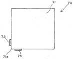
도 7은 유전체 기부 본체 측면의 세로로 연장되는 변의 양측에 1개씩 전기 공급 도체 막이 형성되어 이루어지는 안테나 장치의 수평 단면도이다.7 is a horizontal cross-sectional view of an antenna device in which electrical supply conductor films are formed one by one on both sides of a longitudinally extending side of the side of the dielectric base body.
도 7에 도시하는 안테나 장치(70)는 직사각형 형상의 유전체 기부 본체(71)를 구비하고 있고, 유전체 기부 본체(71)의 측면의, 상하 방향으로 연장되는 4개의 변 중 1개의 변(71a)의 양측에 1개씩 전기 공급 도체 막(72, 73)이 형성되어 있다. 따라서, 변(71a)에서 전기 공급 도체 막(72)까지의 거리와, 변(71a)에서 전기 공급 도체 막(73)까지의 거리를 합친 거리를, 도 5, 도 6에 도시하는 전기 공급 도체 막 사이의 거리와 동일하게 설계하였을 때, 도 7에 도시하는 안테나 장치쪽이, 도 5, 도 6에 도시하는 안테나 장치와 비교하여, 2개의 전기 공급 도체 막 사이의 거리가 가깝게 되어, 상술한 수학식 (3)이 도시하는 유효 유전율 εreff가 커진다. 따라서, 도 5, 도 6의 안테나 장치와 도 7의 안테나 장치를 비교하면, 상술한 수학식 (2)중의 W의 값이 같은 경우, 전기 공급 도체 막의 임피던스(Z)를 모두 Z=Z1로 조정하고자 하면, 도 7의 안테나 장치쪽이 유효 유전율 εreff가 큼에 따라, 수학식 (1)에 도시하는 k의 값도 크게 할 필요가 있다. 이 k의 값을 크게 한다는 것은, 도 7의 안테나 장치의 전기 공급 도체 막의 폭(S)을, 도 5, 도 6의 안테나 장치의 전기 공급 도체 막의 폭(S)보다 좁히는 것이 된다. 따라서, 도 7의 안테나 장치는 도 5, 도 6의 안테나 장치보다 전기 공급 도체 막의 폭이 좁더라도 임피던스를 정합시킬 수 있다. 즉, 본 발명의 제 8 안테나 장치를 이용하면, 전기 공급 도체 막의 갭폭이 넓더라도, 방사 도체 막의 임피던스와 전기 공급 도체 막의 임피던스를 정합시킬 수 있다.The
또한, 본 발명의 제 8 안테나 장치는, 유전체 기부 본체의 상면에 루프 형상의 방사 도체 막이 형성되어 있기 때문에, 1파장 루프 안테나 구조를 가지며, 이 방사 도체 막으로부터 방출되는 전자파는, 이 방사 도체 막을 포함하는 평면에 수직인 방향으로 최대 이득의 전자파이다. 또한, 유전체 기부 본체에는, 그 하면에 접지 도체 막이 형성되어 있기 때문에, 방사 도체 막으로부터 방출된 전자파 중 접지 도체 막으로 향하는 전자파는 접지 도체 막에서 반서된다. 즉, 안테나 장치로부터는 방사 도체 막을 포함하는 평면에 수직이면서, 또한 접지 도체 막으로부터 방사 도체 막으로 향하는 방향으로 최대 이득의 전자파가 방사된다. 따라서, 본 발명의 제 8 안테나 장치를, 예컨대 휴대 전화에 부착하는 경우, 사람이 휴대 전화를 사용할 때 접지 도체 막이 인체와 방사 도체 막 사이에 위치하도록 부착하면, 인체측에는 전자파가 방사되지 않고, 방사되는 전자파는 접지 도체 막으로부터 방사 도체 막으로 향하는 방향으로 최대 이득이면서, 효율적으로 통신에 사용된다.In addition, the eighth antenna device of the present invention has a one-wavelength loop antenna structure because a loop-shaped radiation conductor film is formed on the upper surface of the dielectric base body, and electromagnetic waves emitted from the radiation conductor film are used to radiate the radiation conductor film. It is the electromagnetic wave of the maximum gain in the direction perpendicular to the containing plane. In addition, since the ground conductor film is formed on the bottom surface of the dielectric base body, electromagnetic waves directed to the ground conductor film of the electromagnetic waves emitted from the radiation conductor film are countered by the ground conductor film. That is, the electromagnetic wave of the maximum gain is radiated from the antenna device in the direction perpendicular to the plane including the radiation conductor film and from the ground conductor film to the radiation conductor film. Therefore, when the eighth antenna device of the present invention is attached to, for example, a mobile phone, if a person attaches the ground conductor film to be located between the human body and the radiation conductor film when using the mobile phone, electromagnetic waves are not radiated to the human body side, The electromagnetic waves to be used are efficiently used for communication with maximum gain in the direction from the ground conductor film to the radiation conductor film.
또한, 본 발명의 제 8 안테나 장치는, 방사 도체 막을 형성하는 데 있어서, 유전체 기부 본체에 관통 구멍을 형성하는 것이 불필요하여, 제조 비용의 절감을 도모할 수 있다.In addition, in the eighth antenna device of the present invention, it is unnecessary to form through holes in the dielectric base body in forming the radiation conductor film, so that the manufacturing cost can be reduced.
여기서, 본 발명의 제 8 안테나 장치의 방사 도체 막이 이 방사 도체 막의, 상기 2개의 전기 공급 도체 막과의 접속점끼리의 사이가 전기적으로 개방된 개방 루프 형상의 것이어도 좋고, 또한 방사 도체 막이 띠형상(a strip-like shape)의 도체 막이 둘레에 감겨진 폐루프 형상의 것이어도 좋다.Here, the radiating conductor film of the eighth antenna device of the present invention may be an open loop shape in which the radiating conductor film is electrically open between the connection points with the two electrical supply conductor films, and the radiating conductor film is in the band shape. It may be a closed loop shape in which a conductor film of (a strip-like shape) is wound around.
이하, 본 발명의 실시예에 대하여 설명한다.EMBODIMENT OF THE INVENTION Hereinafter, the Example of this invention is described.
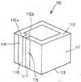
도 8은 본 발명의 실시예 1의 안테나 장치를 도시하는 사시도이고, 도 9는 그 평면도, 도 10은 그 저면도, 도 11은 그 측면도이다.Fig. 8 is a perspective view showing the antenna device according to the first embodiment of the present invention, Fig. 9 is a plan view thereof, Fig. 10 is a bottom view thereof, and Fig. 11 is a side view thereof.
도 8에 도시하는 안테나 장치(110)에는, 서로 평행한 정방형의 상면 및 하면을 갖는 직사각형 형상의 유전체 기부 본체(111)가 구비되어 있고, 그 유전체 기부 본체(111)의 상면에, 도 9에 도시하는 바와 같이 서로 근접한 2개의 단부(112a, 112b)를 가지며, 그 상면의 네 변을 따라 이들 2개의 단부(112a, 112b)를 루프 형상으로 연결하는 방사 도체 막(112)이 형성되어 있고, 이 방사 도체 막의 길이는 송신 대상 전자파의 공진 파장으로 되도록 조정되어 있다. 또한 유전체 기부 본체(111)의 하면에는, 도 10에 도시하는 바와 같이 접지 도체 막(113)이 형성되어 있고, 이 접지 도체 막(113)은 한 변의 일부가 절결된 형상을 갖고 있다. 또한 유전체 기부 본체(111)의 측면에는, 도 11에 도시하는 바와 같이 방사 도체 막(112)의 2개의 단부(112a, 112b)의 각각에 접속되어 서로 평행하게 상하 방향으로 연장되는 전기 공급 도체 막(114, 115)이 형성되어 있고, 그들 전기 공급 도체 막(114, 115) 중 한쪽의 전기 공급 도체 막(115)은 접지 도체 막(113)과도 접속되며, 이미 한쪽의 전기 공급 도체 막(114)은 유전체 기부 본체(111)의 하면에까지 도달하고 있다. 또한, 전기 공급 도체 막(114, 115)의, 접지 도체 막(113)측의 부분은 회로 기판의 표면에 장착할 때 전극인 전기 공급 전극(116, 117)으로서도 작용고 있다.The
이와 같이 구성된 안테나 장치(110)는, 방사 도체 막(112)을 구비하고 있기 때문에, 1파장 루프 안테나의 구조를 갖고 있고, 전기 공급 전극(116), 전기 공급 도체 막(114)을 경유하여 방사 도체 막(112)에 전류가 공급되어 1파장 정재파가 생성되고, 방사 도체 막(112)으로부터 유전체 기부 본체(111)의 방사 도체 막(112)이 형성되어 있는 면에 대하여 수직 방향으로 전자파가 방사되어, 접지 도체 막(113)을 향하는 전자파는 접지 도체 막(113)에서 반사한다. 즉, 안테나 장치(110)로부터는 방사 도체 막(112)을 포함하는 평면에 수직으로서, 또한 접지 도체 막(113)으로부터 방사 도체 막(112)으로 향하는 방향으로 최대 이득의 전자파가 방사된다. 따라서, 고지향성으로 고이득의 안테나 장치를 얻을 수 있고, 방사되는 전자파는 효율적으로 통신에 사용된다.Since the
또한, 유전체 기부 본체(111) 내부에 관통 구멍을 형성할 필요가 없기 때문에, 제조 비용의 절감을 도모할 수 있다.In addition, since it is not necessary to form the through hole inside the
또한, 본 발명의 실시예 1의 안테나 장치(110)는, 한쪽의 전기 공급 도체 막(115)은 접지 도체 막(113)과 접지되어 있지만, 전기 공급 도체 막은 접지되어 있지 않아도 좋다.In the
도 12는 본 발명의 실시예 2의 안테나 장치를 도시한 도면이다.12 is a diagram showing an antenna device according to a second embodiment of the present invention.
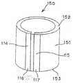
도 12에 도시한 안테나 장치(150)는, 도 8 내지 도 11에 도시한 안테나 장치(110)의 직사각형 형상의 유전체 기부 본체(111) 대신에 원주 형상의 유전체 기부 본체(151)를 채용한 것이며, 그에 따라 방사 도체 막도 원형 루프 형상의 방사 도체 막(152)이 형성되고, 접지 도체 막도 원형의 접지 도체 막(153)이 형성되어 있다.The
이와 같이, 유전체 기부 본체는 서로 평행한 상면 및 하면을 갖는 것이면 어떠한 형상이라도 좋다.Thus, the dielectric base body may have any shape as long as it has an upper surface and a lower surface parallel to each other.
도 13은 도 8 내지 도 11에 도시한 안테나 장치를 회로 기판에 탑재한 상태를 도시한 도면이다.FIG. 13 is a view showing a state in which the antenna device shown in FIGS. 8 to 11 is mounted on a circuit board.
안테나 장치(110)가 표면에 전기 공급선(161)과 접지 도체층(162)이 형성된 회로 기판(163)에, 전기 공급선(161)과 전기 공급 도체 막(114), 그리고 접지 도체층(162)과 전기 공급 도체 막(115) 각각의 한 쌍이 땜납(164)에 의해 납땜되어 있다. 이렇게 하여, 안테나 장치(110)가 회로 기판(103)에 탑재된다.The
이하에, 도 8 내지 도 11에 도시하는 안테나 장치(110)의 제조 방법에 대하여 설명한다.Hereinafter, the manufacturing method of the
우선, 유전체 기부 본체(111)의 재료를 선정한다. 이 유전체 기부 본체(111)의 재료는, 송수신되는 전자파의 주파수 대역에 있어서 비유전율이 10 내지 100정도로 안정되어 있는 재료가 바람직하며, 예컨대 Sr(Bi1/3Nb2/3)O3계 세라믹이 바람직하다. 이 재료는 송수신되는 전자파의 주파수가 6GHz일 때의 비유전율이 30이며, Q값이 1000이다.First, the material of the
다음에, 방사 도체 막(112)과 전기 공급 도체 막(114, 115)의 치수를 결정한다. 이 치수는 이하와 같이 하여 결정할 수 있다.Next, the dimensions of the
방사 도체 막(112)의 길이를 λ로 하면, λ는 이하의 수학식으로 나타낼 수 있다.When the length of the
[수학식 4][Equation 4]

단, λO : 전자파의 진공중 파장ΛO : wavelength in vacuum of electromagnetic waves
εreff : 유효 비유전율εreff : effective relative dielectric constant
또, 도 8에 도시하는 바와 같은 방사 도체 막으로부터 방사되는 전자파의 전파 방향은, 유전체 기부 본체의 방사 도체 막이 형성된 면과 수직으로 교차하는 방향이고, 유전체 기부 본체 및 공기중에 양쪽에 전계가 존재하기 때문에, 유효 비유전율 εreff는 이하의 수학식으로 나타낼 수 있다.In addition, the propagation direction of the electromagnetic waves radiated from the radiation conductor film as shown in FIG. 8 is a direction perpendicular to the plane where the radiation conductor film of the dielectric base body is formed, and an electric field exists in both the dielectric base body and the air. Therefore, the effective relative dielectric constant epsilonreff can be expressed by the following equation.
[수학식 5][Equation 5]

단, εreff : 유전체 기부 본체의 비유전율However, εreff : dielectric constant of dielectric base body
따라서, 수학식 (5)로 유효 비유전율 εreff를 구하고, 구한 εreff를 수학식(4)에 대입함으로써 λ를 구할 수 있다.Therefore, λ can be obtained by obtaining the effective relative dielectric constant epsilonreff from equation (5) and substituting the obtained epsilonreff into equation (4).
전자파의 공진 주파수를 1.9GHz로 하면, λ=40.11mm로 되어, 도 8에 도시하는 바와 같이 방사 도체 막(112)을 형성하기 위해서는, 방사 도체 막(112)의 한 변의 길이를 10.03mm로 하면 좋다. 또한, 1파장 루프 안테나의 임피던스는, 일반적으로는 100Ω 이상의 고임피던스이지만, 방사 도체 막의 폭이나 2개의 단부의 간격을 조정함으로써 임피던스를 저하시켜 전기 공급 효율을 향상시킬 수 있다. 예컨대, 임피던스를 50Ω로 하기 위해서는, 방사 도체 막(112)의 폭을 2mm로 하고, 2개의 단부(112a, 112b)의 간격을 1mm로 하면 좋다.When the resonance frequency of the electromagnetic wave is 1.9 GHz, λ = 40.11 mm, and as shown in FIG. 8, when one side of the
또한, 전기 공급 도체 막의 폭이나 전기 공급 도체끼리의 간격을 조정함으로써 소망하는 전송 임피던스를 얻을 수 있는 것이, 『C.P.Wen : "Coplanar Waveguide : A Surface Strip Transmission Line Suitable for Nonreciprocal Gyromagnetic Device Applications" , IEEE Trans. MTT, Vo1. MTT-17, No. 12, Dec. 1969』에 보고되어 있다. 여기서는 전송 임피던스를 50Ω로 하기 위해서, 전기 공급 도체 막(114, 115)의 폭을 3.09mm로 하고, 전기 공급 도체 막의 간격은 1mm로 한다.In addition, it is possible to obtain a desired transmission impedance by adjusting the width of the electric supply conductor film and the spacing between the electric supply conductors, as described in "CPWen:" Coplanar Waveguide: A Surface Strip Transmission Line Suitable for Nonreciprocal Gyromagnetic Device Applications ", IEEE Trans. . MTT, Vo1. MTT-17, No. 12, Dec. 1969. In this case, the width of the electrical
다음에, 이와 같이 치수의 결정된 방사 도체 막(112)으로부터, 유전체 기부 본체(111)의 치수를, 길이와 폭을 모두 12.03mm로 하고, 두께를 1.9GHz의 공진 주파수를 갖는 전자파의 파장의 유전체 기부 본체(111) 내에서의 1/4 파장에 상당하는 7.21mm로 하여 유전체 기부 본체(111)를 제작한다.Next, from the thus-determined
다음에, 상술한 치수를 갖는 방사 도체 막(112) 및 전기 공급 도체 막(114, 115) 및 접지 도체 막(113)의 패턴을 후막 인쇄법에 의해 구리 페이스트(paste)를 이용하여 인쇄하고, 환원 분위기중에서 소성(燒性)한다.Next, the patterns of the
이러한 제조 과정을 거침으로써, 도 8에 도시하는 안테나 장치(110)가 제조된다.By going through such a manufacturing process, the
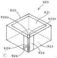
도 14는 본 발명의 실시예 3의 안테나 장치를 도시하는 사시도이고, 도 15는 그 평면도, 도 16은 그 저면도, 도 17은 그 측면도이다.Fig. 14 is a perspective view showing the antenna device according to the third embodiment of the present invention, Fig. 15 is a plan view thereof, Fig. 16 is a bottom view thereof, and Fig. 17 is a side view thereof.
도 14에 도시하는 안테나 장치(210)는 유전체 기부 본체(211)를 구비하고 있고, 이 유전체 기부 본체(211)는 정방형의 서로 평행한 상측 평면 및 하측 평면을 가짐과 동시에, 상측 평면 및 하측 평면에 대하여 수직 방향으로 연장되는 관통 구멍(212)을 갖고 있다. 이 유전체 기부 본체(211)의 두께는, 송신 대상 전자파의 공진 파장의 유전체 기부 본체(211)내에서의 1/4 파장에 상당하도록 조정되어 있고, 이 관통 구멍(212)에 단극 도체(213)가 충진됨으로써 1/4 파장 단극 안테나 구조를 갖고 있다. 유전체 기부 본체(211)의 상면에는 도 15에 도시하는 바와 같이 서로 근접한 2개의 단부(214a, 214b)를 가지며, 그 상면의 네 변을 따라 이들 2개의 단부(214a, 214b)를 루프 형상으로 연결하는 막형상의 루프 도체(214)가 형성되어 있다. 이 루프 도체(214)의 길이는 송신 대상 전자파의 공진 파장이 되도록 조정되어 있다. 또한 이 상면에는, 루프 도체(214)의 단부(214b)가 단극 도체(213)에 접속되도록 결합선(215)이 형성되어 있다. 또한 유전체 기부 본체(211)의 하면에는, 도 16에 도시하는 바와 같이 단극 도체(213)의 단부를 둘러싸도록 채널 형상으로 넓어지는 막형상의 접지 도체(216)가 형성되어 있다. 또한 이 하면에는, 한쪽 단부가 단극 도체(213)에 접속되고, 접지 도체(216)와의 사이에 동일 폭의 갭(231, 232, 233)을 갖는, 접지 도체(216)와 함께 공평면 선로를 형성하는 신호선(217)이 형성되어 있다. 또한, 유전체 기부 본체(211)의 측면에는, 도 17에 도시하는 바와 같이 전기 공급 단자(218)가 형성되고, 이 전기 공급 단자(218)는 도 14에 도시하는 바와 같이 신호선(217)에 접속되어 있다. 또한, 이 전기 공급 단자(218)가 형성된 측면과 동일한 측면에는, 전기 공급 단자(218)를 사이에 두도록 접지 단자(219, 220)가 형성되고, 이 접지 단자(219, 220)는 도 14에 도시하는 바와 같이 접지 도체(216)에 접속되어 있다.The
이와 같이 구성된 안테나 장치(210)는, 1파장 루프 안테나의 구조를 갖는 막 형상의 루프 도체(214)를 구비하고 있고, 또한 1/4 파장 단극 안테나의 구조를 갖는 단극 도체(213)도 구비하고 있다. 따라서, 전기 공급 단자(218)를 경유하여 루프 도체(214)에 전류를 공급하면, 루프 도체(214)로부터는 유전체 기부 본체(211)의 루프 도체(214)가 형성되어 있는 면에 수직으로 전자파가 방사되고, 접지 도체(216)로 향하는 전자파는 접지 도체(216)로 반사한다 한편, 단극 도체(213)로부터는 유전체 기부 본체(211)의 루프 도체(214)가 형성되어 있는 면과 평행하게 최대 이득의 전자파가 방사된다. 따라서, 안테나 장치(210)를, 예컨대 휴대 전화에 부착하는 경우, 사람이 휴대 전화를 사용할 때에 접지 도체가 인체와 루프 도체 사이에 위치하도록 부착하면, 인체측에는 전자파가 방사되지 않고, 인체측을 제외한 다른 방향으로 전자파가 효율적으로 방사된다.The
또한, 안테나 장치(210)는 접지 도체(216)와의 사이에서 공평면 선로를 형성하는 신호선(217)을 구비하는 것이며, 신호선(217)의 폭이나 신호선(217)과 접지 도체(216)와의 갭폭이 조정된 안테나 장치(210)를 제조함으로써 소망하는 선로 임피던스를 얻는다. 또한, 그 안테나 장치(210)는 전기 공급 단자(218) 및 접지 단자(219, 220)가 형성되어 있기 때문에, 납땜 등에 의해 회로 기판에 용이하게 장착된다.In addition, the
도 18은 본 발명의 실시예 4의 안테나 장치를 도시하는 측면도이다.Fig. 18 is a side view showing the antenna device of Embodiment 4 of the present invention.
이 도 18에 도시하는 실시예 4에 있어서, 도 14 내지 도 17에 도시하는 실시예 3의 요소와 대응하는 요소에는, 동일한 부호를 붙여 도시한다.In Example 4 shown in this FIG. 18, the element corresponding to the element of Example 3 shown to FIG. 14 thru | or 17 is attached | subjected and shown with the same code | symbol.
이 도 18에 도시하는 안테나 장치(250)를 구성하는 유전체 기부 본체(211)의 상면에는, 도 14 내지 도 17에 도시하는 안테나 장치(210)의 상면(도 15 참조)과 동일한 루프 도체(214) 및 결합선(215)이 형성되어 있고, 또한 유전체 기부 본체(211)의 관통 구멍(212)에는 단극 도체(213)가 충진되어 있다. 또한, 이 유전체 기부 본체(211)의 하면의, 단극 도체(213)의 하단을 제외한 부분에는 접지 도체(216)가 확장되어 있다.On the upper surface of the dielectric base body 211 constituting the antenna device 250 shown in FIG. 18, the
또한, 이 안테나 장치(250)에는 유전체 기부 본체(211)의 하면측에 동축 커넥터(253)가 고정되어 있다. 이 동축 커넥터(253)는 중심 도체(251)와 접지 도체(252)를 갖고, 중심 도체(251)는 유전체 기부 본체(211)의 관통 구멍(212)에 삽입되어 단극 도체(213)에 접속되어 있으며, 접지 도체(252)는 판형상으로 확장되어 유전체 기부 본체(211)의 하면에 형성된 접지 도체(216)에 접속되어 있다.In addition, a coaxial connector 253 is fixed to the antenna device 250 on the lower surface side of the dielectric base body 211. The coaxial connector 253 has a center conductor 251 and a ground conductor 252, and the center conductor 251 is inserted into the through hole 212 of the dielectric base body 211 and connected to the
이 안테나 장치(250)는 동축 커넥터(253)를 구비하고 있기 때문에, 이 동축 커넥터(253)에 결합되는 동축 케이블(도시하지 않음)을 경유하여 회로 기판 등에 접속된다.Since the antenna device 250 includes a coaxial connector 253, it is connected to a circuit board or the like via a coaxial cable (not shown) coupled to the coaxial connector 253.
이하, 도 14 내지 도 17에 도시하는 안테나 장치(210)를 제조한 과정에 대하여, 도 14, 도 19, 도 20, 도 21을 이용하여 설명한다. 도 19, 도 20, 도 21은 각각 유전체 기부 본체의 상면, 하면, 측면에 인쇄되는 패턴의 치수를 도시한다. 그후 안테나 장치(210)의 이득을 측정하여 얻어진 결과에 대하여 설명한다.Hereinafter, the process of manufacturing the
우선, 유전체 기부 본체(211)의 재료를 선정하였다. 이 유전체 기부 본체(211)의 재료로서는, 송수신되는 전자파의 주파수 대역에 있어서 비유전율이 10 내지 100정도로 안정되어 있는 재료가 바람직하고, 여기서는, Sr(Ni1/3Nb2/3)O3계 세라믹을 선정하였다. 이 재료는 송수신되는 전자파의 주파수가 3.8GHz일 때의 비유전율이 31이고, Q값은 1800이다.First, the material of the dielectric base body 211 was selected. As the material of the dielectric base body 211, a material having a stable relative dielectric constant of about 10 to 100 in the frequency band of the electromagnetic wave to be transmitted and received is preferable, and here, Sr (Ni1/3 Nb2/3 ) O3 system Ceramic was selected. This material has a relative dielectric constant of 31 and a Q value of 1800 when the frequency of electromagnetic waves transmitted and received is 3.8 GHz.
다음에, 막형상의 루프 도체(214)의 치수, 신호선(217)의 치수 및 신호선(217)과 접지 도체(216)와의 갭(231, 232, 233)의 폭을 결정하였다. 이들의 값은 아래와 같이 하여 결정하였다.Next, the dimensions of the film-shaped
루프 도체(214)의 길이를 λ로 하면, 이 λ는 상술한 수학식 (4)로 나타낼 수 있다. 이 수학식 (4)를 이하에 나타낸다.When the length of the
[수학식 5a]Equation 5a

단, λO : 전자파의 진공중 파장ΛO : wavelength in vacuum of electromagnetic waves
εreff : 유효 비유전율εreff : effective relative dielectric constant
또, 유효 비유전율 εreff는 도 14에 도시하는 바와 같은 막형상의 루프 도체(214)로부터 방사되는 전자파가, 유전체 기부 본체(211)의 막형상의 루프 도체(214)가 형성된 면에 수직으로 전파하여, 루프 도체(214)의 내측 및 외측에 전계가 발생하는 것을 고려하면, 이하의 수학식으로 나타낼 수 있다.In addition, the effective relative dielectric constant εreff is that the electromagnetic wave emitted from the film-shaped
[수학식 6][Equation 6]
εreff = (εr+3)/4εreff = (εr +3) / 4
단, εreff : 유전체 기부 본체의 비유전율However, εreff : dielectric constant of dielectric base body
따라서, 수학식 (6)으로 유효 비유전율 εreff를 구하고, 이 구한 εreff를 수학식 (5a)에 대입함으로써 λ를 구할 수 있다.Therefore, λ can be obtained by obtaining the effective relative dielectric constant epsilonreff from equation (6) and substituting the obtained epsilonreff into equation (5a).
여기서는, 전자파의 공진 주파수를 1.9GHz로 하였기 때문에, λ=54.11mm으로 결정하고, 도 14에 도시하는 바와 같은 루프 도체(214)를 형성하기 위해 도 19에 도시하는 바와 같이 루프 도체(214)의 한 변의 길이를 13.54mm로 결정하였다. 여기서, 도 19에 도시하는 파선은 루프 도체(214)의 각 변의 중심선을 도시한다. 또한, 1파장 루프 안테나의 임피던스는, 일반적으로는 100Ω 이상의 고임피던스이지만, 루프 도체의 폭이나 루프 도체의 2개 단부의 간격을 조정함으로써 임피던스를 저하시켜 전기 공급 효율을 향상시킬 수 있다. 여기서는, 임피던스를 50Ω로 하기 위해서, 도 19에 도시하는 바와 같이 루프 도체(214)의 폭을 2mm, 2개의 단부(214a, 214b)의 간격을 1mm로 결정하였다. 또한, 도 14에 도시하는 바와 같이 신호선과 접지 도체와는 공평면 선로를 형성하고 있기 때문에, 신호선의 폭이나 신호선과 접지 도체와의 갭폭을 조정함으로써 선로 임피던스를 조정할 수 있고, 여기서는 선로 임피던스를 50Ω로 하기 위해서, 도 20에 도시하는 바와 같이 신호선의 폭을 1mm, 갭(231, 232, 233)의 폭을 모두 3.02mm로 결정하였다.In this case, since the resonance frequency of the electromagnetic wave is 1.9 GHz, it is determined that λ = 54.11 mm and the
다음에, 이와 같이 결정된 루프 도체(214)의 치수로부터, 유전체 기부 본체(211)의 길이 및 폭을 모두 15.54mm로 결정하고, 유전체 기부 본체(211)의 두께를 1.9GHz의 공진 주파수를 갖는 전자파의 파장의 유전체 기부 본체(211)내에서의 1/4 파장에 상당하는 7.09mm로 결정하여 상술한 치수를 가짐과 동시에, 유전체 기부 본체의 두께 방향으로 직경 1mm의 관통 구멍(212)을 갖는 유전체 기부 본체(211)를 제조하였다.Next, from the dimensions of the
다음에, 유전체 기부 본체(211)에 막형상의 루프 도체(214), 신호선(218), 결합선(215), 접지 도체(216), 전기 공급 단자(218) 및 접지 단자(219, 220) 각각의 패턴을 구리 페이스트를 이용하여 후막 인쇄법(thick film printing process)에 의해 인쇄하였다. 막형상의 루프 도체는 상술한 치수를 갖도록 인쇄하고, 그 밖에 관해서는, 결합선(215)은 도 19에 도시하는 바와 같이 폭 1mm, 접지 도체(216)는 도 20에 도시하는 바와 같이 폭 4 25mm, 전기 공급 단자(218)는 도 21에 도시하는 바와 같이 폭, 길이를 각각 1mm, 접지 단자(219, 220)는 도 21에 도시하는 바와 같이 폭, 길이를 각각 1mm, 4.25mm의 치수를 갖도록 인쇄하였다. 또한, 유전체 기부 본체(211)의 관통 구멍(212)에는 구리 페이스트를 충진하였다.Next, the film-shaped
다음에, 상술한 바와 같이 구리 페이스트가 인쇄, 충진된 유전체 기부 본체(211)를 환원 분위기속에서 소성하였다.Next, as described above, the dielectric base body 211 on which the copper paste was printed and filled was fired in a reducing atmosphere.
이렇게 하여, 도 14에 도시하는 안테나 장치(210)를 제조하였다.In this way, the
다음에, 상술한 바와 같이 하여 제조된 안테나 장치(210)의 이득 특성에 대하여 도 22, 도 23을 이용하여 설명한다. 여기서는, 안테나 장치(210)의 이득 특성으로서, 도 22에 도시한 바와 같이 안테나 장치(210)의 전기 공급 단자(218), 접지 단자(219, 220)가 형성되어 있는 측면에 평행하면서, 또한 단극 도체(213)를 포함하는 면(291)내에서의 이득 특성을 구하였다. 또한, 이 도면에 도시하는 X축, Y축, Z축은 서로 90도로 교차하고, X축은 면(291)에 포함되고, 또한 루프 도체(214)의 루프면에 평행한 축이고, Y축은 면(291)에 대하여 수직인 축이며, Z축은 면(291)에 포함되고, 또한 단극 도체(213)가 연장되는 방향과 동일 방향의 축이다. 또한 화살표(W)는, X축, Y축, Z축과의 교점을 시점(始点)으로 하여 면(291)에 포함되는 화살표이고, 각 θ는, 화살표(W)와 Z축이 이루는 각이다. 이하에 설명하는 도 23에 도시하는 X축, Z축 및 각 θ는, 각각 도 22에 도시하는 X축, Z축 및 각 θ에 대응한다. 또한, 도 23의 중심으로부터 지면에 대하여 수직이면서, 또한 지면으로부터 나오는 방향이 도 22에 도시하는 Y축에 대응한다.Next, the gain characteristics of the
도 23은 안테나 장치의 이득 특성을 도시한 도면이고, 실선은 상술한 제조 과정을 거쳐 제조된, 도 14에 도시하는 안테나 장치(210)의, 도 22에 도시하는 면(291)내에 있어서 0°≤θ≤360°의 범위에서 화살표(W)가 나타내는 방향의 이득을 도시하고, 파선은 도 14에 도시하는 안테나 장치(210)가 갖는 1파장 루프 안테나 구조만을 구비한 안테나 장치의, 도 22에 도시하는 0°≤θ≤360°의 범위에서 화살표(W)가 나타내는 방향과 동일 방향의 이득을 나타낸다.FIG. 23 is a diagram showing gain characteristics of the antenna device, and the solid line is 0 ° in the
도 23으로부터, 어느 안테나 장치에 있어서도 θ=0°일 때에 최대 이득 26dB을 나타내지만, θ가 30° 내지 90° 또는 270° 내지 330°의 범위에 있어서는, 도 14에 도시하는 안테나 장치쪽이 이득이 높고, 특히 θ가 270° 내지 300°의 범위에 있어서는 루프 안테나 구조만을 구비한 안테나 장치보다도 5dB 이상 이득이 향상되어 있다.23 shows a maximum gain of 26 dB when any antenna device is θ = 0 °. However, when θ is in a range of 30 ° to 90 ° or 270 ° to 330 °, the antenna device shown in FIG. 14 is a gain. In this high range, especially in the range of 270 ° to 300 °, the gain is improved by 5 dB or more compared to the antenna device having only the loop antenna structure.
이와 같이, 도 14에 도시하는 안테나 장치(210)는 루프 안테나 구조만을 구비한 안테나 장치보다 높은 이득이 얻어지는 것을 알 수 있다.As described above, it can be seen that the
도 24는 본 발명의 실시예 5의 안테나 장치를 도시하는 사시도이고, 도 25는 그 저면도이다.24 is a perspective view showing an antenna device according to a fifth embodiment of the present invention, and FIG. 25 is a bottom view thereof.
도 24에 도시한 안테나 장치(310)는 정방형의 상면 및 정방형의 하면을 갖는 직사각형 형상의 유전체 기부 본체(311)를 구비하고 있고, 이 유전체 기부 본체(311)의 하면에는 도 25에 도시하는 바와 같이 면형상으로 넓어지는 접지 도체 막(312)이 형성되어 있으며, 이 접지 도체 막(312)은 한 변의 일부가 절결된 형상을 갖고 있다. 또한, 이 유전체 기부 본체(311)의 측면에는 도 24에 도시하는 바와 같이 좌우에 근접하는 2개의 단부(313a, 313b)를 가지며, 유전체 기부 본체(311)의 상면의 네 변을 따라 측면을 일주하여 이들 2개의 단부(313a, 313b)를 연결하는 방사 도체 막(313)이 형성되어 있다. 이 방사 도체 막(313)의 길이는 송신 대상 전자파의 공진 파장과 동일한 길이로 조정되어 있다. 또한, 유전체 기부 본체(311)의 측면에는 서로 평행하게 상하 방향으로 연장되며, 1개가 방사 도체 막(313)의 2개의 단부(313a, 313b) 중의 한쪽 단부(313a)에 접속되고, 다른 1개가 단부(313b)에 접속되는 2개의 전기 공급 도체 막(314, 315)이 형성되어 있고, 전기 공급 도체 막(315)은 접지 도체 막(312)과 접속되며, 전기 공급 도체 막(314)은 도 25에 도시하는 바와 같이 유전체 기부 본체(311)의 하면에까지 도달하고 있다. 또한, 전기 공급 도체 막(314, 315)의 접지 도체 막(312)측은 회로 기판의 표면에 장착할 때 전극인 전기 공급 전극(316, 317)으로서도 작용하고 있다.The
이와 같이 구성된 안테나 장치(310)는 1파장 루프 안테나의 구조를 갖는 방사 도체 막(313)을 구비하고 있기 때문에, 전기 공급 전극(316)을 경유하여 방사 도체 막(313)에 전류를 공급하면, 방사 도체 막(313)으로부터는 유전체 기부 본체(311)의 상면에 수직하게 최대 이득의 전자파가 방사되고, 접지 도체 막(312)으로 향하는 전자파는 이 접지 도체 막(312)에서 반사된다. 즉, 안테나 징치(310)로부터는 방사 도체 막(313)을 포함하는 평면에 수직이면서, 또한 접지 도체 막(312)으로부터 방사 도체 막(313)으로 향하는 방향으로 최대 이득의 전자파가 방사된다. 따라서, 고이득으로, 방사되는 전자파가 효율적으로 통신에 사용되는 안테나 장치를 얻을 수 있다.Since the
또한, 유전체 기부 본체(311)에 관통 구멍을 형성할 필요가 없으므로 제조 비용의 절감을 도모할 수 있다.In addition, since it is not necessary to form the through hole in the
이하에, 도 24, 도 25에 도시한 구조의 안테나 장치(310)의 제조 방법에 대하여, 도 26에 도시하는 유전체 기부 본체, 방사 도체 막 및 전기 공급 도체 막의 치수를 나타낸 도면을 이용하여 설명한다.Hereinafter, the manufacturing method of the
우선, 유전체 기부 본체(311)의 재료를 선정한다. 이 유전체 기부 본체(311)의 재료는, 송수신되는 전자파의 주파수 대역에 있어서 비유전율이 10 내지 100정도로 안정되어 있는 재료가 바람직하며, 예컨대 Sr(Ni1/3Nb2/3)O3계 세라믹이 바람직하다. 이 재료는 송수신되는 전자파의 주파수가 4GHz일 때의 비유전율이 31이고, Q값이 1000이다.First, the material of the
다음에, 방사 도체 막(313), 전기 공급 도체 막(314, 315) 및 유전체 기부 본체(311)의 치수를 결정한다. 이들 치수는 아래와 같이 하여 결정할 수 있다.Next, the dimensions of the
방사 도체 막(313)의 길이를 λ로 하면, 이 λ는 상술한 수학식 (4)로 나타낼 수 있다. 이하에 이 수학식 (4)를 나타낸다.When the length of the
[수학식 7][Equation 7]

단, λO : 전자파의 진공중 파장ΛO : wavelength in vacuum of electromagnetic waves
εreff : 유효 비유전율εreff : effective relative dielectric constant
또, 유효 비유전율 εreff는 도 26에 도시하는 바와 같은 방사 도체 막(313)으로부터 방사되는 전자파가, 유전체 기부 본체(311)의 상면에 수직으로 전파하여, 방사 도체 막(313)의 내측 및 외측에 전계가 발생하는 것을 고려하면, 이하의 수학식으로 나타낼 수 있다.In addition, the effective relative dielectric constant εreff is that the electromagnetic waves radiated from the radiating
[수학식 8][Equation 8]
εreff = (εr+3)/4εreff = (εr +3) / 4
단, εreff : 유전체 기부 본체의 비유전율However, εreff : dielectric constant of dielectric base body
따라서, 수학식 (8)로 유효 비유전율 εreff를 구하고, 이 구한 εreff를 수학식 (7)에 대입함으로써 λ를 구할 수 있다.Therefore, λ can be obtained by obtaining the effective relative dielectric constant εreff from Equation (8) and substituting the obtained εreff into Equation (7).
전자파의 공진 주파수를 1.9GHz로 하면, λ=54.16mm로 되어, 도 26에 도시하는 바와 같이 유전체 기부 본체(311)의, 정방형의 상면의 네 변에 따른 방사 도체 막을 형성하기 위해서는, 방사 도체 막(313)의 한 변의 길이를 13.54mm로 하면 좋다. 또한, 1파장 루프 안테나의 임피던스는, 일반적으로는 100Ω 이상의 고임피던스이지만, 방사 도체 막의 폭이나 방사 도체 막의 2개의 단부의 간격을 조정함으로써 임피던스를 저하시켜 전기 공급 효율을 향상시킬 수 있다. 예컨대, 임피던스를 50Ω로 하기 위해서는, 도 26에 도시한 바와 같이 방사 도체 막(313)의 폭을 2mm로 하고, 2개의 단부의 간격을 0.5mm로 하면 좋다.When the resonance frequency of the electromagnetic wave is 1.9 GHz, λ = 54.16 mm, and as shown in FIG. 26, in order to form the radiation conductor film along the four sides of the square upper surface of the
이와 같이 결정된 방사 도체 막(313)의 치수로부터, 유전체 기부 본체(311)의 길이 및 폭을 모두 13.54mm로 한다. 또한, 유전체 기부 본체(311)의 두께는, 아래와 같이 하여 결정한다.From the dimension of the
도 26에 도시한 바와 같은 루프 안테나 구조를 갖는 안테나 장치의 효율은, 방사 도체 막과, 유전체 기부 본체의 하면에 형성되는 접지 도체 막 사이의 거리가, 전자파의 공진 파장의 유전체 기부 본체 내에서의 1/4 파장에 상당하는 거리를 갖고 있는 경우에 가장 높게 된다. 따라서, 전자파의 공진 주파수를 1.9GHz로 하면, 안테나 장치의 효율을 가장 높게 하기 위해서는 방사 도체 막과 접지 도체 막 사이의 거리는 도 26에 도시하는 바와 같이 1.9GHz의 공진 주파수를 갖는 전자파의 공진 파장의, 유전체 기부 본체 내에서의 1/4 파장에 상당하는 7.09mm로 하면 좋다. 여기서, 도 26에 도시하는 일점쇄선은, 방사 도체 막(313)의 각 변의 중심을 도시한다. 또한 방사 도체 막(313)의 폭은 도 26에 도시하는 바와 같이 2mm로 하였기 때문에 유전체 기부 본체(311)의 두께를 8.09mm로 한다. 따라서, 유전체 기부 본체(311)의 길이, 폭, 두께를 각각 13.54mm, 13.54mm, 8.09mm로 한다.The efficiency of the antenna device having the loop antenna structure as shown in FIG. 26 is that the distance between the radiation conductor film and the ground conductor film formed on the lower surface of the dielectric base body is less than that in the dielectric base body of the resonant wavelength of electromagnetic waves. It becomes the highest when it has a distance corresponded to a quarter wavelength. Therefore, when the resonance frequency of the electromagnetic wave is 1.9 GHz, in order to maximize the efficiency of the antenna device, the distance between the radiation conductor film and the ground conductor film is equal to the resonance wavelength of the electromagnetic wave having the resonance frequency of 1.9 GHz as shown in FIG. It is good to set it to 7.09 mm corresponding to 1/4 wavelength in a dielectric base main body. Here, the dashed-dotted line shown in FIG. 26 shows the center of each side of the
또한, 전기 공급 도체 막의 폭이나 전기 공급 도체 막끼리의 간격을 조정함으로써 소망하는 전송 임피던스를 얻을 수 있다. 여기서는 전송 임피던스를 50Ω로 하기 위해서, 도 26에 도시하는 바와 같이 전기 공급 도체 막(314, 315)의 폭을 모두 0.97mm로 하고, 전기 공급 도체 막(314, 315)끼리의 간격을 0.5mm로 한다.In addition, the desired transmission impedance can be obtained by adjusting the width of the electric supply conductor film and the distance between the electric supply conductor films. In this case, the width of the electrical
다음에, 상술하는 바와 같은 치수를 갖는 유전체 기부 본체(311)를 제작하여, 이 유전체 기부 본체(311)에, 접지 도체 막(312), 상술한 치수를 갖는 방사 도체 막(313) 및 2개의 전기 공급 도체 막(314, 315)의 패턴을 구리 페이스트를 이용하여 후막 인쇄법에 의해 인쇄하고, 환원 분위기속에서 소성한다.Next, a
이렇게 하여 안테나 장치(310)가 제조된다.In this way, the
도 27은 본 발명의 실시예 6의 안테나 장치를 도시한 도면이다.27 is a diagram showing the antenna device according to the sixth embodiment of the present invention.
도 27에 도시한 안테나 장치(340)는, 도 24, 도 25에 도시된 안테나 장치(310)의 직사각형 형상의 유전체 기부 본체(311) 대신에 원주 형상의 유전체 기부 본체(341)를 채용한 것이며, 그에 따라 방사 도체 막도 원형 루프 형상의 방사 도체 막(343)이 형성되고, 접지 도체 막도 원형의 접지 도체 막(342)이 형성되어 있다.The antenna device 340 shown in FIG. 27 employs a cylindrical dielectric base body 341 instead of the rectangular
이와 같이, 유전체 기부 본체는 원주 형상이어도 좋다.As such, the dielectric base body may have a circumferential shape.
도 28은 도 24, 도 25에 도시하는 안테나 장치를 회로 기판에 탑재한 상태를 도시한 도면이다.FIG. 28 is a diagram showing a state where the antenna device shown in FIGS. 24 and 25 is mounted on a circuit board.
회로 기판(351)의 표면에는, 전기 공급선(352)과 접지 도체층(353)이 형성되어 있고, 전기 공급선(352)과 안테나 장치(310)의 전기 공급 전극(316) 및 접지 도체층(353)과 안테나 장치(310)의 전기 공급 전극(317)이 각각 땜납(354)에 의해 접속되어 있다. 이렇게 하여 안테나 장치(310)가 회로 기판(351)에 탑재된다.An
도 29는 본 발명의 안테나 장치의 실시예 7을 도시하는 사시도이며, 도 30은 그 평면도, 도 31은 그 저면도, 도 32는 그 측면도이다.Fig. 29 is a perspective view showing Embodiment 7 of the antenna device of the present invention, Fig. 30 is a plan view thereof, Fig. 31 is a bottom view thereof, and Fig. 32 is a side view thereof.
도 29에 도시하는 안테나 장치(410)를 구성하는 직사각형 형상의 유전체 기부 본체(411)의 내부에는, 도 30에 도시하는 바와 같이 좌우에 근접하는 2개의 단부(412a, 412b)를 가지며, 수평면내를 루프 형상으로 일주하여 이들 2개의 단부(412a, 412b)를 연결하는 방사 도체 막(412)이 형성되어 있고, 이 방사 도체 막(412)의 길이는 송신 대상 전자파의 유전체 기부 본체(411)에서의 공진 파장과 동일한 길이로 조정되어 있다. 또한, 유전체 기부 본체(411)의 내부의 방사 도체 막(412)을 포함하는 평면내에는, 방사 도체 막(412)의 2개의 단부(412a, 412b)의 각각에 접속됨과 동시에 유전체 기부 본체(411)의 측면에 노출한 내부 전기 공급 도체 막(413, 414)이 형성되어 있고, 내부 전기 공급 도체 막(413, 414)은 서로의 사이에 갭(415)을 가지며, 서로의 사이에서 공평면 선로를 형성하고 있다. 또한 유전체 기부 본체(411)의 하면에는, 도 31에 도시하는 바와 같이 접지 도체 막(416)이 형성되어 있고, 이 접지 도체 막(416)은 한 변의 일부가 절결된 형상을 갖고 있다. 또한 유전체 기부 본체(411)의 측면에는, 도 32에 도시하는 바와 같이 서로의 사이에 갭(417)을 갖도록 평행하게 상하 방향으로 연장되고, 도 29에 도시하는 바와 같이 내부 전기 공급 도체 막(413, 414)의 측면에 노출한 부분 각각에 접속된, 서로의 사이에서 공평면 선로를 형성하는 측면 전기 공급 도체 막(418, 419)이 형성되어 있으며, 그들 측면 전기 공급 도체 막(418, 419) 중 한쪽의 측면 전기 공급 도체 막(419)은 접지 도체 막(416)과도 접속되고, 이미 한쪽의 측면 전기 공급 도체 막(418)은 유전체 기부 본체(411)의 하면에까지 도달하고 있다. 또한, 측면 전기 공급 도체 막(418, 419)의 접지 도체 막(416)측은, 회로 기판의 표면에 장착할때 전극인 전기 공급 전극(420, 421)으로서도 작용하고 있다.Inside the rectangular dielectric base body 411 constituting the
이와 같이 구성된 안테나 장치(410)는 1파장 루프 안테나의 구조를 갖도록 방사 도체 막(412)을 구비하고 있기 때문에, 전기 공급 전극(420)을 경유하여 방사 도체 막(412)에 전류를 공급하면, 방사 도체 막(412)으로부터는 이 방사 도체 막(412)을 포함하는 평면에 수직인 방향으로 최대 이득의 전자파가 방사되고, 접지 도체 막(416)으로 향하는 전자파는 이 접지 도체 막(416)으로 반사한다. 즉, 안테나 장치(410)로부터는 접지 도체 막(416)으로부터 방사 도체 막(412)으로 향하는 방향으로 최대 이득의 전자파가 방사된다. 따라서, 고이득으로, 방사되는 전자파가 효율적으로 통신에 사용되는 안테나 장치를 얻을 수 있다.Since the
또한, 안테나 장치(410)는 서로의 사이에서 공평면 선로를 형성하는 내부 전기 공급 도체 막(413, 414) 및 서로의 사이에서 공평면 선로를 형성하는 측면 전기 공급 도체 막(418, 419)을 구비하는 것이며, 각 내부 전기 공급 도체 막(413, 414)의 폭, 각 측면 전기 공급 도체 막(418, 419)의 폭, 내부 전기 공급 도체 막(413, 414) 사이의 갭(415)의 갭폭, 측면 전기 공급 도체 막(418, 419)의 갭(417)의 갭폭 등이 조정된 안테나 장치(410)를 제조함으로써 소망하는 전송 임피던스를 얻을 수 있다.The
또한, 안테나 장치(410)는 방사 도체 막(412)이 내부에 형성된 것이며, 소형화를 실현할 수 있다.In addition, the
또한, 안테나 장치(410)는 전기 공급 도체 막(418, 419)의 접지 도체 막(416)측이 각각 전기 공급 전극(420, 421)으로서도 작용하고 있기 때문에, 납땜 등에 의해 회로 기판에 용이하게 장착된다.In addition, since the
이하에, 도 29에 도시하는 안테나 장치(410)의 제조방법에 대하여, 도 29, 도 33, 도 34를 이용하여 설명한다. 도 33은 안테나 장치(410)의 평면도로서, 유전체 기부 본체의 길이와 폭, 방사 도체 막, 내부 전기 공급 도체 막의 치수를 도시한 도면이고, 도 34는 안테나 장치(410)의 측면도로서, 유전체 기부 본체의 두께, 측면 전기 공급 도체 막의 치수를 도시한 도면이다.Hereinafter, the manufacturing method of the
우선, 유전체 기부 본체(411)의 재료를 선정한다. 유전체 기부 본체(411)의 재료로서는, 송수신되는 전자파의 주파수 대역에 있어서, 비유전율이 10 내지 100정도로 안정되어 있는 재료가 바람직하고, 또한, 안테나 장치(410)로서는 도 29에 도시하는 바와 같이 유전체 기부 본체(411)의 내부에 방사 도체 막(412)이 형성되기 때문에, 저온에서 소성 가능한 재료가 바람직하다. 예컨대 Sr(Ni1/3Nb2/3)O3계 세라믹에 세라믹을 첨가한 재료가 바람직하다. 이 재료는, 송수신되는 전자파의 주파수가 6GHz일 때의 비유전율이 25, Q값이 1000, 소성 온도가 1000℃이다.First, the material of the dielectric base body 411 is selected. As the material of the dielectric base body 411, a material having a stable relative dielectric constant of about 10 to 100 in the frequency band of the electromagnetic wave to be transmitted and received is preferable. As the
다음에, 방사 도체 막(412), 내부 전기 공급 도체 막(413, 414), 측면 전기 공급 도체 막(418, 419) 및 유전체 기부 본체(411)의 치수를 결정한다. 이들의 치수는 아래와 같이 결정할 수 있다.Next, the dimensions of the radiating
방사 도체 막(412)의 길이를 λ로 하면, 이 λ는 상술한 수학식 (4)으로 나타낼 수 있다. 이하에, 이 수학식 (4)를 나타낸다.When the length of the
[수학식 9][Equation 9]

단, λO : 전자파의 진공중 파장ΛO : wavelength in vacuum of electromagnetic waves
εreff : 유효 비유전율εreff : effective relative dielectric constant
안테나 장치(410)에서는, 방사 도체 막(412)이 유전체 기부 본체(411)의 내부에 형성되어 있기 때문에, εreff는 유전체 기부 본체(411)의 비유전율 εr과 일치한다. 따라서, λ는 이하의 식으로 나타낼 수 있다.In the
[수학식 10][Equation 10]

전자파의 공진 주파수를 1.9GHz로 하면, λ=31.56mm로 되어, 도 33에 도시하는 것 같은 방사 도체 막(412)을 형성하기 위해서는, 방사 도체 막(412)의 한 변의 길이를 7.89mm로 하면 좋다. 여기서, 도 33에 도시하는 일점쇄선은 방사 도체 막(412)의 각 변의 중심선을 도시한다. 또한, 1파장 루프 안테나의 임피던스는 일반적으로는 100Ω 이상의 고임피던스이지만, 방사 도체 막의 폭이나 방사 도체 막의 2개의 단부의 간격을 조정함으로써 임피던스를 저하시켜 전기 공급 효율을 향상시킬 수 있다. 예컨대, 임피던스를 50Ω로 하기 위해서는, 도 33에 도시하는 바와 같이 방사 도체 막의 폭을 2mm, 2개의 단부의 간격을 0.4mm로 하면 좋다.When the resonance frequency of the electromagnetic wave is 1.9 GHz, λ = 31.56 mm, and the length of one side of the
이와 같이 치수의 결정된 방사 도체 막을, 예컨대 유전체 기부 본체(411)의 측면으로부터 방사 도체 막(412)의 바깥 둘레까지의 거리가, 도 33에 도시하는 바와 같이 1mm로 되도록 형성하기 위해서는, 유전체 기부 본체(411)의 길이 및 폭을 모두 1189mm로 하면 좋다. 또한 유전체 기부 본체의 두께는, 아래와 같이 하여 결정되는 도 29에 도시하는 바와 같은 루프 안테나 구조를 갖는 안테나 장치의 이득은, 방사 도체 막과, 유전체 기부 본체의 하면에 형성되는 접지 도체 막과의 거리가 송수신 대상 전자파의 공진 파장의 유전체 기부 본체 내에서의 1/4 파장에 상당하는 거리를 갖고 있는 경우에 가장 높게 된다. 따라서, 전자파의 공진 주파수를 1.9GHz로 하면, 안테나 장치의 이득을 가장 높게 하기 위해서는, 방사 도체 막과 접지 도체 막과의 거리는 도 34에 도시하는 바와 같이 1.9GHz의 공진 주파수를 갖는 전자파의 공진 파장의 유전체 기부 본체 내에서의 1/4 파장의 거리에 상당하는 7.89mm로 하면 좋고, 방사 도체 막(412)을 예컨대 방사 도체 막(412)으로부터 유전체 기부 본체(411)의 상면까지의 거리가 2mm가 되도록 형성하기 위해서는, 도 34에 도시하는 바와 같이 유전체 기부 본체의 두께를 9.89mm로 하면 좋다. 즉, 유전체 기부 본체(411)의 길이, 폭, 두께를 각각 11.89mm, 11.89mm, 9.89mm로 하면 좋다.In order to form the thus-determined dimension of the radiation conductor film, for example, from the side surface of the dielectric base body 411 to the outer circumference of the
또한, 내부 전기 공급 도체 막의 폭이나 내부 전기 공급 도체 막 사이의 갭의 갭폭, 또한 측면 전기 공급 도체 막의 폭이나 측면 전기 공급 도체 막 사이의 갭의 갭폭을 조정함으로써 소망하는 전송 임피던스를 얻을 수 있다. 예컨대, 전송 임피던스를 50Ω로 하기 위해서는, 도 33에 도시하는 바와 같이 내부 전기 공급 도체 막(413, 414)의 폭을 모두 0.35mm, 갭(415)의 갭폭을 0.40mm으로 하고, 도 34에 도시하는 바와 같이 측면 전기 공급 도체 막(418, 419)의 폭을 모두 1.69mm, 갭(417)의 갭폭을 0.40mm로 한다.Further, the desired transmission impedance can be obtained by adjusting the width of the internal electric supply conductor film, the gap width of the gap between the internal electric supply conductor film, and the width of the side electric supply conductor film or the gap between the side electric supply conductor film. For example, in order to set the transmission impedance to 50?, As shown in FIG. 33, the widths of the internal electric supply conductor films 413 and 414 are all 0.35 mm, and the gap width of the gap 415 is 0.40 mm, and is shown in FIG. As described above, the widths of the side electrical
다음에, 상술하는 바와 같은 치수를 갖는 유전체 기부 본체(411)의 내부에, 상술한 치수를 갖는, 방사 도체 막(412) 및 내부 전기 공급 도체 막(413, 414)의 패턴을 구리 페이스트를 이용하여 후막 인쇄법에 의해 인쇄하고, 또한, 유전체 기부 본체(411)의 측면에 상술한 치수를 갖는 측면 전기 공급 도체 막(418, 419)의 패턴을 구리 페이스트를 이용하여 후막 인쇄법에 의해 인쇄하며, 또한, 유전체 기부 본체(411)의 하면에 전기 공급 전극(420) 및 접지 도체 막(416)의 패턴을 구리 페이스트를 이용하여 후막 인쇄법에 의해 인쇄하고, 환원 분위기속에서 소성한다.Next, a copper paste is used as the pattern of the
이렇게 하여 안테나 장치(410)가 제조된다.In this way, the
도 35는 본 발명의 실시예 8의 안테나 장치를 도시한 도면이다.35 is a diagram showing the antenna device according to the eighth embodiment of the present invention.
도 35에 도시하는 안테나 장치(470)는, 도 29 내지 도 32에 도시하는 안테나 장치(410)의 직사각형 형상의 유전체 기부 본체(411) 대신에 원주 형상의 유전체 기부 본체(471)를 채용한 것이며, 그에 따라 방사 도체 막도 원형 루프 형상의 방사 도체 막(472)이 형성되며, 접지 도체 막도 원형의 접지 도체 막(476)이 형성되어 있다.The antenna device 470 shown in FIG. 35 employs a cylindrical dielectric base body 471 instead of the rectangular dielectric base body 411 of the
이와 같이, 유전체 기부 본체는 원주 형상이어도 좋다.As such, the dielectric base body may have a circumferential shape.
도 36은 도 29 내지 도 32에 도시하는 안테나 장치를 회로 기판에 탑재한 상태를 도시한 도면이다.36 is a diagram showing a state in which the antenna device shown in FIGS. 29 to 32 is mounted on a circuit board.
회로 기판(481)의 표면에는, 전기 공급선(482)과 접지 도체층(483)이 형성되어 있고, 전기 공급선(482)과 안테나 장치(410)의 전기 공급 전극(420) 및 접지 도체층(483)과 안테나 장치(410)의 전기 공급 전극(421)이 각각 땜납(484)에 의해 접속되어 있다. 이렇게 하여 안테나 장치(410)가 회로 기판(481)에 탑재된다.An
도 37은 본 발명의 실시예 9의 안테나 장치를 도시하는 사시도이고, 도 38은 그 평면도, 도 39는 그 A-A' 단면도, 도 40은 그 저면도, 도 41은 도 37에 도시하는 안테나 장치의 제 1 전기 공급 도체 막이 형성된 측면을 도시한 도면이며, 도 42는 도 37에 도시하는 안테나 장치의 제 2 전기 공급 도체 막이 형성된 측면을 도시한 도면이다.FIG. 37 is a perspective view showing the antenna device according to the ninth embodiment of the present invention, FIG. 38 is a plan view thereof, FIG. 39 is a sectional view taken along line AA ′ thereof, FIG. 40 is a bottom view thereof, and FIG. 41 is a view of the antenna device shown in FIG. 37. It is a figure which shows the side surface in which the 1st electrical supply conductor film was formed, and FIG. 42 is a figure which shows the side surface in which the 2nd electricity supply conductor film | membrane of the antenna apparatus shown in FIG. 37 was formed.
도 37에 도시하는 안테나 장치(510)는, 정방형의 상면 및 하면을 갖는 직사각형 형상의 유전체 기부 본체(511)를 구비하고 있다. 이 유전체 기부 본체(511)의 상면에는, 이 상면의 네 변에 따라 제 1 루프 방사 도체 막(513)이 형성되어 있다. 이 제 1 루프 방사 도체 막(513)은 도 38에 도시하는 바와 같이 제 1 갭(512)을 사이에 두고 마주 보는 2개의 단부(513a, 513b)가 형성되도록 이 상면내를 일주하고 있고, 이 루프의 길이는 송수신 대상 전자파의 공진 파장과 동일한 길이로 조정되어 있다. 또한, 유전체 기부 본체(511)의 내부에는, 정방형 형상으로 수평면내를 한번 감는 제 2 루프 방사 도체 막(515)이 형성되어 있다. 이 제 2 루프 방사 도체 막(515)은, 도 39에 도시하는 바와 같이 제 2 갭(514)을 사이에 두고 마주보는 2개의 단부(515a, 515b)가 형성되도록 수평면내를 일주하고 있으며, 이 제 2 루프 방사 도체 막(515)의 루프에 대한 제 2 갭(514)의 방향은 도 37에 도시하는 바와 같이 제 1 루프 방사 도체 막(513)의 루프에 대한 제 1 갭(512)의 방향에 비해 수평면내에서 90도 다른 방향으로 조정되어 있다. 또한, 이 제 2 루프 방사 도체 막(515)의 루프의 길이는 송수신 대상의 전자파의 유전체 기부 본체(511)내에서의 공진 파장과 동일한 길이로 조정되어 있다. 또한 유전체 기부 본체(511)의 하면에는, 도 40에 도시하는 바와 같이 접지 도체 막(516)이 형성되어 있고, 이 접지 도체 막(516)은 네 변 중 두 변 각각의 일부가 절결된 형상을 갖고 있다. 또한 유전체 기부 본체(511)의 4개의 측면 중의 1개의 측면에는, 도 41에 도시하는 바와 같이 서로의 사이에 갭(517)을 갖는 2개의 제 1 전기 공급 도체 막(518, 519)이 형성되어 있고, 다른 측면에는 도 42에 도시하는 바와 같이 서로의 사이에 갭(520)을 갖는 2개의 제 2 전기 공급 도체 막(521, 522)이 형성되어 있다. 도 41에 도시하는 2개의 제 1 전기 공급 도체 막(518, 519)은, 도 37에 도시하는 바와 같이 제 1 루프 방사 도체 막(513)의 2개의 단부(513a, 513b)에 접속되어, 서로 평행하게 유전체 기부 본체(511)의 측면을 경유하여 연장되어 있고, 이들 2개의 전기 공급 도체 막(518, 519) 중 한쪽의 전기 공급 도체 막(519)은 접지 도체 막(516)에 접속되고, 다른쪽의 전기 공급 도체 막(518)은 유전체 기부 본체(511)의 하면에 까지 도달하고 있다. 또한, 2개의 전기 공급 도체 막(518, 519)의 접지 도체 막(516)측은, 각각 회로 기판의 표면에 장착할 때 전극인 전기 공급 전극(518a, 519a)으로서도 작용하고 있다. 한편, 도 42에 도시하는 2개의 제 2 전기 공급 도체 막(521, 522)은 제 1 전기 공급 도체 막(518, 519)과 마찬가지로, 도 37에 도시하는 바와 같이 각각 제 2 루프 방사 도체 막(515)의 2개의 단부(515a, 515b)에 접속되어 서로 평행하게 유전체 기부 본체(511)의 측면을 경유하여 연장되어 있으며, 이들 2개의 전기 공급 도체 막(521, 522) 중의 한쪽의 전기 공급 도체 막(522)은 접지 도체 막(516)에 접속되고, 다른쪽의 전기 공급 도체 막(521)은 유전체 기부 본체(511)의 하면에까지 도달하고 있다. 또한, 2개의 전기 공급 도체 막(521, 522)의 접지 도체 막(516)측은 회로 기판의 표면에 장착할 때 전극인 전기 공급 전극(521a, 522a)으로서도 작용하고 있다.The antenna device 510 illustrated in FIG. 37 includes a rectangular dielectric base body 511 having a square top and bottom surfaces. On the upper surface of the dielectric base body 511, a first loop radiation conductor film 513 is formed along four sides of the upper surface. As shown in Fig. 38, the first loop radiation conductor film 513 is circumscribed in the upper surface such that two end portions 513a and 513b facing each other with the first gap 512 are formed therebetween. The length of the loop is adjusted to the same length as the resonance wavelength of the electromagnetic wave to be transmitted and received. Further, inside the dielectric base body 511, a second loop radiating conductor film 515 is formed which winds the inside of the horizontal plane once in a square shape. As shown in Fig. 39, the second loop radiation conductor film 515 is circulated in a horizontal plane such that two end portions 515a and 515b facing each other with the second gap 514 are formed therebetween. The direction of the second gap 514 with respect to the loop of the second loop radiation conductor film 515 is the direction of the first gap 512 with respect to the loop of the first loop radiation conductor film 513 as shown in FIG. 37. Compared to the horizontal plane, it is adjusted 90 degrees in the other direction. The length of the loop of the second loop radiation conductor film 515 is adjusted to the same length as the resonance wavelength in the dielectric base body 511 of the electromagnetic wave to be transmitted and received. In addition, a ground conductor film 516 is formed on the bottom surface of the dielectric base body 511, and the ground conductor film 516 has a shape in which a part of each of two sides of the four sides is cut out. Have Further, on one side of the four sides of the dielectric base body 511, two first electric supply conductor films 518 and 519 having a gap 517 are formed between each other as shown in FIG. On the other side, as shown in FIG. 42, two second electric supply conductor films 521 and 522 having a gap 520 are formed between each other. The two first electric supply conductor films 518 and 519 shown in FIG. 41 are connected to the two ends 513a and 513b of the first loop radiating conductor film 513 as shown in FIG. Extends in parallel via the side surface of the dielectric base body 511, one of these two electrical supply conductor films 518, 519 is connected to the ground conductor film 516, The other electrical supply conductor film 518 reaches the lower surface of the dielectric base body 511. In addition, the ground conductor film 516 side of the two electricity supply conductor films 518 and 519 also functions as the electricity supply electrodes 518a and 519a which are electrodes when they are mounted on the surface of a circuit board, respectively. On the other hand, the two second electric supply conductor films 521 and 522 shown in Fig. 42 are similar to the first electric supply conductor films 518 and 519, respectively, as shown in Fig. 37, respectively. It is connected to the two ends 515a and 515b of 515 and extends in parallel with each other via the side surface of the dielectric base body 511, and the electrical supply conductor of one of these two electrical supply conductor films 521 and 522 is extended. The film 522 is connected to the ground conductor film 516, and the other electrical supply conductor film 521 reaches the lower surface of the dielectric base body 511. In addition, the ground conductor film 516 side of the two electric supply conductor films 521 and 522 also functions as the electric supply electrodes 521a and 522a serving as electrodes when mounted on the surface of the circuit board.
이와 같이 구성된 안테나 장치(510)에는, 갭의 방향이 수평면내에서 서로 90도 다른, 제 1 루프 방사 도체 막(513) 및 제 2 루프 방사 도체 막(515)이 형성되어 있기 때문에, 이들 제 1, 제 2 루프 방사 도체 막(513, 515)에 의해 수신되는 전자파의 편파 방향은 수평면내에서 서로 90도 다르다. 따라서, 이 안테나 장치(510)는 전자파가 수직 편파 또는 수평 편파의 어느 쪽이어도 전자파를 효율적으로 수신하는 것이 가능하다.Since the first loop radiation conductor film 513 and the second loop radiation conductor film 515 are formed in the antenna device 510 configured as described above, the directions of the gaps being different from each other by 90 degrees in the horizontal plane. The polarization directions of the electromagnetic waves received by the second loop radiation conductor films 513 and 515 are 90 degrees different from each other in the horizontal plane. Therefore, the antenna device 510 can efficiently receive electromagnetic waves regardless of whether the electromagnetic waves are vertically polarized or horizontally polarized.
또한, 안테나 장치(510)는 제 1 전기 공급 도체 막(518, 519)의 접지 도체 막(516)의 근방 및 제 2 전기 공급 도체 막(521, 522)의 접지 도체 막(516)의 근방이 전기 공급 전극으로서도 작용하고 있기 때문에, 납땜 등에 의해 회로 기판에 용이하게 장착된다.In addition, the antenna device 510 is provided near the ground conductor film 516 of the first electrical supply conductor films 518 and 519 and near the ground conductor film 516 of the second electrical supply conductor films 521 and 522. Since it also functions as an electrical supply electrode, it is easily attached to a circuit board by soldering etc.
또한, 이 안테나 장치(510)에서는 제 1, 제 2 루프 방사 도체 막(513, 515)이, 제 1 루프 방사 도체 막(513)의 갭의 방향과, 제 2 루프 방사 도체 막(515)의 갭의 방향이 수평면내에서 서로 90도 다른 방향으로 형성되어 있지만, 갭의 방향은 서로, 예컨대 45도 다른 방향이어도 좋고, 갭의 방향이 다르면, 1개의 안테나로 편파 방향이 다른 전자파를 수신할 수 있다.In the antenna device 510, the first and second loop radiation conductor films 513 and 515 are formed in the direction of the gap of the first loop radiation conductor film 513 and the second loop radiation conductor film 515. Although the direction of the gap is formed in a direction different from each other by 90 degrees in the horizontal plane, the direction of the gap may be different from each other, for example, 45 degrees, and if the direction of the gap is different, one antenna can receive electromagnetic waves with different polarization directions. have.
이하에, 도 37 내지 도 42에 도시한 안테나 장치(510)의 제조방법에 대하여, 도 37 및 도 43 내지 도 46을 이용하여 설명한다. 도 43은 도 37에 도시한 안테나장치(510)의 평면도로서, 유전체 기부 본체의 길이와 폭, 제 1 루프 방사 도체 막의 치수를 도시한 도면이고, 도 44는 도 37에 도시한 안테나 장치(510)의 A-A' 단면도로서, 유전체 기부 본체의 길이와 폭, 제 2 루프 방사 도체 막의 치수를 도시한 도면이며, 도 45는 안테나 장치(510)의 제 1 전기 공급 도체 막이 형성된 측면을 도시한 도면으로서, 유전체 기부 본체의 두께, 제 1 전기 공급 도체 막의 치수를 도시한 도면이고, 도 46은 안테나 장치(510)의 제 2 전기 공급 도체 막이 형성된 측면을 도시한 도면으로서, 유전체 기부 본체의 두께, 제 2 전기 공급 도체 막의 치수를 도시한 도면이다.Hereinafter, the manufacturing method of the antenna device 510 shown in FIGS. 37-42 is demonstrated using FIG. 37 and FIG. 43-46. FIG. 43 is a plan view of the antenna device 510 shown in FIG. 37, which shows the length and width of the dielectric base body and the dimensions of the first loop radiating conductor film. FIG. 44 is the antenna device 510 shown in FIG. A cross-sectional view taken along line AA ′ showing the length and width of the dielectric base body and dimensions of the second loop radiating conductor film, and FIG. 45 is a view showing the side surface of the antenna device 510 in which the first electric supply conductor film is formed. The thickness of the dielectric base body and the dimensions of the first electrical supply conductor film are shown, and FIG. 46 is a side view of the antenna device 510 in which the second electrical supply conductor film is formed. 2 is a diagram showing dimensions of an electric supply conductor film.
우선, 유전체 기부 본체(511)의 재료를 선정한다. 이 유전체 기부 본체(511)의 재료는, 송수신되는 전자파의 주파수 대역에 있어서 비유전율이 10 내지 100정도로 안정되어 있는 재료가 바람직하고, 예컨대 Sr(Ni1/3Nb2/3)O3계 세라믹이 바람직하다. 이 재료는, 송수신되는 전자파의 주파수가 3.8GHz일 때의 비유전율이 31이고, Q값이 1800이다.First, the material of the dielectric base body 511 is selected. The material of the dielectric base body 511 is preferably a material whose relative dielectric constant is stable at about 10 to 100 in the frequency band of the electromagnetic wave to be transmitted and received, for example, Sr (Ni1/3 Nb2/3 ) O3 based ceramic. This is preferred. This material has a dielectric constant of 31 and a Q value of 1800 when the frequency of electromagnetic waves transmitted and received is 3.8 GHz.
다음에, 제 1, 제 2 루프 방사 도체 막, 제 1, 제 2 전기 공급 도체 막 및 유전체 기부 본체의 치수를 결정한다. 이 치수는 아래와 같이 하여 결정할 수 있다.Next, the dimensions of the first and second loop radiating conductor films, the first and second electric supply conductor films and the dielectric base body are determined. This dimension can be determined as follows.
제 1, 제 2 루프 방사 도체 막(513, 515)의 루프의 길이를, 각각 λ1, λ2로 하면, λ1, λ2는 각각 상술한 수학식 (4)로 나타낼 수 있다. 이하에, λ1, λ2 각각을 구하는 식을 나타낸다.When the lengths of the loops of the first and second loop radiating conductor films 513 and 515 are λ1 and λ2 , respectively, λ1 and λ2 can be represented by the above equation (4). Below, the formula which calculates each of (lambda)1 and (lambda)2 is shown.
[수학식 11][Equation 11]

[수학식 12][Equation 12]

단, λO : 전자파의 진공중 파장ΛO : wavelength in vacuum of electromagnetic waves
εreff-1, εreff-2 : 유효 비유전율εreff-1 , εreff-2 : effective relative dielectric constant
여기서, 수학식 (11)에 있어서의 유효 비유전율 εreff-1은 제 1 루프 방사 도체 막(513)이 유전체 기부 본체(511)의 상면에 형성되고, 또한 제 1 루프 방사 도체 막(513)으로부터 방사되는 전자파가, 유전체 기부 본체(511)의 제 1 루프 방사 도체 막(513)이 형성된 면에 수직으로 방사되어, 제 1 루프 방사 도체 막(513)의 내측 및 외측에 전계가 발생하는 것을 고려하면, 이하의 식으로 나타낼 수 있다.Here, the effective relative dielectric constant?Reff-1 in Equation (11) is that the first loop radiation conductor film 513 is formed on the upper surface of the dielectric base body 511, and the first loop radiation conductor film 513 is also used. Electromagnetic waves radiated from the base body 511 are radiated perpendicularly to the surface on which the first loop radiating conductor film 513 is formed, so that an electric field is generated inside and outside the first loop radiating conductor film 513. In consideration, it can be represented by the following formula.
[수학식 13][Equation 13]

단, εr : 유전체 기부 본체의 비유전율However, εr : relative dielectric constant of dielectric base body
또한 수학식 (12)에 있어서의 유효 비유전율 εreff-2는 제 2 루프 방사 도체 막(515)이 유전체 기부 본체(511)의 내부에 형성되고, 또한 제 2 루프 방사 도체 막(515)으로부터 방사되는 전자파가 유전체 기부 본체(511)의 제 1 루프 방사 도체 막(513)이 형성된 면에 수직으로 방사되어, 제 2 루프 방사 도체 막(515)의 내측 및 외측에 전계가 발생하는 것을 고려하면, 이하의 식으로 나타낼 수 있다.In addition, the effective relative dielectric constant?Reff-2 in Equation (12) is that the second loop radiation conductor film 515 is formed inside the dielectric base body 511, and from the second loop radiation conductor film 515, Considering that the radiated electromagnetic waves are radiated perpendicularly to the surface where the first loop radiating conductor film 513 of the dielectric base body 511 is formed, and an electric field is generated inside and outside the second loop radiating conductor film 515. , Can be represented by the following formula.
[수학식 14][Equation 14]

단, εr : 유전체 기부 본체의 비유전율However, εr : relative dielectric constant of dielectric base body
따라서, 수학식 (13), 수학식 (14)로 구한 유효 비유전율 εreff-1, εreff-2를 각각 수학식 (11), 수학식 (12)에 대입함으로써 제 1, 제 2 루프 방사 도체 막(513, 515)의 길이 λ1, λ2를 구할 수 있다.Therefore, the first and second loop radiations are substituted by substituting the effective relative dielectric constants εreff-1 and εreff-2 obtained by the equations (13) and (14) into equations (11) and (12), respectively. The lengths λ1 and λ2 of the conductor films 513 and 515 can be obtained.
전자파의 공진 주파수를 1.9GHz로 하면, λ1=54.l6mm, λ2=39.47mm로 된다. 도 43, 도 44에 도시하는 바와 같이 제 1, 제 2 루프 방사 도체 막(513, 515)을 형성하기 위해서는, 제 1 루프 방사 도체 막(513)의 각 변의 길이를 13.54mm로 하고, 제 2 루프 방사 도체 막(515)의 각 변의 길이를 9.87mm로 하면 좋다. 여기서, 도 43, 도 44에 도시하는 일점쇄선은, 각각 제 2 루프 방사 도체 막(513, 515)의 각 변의 중심선을 도시한다. 또한, 1파장 루프 안테나의 임피던스는, 일반적으로는 100Ω 이상의 고임피던스이지만, 루프 방사 도체 막의 폭이나, 루프 방사 도체 막의 2개 단부 사이의 갭의 갭폭을 조정함으로써 임피던스를 저하시켜 전기 공급 효율을 향상시킬 수 있다. 예컨대, 임피던스를 50Ω로 하기 위해서는, 도 43, 도 44에 도시하는 바와 같이 루프 방사 도체 막의 폭을 1mm, 갭폭을 0.6mm로 하면 좋다.When the resonance frequency of the electromagnetic waves is 1.9 GHz, lambda1 = 54.16 mm and lambda2 = 39.47 mm. As shown in FIG. 43, FIG. 44, in order to form the 1st, 2nd loop radiation conductor film 513, 515, the length of each side of the 1st loop radiation conductor film 513 is 13.54 mm, and the 2nd The length of each side of the loop radiation conductor film 515 may be 9.87 mm. 43 and 44 show the centerlines of the sides of the second loop radiation conductor films 513 and 515, respectively. In addition, the impedance of a one-wavelength loop antenna is generally a high impedance of 100 Ω or more, but the impedance is lowered by adjusting the width of the loop radiation conductor film or the gap width of the gap between two ends of the loop radiation conductor film to improve electricity supply efficiency. You can. For example, in order to set the impedance to 50?, The width of the loop radiation conductor film may be 1 mm and the gap width is 0.6 mm, as shown in FIGS. 43 and 44.
이와 같이 결정된 방사 도체 막의 치수로부터, 유전체 기부 본체(511)의 길이 및 폭을, 도 43, 도 44에 도시하는 바와 같이 모두 14.54mm로 한다. 또한, 유전체 기부 본체(511)의 두께에 대해서는, 제 1 루프 방사 도체 막(513)으로부터 제 2 루프 방사 도체 막(515)까지의 거리 및 제 2 루프 방사 도체 막(515)으로부터 접지 도체 막(516)까지의 거리를, 모두 1.9GHz의 공진 주파수를 갖는 전자파의 공진 파장의 유전체 기부 본체 내에서의 1/4 파장에 상당하는 7.09mm로 하기 때문에, 유전체 기부 본체(511)의 두께는, 도 45, 도 46에 도시하는 바와 같이 14.18mm로한다.From the dimension of the radiation conductor film thus determined, the length and width of the dielectric base body 511 are set to 14.54 mm as shown in FIGS. 43 and 44. For the thickness of the dielectric base body 511, the distance from the first loop radiation conductor film 513 to the second loop radiation conductor film 515 and the ground conductor film (515) from the second loop radiation conductor film 515 ( Since the distance to 516 is set to 7.09 mm, which corresponds to a quarter wavelength in the dielectric base body of the resonant wavelength of the electromagnetic wave all having a resonance frequency of 1.9 GHz, the thickness of the dielectric base body 511 is shown in FIG. 45, it is 14.18 mm as shown in FIG.
또한, 전기 공급 도체 막의 폭이나, 전기 공급 도체 막 사이의 갭의 갭폭을 조정함으로써 소망하는 선로 임피던스를 얻을 수 있다. 예컨대, 선로 임피던스를 50Ω로 하기 위해서는, 도 45, 도 46에 도시하는 바와 같이 전기 공급 도체 막의 폭을 1.16mm, 갭폭을 0.6mm로 한다.In addition, the desired line impedance can be obtained by adjusting the width of the electric supply conductor film and the gap width of the gap between the electric supply conductor films. For example, in order to set the line impedance to 50?, The width of the electrical supply conductor film is 1.16 mm and the gap width is 0.6 mm, as shown in FIGS. 45 and 46.
다음에, 상술한 치수를 갖는 유전체 기부 본체(511)를 제작한다. 이 유전체 기부 본체(511)에는, 도 37에 도시하는 바와 같이 그 내부에도 루프 방사 도체 막이 형성되기 때문에, 길이, 폭, 두께가 각각 14.54mm, 14.54mm, 7.09mm의 유전체 소체를 2개 제작하고, 이 2개의 유전체 소체를 적층한 것을 유전체 기부 본체(511)로 한다.Next, a dielectric base body 511 having the above-described dimensions is produced. In the dielectric base body 511, as shown in Fig. 37, since a loop radiating conductor film is formed therein, two dielectric bodies each having a length, a width, and a thickness of 14.54 mm, 14.54 mm, and 7.09 mm are fabricated. The dielectric base body 511 is a laminate of these two dielectric bodies.
다음에, 제작한 2개의 유전체 소체 중 한쪽의 유전체 소체의 상면에, 도 43에 도시하는 치수를 갖는 제 1 루프 방사 도체 막(513)의 패턴을 구리 페이스트를 이용하여 후막 인쇄법에 의해 인쇄한다. 또한, 다른쪽의 유전체 소체의 상면에, 도 44에 도시하는 치수를 갖는 제 2 루프 방사 도체 막(515)의 패턴을 구리 페이스트를 이용하여 후막 인쇄법에 의해 인쇄하고, 이밖의 다른쪽의 유전체 소체의 하면에, 접지 도체 막(516)의 패턴을 구리 페이스트를 이용하여 후막 인쇄법에 의해 인쇄한다. 또한, 각 유전체 소체의 측면에, 도 45, 도 46에 도시하는 바와 같은 치수를 갖는 제 1, 제 2 전기 공급 도체 막의 패턴을 구리 페이스트를 이용하여 후막 인쇄법에 의해 인쇄한다. 그 후, 각 패턴이 인쇄된 유전체 소체를 적층하여 환원 분위기속에서 건조하여 소성한다.Next, a pattern of the first loop radiation conductor film 513 having the dimension shown in FIG. 43 is printed on the upper surface of one of the two dielectric bodies produced by thick film printing using copper paste. . Further, on the upper surface of the other dielectric body, a pattern of the second loop radiation conductor film 515 having the dimensions shown in FIG. 44 is printed by a thick film printing method using copper paste, and the other dielectric material. On the lower surface of the body, the pattern of the ground conductor film 516 is printed by thick film printing using copper paste. In addition, the patterns of the first and second electric supply conductor films having dimensions as shown in Figs. 45 and 46 are printed on the side surfaces of each dielectric body by thick film printing using copper paste. Thereafter, the dielectric bodies printed with each pattern are laminated, dried in a reducing atmosphere, and fired.
이렇게 하여 안테나 장치(510)가 제조된다.In this way, the antenna device 510 is manufactured.
도 47은, 본 발명의 실시예 10의 안테나 장치를 도시하는 사시도이다.Fig. 47 is a perspective view showing an antenna device according to a tenth embodiment of the present invention.
도 47에 도시한 안테나 장치(640)는, 정방형의 상면 및 하면을 갖는 직사각형 형상의 유전체 기부 본체(641)를 구비하고 있다. 이 유전체 기부 본체(641)의 상면에는, 이 상면의 각 변 각각에 따르도록, 4개의 방사 도체 막(642, 643, 644, 645)이 형성되어 있다. 이들 방사 도체 막(642, 643, 644, 645)은 수평방향으로 연장되어 인접하는 단부끼리가 갭(646, 647, 648, 649)을 사이에 두고 마주 봄과 동시에, 전체로서 등간격으로 4개의 갭(646, 647, 648, 649)을 형성하여 일주하고 있다. 또한, 방사 도체 막(642, 643, 644, 645) 전체의 길이는, 송수신 대상 전자파의 공진 파장과 동일한 길이로 조정되어 있다. 또한 유전체 기부 본체(641)의 하면에는 접지 도체 막(650)이 형성되어 있고, 이 접지 도체 막(650)은, 각 코너가 모두 절결된 형상을 갖고 있다. 또한 유전체 기부 본체(641)의 측면에는, 측면의 상하 방향으로 연장되는 변을 따라 전기 공급 도체 막(651, 652, 653, 654, 655, 656, 657, 658)이 형성되어 있다. 전기 공급 도체 막(651, 652)은, 방사 도체 막(642)의 각 단부에 접속되고, 전기 공급 도체 막(653, 654)은 방사 도체 막(643)의 각 단부에 접속되며, 전기 공급 도체 막(655, 656)은 방사 도체 막(644) 각 단부에 접속되고, 전기 공급 도체 막(657, 658)은, 방사 도체 막(645)의 각 단부에 접속되어 있다. 또한, 이들 각 전기 공급 도체 막(651, 652, 653, 654, 655, 656, 657, 658)의 하단측은, 각각 전기 공급 전극(651a, 652a, 653a, 654a, 655a, 656a, 657a, 658a)으로서도 작용하고 있다. 또한 유전체 기부 본체(641)의 측면의 하부에는, 2개의 접지 전극(659, 660)이 형성되고, 이들 접지 전극(659, 660)은 모두 접지 도체 막(650)에 접속되어 있다.The antenna device 640 illustrated in FIG. 47 includes a rectangular dielectric base body 641 having a square top and bottom surfaces. On the upper surface of the dielectric base body 641, four radiation conductor films 642, 643, 644, and 645 are formed so as to correspond to each side of the upper surface. These radiating conductor films 642, 643, 644, 645 extend in the horizontal direction, and adjacent ends thereof face each other with the gaps 646, 647, 648, and 649 interposed therebetween, and four at equal intervals as a whole. The gaps 646, 647, 648, and 649 are formed and are rounded. In addition, the length of the whole radiation conductor film 642, 643, 644, 645 is adjusted to the same length as the resonance wavelength of the electromagnetic wave to be transmitted / received. Further, a ground conductor film 650 is formed on the lower surface of the dielectric base body 641, and the ground conductor film 650 has a shape in which each corner is cut out. Further, on the side surface of the dielectric base body 641, an electric supply conductor film 651, 652, 653, 654, 655, 656, 657, 658 is formed along the side extending in the vertical direction of the side surface. The electrical supply conductor films 651 and 652 are connected to each end of the radiation conductor film 642, and the electrical supply conductor films 653 and 654 are connected to each end of the radiation conductor film 643. The films 655 and 656 are connected to each end of the radiation conductor film 644, and the electrical supply conductor films 657 and 658 are connected to each end of the radiation conductor film 645. In addition, the lower end side of each of these electric supply conductor films 651, 652, 653, 654, 655, 656, 657, 658 is an electric supply electrode 651a, 652a, 653a, 654a, 655a, 656a, 657a, 658a, respectively. It also works as. Further, two ground electrodes 659 and 660 are formed below the side surface of the dielectric base body 641, and both of these ground electrodes 659 and 660 are connected to the ground conductor film 650.
이와 같이 구성된 안테나 장치(640)는, 전체로서 1파장 루프 안테나 구조를 갖는 4개의 방사 도체 막(642, 643, 644, 645)이 형성되어 있기 때문에, 전기 공급 전극(656a, 657a, 652a, 653a)을 경유하여 방사 도체 막(642, 643, 644, 645)에 동일 진폭 동일 위상의 전류를 공급하면, 4개의 방사 도체 막(642, 643, 644, 645)으로부터는, 유전체 기부 본체(641)의 상면에 수직인 방향으로 지향성을 갖고, 또한 갭(649)과 갭(647)을 연결하는 직선이 연장되는 방향으로 편파한 전자파가 방사된다. 한편, 전기 공급 전극(658a, 651a, 654a, 655a)을 경유하여 방사 도체 막(642, 643, 644, 645)에 동일 진폭 동일 위상의 전류를 공급하면, 4개의 방사 도체 막(642, 643, 644, 645)으로부터는 유전체 기부 본체(641)의 상면에 수직인 방향으로 지향성을 갖고, 또한 갭(648)과 갭(646)을 연결하는 직선이 연장되는 방향으로 편파한 전자파가 방사된다.In the antenna device 640 configured as described above, since four radiation conductor films 642, 643, 644, and 645 having a one-wavelength loop antenna structure as a whole are formed, the electrical supply electrodes 656a, 657a, 652a, and 653a. When the current having the same amplitude and the same phase is supplied to the radiation conductor films 642, 643, 644, and 645 via H, the dielectric base body 641 is provided from the four radiation conductor films 642, 643, 644, and 645. Electromagnetic waves are emitted in a direction perpendicular to the upper surface of the polarized wave and polarized in a direction in which a straight line connecting the gap 649 and the gap 647 extends. On the other hand, when the current of the same amplitude and the same phase is supplied to the radiation conductor films 642, 643, 644, and 645 via the electric supply electrodes 658a, 651a, 654a, and 655a, the four radiation conductor films 642, 643, Electromagnetic waves polarized by 644 and 645 in a direction perpendicular to the upper surface of the dielectric base body 641 and polarized in a direction in which a straight line connecting the gap 648 and the gap 646 extend.
따라서, 편파 방향의 전환이 자유로운 안테나 장치를 얻을 수 있다.Therefore, the antenna device can be freely switched in the polarization direction.
또한, 이 안테나 장치(640)는 전체로서 1파장 루프 안테나 구조를 갖는 4개의 방사 도체 막(642, 643, 644, 645)이 형성되어 있기 때문에, 이 4개의 방사 도체 막(642, 643, 644, 645)으로부터 방출되는 전자파는, 이 4개의 방사 도체 막(642, 643, 644, 645)을 포함하는 평면에 수직인 방향으로 최대 이득인 전자파이다. 또한, 유전체 기부 본체(641)에는 그 하면에 접지 도체 막(650)이 형성되어 있기 때문에, 이 4개의 방사 도체 막(642, 643, 644, 645)으로부터 방출된 전자파 중 접지 도체 막(650)으로 향하는 전자파는 이 접지 도체 막(650)에서 반사된다. 즉, 안테나 장치(640)로부터는, 접지 도체 막(650)으로부터 이 4개의 방사 도체 막(642, 643, 644, 645)으로 향하는 방향으로 최대 이득의 전자파가 방사된다. 따라서, 안테나 장치(640)를, 예컨대 휴대 전화에 부착하는 경우, 사람이 휴대 전화를 사용할 때 접지 도체 막(650)이 인체와 이 4개의 방사 도체 막(642, 643, 644, 645) 사이에 위치하도록 부착하면, 인체측에는 전자파가 방사되지 않고, 전자파는 접지 도체 막(650)으로부터 4개의 방사 도체 막(642, 643, 644, 645)으로 향하는 방향으로 최대 이득으로, 효율적으로 통신에 사용된다.In addition, since the antenna device 640 has four radiation conductor films 642, 643, 644, and 645 having a one-wavelength loop antenna structure as a whole, the four radiation conductor films 642, 643, and 644 are formed. 645 is an electromagnetic wave having a maximum gain in a direction perpendicular to the plane including these four radiating conductor films 642, 643, 644, 645. In addition, since the ground conductor film 650 is formed on the bottom surface of the dielectric base body 641, the ground conductor film 650 among the electromagnetic waves emitted from these four radiation conductor films 642, 643, 644, and 645. Electromagnetic waves directed toward are reflected at the ground conductor film 650. That is, the electromagnetic wave of the maximum gain is radiated from the antenna device 640 in the direction from the ground conductor film 650 to these four radiation conductor films 642, 643, 644, and 645. Thus, when the antenna device 640 is attached to, for example, a mobile phone, when a person uses the mobile phone, the ground conductor film 650 is placed between the human body and these four radiating conductor films 642, 643, 644, 645. When attached to the body, electromagnetic waves are not radiated to the human body, and electromagnetic waves are efficiently used for communication with maximum gain in the direction from the ground conductor film 650 to the four radiation conductor films 642, 643, 644, and 645. .
이하, 도 47에 도시하는 안테나 장치(640)의 제조방법에 대하여 설명한다.Hereinafter, the manufacturing method of the antenna device 640 shown in FIG. 47 is demonstrated.
우선, 유전체 기부 본체(641)의 재료를 선정한다. 이 유전체 기부 본체(641)의 재료는, 송수신되는 전자파의 주파수 대역에 있어서 비유전율이 10 내지 100정도로 안정되어 있는 재료가 바람직하며, 예컨대 Sr(Ni1/3Nb2/3)O3계 세라믹이 바람직하다. 이 재료는, 송수신되는 전자파의 주파수가 4GHz일 때의 비유전율이 31이고, Q값이 1000이다.First, the material of the dielectric base body 641 is selected. The material of the dielectric base body 641 is preferably a material having a relative dielectric constant of about 10 to 100 in the frequency band of the electromagnetic wave to be transmitted and received. For example, Sr (Ni1/3 Nb2/3 ) O3 based ceramic This is preferred. This material has a dielectric constant of 31 and a Q value of 1000 when the frequency of electromagnetic waves transmitted and received is 4 GHz.
다음에, 방사 도체 막(642, 643, 644, 645)의 치수를 결정한다. 이 치수는 아래와 같이 하여 결정할 수 있다.Next, the dimensions of the radiation conductor films 642, 643, 644, 645 are determined. This dimension can be determined as follows.
4개의 방사 도체 막(642, 643, 644, 645)에 의해서 형성되는 루프의 길이를 λ로 하면, 이 λ는 수학식 (4)로 나타낼 수 있다. 이하에, 이 수학식 (4)를 나타낸다.When the length of the loop formed by the four radiating conductor films 642, 643, 644, and 645 is lambda, this lambda can be expressed by equation (4). The following equation (4) is shown below.
[수학식 15][Equation 15]

단, λO : 전자파의 진공중 파장ΛO : wavelength in vacuum of electromagnetic waves
εreff : 유효 비유전율εreff : effective relative dielectric constant
또, 유효 비유전율 εreff는, 도 47에 도시한 바와 같은 4개의 방사 도체 막(642, 643, 644, 645)으로부터 방사되는 전자파가, 유전체 기부 본체(641)의 4개의 방사 도체 막(642, 643, 644, 645)이 형성된 면에 수직으로 방사되어, 4개의 방사 도체 막(642, 643, 644, 645)의 내측 및 외측에 전계가 발생하는 것을 고려하면, 이하의 식으로 나타낼 수 있다.In addition, the effective relative dielectric constant εreff is that the electromagnetic waves radiated from the four radiating conductor films 642, 643, 644, and 645 as shown in FIG. 47 include four radiating conductor films 642 of the dielectric base body 641. , 643, 644, 645 is radiated perpendicularly to the plane on which the electric field is formed, and the electric field is generated inside and outside the four radiating conductor films 642, 643, 644, 645. .
[수학식 16][Equation 16]

단, εr : 유전체 기부 본체의 비유전율However, εr : relative dielectric constant of dielectric base body
따라서, 수학식 (16)으로 유효 비유전율 εreff를 구하고, 구한 εreff를 수학식 (15)에 대입함으로써 λ를 구할 수 있다.Therefore, lambda can be obtained by obtaining the effective relative dielectric constant epsilonreff from equation (16) and substituting the obtained epsilonref into equation (15).
전자파의 공진 주파수를 1.9GHz로 하면, λ=54.16mm로 되고, 도 47에 도시하는 바와 같이 방사 도체 막을 형성하기 위해서는, 각 방사 도체 막(642, 643, 644, 645)의 길이를 13.54mm로 결정하면 좋다. 또한, 1파장 루프 안테나의 임피던스는, 일반적으로는 100Ω 이상의 고임피던스이지만, 방사 도체 막의 폭이나 각 방사 도체 막의 사이의 갭의 갭폭을 조정함으로써 임피던스를 저하시켜 전기 공급 효율을 향상시킬 수 있다. 예컨대, 임피던스를 50Ω로 하기 위해서는, 각 방사 도체 막의 폭을 2mm, 각 갭의 갭폭을 0.5mm로 하면 좋다.When the resonance frequency of the electromagnetic wave is 1.9 GHz, λ = 54.16 mm, and the length of each of the radiation conductor films 642, 643, 644, and 645 is 13.54 mm in order to form the radiation conductor film as shown in FIG. You can decide. In addition, the impedance of the one-wavelength loop antenna is generally a high impedance of 100? Or more, but by adjusting the width of the radiation conductor film or the gap width of the gap between the radiation conductor films, the impedance can be lowered to improve the power supply efficiency. For example, in order to make the impedance 50Ω, the width of each radiation conductor film may be 2 mm and the gap width of each gap may be 0.5 mm.
다음에, 이와 같이 결정된 방사 도체 막의 치수로부터, 유전체 기부 본체(641)의 치수를 길이와 폭을 모두 15.54mm로 하고, 두께를 1.9GHz의 공진 주파수를 갖는 전자파의 파장의 유전체 기부 본체 내에서의 1/4 파장에 상당하는 7.09mm로 하여 유전체 기부 본체를 제작한다.Next, from the size of the radiated conductor film thus determined, the length of the dielectric base body 641 is 15.54 mm in both length and width, and the thickness is within the dielectric base body of the wavelength of electromagnetic waves having a resonance frequency of 1.9 GHz. A dielectric base body is fabricated to be 7.09 mm corresponding to 1/4 wavelength.
다음에, 전기 공급 도체 막, 접지 도체 막, 접지 전극 및 상술한 치수를 갖는 방사 도체 막의 패턴을 구리 페이스트를 이용하여 후막 인쇄법에 의해 인쇄하고, 환원 분위기속에서 소성한다.Next, the pattern of the electric supply conductor film, the ground conductor film, the ground electrode, and the radiation conductor film having the above-described dimensions is printed by thick film printing using copper paste, and fired in a reducing atmosphere.
이러한 제조 과정을 거침으로써, 도 47에 도시하는 안테나 장치(640)가 제조된다.By going through such a manufacturing process, the antenna device 640 shown in FIG. 47 is manufactured.
도 48은 도 47에 도시하는 안테나 장치를 구동하는 구동 회로를 도시한 도면이다.FIG. 48 is a view showing a driving circuit for driving the antenna device shown in FIG. 47.
구동회로(670)는 2개의 전원(671, 672)을 구비하고 있고, 전원(671)은 4개의 단자(673, 674, 675, 676)에 전류를 공급하며, 전원(672)은 4개의 단자(677, 678, 679, 680)에 전류를 공급한다.The driving circuit 670 has two power sources 671 and 672, the power source 671 supplies current to four terminals 673, 674, 675 and 676, and the power supply 672 has four terminals. Supply current to (677, 678, 679, 680).
이 구동회로(670)의 단자(673, 674, 675, 676)를 각각 도 47에 도시하는 안테나 장치(640)의 전기 공급 전극(656a, 657a, 652a, 653a)에 접속하는 한편, 구동회로(670)의 단자(677, 678, 679, 680)를 각각 안테나 장치(640)의 전기 공급 전극(658a, 651a, 654a, 655a)에 접속하면, 전원(671)을 작동시킬 때에는 전원(672)을 중지시키고, 전원(672)을 작동시킬 때에는 전원(671)을 중지시킴으로써 편파 방향의 전환이 자유로운 안테나를 얻을 수 있다.Terminals 673, 674, 675, and 676 of the drive circuit 670 are respectively connected to the electric supply electrodes 656a, 657a, 652a, and 653a of the antenna device 640 shown in FIG. When the terminals 677, 678, 679, and 680 of the 670 are connected to the electrical supply electrodes 658a, 651a, 654a, and 655a of the antenna device 640, respectively, the power source 672 is turned on when the power source 671 is operated. When the power supply 672 is stopped and the power source 672 is operated, the antenna can be freely switched in the polarization direction by stopping the power source 671.
도 49는 본 발명의 실시예 11의 안테나 장치를 도시하는 사시도이다.Fig. 49 is a perspective view showing an antenna device of
도 49에 도시하는 안테나 장치는, 도 47에 도시하는 안테나 장치(640)의 직사각형 형상의 유전체 기부 본체(641) 대신에, 원주 형상의 유전체 기부 본체(691)를 채용한 것이고, 그에 따라 방사 도체 막도 전체로서 원형 루프 형상의 방사 도체 막(692, 693, 694, 695)이 형성되고, 접지 도체 막도 원형의 접지 도체 막(696)이 형성되어 있다.The antenna device shown in FIG. 49 employs a cylindrical dielectric base body 691 instead of the rectangular dielectric base body 641 of the antenna device 640 shown in FIG. As a whole, a circular loop-shaped radiation conductor film 692, 693, 694, 695 is formed, and a ground conductor film is also formed with a circular ground conductor film 696.
이와 같이, 유전체 기부 본체는 원주 형상이어도 좋다.As such, the dielectric base body may have a circumferential shape.
도 50은 본 발명의 실시예 12의 안테나 장치를 도시하는 사시도이다.Fig. 50 is a perspective view showing an antenna device of
도 50에 도시한 안테나 장치(700)는 정방형의 상면 및 하면을 갖는 직사각형 형상의 유전체 기부 본체(701)를 구비하고 있다. 이 유전체 기부 본체(701)의 하면에는 접지 도체 막(702)이 형성되어 있고, 이 접지 도체 막(702)은 각 코너가 모두 절결된 형상을 갖고 있다. 또한,.유전체 기부 본체(701)의 측면 상부에는, 이 유전체 기부 본체(701)의 상면의 각 변을 따르도록 4개의 방사 도체 막(703)이 형성되어 있다. 이들 방사 도체 막(703)은, 수평 방향으로 연장되어 인접하는 단부끼리가 갭을 사이에 두고 마주 봄과 동시에, 전체로서 등간격으로 4개의 갭을 형성하여 일주하고 있다. 또한, 이들 4개의 방사 도체 막(703) 전체의 길이는 송수신 대상 전자파의 공진 파장과 동일한 길이로 조정되어 있다. 또한, 유전체 기부 본체(701)의 측면에는, 상하 방향으로 연장되는 각 변에 따라 8개의 전기 공급 도체 막(704)이 형성되어 있고, 각 전기 공급 도체 막(704)은 각 방사 도체 막(703)의 각 단부에 접속되어 있다. 또한, 이들 각 전기 공급 도체 막(704)의 하단측은, 전기 공급 전극(704a)으로서도 작용하고 있다. 또한 유전체 기부 본체(701)의 각 측면의 하부에는, 접지 도체 막(702)과 접속하도록 접지 전극(705)이 형성되어 있다.The
이와 같이, 방사 도체 막을 유전체 기부 본체의 측면에 형성하여도 좋다.In this manner, the radiation conductor film may be formed on the side surface of the dielectric base body.
도 51은 본 발명의 실시예 13의 안테나 장치를 도시하는 사시도이다.Fig. 51 is a perspective view showing an antenna device of Embodiment 13 of the present invention.
도 51에 도시한 안테나 장치(710)는 정방형의 상면 및 하면을 갖는 직사각형 형상의 유전체 기부 본체(711)를 구비하고 있다. 이 유전체 기부 본체(711)의 상면에는, 이 상면의 변을 따라 4개의 L자형의 방사 도체 막(712)이 형성되어 있다. 이들 4개의 방사 도체 막(712)은, 유전체 기부 본체(711)의 상면의 각 변의 중앙부에 갭을 형성하여 일주하고 있다. 이들 4개의 방사 도체 막(712) 전체의 길이는, 송수신 대상 전자파의 공진 파장과 동일한 길이로 조정되어 있다. 또한 유전체 기부 본체(711)의 하면에는, 접지 도체 막(713)이 형성되어 있고, 이 접지 도체 막(713)은 각 변의 중앙부가 절결된 형상을 갖고 있다. 또한 유전체 기부 본체(711)의 측면에는, 상하 방향으로 연장되어 있는 8개의 전기 공급 도체 막(714)이 형성되어 있고, 각 전기 공급 도체 막(714)은 각 방사 도체 막(712)의 각 단부에 접속되어 있다. 또한, 이들 각 전기 공급 도체 막(714)의 하단측은, 각각 전기 공급 전극(714a)으로서도 작용하고 있다. 또한 유전체 기부 본체(711)의 4개의 측면 중, 서로 평행한 2개의 측면의 접지 도체 막(713)측의 코너에는 접지 도체 막(713)과 접속되도록 접지 전극(715)이 형성되어 있다.The antenna device 710 shown in FIG. 51 has a rectangular dielectric base body 711 having a square top and bottom surfaces. On the upper surface of the dielectric base body 711, four L-shaped radiation conductor films 712 are formed along the sides of the upper surface. These four radiating conductor films 712 are formed by forming a gap in the center of each side of the upper surface of the dielectric base body 711. The length of all four radiation conductor films 712 is adjusted to the same length as the resonance wavelength of the electromagnetic wave to be transmitted and received. Further, a ground conductor film 713 is formed on the lower surface of the dielectric base body 711, and the ground conductor film 713 has a shape in which the center portion of each side is cut out. In addition, eight electric supply conductor films 714 extending in the vertical direction are formed on the side surfaces of the dielectric base body 711, and each electric supply conductor film 714 is formed at each end of each of the radiation conductor films 712. Is connected to. In addition, the lower end side of each of these electric supply conductor films 714 also acts as an electric supply electrode 714a, respectively. Moreover, the ground electrode 715 is formed in the corner of the ground conductor film 713 side of two side surfaces parallel to each other among the four side surfaces of the dielectric base body 711 so that it may be connected with the ground conductor film 713. As shown in FIG.
이와 같이, 전기 공급 도체 막과 방사 도체 막이 유전체 기부 본체의 상면의 각 변의 중앙 부분에서 접속되어도 좋다.In this manner, the electric supply conductor film and the radiation conductor film may be connected at the central portion of each side of the upper surface of the dielectric base body.
도 52는 본 발명의 실시예 14의 안테나 장치를 도시한 도면이고, 도 53은 도 52에 도시하는 안테나 장치의 저면도이다.FIG. 52 is a view showing the antenna device according to the fourteenth embodiment of the present invention, and FIG. 53 is a bottom view of the antenna device shown in FIG.
도 52에 도시한 안테나 장치(820)는, 정방형의 상하면을 갖는 직사각형 형상의 유전체 기부 본체(821)를 구비하고 있고, 그 유전체 기부 본체(821)의 상면에는 그 상면의 네 변을 따라 수평으로 한번 감는 폐루프 형상의 방사 도체 막(822)이 형성되어 있으며, 이 방사 도체 막(822)의 길이는 송신 대상 전자파의 공진 파장이 되도록 조정되어 있다. 또한 유전체 기부 본체(821)의 하면에는, 도 53에 도시하는 바와 같이 수평으로 넓어진 접지 도체 막(823)이 형성되어 있고, 이 접지 도체 막(823)은 한변의 일부가 절결된 형상을 갖고 있다. 또한, 유전체 기부 본체(821)의 측면에는, 도 52에 도시한 바와 같이 서로 평행하게 상하 방향으로 연장되어 양쪽이 방사 도체 막(822)에 접속되어 이루어지는 한 쌍의 전기 공급 도체 막(824)이 형성되어 있고, 한 쌍의 전기 공급 도체 막(824)중 한쪽의 전기 공급 도체 막(826)은 접지 도체 막(823)과도 접속되며, 이미 한쪽의 전기 공급 도체 막(825)은 도 53에 도시하는 바와 같이 유전체 기부 본체(821)의 하면에까지 도달하고 있다.The antenna device 820 shown in FIG. 52 is provided with the rectangular dielectric base body 821 which has a square upper and lower surface, and the upper surface of the dielectric base body 821 is horizontally along four sides of the upper surface. A closed loop radiation conductor film 822 is formed, and the length of the radiation conductor film 822 is adjusted to be the resonance wavelength of the electromagnetic wave to be transmitted. Further, as shown in FIG. 53, a ground conductor film 823 that is horizontally widened is formed on the lower surface of the dielectric base body 821, and the ground conductor film 823 has a shape in which a part of one side is cut out. . On the side surface of the dielectric base body 821, a pair of electric supply conductor films 824 extending in the vertical direction in parallel with each other and connected to both sides of the radiation conductor film 822, as shown in FIG. One of the pair of electrical supply conductor films 824 is formed, and the electrical supply conductor film 826 is also connected to the ground conductor film 823, and already one of the electrical supply conductor films 825 is shown in FIG. As described above, the bottom surface of the dielectric base body 821 is reached.
이와 같이 구성된 안테나 장치(820)에는 유전체 기부 본체(821)의 상면에 폐루프 형상의 방사 도체 막(822)이 형성되어 있기 때문에, 1파장 루프 안테나 구조를 갖고, 방사 도체 막(822)으로부터 방출되는 전자파는, 이 방사 도체 막(822)을 포함하는 평면에 수직인 방향으로 최대 이득인 전자파이다. 또한, 유전체 기부 본체(821)의 하면에는, 수평으로 넓어지는 접지 도체 막(823)이 형성되어 있기 때문에, 방사 도체 막(822)으로부터 방출된 전자파 중 접지 도체 막(823)으로 향하는 전자파는 접지 도체 막(823)으로 반사된다. 즉, 안테나 장치(820)로부터는, 방사 도체 막을 포함하는 평면에 수직이면서, 또한 접지 도체 막으로부터 방사 도체 막으로 향하는 방향으로 최대 이득의 전자파가 방사된다. 따라서, 안테나 장치(820)를, 예컨대 휴대 전화에 부착하는 경우, 사람이 휴대 전화를 사용할 때 접지 도체 막(823)이 인체와 방사 도체 막(822) 사이에 위치하도록 부착하면, 인체측에는 전자파가 방사되지 않고, 방사되는 전자파는 효율적으로 통신에 사용된다. 또한, 방사 도체 막(822)의 형성에 있어서 관통 구멍의 형성은 불필요하여, 제조 비용의 절감을 도모할 수 있다.In the antenna device 820 configured as described above, since the closed-loop radiated conductor film 822 is formed on the upper surface of the dielectric base body 821, the antenna device 820 has a one-wavelength loop antenna structure and is emitted from the radiated conductor film 822. The electromagnetic waves to be obtained are the electromagnetic waves having the maximum gain in the direction perpendicular to the plane including the radiation conductor film 822. In addition, since the ground conductor film 823 is formed on the lower surface of the dielectric base body 821, the electromagnetic wave directed to the ground conductor film 823 among the electromagnetic waves emitted from the radiation conductor film 822 is grounded. Reflected on the conductor film 823. That is, from the antenna device 820, the electromagnetic wave of maximum gain is radiated in the direction perpendicular to the plane including the radiation conductor film and from the ground conductor film to the radiation conductor film. Therefore, when attaching the antenna device 820 to, for example, a mobile phone, if a person attaches the ground conductor film 823 so as to be located between the human body and the radiation conductor film 822 when using a mobile phone, electromagnetic waves are generated on the human body side. Rather than being radiated, radiated electromagnetic waves are efficiently used for communication. In addition, in the formation of the radiation conductor film 822, the formation of the through hole is unnecessary, and the manufacturing cost can be reduced.
도 52에 도시한 바와 같이, 방사 도체 막은 폐루프 형상이어도 좋다. 이하에, 안테나 장치(820)의 제조방법에 대하여 설명한다.As shown in FIG. 52, the radiation conductor film may have a closed loop shape. Hereinafter, the manufacturing method of the antenna device 820 will be described.
우선, 유전체 기부 본체의 재료를 선정한다. 이 유전체 기부 본체의 재료는, 송수신되는 전자파의 주파수 대역에 있어서 비유전율이 10 내지 100정도로 안정되어 있는 재료가 바람직하며, 예컨대 Sr(Ni1/3Nb2/3)O3계 세라믹이 바람직하다. 이 재료는 송수신되는 전자파의 주파수가 6GHz일 때의 비유전율이 30이고, Q값이 1000이다.First, the material of the dielectric base body is selected. The material of the dielectric base body is preferably a material whose relative dielectric constant is stable at about 10 to 100 in the frequency band of the electromagnetic wave to be transmitted and received. For example, Sr (Ni1/3 Nb2/3 ) O3 based ceramic is preferable. . This material has a dielectric constant of 30 and a Q value of 1000 when the frequency of electromagnetic waves transmitted and received is 6 GHz.
다음에, 방사 도체 막과 전기 공급 도체 막의 치수를 결정한다. 이 치수는 아래와 같이 하여 결정할 수 있다.Next, the dimensions of the radiation conductor film and the electrical supply conductor film are determined. This dimension can be determined as follows.
방사 도체 막의 루프의 길이를 λ로 하면, 이 λ는 수학식 (4)로 나타낼 수 있다. 이하에, 이 수학식 (4)를 나타낸다.When the length of the loop of the radiation conductor film is lambda, this lambda can be expressed by the following equation (4). The following equation (4) is shown below.
[수학식 17][Equation 17]

단, λO : 전자파의 진공중 파장ΛO : wavelength in vacuum of electromagnetic waves
εreff : 유효 비유전율εreff : effective relative dielectric constant
여기서, 도 52에 도시하는 바와 같이 루프 형상의 방사 도체 막으로부터 방사되는 전자파 전파 방향은, 유전체 기부 본체의 방사 도체 막이 형성된 면과 수직으로 교차하는 방향이며, 방사 도체 막으로부터는 유전체 기부 본체 내부 및 공기중 양쪽에 전계가 발생하는 것을 고려하면, 이하의 식으로 나타낼 수 있다.Here, as shown in Fig. 52, the electromagnetic wave propagation direction radiated from the loop-shaped radiation conductor film is a direction perpendicular to the plane on which the radiation conductor film of the dielectric base body is formed. Considering that an electric field is generated in both air, it can be expressed by the following equation.

단, εr : 유전체 기부 본체의 비유전율However, εr : relative dielectric constant of dielectric base body
따라서, 수학식 (18)로 유효 비유전율 εreff를 구하고, 구한 εreff를 수학식 (17)에 대입함으로써 λ를 구할 수 있다.Therefore, lambda can be obtained by obtaining the effective relative dielectric constant epsilonreff from equation (18) and substituting the obtained epsilonreff into equation (17).
전자파의 공진 주파수를 1.9GHz로 하면, λ=40.11mm으로 되어, 도 52에 도시하는 바와 같이 방사 도체 막을 형성하기 위해서는, 방사 도체 막의 한 변의 길이를 10.03mm로 하면 좋다. 또한, 1파장 루프 안테나의 임피던스는, 일반적으로는 100Ω 이상의 고임피던스이지만, 방사 도체 막의 폭이나, 방사 도체 막의 한쪽의 전기 공급 도체 막에 접속되는 부분과, 방사 도체 막의 다른쪽의 전기 공급 도체 막에 접속되는 부분과의 간격을 조정함으로써 임피던스를 저하시켜 전기 공급 효율을 향상시키는 것이 가능하다. 예컨대, 임피던스를 50Ω로 하기 위해서는, 방사 도체 막의 폭을 2mm로 하고, 전기 공급 도체 막의 간격을 1mm로 하면 좋다.When the resonance frequency of the electromagnetic waves is 1.9 GHz, the lambda = 40.11 mm, and as shown in FIG. 52, the length of one side of the radiation conductor film may be 10.03 mm. In addition, the impedance of the one-wavelength loop antenna is generally a high impedance of 100? Or more, but the width of the radiation conductor film, the portion connected to one electrical supply conductor film of the radiation conductor film, and the other electrical supply conductor film of the radiation conductor film. It is possible to lower the impedance and improve the electricity supply efficiency by adjusting the interval with the portion connected to the. For example, in order to set the impedance to 50?, The width of the radiation conductor film may be 2 mm, and the interval of the electricity supply conductor film may be 1 mm.
또한, 전기 공급 도체 막의 폭이나 전기 공급 도체 막끼리의 간격을 조정함으로써 소망하는 전송 임피던스를 얻을 수 있는 것이, 『C.P.Wen : "Coplanar Waveguide : A Surface Strip Transmission Line Suitable for Nonreciproca1 Gyromagnetic Device Applications" , IEEE Trans. MTT, Vo1. MTT-17, No. 12, Dec, 1969』에 보고되어 있다. 상기한 바와 같이 전기 공급 도체 막의 간격은 1mm로 하기 때문에, 전송 임피던스를 50Ω로 하기 위해서는, 전기 공급 도체 막의 폭을 3.09mm로 하면 좋다.In addition, it is possible to obtain a desired transmission impedance by adjusting the width of the electric supply conductor film and the spacing between the electric supply conductor films. "CPWen:" Coplanar Waveguide: A Surface Strip Transmission Line Suitable for Nonreciproca1 Gyromagnetic Device Applications ", IEEE Trans. MTT, Vo1. MTT-17, No. 12, Dec, 1969. As mentioned above, since the space | interval of an electrical supply conductor film | membrane is 1 mm, in order to make transmission impedance into 50 ohms, what is necessary is just to set the width of an electrical supply conductor film | membrane to 3.09 mm.
다음에, 이와 같이 치수의 결정된 방사 도체 막으로부터, 유전체 기부 본체의 치수를 길이와 폭을 모두 12.03mm로 하고, 두께를 1.9GHz의 공진 주파수를 갖는 전자파의 파장의 유전체 기부 본체 내에서의 1/4 파장에 상당하는 7.21mm로서 유전체 기부 본체를 제작한다.Next, from the thus-determined radiated conductor film, the dielectric base body is 12.03 mm in both length and width, and the thickness is 1 / in the dielectric base body of the wavelength of electromagnetic waves having a resonance frequency of 1.9 GHz. A dielectric base body is produced as 7.21 mm corresponding to four wavelengths.
다음에, 접지 도체 막의 패턴과, 상술한 치수를 갖는 방사 도체 막 및 전기 공급 도체 막의 패턴을 후막 인쇄법에 의해 구리 페이스트를 이용하여 인쇄하고, 환원 분위기속에서 소성한다.Next, the pattern of the ground conductor film and the pattern of the radiation conductor film and the electric supply conductor film having the above-described dimensions are printed by using a copper paste by a thick film printing method and fired in a reducing atmosphere.
이렇게 하여, 도 52에 도시하는 안테나 장치(820)가 제조된다.In this way, the antenna device 820 shown in FIG. 52 is manufactured.
도 54는 본 발명의 안테나 장치의 실시예 15를 도시하는 사시도이다.54 is a perspective view showing a fifteenth embodiment of the antenna device of the present invention.
도 54에 도시한 안테나 장치(830)는, 원주 형상의 유전체 기부 본체(831)를 구비하고 있고, 그 유전체 기부 본체(831)의 상면에는, 그 상면의 원주에 따라 수평으로 한번 감는 폐루프 형상의 방사 도체 막(832)이 형성되어 있고, 이 방사 도체 막(832)의 길이는 송신 대상 전자파의 공진 파장이 되도록 조정되어 있다. 또한 유전체 기부 본체(831)의 하면에는, 수평으로 넓어지는 원형 형상의 접지 도체 막(833)이 형성되어 있고, 이 접지 도체 막(833)은 원주의 일부가 절결된 형상을 갖고 있다. 또한, 유전체 기부 본체(831)의 측면에는, 서로 평행하게 상하 방향으로 연장되어 양쪽이 방사 도체 막(832)에 접속되어 이루어지는 한 쌍의 전기 공급 도체 막(834)이 형성되어 있고, 한 쌍의 전기 공급 도체 막(834)중 한쪽의 전기 공급 도체 막(836)은 접지 도체 막(833)과도 접속되며, 이미 한쪽의 전기 공급 도체 막(835)은 유전체 기부 본체(831)의 하면에까지 도달하고 있다.The antenna device 830 illustrated in FIG. 54 includes a cylindrical base body 831 having a columnar shape, and a closed loop shape that is wound around the top of the dielectric base body 831 horizontally once along the circumference of the top surface thereof. The radiation conductor film 832 is formed, and the length of the radiation conductor film 832 is adjusted to be the resonance wavelength of the electromagnetic wave to be transmitted. In addition, a lower surface of the dielectric base body 831 is formed with a horizontal ground conductor film 833 in a horizontal shape, and the ground conductor film 833 has a shape in which a part of the circumference is cut out. A side of the dielectric base body 831 is provided with a pair of electrical supply conductor films 834 extending in the vertical direction in parallel with each other and connected to both sides of the radiation conductor film 832. One of the electric supply conductor films 834 is also connected to the ground conductor film 833, and already one of the electric supply conductor films 835 reaches the bottom surface of the dielectric base body 831 and have.
이와 같이, 유전체 기부 본체는 원주 형상이어도 좋다.As such, the dielectric base body may have a circumferential shape.
도 55는 본 발명의 실시예 16의 안테나 장치를 도시하는 사시도이다.55 is a perspective view showing an antenna device of Embodiment 16 of the present invention.
도 55에 도시한 안테나 장치(840)는, 직사각형 형상의 유전체 기부 본체(841)를 구비하고 있고, 이 유전체 기부 본체(841)의 측면 상부에는, 유전체 기부 본체(841)의 상면의 네 변을 따라 측면을 수평으로 주회하는 폐루프 형상의 방사 도체 막(842)이 형성되어 있다. 이 방사 도체 막(842)의 길이는 송신 대상 전자파의 공진 파장과 동일한 길이로 조정되어 있다. 또한, 이 유전체 기부 본체(841)의 하면에는, 수평으로 넓어지는 접지 도체 막(843)이 형성되어 있고, 이 접지 도체 막(843)은 한 변의 일부가 절결된 형상을 갖고 있다. 또한, 유전체 기부 본체 (841)의 측면에는, 서로 평행하게 상하 방향으로 연장되어 양쪽이 방사 도체 막(842)에 접속되어 이루어지는 한 쌍의 전기 공급 도체 막(844)이 형성되어 있고, 한 쌍의 전기 공급 도체 막(844) 중 한쪽의 전기 공급 도체 막(846)은 접지 도체 막(843)과도 접속되며, 이미 한쪽의 전기 공급 도체 막(845)은 유전체 기부 본체(841)의 하면에까지 도달하고 있다.The antenna device 840 shown in FIG. 55 includes a rectangular dielectric base body 841, and the four sides of the upper surface of the dielectric base body 841 are formed on the upper side of the dielectric base body 841. As shown in FIG. Accordingly, a closed loop radiation conductor film 842 is formed which is circulated horizontally on the side surface. The length of the radiation conductor film 842 is adjusted to the same length as the resonance wavelength of the electromagnetic wave to be transmitted. Further, a ground conductor film 843 that is horizontally widened is formed on the lower surface of the dielectric base body 841, and the ground conductor film 843 has a shape in which part of one side is cut out. On the side surface of the dielectric base body 841, a pair of electric supply conductor films 844 are formed which extend in the vertical direction in parallel with each other and are connected to the radiation conductor film 842, and a pair of One of the electric supply conductor films 844 is also connected to the ground conductor film 843, and already one of the electric supply conductor films 845 reaches the bottom surface of the dielectric base body 841. have.
이와 같이 방사 도체 막은 유전체 기부 본체의 측면에 형성되어도 좋다.Thus, the radiation conductor film may be formed on the side of the dielectric base body.
도 56은 본 발명의 실시예 17의 안테나 장치를 도시하는 사시도이다.56 is a perspective view showing an antenna device of Embodiment 17 of the present invention.
도 56에 도시하는 안테나 장치(850)는 직사각형 형상의 유전체 기부 본체(851)를 구비하고 있고, 이 유전체 기부 본체(851)의 내부에는, 이 내부를 수평면내에서 한번 감는 폐루프 형상의 방사 도체 막(852)이 형성되어 있고, 이 방사 도체 막(852)의 길이는 송신 대상 전자파의 유전체 기부 본체(851) 내에서의 공진 파장과 동일한 길이로 조정되어 있다. 또한, 유전체 기부 본체(851) 내부에 형성된 방사 도체 막(852)을 포함하는 평면내에는, 서로 평행하게 수평 방향으로 연장되어 양쪽이 방사 도체 막(852)에 접속됨과 동시에 양쪽이 유전체 기부 본체(851)의 측면에 노출한 한 쌍의 내부 전기 공급 도체 막(853)이 형성되어 있다. 또한 유전체 기부 본체(851)의 하면에는 수평으로 넓어지는 접지 도체 막(856)이 형성되어 있고, 이 접지 도체 막(856)은 한 변의 일부가 절결된 형상을 갖고 있다. 또한 유전체 기부 본체(851)의 측면에는, 서로 평행하게 상하방향으로 연장되는 한 쌍의 측면 전기 공급 도체 막(857)이 형성되어 있고, 한 쌍의 측면 전기 공급 도체 막(857) 중 측면 전기 공급 도체 막(859)은 그 상단 및 하단이 각각 내부 전기 공급 도체 막(855) 및 접지 도체 막(856)에 접속되며, 이미 한쪽의 측면 전기 공급 도체 막(858)은 그 상단이 내부 전기 공급 도체 막(854)에 접속되어 하단은 유전체 기부 본체(851)의 하면에까지 도달하고 있다.The antenna device 850 shown in FIG. 56 is provided with the rectangular-shaped dielectric base body 851, The inside of this dielectric base main body 851 is a closed-loop radiation conductor which winds this inside once in a horizontal plane. A film 852 is formed, and the length of the radiation conductor film 852 is adjusted to the same length as the resonance wavelength in the dielectric base body 851 of the electromagnetic wave to be transmitted. In addition, in the plane including the radiation conductor film 852 formed inside the dielectric base body 851, the substrates extend in the horizontal direction parallel to each other and both are connected to the radiation conductor film 852, and both sides are connected to the dielectric base body ( A pair of internal electric supply conductor films 853 exposed to the side of 851 are formed. A grounding conductor film 856 is formed on the lower surface of the dielectric base body 851 so as to be horizontally widened. The grounding conductor film 856 has a shape in which part of one side is cut out. In addition, a pair of side electrical supply conductor films 857 are formed on the side of the dielectric base body 851 and extend in the vertical direction in parallel with each other, and the side electrical supply of the pair of side electrical supply conductor films 857 is provided. The conductor film 859 has upper and lower ends connected to the internal electric supply conductor film 855 and the ground conductor film 856, respectively, and one side electric supply conductor film 858 has an upper end thereof with the internal electric supply conductor. It is connected to the membrane 854 and the lower end reaches the lower surface of the dielectric base body 851.
이와 같이 구성된 안테나 장치(850)는 유전체 기부 본체(851)의 내부에 방사 도체 막(852)이 형성되어 있다. 이 안테나 장치(850)와 유전체 기부 본체의 표면에 방사 도체 막이 형성된 안테나 장치를 비교하면, 각각의 안테나 장치가 동일 주파수의 전자파를 송수신하는 경우, 전자파의 파장은 유전체 내부 쪽이 유전체 외부보다 짧아, 방사 도체 막을 유전체 기부 본체의 내부에 형성하면 방사 도체 막의 루프의 길이를 짧게 할 수 있다. 따라서, 유전체 기부 본체의 치수를 작게 할 수 있어, 안테나 장치의 소형화를 도모할 수 있다.In the antenna device 850 configured as described above, a radiation conductor film 852 is formed inside the dielectric base body 851. Comparing the antenna device 850 with the antenna device having a radiation conductor film formed on the surface of the dielectric base body, when each antenna device transmits and receives electromagnetic waves of the same frequency, the wavelength of the electromagnetic wave is shorter than that outside the dielectric, Forming the radiation conductor film inside the dielectric base body can shorten the length of the loop of the radiation conductor film. Therefore, the dimension of the dielectric base body can be made small, and the antenna device can be miniaturized.
도 57은 본 발명의 실시예 18의 안테나 장치를 도시하는 사시도이다.Fig. 57 is a perspective view of the antenna device of Embodiment 18 of the present invention.
도 57에 도시한 안테나 장치(860)는 직사각형 형상의 유전체 기부 본체(861)를 구비하고 있다. 이 유전체 기부 본체(861)의 상면에는, 이 상면의 네 변을 따라 수평으로 한번 감는 폐루프 형상의 제 1 방사 도체 막(862)이 형성되어 있다. 또한, 유전체 기부 본체(861)의 내부에는, 이 내부를 정방형 형상으로 수평면내에서 한번 감는 폐루프 형상의 제 2 방사 도체 막(863)이 형성되어 있다. 또한 유전체 기부 본체(861)의 하면에는 접지 도체 막(864)이 형성되어 있고, 이 접지 도체 막(864)은 네 변중 두 변 각각의 일부가 절결된 형상을 갖고 있다. 또한 유전체 기부 본체(861)의 4개의 측면 중 하나의 측면에는, 서로 평행하게 상하 방향으로 연장되어 양쪽이 방사 도체 막(862)에 접속되어 이루어지는 한 쌍의 제 1 전기 공급 도체 막(865)이 형성되어 있고, 한 쌍의 제 1 전기 공급 도체 막(865) 중 한쪽의 전기 공급 도체 막(867)은 접지 도체 막(864)과도 접속되며, 이미 한쪽의 전기 공급 도체 막(866)은 유전체 기부 본체(861)의 하면에까지 도달하고 있다. 또한, 한 쌍의 제 1 전기 공급 도체 막(865)이 형성된 측면에 이웃하는 옆 측면에는, 서로 평행하게 상하 방향으로 연장되어 양쪽이 제 2 방사 도체 막(863)에 접속되어 이루어지는 한 쌍의 제 2 전기 공급 도체 막(868)이 형성되어 있고, 한 쌍의 전기 공급 도체 막(868) 중 한쪽의 전기 공급 도체 막(870)은 접지 도체 막(864)에 접속되며, 이미 한쪽의 전기 공급 도체 막(869)은 유전체 기부 본체(861)의 하면에까지 도달하고 있다.The antenna device 860 illustrated in FIG. 57 includes a dielectric base body 861 having a rectangular shape. On the upper surface of the dielectric base body 861, a closed loop-shaped first radiation conductor film 862 is formed along the four sides of the upper surface once. Further, inside the dielectric base body 861, a second looping conductor film 863 of a closed loop shape, which is wound around the inside in a square shape, is formed. In addition, a ground conductor film 864 is formed on the lower surface of the dielectric base body 861, and the ground conductor film 864 has a shape in which a part of two sides of the four sides is cut out. In addition, one side of the four side surfaces of the dielectric base body 861 has a pair of first electric supply conductor films 865 extending in the vertical direction in parallel with each other and connected to the radiating conductor film 862. One of the pair of first electrical supply conductor films 865 is also connected to the ground conductor film 864, and already one of the electrical supply conductor films 866 is formed on the dielectric base. The bottom surface of the main body 861 is reached. Moreover, a pair of agent which is extended in the up-down direction parallel to each other, and is connected to the 2nd radiation conductor film 863 on the side surface adjacent to the side surface in which the pair of 1st electrical supply conductor film 865 was formed, is connected. 2 electrical supply conductor film 868 is formed, one of the pair of electrical supply conductor films 868 is connected to the ground conductor film 864, and already one of the electrical supply conductors The film 869 reaches the lower surface of the dielectric base body 861.
이와 같이 구성된 안테나 장치(860)는 한 쌍의 제 1 전기 공급 도체 막(865) 및 한 쌍의 제 2 전기 공급 도체 막(868)이 서로 이웃하는 측면에 형성되어 있기 때문에, 제 1 방사 도체 막(862)의 루프에 대한 이 제 1 방사 도체 막(862)과 한 쌍의 제 1 전기 공급 도체 막(865)과의 접속점의 방향과, 제 2 방사 도체 막(863)의 루프에 대한 이 제 2 방사 도체 막(863)과 한 쌍의 제 2 전기 공급 도체 막(868)과의 접속점의 방향이 수평면내에서 90도 다른 방향이다. 따라서, 제 1, 제 2 방사 도체 막(862, 863)에 의해 수신되는 전자파의 편파 방향은, 수평면내에서 서로 90도 다르고, 이 안테나 장치(860)는 전자파가 수직 편파 또는 수평 편파의 어느 쪽이어도 전자파를 효율적으로 수신하는 것이 가능하다.In the antenna device 860 configured as described above, since the pair of first electric supply conductor films 865 and the pair of second electric supply conductor films 868 are formed on adjacent sides of each other, the first radiation conductor film Direction of the connection point of the first radiating conductor film 862 to the pair of first supplying conductor films 865 for the loop of 862 and the looping of the second radiating conductor film 863. The direction of the connection point of the 2nd radiation conductor film 863 and a pair of 2nd electric supply conductor film 868 is a direction different 90 degree | times in a horizontal plane. Therefore, the polarization directions of the electromagnetic waves received by the first and second radiation conductor films 862 and 863 are 90 degrees different from each other in the horizontal plane, and the antenna device 860 has either the vertical polarization or the horizontal polarization. Even then, it is possible to efficiently receive electromagnetic waves.
도 58은 본 발명의 실시예 19의 안테나 장치를 도시하는 사시도이다.58 is a perspective view showing an antenna device of Embodiment 19 of the present invention.
도 58에 도시하는 안테나 장치(880)는, 직사각형 형상의 유전체 기부 본체(881)를 구비하고 있다. 이 유전체 기부 본체(881)의 측면 상부에는, 이 유전체 기부 본체(881)의 상면의 네 변에 따르도록, 측면을 수평으로 주회하는 폐루프 형상의 방사 도체 막(882)이 형성되어 있다. 또한, 유전체 기부 본체(881)의 하면에는 접지 도체 막(883)이 형성되어 있고, 이 접지 도체 막(883)은 각 코너가 모두 절결된 형상을 갖고 있다. 또한, 유전체 기부 본체(881)의 각 측면의 하부에는 접지 도체 막(883)과 접속하도록 접지 전극(884)이 형성되어 있다. 또한, 유전체 기부 본체(881)의 측면에는 방사 도체 막(882)을 한번 감는 사이를, 측면이 갖는 상하로 연장되는 4개의 변으로 4등분하는 위치에 있어서, 측면의 4개의 변 각각의 양측에 1개씩 형성되어 이루어지는 양쪽이 서로 평행하게 상하 방향으로 연장되는 한 쌍의 전기 공급 도체 막(885)이 합계 4쌍 형성되어 있다.The antenna device 880 shown in FIG. 58 includes a rectangular dielectric base body 881. On the upper side of the dielectric base body 881, a closed-loop radiating conductor film 882 is formed on the side surface of the dielectric base body 881 so as to follow the four sides of the upper surface of the dielectric base body 881. Further, a ground conductor film 883 is formed on the lower surface of the dielectric base body 881, and the ground conductor film 883 has a shape in which each corner is cut out. Further, a ground electrode 884 is formed under the side of each side of the dielectric base body 881 so as to be connected to the ground conductor film 883. Further, on the side of the dielectric base body 881, the radiation conductor film 882 is wound on one side, and is divided into four equal parts into four vertically extending sides of the side, respectively, on both sides of each of the four sides of the side. A total of four pairs of a pair of electric supply conductor films 885 which extend in the vertical direction in parallel with each other formed one by one are formed.
이와 같이 구성된 안테나 장치(880)는, 방사 도체 막(882)을 4등분하는 위치에 있어서, 한 쌍의 전기 공급 도체 막(885)이 합계 4쌍 형성되어 있기 때문에, 4쌍의 전기 공급 도체 막 중, 방사 도체 막(882)을 한번 감는 사이를 2등분하는 위치에 형성되어 이루어지는 2쌍의 전기 공급 도체 막에 동일 진폭 동일 위상의 전류를 공급하는 상태와, 나머지의 2쌍의 전기 공급 도체 막에 동일 진폭 동일 위상의 전류를 공급하는 상태를 전환이 자유롭도록 구성하면, 서로 수직으로 교차하는 편파 방향으로 전환이 자유롭도록 이득을 갖는 안테나 장치를 얻을 수 있다.In the antenna device 880 configured as described above, four pairs of electric supply conductor films 885 are formed in total at four positions in which the radiation conductor film 882 is divided into four. Among them, a state in which a current having the same amplitude and the same phase is supplied to two pairs of electrical supply conductor films formed at positions that are divided into two at the time of winding the radiation conductor film 882 once, and the remaining two pairs of electrical supply conductor films When the state of supplying the current having the same amplitude and the same phase is supplied so as to be freely switched, an antenna device having a gain can be obtained so that the switching is free in the polarization direction perpendicular to each other.
도 59는 본 발명의 실시예 20의 안테나 장치를 도시하는 사시도이고, 도 60은 그 평면도, 도 61은 그 저면도, 도 62는 도 59에 도시하는 안테나 장치의 2개의 전기 공급 도체 막 중 한쪽의 전기 공급 도체 막이 형성된 측면을 도시한 도면이며, 도 63은 도 59에 도시하는 안테나 장치의 다른쪽의 전기 공급 도체 막이 형성된 측면을 도시한 도면이다.Fig. 59 is a perspective view showing the antenna device according to the twentieth embodiment of the present invention, Fig. 60 is a plan view thereof, Fig. 61 is a bottom view thereof, and Fig. 62 is one of the two electric supply conductor films of the antenna device shown in Fig. 59. Fig. 63 is a view showing a side on which an electric supply conductor film is formed, and Fig. 63 is a view showing a side on which the other electric supply conductor film is formed of the antenna device shown in Fig. 59.
도 59에 도시하는 안테나 장치(920)는 상면 및 하면이 정방형인 직사각형 형상의 유전체 기부 본체(921)를 구비하고 있다. 이 유전체 기부 본체(921)의 상면은, 도 60에 도시하는 바와 같이 서로 근접한 2개의 단부(922a, 922b)를 갖고, 이 상면의 네 변에 따라 이들 2개의 단부(922a, 922b)를 루프 형상으로 연결하는 방사 도체 막(922)이 형성되어 있다. 이 방사 도체 막(922)은, 2개의 단부(922a, 922b)끼리의 사이가 전기적으로 개방된 개방 루프 형상의 것이며, 루프의 길이는 송신대상 전자파의 공진 파장의 길이로 조정되어 있다. 또한, 유전체 기부 본체(921)의 하면에는 도 61에 도시하는 바와 같이 이 하면으로 넓어지는 접지 도체 막(923)이 형성되어 있고, 이 접지 도체 막(923)은 한변의 일부가 절결된 형상을 갖고 있다. 또한 유전체 기부 본체(921)의 측면에는 도 62, 도 63에 도시하는 바와 같이 2개의 전기 공급 도체 막(924, 925)이 형성되어 있고, 이 2개의 전기 공급 도체 막(924, 925)은 도 59에 도시하는 바와 같이 측면을 세로로 구분하는 4개의 변 중 도 59의 전방에 표시되는 변(926)의 양측에 1개씩, 서로 평행하게 상하 방향으로 연장되도록 형성되어 있고, 전기 공급 도체 막(924, 925)은 방사 도체 막(922)의 단부(922a, 922b)에 접속되어 있으며, 전기 공급 도체 막(925)은 접지 도체 막(923)에 접속되어 있고, 전기 공급 도체 막(924)은 도 6l에 도시하는 바와 같이 유전체 기부 본체(921)의 하면에까지 도달하고 있다.The
이와 같이 구성된 안테나 장치(920)는, 방사 도체 막(922)을 구비하고 있기때문에 1파장 루프 안테나의 구조를 갖는다. 따라서, 방사 도체 막(922)으로부터는 유전체 기부 본체(921)의 상면에 대하여 수직으로 최대 이득의 전자파가 방사된다. 또한, 이 방사 도체 막(922)은 유전체 기부 본체(921)의 상면에 형성되고, 이 유전체 기부 본체(921)의 하면에는 접지 도체 막(923)이 형성되어 있기 때문에, 방사 도체 막(922)으로부터 방사된 전자파 중, 접지 도체 막(923)으로 향하는 전자파는 접지 도체 막(923)에서 반사된다. 따라서, 안테나 장치(920)로부터는 접지 도체 막(923)으로부터 방사 도체 막(922)으로 향하는 방향으로 최대 이득의 전자파가 방사되어, 전자파는 효율적으로 통신에 사용된다.The
또한, 안테나 장치(920)는 2개의 전기 공급 도체 막(924, 925)이 유전체 기부 본체(921)의 측면의 변(926)의 양측에 1개씩 형성되어 있기 때문에, 동일한 측면에 2개의 전기 공급 도체 막을 형성하는 것보다 전기 공급 도체 막의 사이의 거리가 가깝게 되어, 유효 유전율을 크게 하는 것이 가능하다. 따라서, 안테나 장치(920)는 동일한 측면에 2개의 전기 공급 도체 막이 형성된 안테나 장치와 비교하여, 수학식 (2)중의 전기 공급 도체 막의 폭(S)을 좁게 할 수 있으며, 2개의 전기 공급 도체 막(924, 925)의 사이의 갭폭이 넓은 경우에도, 방사 도체 막의 임피던스와 전기 공급 도체 막의 임피던스를 정합시킬 수 있다.In addition, since the
이하에, 도 59 내지 도 63에 도시하는 안테나 장치(920)의 제조방법에 대하여 설명한다.Hereinafter, the manufacturing method of the
우선, 유전체 기부 본체(921)의 재료를 선정한다, 이 유전체 기부 본체(921)의 재료는, 송수신되는 전자파의 주파수 대역에 있어서 비유전율이 10 내지 100정도로 안정되어 있는 재료가 바람직하고, 여기서는, Sr(Ni1/3Nb2/3)O3계 세라믹을 이용한다. 이 재료는, 송수신되는 전자파의 주파수가 3.8GHz일 때의 비유전율이 31이고, Q값이 1800이다.First, the material of the
다음에, 방사 도체 막(922), 2개의 전기 공급 도체 막(924, 925) 및 유전체 기부 본체(921)의 치수를 결정한다. 이 치수는 아래와 같이 하여 결정할 수 있다. 방사 도체 막(922)의 루프의 길이를 λ로 하면, 이 λ는 수학식 (4)로 나타낼 수 있다. 이하에, 이 수학식 (4)를 표시한다.Next, the dimensions of the
[수학식 19][Equation 19]

단, λO : 전자파의 진공중 파장ΛO : wavelength in vacuum of electromagnetic waves
εreff : 유효 유전율εreff : effective permittivity
여기서, 수학식 (19)에 있어서의 유효 유전율 εreff는 방사 전체 막(922)이 유전체 기부 본체(921)의 상면에 형성되고, 또한 방사 도체 막(922)으로부터 방사되는 전자파가 유전체 기부 본체(921)의 상면에 대하여 수직으로 방사되고, 방사 도체 막(922)의 내측 및 외측에 전계가 발생하는 것을 고려하면, 이하의 식으로 나타낼 수 있다.Here, the effective permittivity εreff in Equation (19) is that the
[수학식 20][Equation 20]

단, εr : 유전체 기부 본체의 유전율However, εr : permittivity of dielectric base body
따라서, 수학식 (20)으로 유효 유전율 εreff를 구하고, 구한 εreff를 수학식 (19)에 대입함으로써 λ를 구할 수 있다.Therefore, λ can be obtained by obtaining the effective permittivity εreff from Equation (20) and substituting the obtained εreff into Equation (19).
여기서는, 전자파의 공진 주파수를 1.9GHz로 하기 때문에, 방사 도체 막(922)의 루프의 길이 λ는, λ=54.16mm로 된다. 또한, 1파장 루프 안테나의 임피던스는, 일반적으로는 100Ω 이상의 고임피던스이지만, 방사 도체 막의 폭이나, 방사 도체 막의 2개의 단부 사이의 갭폭을 조정함으로써 임피던스를 저하시켜 전기 공급 효율을 향상시킬 수 있다. 여기서는, 임피던스를 50Ω로 하기 위해서, 방사 도체 막(922)의 폭을 1.5mm, 갭폭을 0.75mm로 한다.In this case, since the resonance frequency of the electromagnetic wave is 1.9 GHz, the length λ of the loop of the
이와 같이 결정된 방사 도체 막의 치수로부터, 유전체 기부 본체(921)의 길이 및 폭을 모두 14.54mm로 한다. 또한 유전체 기부 본체(921)의 두께에 대해서는, 방사 도체 막(922)으로부터 접지 도체 막(923)까지의 거리를 1.9GHz의 공진 주파수를 갖는 전자파의 공진 파장의 유전체 기부 본체에서의 1/4 파장에 상당하는 7.09mm로 한다.From the dimension of the radiation conductor film thus determined, both the length and width of the
또한, 전기 공급 도체 막의 폭이나, 전기 공급 도체 막 사이의 갭폭을 조정함으로써 소망하는 전기 공급 도체 막의 임피던스를 얻을 수 있다. 여기서는, 전기 공급 도체 막의 폭을 2.0mm, 갭폭을 0.75mm로 한다.In addition, the impedance of the desired electric supply conductor film can be obtained by adjusting the width of the electric supply conductor film and the gap width between the electric supply conductor films. Here, the width of the electrical supply conductor film is 2.0 mm, and the gap width is 0.75 mm.
다음에, 상술하는 바와 같은 치수를 갖는 유전체 기부 본체(921)를 제작하여, 이 유전체 기부 본체(921)에 접지 도체 막(923)의 패턴과, 상술한 치수를 갖도록 방사 도체 막(922) 및 2개의 전기 공급 도체 막(924, 925)의 패턴을, 구리 페이스트를 이용하여 후막 인쇄법에 의해 인쇄하고, 환원 분위기속에서 소성한다.Next, a
이렇게 하여 안테나 장치(920)가 제조된다.In this way, the
도 64는 본 발명의 실시예 21의 안테나 장치를 도시한 도면이다.64 is a diagram showing the antenna device of Embodiment 21 of the present invention.
도 59 내지 도 63에 도시한 안테나 장치(920)의 구성 요소와 동일한 구성 요소에는 동일 번호를 붙여 도시하고, 상이한 곳에만 번호를 붙여 설명한다.The same components as those of the
도 64에 도시하는 안테나 장치(930)를 구성하는 유전체 기부 본체(921)의 상면에는, 이 상면의 네 변에 따라 띠형상의 도체 막이 둘레에 감겨진 폐루프 형상의 방사 도체 막(931)이 형성되어 있다.On the upper surface of the
이와 같이 방사 도체 막이, 띠형상의 도체 막이 둘레에 감겨진 폐루프 형상이 것이어도 좋다.Thus, the radiation conductor film may be a closed loop shape in which a strip-shaped conductor film is wound around.
이상 설명한 바와 같이, 본 발명의 안테나 장치에 의하면, 방출되는 전자파가 통신에 효율적으로 사용된다.As described above, according to the antenna device of the present invention, the electromagnetic waves emitted are efficiently used for communication.
안테나 장치가 장착된 휴대 전화를 실제로 사람이 이용하면, 안테나 장치는 관통 구멍이 연장되는 방향에 수직인 면내에서는 무지향성이기 때문에, 안테나 장치로부터 송신되는 전자파의 일부는 인체 방향으로 조사된다. 이러한 인체 방향으로 조사된 전자파는 통신에는 사용되지 않는 점을 감안하여 전자파가 효율적으로 통신에 사용되는 안테나 장치를 제공하여, 방출되는 전자파가 통신에 효율적으로 사용되게 하는 효과가 있다.If a person actually uses a mobile phone equipped with an antenna device, the antenna device is omnidirectional in the plane perpendicular to the direction in which the through hole extends, so that a part of the electromagnetic waves transmitted from the antenna device is irradiated toward the human body. In view of the fact that the electromagnetic wave irradiated toward the human body is not used for communication, the electromagnetic wave is effectively provided to provide an antenna device which is used for communication, so that the emitted electromagnetic wave is effectively used for communication.
도 1은 전기 공급점이 1개소인 루프 안테나의 평면도,1 is a plan view of a loop antenna having one electric supply point;
도 2는 전기 공급점이 2개소인 루프 안테나의 평면도,2 is a plan view of a loop antenna having two electric supply points;
도 3은 전기 공급점이 4개소인 루프 안테나의 평면도,3 is a plan view of a loop antenna having four electric supply points;
도 4는 폐루프 형상(a closed loop shape)의 방사 도체 막이 형성된 루프 안테나의 평면도,4 is a plan view of a loop antenna in which a radiation conductor film having a closed loop shape is formed;
도 5는 동일한 측면에 전기 공급 도체 막이 형성된 안테나 장치를 도시하는 사시도,5 is a perspective view showing an antenna device in which an electric supply conductor film is formed on the same side;
도 6은 도 4에 도시하는 안테나 장치의 수평 단면도,6 is a horizontal sectional view of the antenna device shown in FIG. 4;
도 7은 유전체 기부 본체 측면의 세로로 연장되는 변(side)의 양측에 1개씩 전기 공급 도체 막이 형성된 안테나 장치의 수평 단면도,7 is a horizontal cross-sectional view of an antenna device in which an electrical supply conductor film is formed one by one on both sides of a longitudinally extending side of the dielectric base body side;
도 8은 본 발명의 실시예 1의 안테나 장치를 도시한 도면,8 is a diagram showing an antenna device according to a first embodiment of the present invention;
도 9는 도 8에 도시하는 안테나 장치의 평면도,9 is a plan view of the antenna device shown in FIG. 8;
도 10은 도 8에 도시하는 안테나 장치의 측면도,10 is a side view of the antenna device shown in FIG. 8;
도 11은 도 8에 도시한 안테나 장치의 저면도,11 is a bottom view of the antenna device shown in FIG. 8;
도 12는 본 발명의 실시예 2의 안테나 장치를 도시한 도면,12 is a diagram showing an antenna device according to a second embodiment of the present invention;
도 13은 도 8에 도시한 안테나 장치를 회로 기판에 탑재한 상태를 도시한 도면,FIG. 13 is a view showing a state in which the antenna device shown in FIG. 8 is mounted on a circuit board;
도 14는 본 발명의 실시예 3의 안테나 장치를 도시하는 사시도,14 is a perspective view showing an antenna device of Embodiment 3 of the present invention;
도 15는 도 14에 도시한 안테나 장치의 평면도,15 is a plan view of the antenna device shown in FIG. 14;
도 16은 도 14에 도시한 안테나 장치의 저면도,16 is a bottom view of the antenna device shown in FIG. 14;
도 17은 도 14에 도시한 안테나 장치의 측면도,17 is a side view of the antenna device shown in FIG. 14;
도 18은 본 발명의 실시예 4의 안테나 장치를 도시하는 측면도,18 is a side view showing an antenna device of Embodiment 4 of the present invention;
도 19는 유전체 기부 본체의 상면에 인쇄되는 패턴의 치수를 도시한 도면,19 shows the dimensions of the pattern printed on the upper surface of the dielectric base body;
도 20은 유전체 기부 본체의 하면에 인쇄되는 패턴의 치수를 도시한 도면,20 shows the dimensions of the pattern printed on the lower surface of the dielectric base body;
도 21은 유전체 기부 본체의 측면에 인쇄되는 패턴의 치수를 도시한 도면,21 shows the dimensions of the pattern printed on the side of the dielectric base body;
도 22는 안테나 장치의 이득 특성을 설명할 때 이용되는 도면,22 is a view used when explaining a gain characteristic of an antenna device;
도 23은 안테나 장치의 이득 특성을 도시한 도면,23 shows gain characteristics of an antenna device;
도 24는 본 발명의 실시예 5의 안테나 장치를 도시하는 사시도,24 is a perspective view showing an antenna device according to a fifth embodiment of the present invention;
도 25는 도 24에 도시한 안테나 장치를 도시하는 저면도,25 is a bottom view of the antenna device shown in FIG. 24;
도 26은 유전체 기부 본체, 방사 도체 막 및 전기 공급 도체 막의 치수를 도시한 도면,FIG. 26 shows the dimensions of the dielectric base body, the radiating conductor film and the electrical supply conductor film; FIG.
도 27은 본 발명의 실시예 6의 안테나 장치를 도시하는 사시도,27 is a perspective view showing an antenna device according to a sixth embodiment of the present invention;
도 28은 도 24에 도시한 안테나 장치를 회로 기판에 탑재한 상태를 도시한 도면,28 is a view showing a state in which the antenna device shown in FIG. 24 is mounted on a circuit board;
도 29는 본 발명의 실시예 7의 안테나 장치를 도시하는 사시도,29 is a perspective view showing an antenna device according to a seventh embodiment of the present invention;
도 30은 도 29에 도시한 안테나 장치의 평면도,30 is a plan view of the antenna device shown in FIG. 29;
도 31은 도 29에 도시한 안테나 장치의 저면도,31 is a bottom view of the antenna device shown in FIG. 29;
도 32는 도 29에 도시한 안테나 장치의 측면도,32 is a side view of the antenna device shown in FIG. 29;
도 33은 유전체 기부 본체의 길이와 폭, 방사 도체 막, 내부 전기 공급 도체 막의 치수를 도시한 도면,33 shows the length and width of the dielectric base body, the dimensions of the radiating conductor film, the internal electrical supply conductor film,
도 34는 유전체 기부 본체의 두께, 측면 전기 공급 도체 막의 치수를 도시한 도면,34 shows the thickness of the dielectric base body, the dimensions of the side electrical supply conductor membrane;
도 35는 본 발명의 실시예 8의 안테나 장치를 도시한 도면,35 is a view showing the antenna device according to the eighth embodiment of the present invention;
도 36은 도 29에 도시한 안테나 장치를 회로 기판에 탑재한 상태를 도시한 도면,36 is a view showing a state in which the antenna device shown in FIG. 29 is mounted on a circuit board;
도 37은 본 발명의 실시예 9의 안테나 장치의 사시도,37 is a perspective view of an antenna device according to a ninth embodiment of the present invention;
도 38은 도 37에 도시한 안테나 장치의 평면도,38 is a plan view of the antenna device shown in FIG. 37;
도 39는 도 37에 도시한 안테나 장치의 A-A' 단면도,FIG. 39 is a cross-sectional view along the line A-A 'of the antenna device shown in FIG. 37; FIG.
도 40은 도 37에 도시한 안테나 장치의 저면도,40 is a bottom view of the antenna device shown in FIG. 37;
도 41은 제 1 전기 공급 도체 막이 형성된 것으로 도 37에 도시하는 안테나 장치의 측면을 도시한 도면,FIG. 41 is a view showing the side of the antenna device shown in FIG. 37 with the first electric supply conductor film formed; FIG.
도 42는 제 2 전기 공급 도체 막이 형성된 것으로 도 37에 도시한 안테나 장치의 측면을 도시한 도면,FIG. 42 is a view showing the side of the antenna device shown in FIG. 37 with the second electrical supply conductor film formed; FIG.
도 43은 유전체 기부 본체의 길이와 폭 및 제 1 루프 방사 도체 막의 치수를 도시하는 도면,43 shows the length and width of the dielectric base body and the dimensions of the first loop radiating conductor film;
도 44는 제 2 루프 방사 도체 막의 치수를 도시하는 도면,44 shows the dimensions of the second loop radiating conductor film;
도 45는 유전체 기부 본체의 두께 및 제 1 전기 공급 도체 막의 치수를 도시하는 도면,45 shows the thickness of the dielectric base body and the dimensions of the first electrical supply conductor film;
도 46은 유전체 기부 본체의 두께 및 제 2 전기 공급 도체 막의 치수를 도시하는 도면,46 shows the thickness of the dielectric base body and the dimensions of the second electrical supply conductor film;
도 47은 본 발명의 실시예 10의 안테나 장치를 도시하는 사시도,47 is a perspective view showing an antenna device according to a tenth embodiment of the present invention;
도 48은 도 47에 도시한 안테나 장치를 구동하는 구동 회로를 도시하는 도면,48 is a diagram showing a driving circuit for driving the antenna device shown in FIG. 47;
도 49는 본 발명의 실시예 11의 안테나 장치를 도시하는 사시도,49 is a perspective view showing an antenna device of
도 50은 본 발명의 실시예 12의 안테나 장치를 도시하는 사시도,50 is a perspective view showing an antenna device according to a twelfth embodiment of the present invention;
도 51은 본 발명의 실시예 13의 안테나 장치를 도시하는 사시도,51 is a perspective view showing an antenna device of Embodiment 13 of the present invention;
도 52는 본 발명의 실시예 14의 안테나 장치를 도시하는 도면,52 is a diagram showing the antenna device according to the fourteenth embodiment of the present invention;
도 53은 도 52에 도시한 안테나 장치의 저면도,53 is a bottom view of the antenna device shown in FIG. 52;
도 54는 본 발명의 실시예 15의 안테나 장치를 도시하는 도면,54 is a diagram showing the antenna device according to the fifteenth embodiment of the present invention;
도 55는 본 발명의 실시예 16의 안테나 장치를 도시하는 도면,55 is a diagram showing the antenna device according to the sixteenth embodiment of the present invention;
도 56은 본 발명의 실시예 17의 안테나 장치를 도시하는 도면,56 is a diagram showing the antenna device according to the seventeenth embodiment of the present invention;
도 57은 본 발명의 실시예 18의 안테나 장치를 도시하는 도면,57 is a diagram showing the antenna device according to the eighteenth embodiment of the present invention;
도 58은 본 발명의 실시예 19의 안테나 장치를 도시하는 도면,58 is a diagram showing the antenna device according to the nineteenth embodiment of the present invention;
도 59는 본 발명의 실시예 20의 안테나 장치를 도시하는 도면,59 is a diagram showing the antenna device according to the twentieth embodiment of the present invention;
도 60은 도 59에 도시한 안테나 장치의 평면도,60 is a plan view of the antenna device shown in FIG. 59;
도 61은 도 59에 도시한 안테나 장치의 저면도,61 is a bottom view of the antenna device shown in FIG. 59;
도 62는 2개의 전기 공급 도체 막 중 한쪽의 전기 공급 도체 막이 형성된 것으로 도 59에 도시한 안테나 장치의 측면을 도시하는 도면,FIG. 62 is a view showing the side of the antenna device shown in FIG. 59 in which one of the two electric supply conductor films is formed;
도 63은 도 62에 도시한 전기 공급 도체 막과는 다른 전기 공급 도체 막이 형성된 것으로 도 59에 도시한 안테나 장치의 측면을 도시하는 도면,FIG. 63 is a view showing the side of the antenna device shown in FIG. 59 in which an electricity supply conductor film different from the electricity supply conductor film shown in FIG. 62 is formed;
도 64는 본 발명의 실시예 21의 안테나 장치를 도시하는 도면,64 shows an antenna device of Embodiment 21 of the present invention;
도 65는 일본 특허 공개 평성 제 7-235825 호 공보에 제안된 안테나 장치를 도시하는 사시도,65 is a perspective view showing an antenna device proposed in Japanese Patent Laid-Open No. 7-235825;
도 66은 일본 특허 공개 평성 제 7-283639 호 공보에 제안된 안테나 장치를 도시하는 사시도,66 is a perspective view showing an antenna device proposed in Japanese Patent Laid-Open No. 7-283639;
도 67은 일본 특허 공개 평성 제 7-221537 호 공보에 제안된 안테나 장치를 도시하는 사시도.67 is a perspective view showing an antenna device proposed in Japanese Patent Laid-Open No. 7-221537.
<도면의 주요부분에 대한 부호의 설명><Explanation of symbols for main parts of the drawings>
110, 150, 210, 250, 310, 340, 410, 470, 510, 640, 700, 710, 820, 830, 840, 850, 860, 880, 920, 930 : 안테나 장치Antenna device: 110, 150, 210, 250, 310, 340, 410, 470, 510, 640, 700, 710, 820, 830, 840, 850, 860, 880, 920, 930
111, 151, 211, 311, 411, 471, 511, 641, 691, 701, 711, 821, 831, 841, 851, 861, 881, 921 : 유전체 기부 본체Dielectric base body: 111, 151, 211, 311, 411, 471, 511, 641, 691, 701, 711, 821, 831, 841, 851, 861, 881, 921
112, 152, 313, 343, 412, 472, 513, 515, 642, 643, 644, 645, 703, 712, 822, 832, 842, 852, 862, 863, 882, 922 : 방사 도체 막112, 152, 313, 343, 412, 472, 513, 515, 642, 643, 644, 645, 703, 712, 822, 832, 842, 852, 862, 863, 882, 922
113, 153, 312, 342, 416, 476, 516, 650, 702, 713, 823, 833, 843, 856, 864, 883, 923 : 접지 도체 막Ground conductor film: 113, 153, 312, 342, 416, 476, 516, 650, 702, 713, 823, 833, 843, 856, 864, 883, 923
114, 115, 314, 315, 413, 414, 418, 419, 518, 519, 521, 522, 651, 652, 653, 654, 655, 656, 657, 658, 704, 714, 824, 825, 826, 834, 835, 836, 844, 845, 846, 853, 854, 855, 857, 858, 859, 865, 866, 867, 868, 869, 870, 885, 924, 925 : 전기 공급 도체 막114, 115, 314, 315, 413, 414, 418, 419, 518, 519, 521, 522, 651, 652, 653, 654, 655, 656, 657, 658, 704, 714, 824, 825, 826, Electrical supply conductor membrane: 834, 835, 836, 844, 845, 846, 853, 854, 855, 857, 858, 859, 865, 866, 867, 868, 869, 870, 885, 924, 925
Claims (16)
Translated fromKoreanApplications Claiming Priority (16)
| Application Number | Priority Date | Filing Date | Title |
|---|---|---|---|
| JP96-241686 | 1996-09-12 | ||
| JP8241686AJPH1093319A (en) | 1996-09-12 | 1996-09-12 | Surface mount antenna |
| JP25410096AJPH10107534A (en) | 1996-09-26 | 1996-09-26 | Antenna |
| JP96-254100 | 1996-09-26 | ||
| JP96-272654 | 1996-10-15 | ||
| JP27265496AJPH10126141A (en) | 1996-10-15 | 1996-10-15 | Surface mounted antenna |
| JP96-272653 | 1996-10-15 | ||
| JP27265396AJPH10126140A (en) | 1996-10-15 | 1996-10-15 | Surface mounted antenna |
| JP96-276143 | 1996-10-18 | ||
| JP96-276144 | 1996-10-18 | ||
| JP27614496AJP3307546B2 (en) | 1996-10-18 | 1996-10-18 | Surface mount antenna |
| JP27614396AJP3397598B2 (en) | 1996-10-18 | 1996-10-18 | Surface mount antenna |
| JP97-77982 | 1997-03-28 | ||
| JP7798397 | 1997-03-28 | ||
| JP97-77983 | 1997-03-28 | ||
| JP07798297AJP3271697B2 (en) | 1997-03-28 | 1997-03-28 | Antenna device |
Publications (2)
| Publication Number | Publication Date |
|---|---|
| KR19980024558A KR19980024558A (en) | 1998-07-06 |
| KR100632616B1true KR100632616B1 (en) | 2006-12-27 |
Family
ID=27572698
Family Applications (1)
| Application Number | Title | Priority Date | Filing Date |
|---|---|---|---|
| KR1019970046783AExpired - LifetimeKR100632616B1 (en) | 1996-09-12 | 1997-09-11 | Antenna device |
Country Status (4)
| Country | Link |
|---|---|
| US (1) | US5945959A (en) |
| EP (1) | EP0829917B1 (en) |
| KR (1) | KR100632616B1 (en) |
| DE (1) | DE69726523T2 (en) |
Families Citing this family (31)
| Publication number | Priority date | Publication date | Assignee | Title |
|---|---|---|---|---|
| AU9382398A (en)* | 1997-09-10 | 1999-03-29 | Rangestar International Corporation | Loop antenna assembly for telecommunications devices |
| JP3554971B2 (en)* | 2000-09-25 | 2004-08-18 | 株式会社村田製作所 | Circularly polarized antenna and manufacturing method thereof |
| WO2002027862A1 (en)* | 2000-09-27 | 2002-04-04 | Rangestar Wireless, Inc. | Omni directional antenna with multiple polarizations |
| US6693598B1 (en)* | 2000-09-27 | 2004-02-17 | Tyco Electronics Logistics Ag | Omni directional antenna with multiple polarizations |
| GB0115023D0 (en)* | 2001-06-20 | 2001-08-08 | Univ Belfast | Improvements relating to antennas |
| CN1435950A (en)* | 2002-01-29 | 2003-08-13 | 三美电机株式会社 | Electromagnetic coupled four-point feed ring antenna |
| US20030161410A1 (en)* | 2002-02-26 | 2003-08-28 | Martin Smith | Radio communications device with adaptive combination |
| US6781552B2 (en)* | 2002-11-22 | 2004-08-24 | Quanta Computer Inc. | Built-in multi-band mobile phone antenna assembly with coplanar patch antenna and loop antenna |
| DE602004026549D1 (en)* | 2003-02-03 | 2010-05-27 | Panasonic Corp | ANTENNA DEVICE AND THEREOF USING WIRELESS COMMUNICATION DEVICE |
| DE10347719B4 (en)* | 2003-06-25 | 2009-12-10 | Samsung Electro-Mechanics Co., Ltd., Suwon | Inner antenna for a mobile communication device |
| GB2409935B (en)* | 2004-01-09 | 2007-02-28 | Zarlink Semiconductor Ltd | Electronic assembly |
| ATE430388T1 (en) | 2004-05-05 | 2009-05-15 | Tdk Corp | FOLDED FLAT ANTENNA |
| JP4308299B2 (en)* | 2004-12-27 | 2009-08-05 | テレフオンアクチーボラゲット エル エム エリクソン(パブル) | Triple polarized patch antenna |
| WO2006071140A1 (en)* | 2004-12-27 | 2006-07-06 | Telefonaktiebolaget Lm Ericsson (Publ) | A triple polarized slot antenna |
| ATE552628T1 (en)* | 2004-12-27 | 2012-04-15 | Ericsson Telefon Ab L M | TRIPLE POLARIZED PATCH ANTENNA |
| CN101501928B (en)* | 2006-08-03 | 2012-08-29 | 松下电器产业株式会社 | Antenna devices and antenna systems |
| US8027636B2 (en) | 2008-09-22 | 2011-09-27 | Cellynx, Inc. | Multi-band wireless repeater |
| US8144066B2 (en)* | 2009-02-26 | 2012-03-27 | Harris Corporation | Wireless communications including an antenna for wireless power transmission and data communication and associated methods |
| JP4951028B2 (en)* | 2009-05-28 | 2012-06-13 | 株式会社日本自動車部品総合研究所 | In-vehicle antenna device |
| JP5725571B2 (en)* | 2010-08-31 | 2015-05-27 | 株式会社村田製作所 | ANTENNA DEVICE AND RADIO COMMUNICATION DEVICE |
| US20130201070A1 (en)* | 2012-02-02 | 2013-08-08 | Harris Corporation | Wireless communications device having loop waveguide transducer with spaced apart coupling points and associated methods |
| US20130201065A1 (en)* | 2012-02-02 | 2013-08-08 | Harris Corporation | Wireless communications device having loop antenna with four spaced apart coupling points and associated methods |
| US20130201066A1 (en)* | 2012-02-02 | 2013-08-08 | Harris Corporation | Wireless communications device having loop antenna with four spaced apart coupling points and reflector and associated methods |
| JP2015070587A (en)* | 2013-10-01 | 2015-04-13 | セイコーエプソン株式会社 | Antenna and electronic device |
| JP6361431B2 (en)* | 2014-09-30 | 2018-07-25 | 富士通株式会社 | Frequency characteristic adjusting jig, antenna inspection apparatus, antenna inspection method, and loop antenna |
| US10615499B2 (en) | 2015-01-14 | 2020-04-07 | Skywave Mobile Communications Inc. | Dual role antenna assembly |
| KR102471203B1 (en)* | 2016-08-10 | 2022-11-28 | 삼성전자 주식회사 | Antenna device and electronic device including the same |
| CN110444872A (en)* | 2019-07-09 | 2019-11-12 | 天津大学 | A kind of broadband three-dimensional spatial folding antenna applied to millimeter wave |
| JP7391578B2 (en)* | 2019-09-06 | 2023-12-05 | 東芝テック株式会社 | Antenna and RFID tag issuing device |
| JP2022040623A (en)* | 2020-08-31 | 2022-03-11 | 日東電工株式会社 | Wiring circuit board |
| KR20230025284A (en) | 2021-08-13 | 2023-02-21 | 주식회사 에스비솔루션 | Antenna device for measuring biometric information using dark mode excitation |
Family Cites Families (13)
| Publication number | Priority date | Publication date | Assignee | Title |
|---|---|---|---|---|
| JPH0350901A (en)* | 1989-07-19 | 1991-03-05 | Iwatsu Electric Co Ltd | Loop antenna for mobile station |
| GB2263360B (en)* | 1992-01-06 | 1996-02-07 | C & K Systems Inc | Improvements in or relating to antennas |
| US5300936A (en)* | 1992-09-30 | 1994-04-05 | Loral Aerospace Corp. | Multiple band antenna |
| EP0621653B1 (en)* | 1993-04-23 | 1999-12-29 | Murata Manufacturing Co., Ltd. | Surface-mountable antenna unit |
| JP3185513B2 (en)* | 1994-02-07 | 2001-07-11 | 株式会社村田製作所 | Surface mount antenna and method of mounting the same |
| GB2289163B (en)* | 1994-05-03 | 1998-12-23 | Quantum Communications Group I | Antenna device and mobile telephone |
| US5557293A (en)* | 1995-01-26 | 1996-09-17 | Motorola, Inc. | Multi-loop antenna |
| JP3116763B2 (en)* | 1995-02-03 | 2000-12-11 | 株式会社村田製作所 | Surface mount antenna and communication device using the same |
| US5646633A (en)* | 1995-04-05 | 1997-07-08 | Mcdonnell Douglas Corporation | Microstrip antenna having a plurality of broken loops |
| US5696517A (en)* | 1995-09-28 | 1997-12-09 | Murata Manufacturing Co., Ltd. | Surface mounting antenna and communication apparatus using the same |
| US5748149A (en)* | 1995-10-04 | 1998-05-05 | Murata Manufacturing Co., Ltd. | Surface mounting antenna and antenna apparatus |
| US5633646A (en)* | 1995-12-11 | 1997-05-27 | Cal Corporation | Mini-cap radiating element |
| JP3319268B2 (en)* | 1996-02-13 | 2002-08-26 | 株式会社村田製作所 | Surface mount antenna and communication device using the same |
- 1997
- 1997-08-29DEDE69726523Tpatent/DE69726523T2/ennot_activeExpired - Lifetime
- 1997-08-29EPEP97115011Apatent/EP0829917B1/ennot_activeExpired - Lifetime
- 1997-09-11KRKR1019970046783Apatent/KR100632616B1/ennot_activeExpired - Lifetime
- 1997-09-12USUS08/928,143patent/US5945959A/ennot_activeExpired - Lifetime
Also Published As
| Publication number | Publication date |
|---|---|
| EP0829917A1 (en) | 1998-03-18 |
| EP0829917B1 (en) | 2003-12-03 |
| DE69726523T2 (en) | 2004-09-30 |
| US5945959A (en) | 1999-08-31 |
| DE69726523D1 (en) | 2004-01-15 |
| KR19980024558A (en) | 1998-07-06 |
Similar Documents
| Publication | Publication Date | Title |
|---|---|---|
| KR100632616B1 (en) | Antenna device | |
| KR101982028B1 (en) | Dual-polarized antenna | |
| JP4263820B2 (en) | Flat antenna for circular polarization | |
| US7642970B2 (en) | Antenna device and wireless communication apparatus using same | |
| US20100060534A1 (en) | Antenna device | |
| US20060232474A1 (en) | Antenna system | |
| KR20180012855A (en) | The antenna element for three polarization signals | |
| JP2008028734A (en) | Surface mounting antenna and communication apparatus mounting it | |
| JP2010098742A (en) | Loop antenna including impedance tuning gap and associated method | |
| US20200373666A1 (en) | Multiband antenna, wireless communication module, and wireless communication device | |
| KR101552360B1 (en) | A PCB antenna with a via-hole structure | |
| CN114243280B (en) | Ultra-wide bandwidth beam dual polarized antenna and wireless communication device | |
| EP1276170B1 (en) | Multi-band antenna | |
| JPH11274845A (en) | Antenna system | |
| WO2024222710A1 (en) | Electronic device | |
| KR100872685B1 (en) | Inverted f antenna | |
| JP2005286854A (en) | Antenna having polarization switching function | |
| JPH10327012A (en) | Antenna system and how to use the antenna system | |
| JPH11239017A (en) | Stacked aperture antenna and multilayer wiring board having the same | |
| JP3006399B2 (en) | Dual band antenna | |
| JP3237604B2 (en) | Antenna device | |
| KR100406284B1 (en) | Mini-Antenna for International Mobile Telecommunication-2000 Terminal Equipment for Bulk Type Dielectric | |
| JPH10126140A (en) | Surface mounted antenna | |
| JPH1093319A (en) | Surface mount antenna | |
| JPH11112221A (en) | Antenna device |
Legal Events
| Date | Code | Title | Description |
|---|---|---|---|
| PA0109 | Patent application | Patent event code:PA01091R01D Comment text:Patent Application Patent event date:19970911 | |
| PG1501 | Laying open of application | ||
| A201 | Request for examination | ||
| PA0201 | Request for examination | Patent event code:PA02012R01D Patent event date:20020911 Comment text:Request for Examination of Application Patent event code:PA02011R01I Patent event date:19970911 Comment text:Patent Application | |
| E902 | Notification of reason for refusal | ||
| PE0902 | Notice of grounds for rejection | Comment text:Notification of reason for refusal Patent event date:20050221 Patent event code:PE09021S01D | |
| E902 | Notification of reason for refusal | ||
| PE0902 | Notice of grounds for rejection | Comment text:Notification of reason for refusal Patent event date:20050809 Patent event code:PE09021S01D | |
| E902 | Notification of reason for refusal | ||
| PE0902 | Notice of grounds for rejection | Comment text:Notification of reason for refusal Patent event date:20060302 Patent event code:PE09021S01D | |
| E701 | Decision to grant or registration of patent right | ||
| PE0701 | Decision of registration | Patent event code:PE07011S01D Comment text:Decision to Grant Registration Patent event date:20060821 | |
| GRNT | Written decision to grant | ||
| PR0701 | Registration of establishment | Comment text:Registration of Establishment Patent event date:20060928 Patent event code:PR07011E01D | |
| PR1002 | Payment of registration fee | Payment date:20060927 End annual number:3 Start annual number:1 | |
| PG1601 | Publication of registration | ||
| PR1001 | Payment of annual fee | Payment date:20090922 Start annual number:4 End annual number:4 | |
| PR1001 | Payment of annual fee | Payment date:20100924 Start annual number:5 End annual number:5 | |
| PR1001 | Payment of annual fee | Payment date:20110920 Start annual number:6 End annual number:6 | |
| FPAY | Annual fee payment | Payment date:20120921 Year of fee payment:7 | |
| PR1001 | Payment of annual fee | Payment date:20120921 Start annual number:7 End annual number:7 | |
| FPAY | Annual fee payment | Payment date:20130923 Year of fee payment:8 | |
| PR1001 | Payment of annual fee | Payment date:20130923 Start annual number:8 End annual number:8 | |
| FPAY | Annual fee payment | Payment date:20140919 Year of fee payment:9 | |
| PR1001 | Payment of annual fee | Payment date:20140919 Start annual number:9 End annual number:9 | |
| FPAY | Annual fee payment | Payment date:20150918 Year of fee payment:10 | |
| PR1001 | Payment of annual fee | Payment date:20150918 Start annual number:10 End annual number:10 | |
| FPAY | Annual fee payment | Payment date:20160919 Year of fee payment:11 | |
| PR1001 | Payment of annual fee | Payment date:20160919 Start annual number:11 End annual number:11 | |
| EXPY | Expiration of term | ||
| PC1801 | Expiration of term | Termination date:20180311 Termination category:Expiration of duration |