KR100632463B1 - Epitaxial semiconductor substrate manufacturing method and image sensor manufacturing method, epitaxial semiconductor substrate and image sensor using same - Google Patents
Epitaxial semiconductor substrate manufacturing method and image sensor manufacturing method, epitaxial semiconductor substrate and image sensor using sameDownload PDFInfo
- Publication number
- KR100632463B1 KR100632463B1KR1020050011459AKR20050011459AKR100632463B1KR 100632463 B1KR100632463 B1KR 100632463B1KR 1020050011459 AKR1020050011459 AKR 1020050011459AKR 20050011459 AKR20050011459 AKR 20050011459AKR 100632463 B1KR100632463 B1KR 100632463B1
- Authority
- KR
- South Korea
- Prior art keywords
- layer
- semiconductor substrate
- epitaxial semiconductor
- epitaxial
- gathering
- Prior art date
- Legal status (The legal status is an assumption and is not a legal conclusion. Google has not performed a legal analysis and makes no representation as to the accuracy of the status listed.)
- Expired - Fee Related
Links
Images


Classifications
- H—ELECTRICITY
- H01—ELECTRIC ELEMENTS
- H01L—SEMICONDUCTOR DEVICES NOT COVERED BY CLASS H10
- H01L21/00—Processes or apparatus adapted for the manufacture or treatment of semiconductor or solid state devices or of parts thereof
- H01L21/02—Manufacture or treatment of semiconductor devices or of parts thereof
- H01L21/04—Manufacture or treatment of semiconductor devices or of parts thereof the devices having potential barriers, e.g. a PN junction, depletion layer or carrier concentration layer
- H01L21/18—Manufacture or treatment of semiconductor devices or of parts thereof the devices having potential barriers, e.g. a PN junction, depletion layer or carrier concentration layer the devices having semiconductor bodies comprising elements of Group IV of the Periodic Table or AIIIBV compounds with or without impurities, e.g. doping materials
- H01L21/30—Treatment of semiconductor bodies using processes or apparatus not provided for in groups H01L21/20 - H01L21/26
- H01L21/322—Treatment of semiconductor bodies using processes or apparatus not provided for in groups H01L21/20 - H01L21/26 to modify their internal properties, e.g. to produce internal imperfections
- H01L21/3221—Treatment of semiconductor bodies using processes or apparatus not provided for in groups H01L21/20 - H01L21/26 to modify their internal properties, e.g. to produce internal imperfections of silicon bodies, e.g. for gettering
- A—HUMAN NECESSITIES
- A61—MEDICAL OR VETERINARY SCIENCE; HYGIENE
- A61B—DIAGNOSIS; SURGERY; IDENTIFICATION
- A61B1/00—Instruments for performing medical examinations of the interior of cavities or tubes of the body by visual or photographical inspection, e.g. endoscopes; Illuminating arrangements therefor
- A61B1/00002—Operational features of endoscopes
- A61B1/00011—Operational features of endoscopes characterised by signal transmission
- A61B1/00016—Operational features of endoscopes characterised by signal transmission using wireless means
- A—HUMAN NECESSITIES
- A61—MEDICAL OR VETERINARY SCIENCE; HYGIENE
- A61B—DIAGNOSIS; SURGERY; IDENTIFICATION
- A61B1/00—Instruments for performing medical examinations of the interior of cavities or tubes of the body by visual or photographical inspection, e.g. endoscopes; Illuminating arrangements therefor
- A61B1/00002—Operational features of endoscopes
- A61B1/00025—Operational features of endoscopes characterised by power management
- A61B1/00027—Operational features of endoscopes characterised by power management characterised by power supply
- A61B1/00032—Operational features of endoscopes characterised by power management characterised by power supply internally powered
- A61B1/00034—Operational features of endoscopes characterised by power management characterised by power supply internally powered rechargeable
- A—HUMAN NECESSITIES
- A61—MEDICAL OR VETERINARY SCIENCE; HYGIENE
- A61B—DIAGNOSIS; SURGERY; IDENTIFICATION
- A61B1/00—Instruments for performing medical examinations of the interior of cavities or tubes of the body by visual or photographical inspection, e.g. endoscopes; Illuminating arrangements therefor
- A61B1/005—Flexible endoscopes
- A61B1/0051—Flexible endoscopes with controlled bending of insertion part
- A61B1/0052—Constructional details of control elements, e.g. handles
- A—HUMAN NECESSITIES
- A61—MEDICAL OR VETERINARY SCIENCE; HYGIENE
- A61B—DIAGNOSIS; SURGERY; IDENTIFICATION
- A61B1/00—Instruments for performing medical examinations of the interior of cavities or tubes of the body by visual or photographical inspection, e.g. endoscopes; Illuminating arrangements therefor
- A61B1/005—Flexible endoscopes
- A61B1/01—Guiding arrangements therefore
- A—HUMAN NECESSITIES
- A61—MEDICAL OR VETERINARY SCIENCE; HYGIENE
- A61B—DIAGNOSIS; SURGERY; IDENTIFICATION
- A61B1/00—Instruments for performing medical examinations of the interior of cavities or tubes of the body by visual or photographical inspection, e.g. endoscopes; Illuminating arrangements therefor
- A61B1/04—Instruments for performing medical examinations of the interior of cavities or tubes of the body by visual or photographical inspection, e.g. endoscopes; Illuminating arrangements therefor combined with photographic or television appliances
- A61B1/042—Instruments for performing medical examinations of the interior of cavities or tubes of the body by visual or photographical inspection, e.g. endoscopes; Illuminating arrangements therefor combined with photographic or television appliances characterised by a proximal camera, e.g. a CCD camera
- A—HUMAN NECESSITIES
- A61—MEDICAL OR VETERINARY SCIENCE; HYGIENE
- A61B—DIAGNOSIS; SURGERY; IDENTIFICATION
- A61B1/00—Instruments for performing medical examinations of the interior of cavities or tubes of the body by visual or photographical inspection, e.g. endoscopes; Illuminating arrangements therefor
- A61B1/06—Instruments for performing medical examinations of the interior of cavities or tubes of the body by visual or photographical inspection, e.g. endoscopes; Illuminating arrangements therefor with illuminating arrangements
- A61B1/0661—Endoscope light sources
- A61B1/0684—Endoscope light sources using light emitting diodes [LED]
- H—ELECTRICITY
- H01—ELECTRIC ELEMENTS
- H01L—SEMICONDUCTOR DEVICES NOT COVERED BY CLASS H10
- H01L21/00—Processes or apparatus adapted for the manufacture or treatment of semiconductor or solid state devices or of parts thereof
- H01L21/02—Manufacture or treatment of semiconductor devices or of parts thereof
- H01L21/02104—Forming layers
- H01L21/02365—Forming inorganic semiconducting materials on a substrate
- H01L21/02518—Deposited layers
- H01L21/02521—Materials
- H01L21/02524—Group 14 semiconducting materials
- H01L21/02529—Silicon carbide
- H—ELECTRICITY
- H01—ELECTRIC ELEMENTS
- H01L—SEMICONDUCTOR DEVICES NOT COVERED BY CLASS H10
- H01L21/00—Processes or apparatus adapted for the manufacture or treatment of semiconductor or solid state devices or of parts thereof
- H01L21/02—Manufacture or treatment of semiconductor devices or of parts thereof
- H01L21/02104—Forming layers
- H01L21/02365—Forming inorganic semiconducting materials on a substrate
- H01L21/02518—Deposited layers
- H01L21/02521—Materials
- H01L21/02524—Group 14 semiconducting materials
- H01L21/02532—Silicon, silicon germanium, germanium
- H—ELECTRICITY
- H01—ELECTRIC ELEMENTS
- H01L—SEMICONDUCTOR DEVICES NOT COVERED BY CLASS H10
- H01L21/00—Processes or apparatus adapted for the manufacture or treatment of semiconductor or solid state devices or of parts thereof
- H01L21/02—Manufacture or treatment of semiconductor devices or of parts thereof
- H01L21/02104—Forming layers
- H01L21/02365—Forming inorganic semiconducting materials on a substrate
- H01L21/02518—Deposited layers
- H01L21/02521—Materials
- H01L21/02524—Group 14 semiconducting materials
- H01L21/02535—Group 14 semiconducting materials including tin
- H—ELECTRICITY
- H01—ELECTRIC ELEMENTS
- H01L—SEMICONDUCTOR DEVICES NOT COVERED BY CLASS H10
- H01L21/00—Processes or apparatus adapted for the manufacture or treatment of semiconductor or solid state devices or of parts thereof
- H01L21/02—Manufacture or treatment of semiconductor devices or of parts thereof
- H01L21/02104—Forming layers
- H01L21/02365—Forming inorganic semiconducting materials on a substrate
- H01L21/02518—Deposited layers
- H01L21/0257—Doping during depositing
- H01L21/02573—Conductivity type
- H—ELECTRICITY
- H01—ELECTRIC ELEMENTS
- H01L—SEMICONDUCTOR DEVICES NOT COVERED BY CLASS H10
- H01L21/00—Processes or apparatus adapted for the manufacture or treatment of semiconductor or solid state devices or of parts thereof
- H01L21/02—Manufacture or treatment of semiconductor devices or of parts thereof
- H01L21/02104—Forming layers
- H01L21/02365—Forming inorganic semiconducting materials on a substrate
- H01L21/02612—Formation types
- H01L21/02617—Deposition types
- H01L21/0262—Reduction or decomposition of gaseous compounds, e.g. CVD
- H—ELECTRICITY
- H10—SEMICONDUCTOR DEVICES; ELECTRIC SOLID-STATE DEVICES NOT OTHERWISE PROVIDED FOR
- H10F—INORGANIC SEMICONDUCTOR DEVICES SENSITIVE TO INFRARED RADIATION, LIGHT, ELECTROMAGNETIC RADIATION OF SHORTER WAVELENGTH OR CORPUSCULAR RADIATION
- H10F39/00—Integrated devices, or assemblies of multiple devices, comprising at least one element covered by group H10F30/00, e.g. radiation detectors comprising photodiode arrays
- H10F39/10—Integrated devices
- H10F39/12—Image sensors
- H10F39/18—Complementary metal-oxide-semiconductor [CMOS] image sensors; Photodiode array image sensors
- H—ELECTRICITY
- H10—SEMICONDUCTOR DEVICES; ELECTRIC SOLID-STATE DEVICES NOT OTHERWISE PROVIDED FOR
- H10F—INORGANIC SEMICONDUCTOR DEVICES SENSITIVE TO INFRARED RADIATION, LIGHT, ELECTROMAGNETIC RADIATION OF SHORTER WAVELENGTH OR CORPUSCULAR RADIATION
- H10F71/00—Manufacture or treatment of devices covered by this subclass
- H10F71/121—The active layers comprising only Group IV materials
- H—ELECTRICITY
- H10—SEMICONDUCTOR DEVICES; ELECTRIC SOLID-STATE DEVICES NOT OTHERWISE PROVIDED FOR
- H10F—INORGANIC SEMICONDUCTOR DEVICES SENSITIVE TO INFRARED RADIATION, LIGHT, ELECTROMAGNETIC RADIATION OF SHORTER WAVELENGTH OR CORPUSCULAR RADIATION
- H10F39/00—Integrated devices, or assemblies of multiple devices, comprising at least one element covered by group H10F30/00, e.g. radiation detectors comprising photodiode arrays
- H10F39/80—Constructional details of image sensors
- H10F39/807—Pixel isolation structures
- Y—GENERAL TAGGING OF NEW TECHNOLOGICAL DEVELOPMENTS; GENERAL TAGGING OF CROSS-SECTIONAL TECHNOLOGIES SPANNING OVER SEVERAL SECTIONS OF THE IPC; TECHNICAL SUBJECTS COVERED BY FORMER USPC CROSS-REFERENCE ART COLLECTIONS [XRACs] AND DIGESTS
- Y02—TECHNOLOGIES OR APPLICATIONS FOR MITIGATION OR ADAPTATION AGAINST CLIMATE CHANGE
- Y02E—REDUCTION OF GREENHOUSE GAS [GHG] EMISSIONS, RELATED TO ENERGY GENERATION, TRANSMISSION OR DISTRIBUTION
- Y02E10/00—Energy generation through renewable energy sources
- Y02E10/50—Photovoltaic [PV] energy
- Y02E10/547—Monocrystalline silicon PV cells
- Y—GENERAL TAGGING OF NEW TECHNOLOGICAL DEVELOPMENTS; GENERAL TAGGING OF CROSS-SECTIONAL TECHNOLOGIES SPANNING OVER SEVERAL SECTIONS OF THE IPC; TECHNICAL SUBJECTS COVERED BY FORMER USPC CROSS-REFERENCE ART COLLECTIONS [XRACs] AND DIGESTS
- Y02—TECHNOLOGIES OR APPLICATIONS FOR MITIGATION OR ADAPTATION AGAINST CLIMATE CHANGE
- Y02P—CLIMATE CHANGE MITIGATION TECHNOLOGIES IN THE PRODUCTION OR PROCESSING OF GOODS
- Y02P70/00—Climate change mitigation technologies in the production process for final industrial or consumer products
- Y02P70/50—Manufacturing or production processes characterised by the final manufactured product
Landscapes
- Engineering & Computer Science (AREA)
- Physics & Mathematics (AREA)
- Health & Medical Sciences (AREA)
- Life Sciences & Earth Sciences (AREA)
- Microelectronics & Electronic Packaging (AREA)
- Power Engineering (AREA)
- Computer Hardware Design (AREA)
- Manufacturing & Machinery (AREA)
- Surgery (AREA)
- General Physics & Mathematics (AREA)
- Condensed Matter Physics & Semiconductors (AREA)
- Optics & Photonics (AREA)
- Pathology (AREA)
- Heart & Thoracic Surgery (AREA)
- Animal Behavior & Ethology (AREA)
- General Health & Medical Sciences (AREA)
- Public Health (AREA)
- Veterinary Medicine (AREA)
- Medical Informatics (AREA)
- Molecular Biology (AREA)
- Biomedical Technology (AREA)
- Radiology & Medical Imaging (AREA)
- Nuclear Medicine, Radiotherapy & Molecular Imaging (AREA)
- Biophysics (AREA)
- Computer Networks & Wireless Communication (AREA)
- Recrystallisation Techniques (AREA)
Abstract
Translated fromKoreanDescription
Translated fromKorean도 1은 본 발명의 일 실시예에 따른 에피택셜 반도체 기판의 제조 방법을 나타낸 순서도이다.1 is a flowchart illustrating a method of manufacturing an epitaxial semiconductor substrate according to an embodiment of the present invention.
도 2 내지 도 5는 본 발명의 일 실시예에 따른 에피택셜 반도체 기판의 제조 방법을 설명하기 위한 단면도들이다.2 to 5 are cross-sectional views illustrating a method of manufacturing an epitaxial semiconductor substrate according to an embodiment of the present invention.
도 6은 본 발명의 다른 실시예에 따른 에피택셜 반도체 기판의 단면도이다.6 is a cross-sectional view of an epitaxial semiconductor substrate according to another embodiment of the present invention.
도 7은 본 발명의 또 다른 실시예에 따른 에피택셜 반도체 기판의 단면도이다.7 is a cross-sectional view of an epitaxial semiconductor substrate according to still another embodiment of the present invention.
도 8은 본 발명의 일 실시예에 따른 이미지 센서의 제조 방법을 나타낸 순서도이다.8 is a flowchart illustrating a manufacturing method of an image sensor according to an exemplary embodiment.
도 9는 본 발명의 일 실시예에 따른 이미지 센서의 단면도이다.9 is a cross-sectional view of an image sensor according to an embodiment of the present invention.
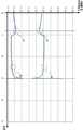
도 10은 본 발명의 일 실시예에 따른 에피택셜 반도체 기판을 제조하여 측정한 깊이에 따른 저항율과 캐리어 농도를 나타낸 도면이다.FIG. 10 is a view illustrating a resistivity and a carrier concentration according to a depth measured by manufacturing an epitaxial semiconductor substrate according to an exemplary embodiment of the present disclosure.
도 11은 본 발명의 일 실시예에 따른 에피택셜 반도체 기판을 제조하여 측정 한 소수 캐리어의 라이프 타임(minor carrier life time)을 나타낸 도면이다.FIG. 11 illustrates a minor carrier life time measured by manufacturing an epitaxial semiconductor substrate according to an exemplary embodiment of the present invention.
(도면의 주요부분에 대한 부호의 설명)(Explanation of symbols for the main parts of the drawing)
1, 2, 3: 에피택셜 반도체 기판10 : 반도체 기판1, 2, 3: epitaxial semiconductor substrate 10: semiconductor substrate
20 : 씨드층 30 : 게더링층20: seed layer 30: gathering layer
40 : 제2 에피층40: second epi layer
본 발명은 에피택셜 반도체 기판의 제조 방법 및 에피택셜 반도체 기판에 관한 것으로, 보다 상세하게는 게더링 능력이 향상된 에피택셜 반도체 기판의 제조 방법 및 이미지 센서에 관한 것이다.The present invention relates to a method for manufacturing an epitaxial semiconductor substrate and an epitaxial semiconductor substrate, and more particularly, to a method for manufacturing an epitaxial semiconductor substrate with improved gathering capability and an image sensor.
본 발명은 이미지 센서의 제조 방법 및 이미지 센서에 관한 것으로, 보다 상세하게는 동작 특성이 향상된 이미지 센서의 제조 방법 및 이미지 센서에 관한 것이다.The present invention relates to a manufacturing method and an image sensor of the image sensor, and more particularly to a manufacturing method and an image sensor of the image sensor with improved operating characteristics.
일반적으로 반도체 기판으로는 CZ(Czochralski) 방법에 의해 형성된 CZ 기판, MCZ(Magnetic field Czochralski) 방법에 의해 형성된 MCZ 기판, CZ 기판 또는 MCZ 기판 표면에 에피택셜(epitaxial)층이 형성된 에피택셜 반도체 기판 등이 사용된다. 특히, 에피택셜 반도체 기판은 도펀트 농도 불균일성(dopant concentration inhomogeneities)에 따른 이미지 컨트라스트 불균일성(image contrast unevenness)을 줄이기 위해 이미지 센서(image sensor)에 주로 사용된다.In general, semiconductor substrates include a CZ substrate formed by a CZ (Czochralski) method, an MCZ substrate formed by a magnetic field Czochralski (MCZ) method, an epitaxial semiconductor substrate having an epitaxial layer formed on a CZ substrate, or an MCZ substrate surface. This is used. In particular, epitaxial semiconductor substrates are mainly used in image sensors to reduce image contrast unevenness due to dopant concentration inhomogeneities.
에피택셜 반도체 기판은 DCS(DiChloroSilane), TCS(TriChloroSilane)등의 실리콘 소스 가스 등을 이용하여 반도체 기판 상에 결정 구조를 성장시키는데, 이 과정에서 많은 양의 불순물이 에피택셜 층에 섞이게 된다. 특히, 메탈 불순물은 SUS(steel use stainless)로 만들어진 에피택셜 성장 장치의 성장로, 소스 가스 파이프 라인에 기인한다. 즉, 염소(chloride)가 소스 가스에 포함되어 있는 경우, 에피택셜 성장하는 동안 염산(HCl)이 발생하게 된다. 염산은 SUS로 만들어진 부재를 부식시키고, 메탈 클로라이드(metal Chlorides)가 소스 가스와 에피층에 포함되게 된다. 또한, 에피택셜 반도체 기판은 디바이스 제조 과정에서 철, 구리, 니켈과 같은 중금속에 오염될 수 있다.The epitaxial semiconductor substrate grows a crystal structure on the semiconductor substrate using a silicon source gas such as DiChloroSilane (DCS) or TriChloroSilane (TCS). In this process, a large amount of impurities are mixed into the epitaxial layer. In particular, metal impurities are due to the growth of epitaxial growth devices made of SUS (steel use stainless), due to the source gas pipeline. That is, when chloride is included in the source gas, hydrochloric acid (HCl) is generated during epitaxial growth. Hydrochloric acid corrodes the members made of SUS, and metal chlorides (metal chlorides) are included in the source gas and epi layer. In addition, epitaxial semiconductor substrates may be contaminated with heavy metals such as iron, copper and nickel during device fabrication.
이러한 메탈 불순물은 에피택셜 반도체 기판을 이용하여 이미지 센서를 제조할 때, 이미지 센서에 암전류(dark-current), 백점 결함(white defects) 등을 나타나게 하는 주된 원인이 된다. 따라서, 이미지 센서의 특성 및 수율(yield)를 떨어뜨리게 된다.Such metal impurities are a major cause of dark-current, white defects, etc. appearing in the image sensor when the image sensor is manufactured using an epitaxial semiconductor substrate. Thus, the characteristics and yield of the image sensor are degraded.
종래에는 반도체 기판에 탄소를 임플란트(implant)하여 메탈 불순물을 게더링할 수 있는 게더링층을 형성하는 방법을 사용하였다. 그런데, 이와 같은 방식은 임플란트 임팩트(impact)에 의해 웨이퍼 표면이 불균일하게 되어, 백점 결함 특성을 열화시킨다. 또한, 이러한 불균일성을 보정하기 위한 어닐링(annealing) 공정이 더 필요하다.Conventionally, a method of forming a gathering layer capable of gathering metal impurities by implanting carbon into a semiconductor substrate has been used. However, such a method causes the wafer surface to be uneven due to implant impact, thereby degrading the white point defect characteristic. In addition, there is a further need for an annealing process to correct for this non-uniformity.
본 발명이 이루고자 하는 기술적 과제는, 게더링 능력이 향상된 에피택셜 반 도체 기판의 제조 방법을 제공하는 데 있다.An object of the present invention is to provide a method for manufacturing an epitaxial semiconductor substrate having improved gathering capability.
본 발명이 이루고자 하는 다른 기술적 과제는, 상기 에피택셜 반도체 기판의 제조 방법을 포함하는 이미지 센서의 제조 방법을 제공하는 데 있다.Another object of the present invention is to provide a method of manufacturing an image sensor including the method of manufacturing the epitaxial semiconductor substrate.
본 발명이 이루고자 하는 또 다른 기술적 과제는, 게더링 능력이 향상된 에피택셜 반도체 기판을 제공하는 데 있다.Another object of the present invention is to provide an epitaxial semiconductor substrate having improved gathering capability.
본 발명이 이루고자 하는 또 다른 기술적 과제는, 상기 에피택셜 반도체 기판을 포함하는 이미지 센서의 제조 방법을 제공하는 데 있다.Another object of the present invention is to provide a method of manufacturing an image sensor including the epitaxial semiconductor substrate.
본 발명의 기술적 과제들은 이상에서 언급한 기술적 과제로 제한되지 않으며, 언급되지 않은 또 다른 기술적 과제들은 아래의 기재로부터 당업자에게 명확하게 이해될 수 있을 것이다.Technical problems of the present invention are not limited to the technical problems mentioned above, and other technical problems not mentioned will be clearly understood by those skilled in the art from the following description.
상기 기술적 과제를 달성하기 위한 본 발명의 일 실시예에 따른 에피택셜 반도체 기판의 제조 방법은 실리콘 기판 상에 이온이 인-시츄 도핑된 제1 에피층을 포함하는 게더링층을 성장시키는 단계와 게더링층 상에 제2 에피층을 성장시키는 단계를 포함한다.According to one or more exemplary embodiments, a method of manufacturing an epitaxial semiconductor substrate includes growing a gathering layer including a first epi layer doped with ions in-situ on a silicon substrate, and a gathering layer. Growing a second epitaxial layer on the substrate.
상기 기술적 과제를 달성하기 위한 본 발명의 다른 실시예에 따른 이미지 센서의 제조 방법은 상기 제조 방법에 의해 제조된 에피택셜 반도체 기판을 제공하는 단계와 에피택셜 반도체 기판 상에 이미지 센서를 형성하는 단계를 포함한다.According to another aspect of the present invention, there is provided a method of manufacturing an image sensor, including providing an epitaxial semiconductor substrate manufactured by the manufacturing method, and forming an image sensor on the epitaxial semiconductor substrate. Include.
상기 기술적 과제를 달성하기 위한 본 발명의 또 다른 실시예에 따른 에피택셜 반도체 기판은 실리콘 기판, 실리콘 기판 상에 형성된 이온이 인-시츄 도핑된 제1 에피층을 포함하는 게더링층, 게더링층 상에 형성된 제2 에피층을 포함하는 에피택셜 반도체 기판을 포함한다.An epitaxial semiconductor substrate according to another embodiment of the present invention for achieving the above technical problem is on a gathering layer, a gathering layer comprising a silicon substrate, a first epi layer doped with ions formed on the silicon substrate in-situ And an epitaxial semiconductor substrate including the formed second epitaxial layer.
상기 기술적 과제를 달성하기 위한 본 발명의 또 다른 실시예에 따른 이미지 센서는 상기 에피택셜 반도체 기판 상에 형성된다.An image sensor according to another embodiment of the present invention for achieving the above technical problem is formed on the epitaxial semiconductor substrate.
본 발명의 기타 구체적인 사항들은 상세한 설명 및 도면들에 포함되어 있다.Other specific details of the invention are included in the detailed description and drawings.
본 발명의 이점 및 특징, 그리고 그것들을 달성하는 방법은 첨부되는 도면과 함께 상세하게 후술되어 있는 실시예들을 참고하면 명확해질 것이다. 그러나 본 발명은 이하에서 개시되는 실시예들에 한정되는 것이 아니라 서로 다른 다양한 형태로 구현될 것이며, 단지 본 실시예들은 본 발명의 개시가 완전하도록 하며, 본 발명이 속하는 기술분야에서 통상의 지식을 가진 자에게 발명의 범주를 완전하게 알려주기 위해 제공되는 것이며, 본 발명은 청구항의 범주에 의해 정의될 뿐이다. 명세서 전체에 걸쳐 동일 참고 부호는 동일 구성 요소를 지칭한다.Advantages and features of the present invention, and methods of achieving the same will become apparent with reference to the embodiments described below in detail in conjunction with the accompanying drawings. However, the present invention is not limited to the embodiments disclosed below, but will be implemented in various forms, and only the present embodiments are intended to complete the disclosure of the present invention, and the general knowledge in the art to which the present invention pertains. It is provided to fully convey the scope of the invention to those skilled in the art, and the present invention is defined only by the scope of the claims. Like reference numerals refer to like elements throughout.
도 1 내지 도 5을 참조하여, 본 발명의 일 실시예에 따른 에피택셜 반도체 기판의 제조 방법을 설명한다.1 to 5, a method of manufacturing an epitaxial semiconductor substrate according to an embodiment of the present invention will be described.
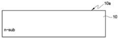
도 1 및 도 2을 참조하면, 우선 제1 및 제2 에피층을 성장시킬 반도체 기판(10)을 제공한다(S11). 이하에서, 반도체 기판(10)은 실리콘 기판을 지칭한다. 예를 들어, CZ 방법에 의해 단결정 실리콘 잉곳(ingot)을 성장시킨 후, 잉곳을 웨이퍼 형상으로 절단한다. 여기서, 반도체 기판(10)의 주면(main surface; 10a)은 경면화한다(mirror-finished). 반도체 기판(10)은 n 타입 전도성(n-type conductivity)을 가지도록 예를 들어, 인(P)이 도핑된다. 반도체 기판(10)의 크기는 지름이 8인치 이상일 수 있다.Referring to FIGS. 1 and 2, first, a
이어서, SC1(Standard Clean-1) 세정 용액(NH4OH/H2O2) 또는 BHF 용액으로 세정하여, 반도체 기판(10) 상에 존재하는 파티클(particle), 유기 불순물 등을 제거한다. 또한, 이와 같은 세정 과정은 반도체 기판의 표면의 거칠기(roughness)를 감소시키는 역할도 한다. 또한, SC2(Standard Clean-2) 세정 용액(HCl/H2O2)으로 세정하여, 천이성 금속(trace metal) 불순물을 제거할 수 있다. 그 후, 약 1100℃, 20 Torr의 수소(H2) 분위기에서 베이킹(baking)하여 반도체 기판(10) 내에 존재하는 산소를 제거한다.Subsequently, the particles are washed with a Standard Clean-1 (SC1) cleaning solution (NH4 OH / H2 O2 ) or a BHF solution to remove particles, organic impurities, and the like present on the
도 1 및 도 3을 참조하면, 반도체 기판(10) 상에 씨드층(20)을 형성한다(S21). 씨드층(20)은 500 내지 800℃의 공정 온도, 10 내지 40 Torr의 공정 압력에서 실리콘 소스 가스(silicon source gas)와 도펀트 소스 가스(dopant source gas)를 에피택셜 성장로(epitaxial reactor) 내에 공급하여, 10 내지 100nm 두께로 형성한다. 제1 에피층이 용이하게 성장될 수 있으면, 씨드층(20)의 공정 온도, 공정 압력, 공급 가스 등은 이에 제한되지 않는다.1 and 3, the
즉, 에피택셜 성장이 용이하게 형성될 수 있으면, 씨드층(20)은 1050 내지 1100℃의 공정 온도, 30 내지 60Torr의 공정 압력에서 실리콘 소스 가스만 공급하여 형성하여도 무방하다. That is, if epitaxial growth can be easily formed, the
실리콘 소스 가스로는 DCS(DiChloroSilane), TCS(TriChloroSilane), HCS(HexaChloroSilane), SiH4, Si2H6 또는 이들의 조합을 사용할 수 있고, 도펀트 소스 가스로는 PH3 또는 B2H6 등을 사용할 수 있다. 예를 들어, 실리콘 소스 가스로 SiH4, 도펀트 소스 가스로 PH3를 사용할 경우에는 각각 100sccm, 10sccm으로 공급한다.The silicon source gas may be DCS (DiChloroSilane), TCS (TriChloroSilane), HCS (HexaChloroSilane), SiH4 , Si2 H6 or a combination thereof, and as a dopant source gas, PH3 or B2 H6 may be used. have. For example, when using SiH4 as the silicon source gas and PH3 as the dopant source gas, 100 sccm and 10 sccm are respectively supplied.
또한, 씨드층(20)의 저항율(resistivity)은 20 내지 150 Ω·cm이다.In addition, the resistivity of the
도 1 및 도 4을 참조하면, 씨드층(20) 상에 이온이 인-시츄(in-situ) 도핑된 제1 에피층을 포함하는 게더링층(30)을 형성한다(S31). 여기서, 이온은 IV족 원소, 예를 들어 탄소(C), 게르마늄(Ge), 주석(Sn), 납(Pb) 또는 이들의 조합이 가능하나, 이에 제한되는 것은 아니다. 이하에서는 탄소 이온을 위주로 설명한다.1 and 4, a
게더링층(30)은 씨드층(20)이 형성되면, 실리콘 소스 가스, 탄소 소스 가스를 동시에 공급하여 형성한다. 여기서, 탄소 소스 가스는 SiH3CH3, CH4, C2H4 또는 이들의 조합을 사용할 수 있다. 또한, 게더링층(30)은 도펀트 소스 가스를 더 공급하여 성장시킬 수 있다. 예를 들어, 실리콘 소스 가스로 SiH4, 도펀트 소스 가스로 PH3, 탄소 소스 가스로 SiH3CH3를 사용할 경우에는 각각 100sccm, 10sccm, 20sccm으로 공급한다.The
또한, 게더링층(30)을 성장시키는 단계의 공정 온도는 500 내지 750℃로, 제2 에피층(도 1의 40 참조)을 성장시키는 단계의 공정 온도보다 낮은 것이 바람직하다. 여기서, 공정 온도가 500℃ 이하인 경우에는 수율이 떨어지고, 750℃ 이상인 경우에는 탄소가 실리콘 격자 사이로(interstitial) 들어가기 때문에 메탈 불순물 을 게더링 능력이 떨어지게 된다. 일반적으로 탄소 원자가 실리콘 원자와 치환되는(substitutial) 경우가 실리콘 격자 사이로 들어가는 경우보다 메탈 불순물의 게더링 능력이 더 높다고 알려져 있다. 또한, 공정 압력은 10 내지 40Torr이다.In addition, the process temperature of the step of growing the
게더링층(30)은 일반적으로 게더링층은 두꺼울수록 게더링 효율이 높기 때문에 50 nm 이상의 두께로 형성하고, 바람직하게는 100 nm 내지 1 ㎛ 정도의 두께로 형성한다. 특히, 게더링층(30)의 피크 도핑 농도(peak doping concentration)가 높을수록 메탈 불순물을 게더링하는 능력은 향상되나, 이에 따른 결점(defects)이 증가하므로, 피크 도핑 농도는 1018 내지 1021원자/cc 범위 내에서 조절하는 것이 바람직하다.In general, the
도 1 및 도 5를 참조하면, 게더링층(30) 상에 제2 에피층(40)을 성장시킨다(S41). 실리콘 소스 가스, 도펀트 소스 가스를 동시에 공급하여 형성한다. 예를 들어, 실리콘 소스 가스로 DCS, 도펀트 소스 가스로 PH3를 사용할 경우에는 각각 300sccm, 10sccm으로 공급한다.1 and 5, the
공정 온도는 1000 내지 1100℃, 공정 압력은 10 내지 760 Torr에서 5 내지 10㎛의 두께로 형성하는 것이 바람직하다. 여기서, 제2 에피층(40)을 성장시키는 단계의 공정 온도가 게더링층(30)을 성장시키는 단계의 공정 온도보다 높은 이유는 제2 에피층(40)의 성장 수율을 높이고, 실리콘 소스 가스로 쓰이는 DCS가 SiH4보다 분해 온도가 높기 때문이다.Process temperature is 1000 to 1100 ℃, process pressure is preferably formed to a thickness of 5 to 10㎛ at 10 to 760 Torr. Here, the reason why the process temperature of growing the
제2 에피층(40)은 저항율이 20 내지 150 Ω·cm인 것이 바람직하다.It is preferable that the
도 5에 도시되어 있는 바와 같이, 본 발명의 일 실시예에 따라 제조된 에피택셜 반도체 기판(1)은 반도체 기판(10), 씨드층(20), 씨드층(20) 상에 탄소가 인-시츄 도핑된 제1 에피층을 포함하는 게더링층(30), 게더링층(30) 상에 형성된 제2 에피층(40)을 포함한다.As shown in FIG. 5, the
반도체 기판(10)은 본 발명의 일 실시예에서는 n형 반도체 기판이 되도록, 예를 들어 인(P)이 도핑하였으나, 이에 제한되는 것은 아니다. 여기서, 반도체 기판(10)은 저항율이 약 10 Ω·cm일 수 있다.The
씨드층(20)은 게더링층(30)을 용이하게 성장시키기 위해 형성하며, 10 내지 100nm의 두께를 가진다. 씨드층의 저항율은 20 내지 150 Ω·cm이다. 씨드층(20)은 실리콘층, n형 실리콘층 등으로 형성될 수도 있으나 이에 제한되지 않는다. 다만, 에피택셜 반도체 기판(1)이 완성되었을 때, 씨드층(20)은 게더링층(30)의 탄소가 확산되어 분명하게 구분되지 않을 수 있다.The
게더링층(30)은 이온이 인-시츄 도핑된 제1 에피층을 포함하여, 메탈 불순물을 게더링한다. 여기서 이온은 IV족 원소, 예를 들어 탄소(C), 게르마늄(Ge), 주석(Sn), 납(Pb) 또는 이들의 조합이 가능하나, 이에 제한되는 것은 아니다. 게더링층(30)은 일반적으로 두꺼울수록 게더링 능력이 향상되므로 50nm 이상의 두께로 형성하고, 바람직하게는 100nm 내지 1 ㎛의 두께로 형성된다.The
또한, 게더링층(30)의 피크 도핑 농도(peak doping concentration)는 제2 에피층(40)보다 반도체 기판(10)에 가까이 형성되는 것이 바람직하다. 또한, 피크 도핑 농도가 높을수록 메탈 불순물을 게더링하는 능력은 향상되나, 이에 따른 결점 (defects)이 증가하므로, 게더링층(30)의 탄소의 피크 도핑 농도(peak doping concentration)는 1018 내지 1021원자/cc 범위 내에서 조절하는 것이 바람직하다.In addition, the peak doping concentration of the
다만, 탄소가 도핑된 게더링층(30)이 메탈 불순물을 게더링하는 메커니즘에 대해서 명확하게 규명된 바는 없으나, 다음과 같은 메커니즘이 알려져 있다. 우선, 원자의 반지름이 실리콘에 비해 작은 탄소가 실리콘의 위치(site)를 채워, 부피가 축소되면서 발생하는 스트레인 필드 이펙트(strain field effect)에 의해 메탈 불순물이 게더링될 수 있다고 알려져 있다. 또한, 높은 탄소 도핑 농도를 가진 영역에서는 이온화된 메탈의 용해도(solubility)가 증가하여 게더링 현상이 발생된다고 알려져 있다. 본 발명의 일 실시예에서도, 탄소가 인-시츄 도핑된 게더링층(30)에서 저항율(resistivity)은 낮아지고 캐리어 농도가 증가되므로, 이온화된 메탈이 잘 용해된다. 이에 대해서는 자세히 후술한다.However, the mechanism for gathering the metal impurity by the gathered
제2 에피층(40)은 게더링층(30) 상에 형성되고, 이는 에피택셜 반도체 기판(1) 상에 디바이스를 형성할 때 포토 다이오드와 같은 광전자 변환부가 제2 에피층(40) 내부에 위치한다. 따라서, 제2 에피층(40)은 5 내지 10㎛ 두께를 갖지만, 포토 다이오드가 내부에 충분히 형성될 정도의 두께이면 무방하다.The
또한, 제2 에피층(40)은 저항율이 20 내지 150 Ω·cm인 것이 바람직하고, 이와 같은 저항율은 포토 다이오드(Photo Diode)의 감도(sensitvity)를 높이고, 디바이스간 크로스토크(crosstalk)를 줄이기 위함이다.In addition, the
도 6은 본 발명의 다른 실시예에 따른 에피택셜 반도체 기판의 단면도이다.6 is a cross-sectional view of an epitaxial semiconductor substrate according to another embodiment of the present invention.
도 6의 에피택셜 반도체 기판(2)이 도 1의 에피택셜 반도체 기판(1)과 다른 점은, 반도체 기판(10) 내에 메탈 불순물을 게더링할 수 있는 산소 석출물(12)이 형성되어 있다는 것이다. 일반적으로 CZ법에 의해 형성된 반도체 기판(10)에는 일정량 이상의 격자간 산소가 불순물로 포함된다. 산소 불순물은 열처리 공정 등을 통해서 과포화 상태가 되기 때문에, 산소 석출물(12)이 된다. 이와 같은 산소 석출물을 이용한 게더링 방법을 인터널 게더링(Internal Gettering; IG) 방법이라 한다.The
산소 석출물(12)을 형성하는 방법은 매우 다양하다. 즉, 에피택셜 성장 후 에피택셜 반도체 기판(1)을 소정 온도, 예를 들어 450 내지 750 ℃의 온도로 적어도 30분 정도 열처리할 수 있다. 또한, 에피택셜 반도체 기판(1)을 800 ℃에서 1000 ℃까지 3℃/분의 속도로 승온하고, 1000 ℃에서 4시간 정도 열처리할 수도 있다. 또한, 석출율을 높이기 위해, 에피택셜 반도체 기판(1)에 H2, He, B, C, O2, Ge, Sb 또는 이들의 조합을 임플란트한 후, 열처리 공정을 할 수도 있다.There are many ways to form the oxygen precipitates 12. That is, after epitaxial growth, the
도 7은 본 발명의 또 다른 실시예에 따른 에피택셜 반도체 기판의 단면도이다.7 is a cross-sectional view of an epitaxial semiconductor substrate according to still another embodiment of the present invention.
도 7의 에피택셜 반도체 기판(3)이 도 1의 에피택셜 반도체 기판(1)과 다른 점은, 반도체 기판(10)의 이면에 익스트린직(extrinsic) 게더링층(14)이 형성되어 있다는 것이다. 여기서, 익스트린직 게더링층(14)은 철, 구리 등의 게더링에 효과적인 폴리 실리콘층일 수도 있고, 샌드 블라스트(sand blast) 등의 가공을 통해 형 성된 기계적인 왜곡층일 수도 있다. 이와 같은 익스트린직 게더링층(14)을 이용한 게더링 방법을 익스트린직 게더링(Extrinsic Gettering; EG) 방법이라 한다.The
예를 들어, 폴리 실리콘층을 형성하는 방법은 씨드층(20)을 성장시키기 전에, CVD 공정을 통해서 반도체 기판(10) 전체에 폴리 실리콘층을 형성한 후 주면(도 1의 10a)에 형성된 폴리 실리콘층을 연마하여 제거한다. 또한, 반도체 기판(10)의 이면에만 SiH4를 흘려, 이면에만 폴리 실리콘층을 형성할 수도 있다. 여기서, 씨드층(20) 형성하는 공정이 생략된 경우에는 제1 에피층(30)을 성장시키기 전에 폴리 실리콘 층을 형성하는 것이 바람직하다.For example, in the method of forming the polysilicon layer, before the
도 8은 본 발명의 일 실시예에 따른 이미지 센서의 제조 방법을 나타낸 순서도이다. 도 9는 본 발명의 일 실시예에 따른 이미지 센서의 단면도이다.8 is a flowchart illustrating a manufacturing method of an image sensor according to an exemplary embodiment. 9 is a cross-sectional view of an image sensor according to an embodiment of the present invention.
도 8을 참조하면, 우선 본 발명의 일 실시예에 따른 에피택셜 반도체 기판을 제공한다(S100). 즉, 제공된 반도체 기판 상에 씨드층을 성장시키고(S11, S21), 탄소가 인-시츄 도핑된 제1 에피층을 포함하는 게더링층을 성장시킨다(S31). 그 후, 게더링층 상에 제2 에피층을 성장시켜 에피택셜 반도체 기판을 완성시킨다(S41).Referring to FIG. 8, first, an epitaxial semiconductor substrate according to an embodiment of the present invention is provided (S100). That is, the seed layer is grown on the provided semiconductor substrate (S11, S21), and the gathering layer including the first epi layer doped with in-situ carbon is grown (S31). Thereafter, a second epitaxial layer is grown on the gathering layer to complete the epitaxial semiconductor substrate (S41).
완성된 에피택셜 반도체 기판 상에 이미지 센서를 형성한다(S200). 여기서, 이미지 센서는 다양한 구조를 가질 수 있으며, 예를 들어 3개 내지 5개의 트랜지스터 구조로 이루어질 수 있다. 또한, 이미지 센서의 제조 방법도 구조 및 설계에 따라 다양하게 변형될 수 있다.An image sensor is formed on the completed epitaxial semiconductor substrate (S200). Here, the image sensor may have a variety of structures, for example, may be made of three to five transistor structures. In addition, the manufacturing method of the image sensor may be variously modified according to the structure and design.
이하에서는, 본 발명의 일 실시예로서 광전자 변환부로써 핀트 포토 다이오 드(Pinned Photo Diode; PPD)를 사용하고, 4개의 트랜지스터 구조를 가진 이미지 센서를 도 9와 함께 설명한다.Hereinafter, as an embodiment of the present invention, a pinned photo diode (PPD) is used as the optoelectronic converter, and an image sensor having four transistor structures will be described with reference to FIG. 9.
도 9을 참조하면, 본 발명의 일 실시예에 따른 이미지 센서(4)는 에피택셜 반도체 기판(1), 소자 분리 영역(46), 광전자 변환부(60), 전하 검출부(70), 전하 전송부(80)를 포함한다. 에피택셜 반도체 기판(1)는 활성 영역와 소자 분리 영역이 형성되며, 본 발명의 일 실시예에서는 n형 기판 상에 별도의 p웰(42)을 형성하여 광전자 변환부(60), 전하 전송부(80) 등을 형성한다. 본 발명의 일 실시예에 따른 에피택셜 반도체 기판(1)은 메탈 불순물을 게더링할 수 있는 탄소가 인-시츄 도핑된 게더링층(30)을 포함한다.Referring to FIG. 9, an
소자 분리 영역(46)은 에피택셜 반도체 기판(1) 상의 활성 영역을 정의하고, 일반적으로 LOCOS(LOCal Oxidation of Silicon)방법을 이용한 FOX(Field OXide) 또는 STI(Shallow Trench Isolation)가 될 수 있다.The
광전자 변환부(60)는 빛 에너지를 흡수하여 발생한 전하를 축적하며, N+형의 포토 다이오드(62)와 P+형의 피닝층(pinning layer; 64)을 포함한다. 일반적으로, 포토 다이오드(62)와 피닝층(64)은 2번의 서로 다른 이온 주입 공정을 통해서 형성된다. 즉, 우선 주변의 소스, 드레인보다 더 깊게 N+ 도펀트를 이온 주입하여 포토 다이오드(62)를 형성하고, 포토 다이오드(62) 상부에 P+ 도펀트를 낮은 에너지, 높은 도즈(dose)를 이용하여 이온 주입하여 피닝층(64)을 형성한다. 물론, 도핑되는 농도 및 위치는 제조 공정 및 설계에 따라서 달라질 수 있으므로 이에 제한되지 않는다.The
전하 검출부(70)는 광전자 변환부(60)에서 축적된 전하를 전하 전송부(80)를 통해서 전송받으며, 주로 N+ 도펀트를 이온 주입하여 형성한다.The
전하 전송부(80)는 과도한 빛 에너지가 조사되었을 때 발생할 수 있는 광전자 변환부(60)에서의 오버 플로우(overflow) 및 블루밍(blooming) 현상을 막기 위해 낮은 문턱 전압(Vth)을 갖는 증가형(enhancement type) 트랜지스터 또는 공핍형(depletion type) 트랜지스터를 사용할 수 있다.The
에피택셜 반도체 기판(1) 및/또는 이미지 센서(4)를 제조하는 과정에서, 발생하는 메탈 불순물은 밸런스 밴드(valence band)와 컨덕션 밴드(conduction band) 사이에 중간갭 레벨(midgap level 또는 trap level)을 형성하게 된다. 따라서, R-G 중심을 통한 생성(R-G center generation)등의 방식을 통해서 낮은 열 에너지에 의해서도 전하가 쉽게 발생하게 된다. 따라서, 물체가 노출되어 있지 않더라도 전하 전송부(80)에서는 전하가 발생할 수 있고, 발생된 전하는 전하 전송부(80)가 비활성시에도 존재하는 채널을 통해서 이동하게 되므로 암전류가 발생된다. 또한, 불균일하게 발생한 과도한 암전류는 정상보다 큰 신호를 출력하는 ‘백점 결함(white defect)’의 원인이 된다. 뿐만 아니라, 밝음과 어두움을 명확하게 구분하지 못하므로, 이미지 센서(4)의 동적 범위(dynamic range)가 작아지게 된다. 본 발명의 일 실시예에 따른 이미지 세서(4)는 게더링층(30)을 이용하여 이러한 메탈 불순물을 게더링하므로, 암전류, 백점 결함 등의 결함을 줄일 수 있다.In the process of manufacturing the
본 발명의 또 다른 실시예에서는 이미지 센서를 예로 들었으나, 그 외의 디바이스에도 적용할 수 있음은 당업자에게 자명하다. 본 발명의 에피택셜 반도체 기판에 형성된 디바이스는 메탈 불순물의 오염이 적으므로, 디바이스의 오동작이 적고 고수명화를 도모할 수 있다.In another embodiment of the present invention, the image sensor is taken as an example, but it is apparent to those skilled in the art that the present invention can be applied to other devices. Since the device formed on the epitaxial semiconductor substrate of the present invention is less contaminated by metal impurities, the malfunction of the device is small and the service life can be extended.
본 발명에 관한 보다 상세한 내용은 다음의 구체적인 실험예들을 통하여 설명하며, 여기에 기재되지 않은 내용은 이 기술 분야에서 숙련된 자이면 충분히 기술적으로 유추할 수 있는 것이므로 설명을 생략한다.More detailed information about the present invention will be described through the following specific experimental examples, and details not described herein will be omitted because it can be inferred technically by those skilled in the art.
<실험예 1>Experimental Example 1
우선 700℃, 30 Torr의 공정 분위기에서 SiH4, PH3를 공급하여, 50nm 두께의 씨드층을 형성하였다. 그 후, 700℃, 20 Torr의 공정 분위기에서 SiH4, 100sccm, hydrogen diluted CH3SiH3 20sccm, hydrogen diluted PH3 10sccm를 공급하여 100nm 두께의 게더링층을 형성하였다. 이 때, 게더링층(30)의 탄소의 피크 도핑 농도는 5*1019원자/cc로 측정되었다. 1080℃의 공정 온도에서 DCS 100sccm, hydrogen diluted PH3 1sccm를 공급하여 6㎛ 두께의 제2 에피층을 형성하여, 테스트용 에피택셜 반도체 기판을 완성하였다.First, SiH4 and PH3 were supplied in a process atmosphere of 700 ° C. and 30 Torr to form a seed layer having a thickness of 50 nm. Thereafter, SiH4 , 100 sccm, hydrogen diluted CH3 SiH3 20 sccm, and hydrogen diluted
이어서, 테스트용 에피택셜 반도체 기판의 깊이에 따른 저항율과 캐리어 농도를 측정하였다. 그 결과가 도 10에 도시되어 있다.Next, the resistivity and the carrier concentration according to the depth of the test epitaxial semiconductor substrate were measured. The result is shown in FIG.
도 10의 x축은 깊이를 나타내고, y축은 저항율 및 캐리어 농도를 나타낸다. 여기서, 깊이, 저항율, 캐리어 농도는 표준화된 값을 사용한다. 본 실험예의 게더링층에서는 저항율(a1)은 감소하고, 캐리어 농도(b1)는 1.643*1014/cc로 증가하였음을 알 수 있다. 반면에, 제2 에피층에서는 저항율(a2)은 증가하고, 캐리어 농도(b2)는 3*1013/cc로 감소하였음을 알 수 있다. 즉, 게더링층은 캐리어의 농도가 높은 도너(donor) 타입이 되어, 이온화된 메탈의 용해도가 높아지므로 메탈 게더링 능력이 높아짐을 알 수 있다.In FIG. 10, the x axis represents depth, and the y axis represents resistivity and carrier concentration. Here, the depth, resistivity, and carrier concentration use standardized values. In the gathering layer of the present experimental example, the resistivity a1 decreased and the carrier concentration b1 increased to 1.643 * 1014 / cc. On the other hand, it can be seen that the resistivity a2 is increased in the second epitaxial layer and the carrier concentration b2 is reduced to 3 * 1013 / cc. That is, it can be seen that the gathering layer becomes a donor type having a high concentration of carrier, and the solubility of the ionized metal is increased, thereby increasing the metal gathering capability.
<실험예 2>Experimental Example 2
실험예 1에서와 동일한 방식에 따라 테스트용 에피택셜 반도체 기판을 제조한 후, 테스트용 에피택셜 반도체 기판의 소수 캐리어 라이프 타임을 측정한 결과가 도 11에 도시되어 있다.After the test epitaxial semiconductor substrate was manufactured in the same manner as in Experimental Example 1, the minority carrier life time of the test epitaxial semiconductor substrate was measured.
도 11의 y축은 표면 근처에서의 재결합 라이프 타임(near surface recombination life time)을 나타낸다. 소수 캐리어의 재결합 라이프 타임이 클수록 금속 오염량이 작음을 나타낸다. c는 에피택셜 성장 하기 전의 반도체 기판, d는 6㎛ 두께의 에피층을 성장시킨 후의 에피택셜 반도체 기판, e는 탄소의 피크 도핑 농도는 5*1019원자/cc인 게더링층을 형성하고, 6㎛ 두께의 에피층을 성장시킨 에피택셜 반도체 기판을 나타낸다. 여기서, 게더링층을 형성하면 재결합 라이프 타임이 1100msec 정도로, 게더링층이 없는 에피택셜 반도체 기판보다 게더링 성능이 개선되었음을 알 수 있다.The y axis in FIG. 11 represents the near surface recombination life time near the surface. The greater the recombination life of the minority carriers, the smaller the amount of metal contamination. c is a semiconductor substrate before epitaxial growth, d is an epitaxial semiconductor substrate after growing an epitaxial layer having a thickness of 6 μm, e is a gathering layer having a peak doping concentration of 5 * 1019 atoms / cc, and 6 An epitaxial semiconductor substrate on which an epitaxial layer having a thickness is grown is shown. Here, when the gathering layer is formed, the recombination life time is about 1100 msec, and the gathering performance is improved compared to the epitaxial semiconductor substrate without the gathering layer.
이상 첨부된 도면을 참고하여 본 발명의 실시예를 설명하였지만, 본 발명이 속하는 기술분야에서 통상의 지식을 가진 자는 본 발명이 그 기술적 사상이나 필수적인 특징을 변경하지 않고서 다른 구체적인 형태로 실시될 수 있다는 것을 이해할 수 있을 것이다. 그러므로 이상에서 기술한 실시예들은 모든 면에서 예시적인 것이며 한정적이 아닌 것으로 이해해야만 한다.Although embodiments of the present invention have been described above with reference to the accompanying drawings, those skilled in the art to which the present invention pertains may implement the present invention in other specific forms without changing the technical spirit or essential features thereof. I can understand that. Therefore, it should be understood that the embodiments described above are exemplary in all respects and not restrictive.
상기한 바와 같은 에피택셜 반도체 기판의 제조 방법 및 에피택셜 반도체 기판에 따르면 다음과 같은 효과가 하나 혹은 그 이상 있다.According to the method for manufacturing an epitaxial semiconductor substrate and the epitaxial semiconductor substrate as described above, one or more of the following effects are obtained.
첫째, 탄소가 인-시츄 도핑된 게더링층을 형성함으로써 메탈 불순물의 게더링 능력을 향상시킬 수 있다.First, by gathering a carbon-in-situ doped gathering layer, it is possible to improve the gathering ability of the metal impurities.
둘째, 인-시츄로 형성하므로 임플란트, 어닐링 등 별도의 공정이 부가되지 않는다.Second, since it is formed in-situ, a separate process such as an implant and annealing is not added.
셋째, 에피택셜 반도체 기판을 구비한 디바이스의 오동작을 방지하고, 고수명화를 도모할 수 있다.Third, malfunction of a device provided with an epitaxial semiconductor substrate can be prevented and the service life can be increased.
Claims (27)
Translated fromKoreanPriority Applications (6)
| Application Number | Priority Date | Filing Date | Title |
|---|---|---|---|
| KR1020050011459AKR100632463B1 (en) | 2005-02-07 | 2005-02-07 | Epitaxial semiconductor substrate manufacturing method and image sensor manufacturing method, epitaxial semiconductor substrate and image sensor using same |
| US11/192,085US7776723B2 (en) | 2005-02-07 | 2005-07-29 | Method of manufacturing an epitaxial semiconductor substrate and method of manufacturing a semiconductor device |
| JP2005339372AJP2006216934A (en) | 2005-02-07 | 2005-11-24 | Epitaxial semiconductor substrate manufacturing method and semiconductor device manufacturing method |
| DE102006005875.5ADE102006005875B4 (en) | 2005-02-07 | 2006-02-06 | Semiconductor substrate with getter effect, manufacturing process and use |
| CN2006100067280ACN1828836B (en) | 2005-02-07 | 2006-02-07 | Epitaxial semiconductor substrate manufacturing method and semiconductor component production method |
| TW095104007ATWI316268B (en) | 2005-02-07 | 2006-02-07 | Method of manufacturing an epitaxial semiconductor substrate and method of manufacturing a semiconductor device |
Applications Claiming Priority (1)
| Application Number | Priority Date | Filing Date | Title |
|---|---|---|---|
| KR1020050011459AKR100632463B1 (en) | 2005-02-07 | 2005-02-07 | Epitaxial semiconductor substrate manufacturing method and image sensor manufacturing method, epitaxial semiconductor substrate and image sensor using same |
Publications (2)
| Publication Number | Publication Date |
|---|---|
| KR20060090516A KR20060090516A (en) | 2006-08-11 |
| KR100632463B1true KR100632463B1 (en) | 2006-10-11 |
Family
ID=36779071
Family Applications (1)
| Application Number | Title | Priority Date | Filing Date |
|---|---|---|---|
| KR1020050011459AExpired - Fee RelatedKR100632463B1 (en) | 2005-02-07 | 2005-02-07 | Epitaxial semiconductor substrate manufacturing method and image sensor manufacturing method, epitaxial semiconductor substrate and image sensor using same |
Country Status (4)
| Country | Link |
|---|---|
| US (1) | US7776723B2 (en) |
| KR (1) | KR100632463B1 (en) |
| CN (1) | CN1828836B (en) |
| TW (1) | TWI316268B (en) |
Cited By (2)
| Publication number | Priority date | Publication date | Assignee | Title |
|---|---|---|---|---|
| US8293613B2 (en) | 2007-03-12 | 2012-10-23 | Samsung Electronics Co., Ltd. | Gettering structures and methods and their application |
| KR101224568B1 (en) | 2012-01-13 | 2013-01-21 | 주식회사 엘지실트론 | Method for manufacturing of epitaxial wafer |
Families Citing this family (29)
| Publication number | Priority date | Publication date | Assignee | Title |
|---|---|---|---|---|
| WO2008053042A1 (en)* | 2006-11-02 | 2008-05-08 | Interuniversitair Microelektronica Centrum | Removal of impurities from semiconductor device layers |
| US8008166B2 (en)* | 2007-07-26 | 2011-08-30 | Applied Materials, Inc. | Method and apparatus for cleaning a substrate surface |
| JP5311791B2 (en)* | 2007-10-12 | 2013-10-09 | 東京エレクトロン株式会社 | Method for forming polysilicon film |
| JP5499455B2 (en)* | 2007-10-22 | 2014-05-21 | 株式会社デンソー | SOI (Siliconon Insulator) Structure Semiconductor Device and Method of Manufacturing the Same |
| DE102008062040B4 (en) | 2007-12-13 | 2015-06-03 | Sumco Corporation | Epitaxial wafers and process for its production |
| US20090189159A1 (en)* | 2008-01-28 | 2009-07-30 | Atmel Corporation | Gettering layer on substrate |
| TWI442478B (en)* | 2008-03-05 | 2014-06-21 | Sumco Corp | Tantalum substrate and method of manufacturing same |
| JP2009283533A (en)* | 2008-05-20 | 2009-12-03 | Sumco Corp | Wafer for back-illuminated solid-state image sensor, method of manufacturing the same, and back-illuminated solid-state image sensor |
| US20090242939A1 (en)* | 2008-03-25 | 2009-10-01 | Sumco Corporation | Wafer for backside illumination type solid imaging device, production method thereof and backside illumination solid imaging device |
| FR2933684B1 (en)* | 2008-07-09 | 2011-05-06 | Commissariat Energie Atomique | PROCESS FOR PURIFYING CRYSTALLINE SILICON SUBSTRATE AND METHOD FOR PRODUCING PHOTOVOLTAIC CELL |
| JP5347520B2 (en)* | 2009-01-20 | 2013-11-20 | ソニー株式会社 | Method for manufacturing solid-state imaging device |
| KR101544511B1 (en)* | 2009-04-21 | 2015-08-13 | 삼성전자주식회사 | Method of manufacturing an image sensor having gettering regions |
| WO2012102755A1 (en)* | 2011-01-28 | 2012-08-02 | Applied Materials, Inc. | Carbon addition for low resistivity in situ doped silicon epitaxy |
| KR101323001B1 (en)* | 2012-02-29 | 2013-10-29 | 주식회사 엘지실트론 | Image sensor and method of manufacturing the same |
| CN103035488A (en)* | 2012-11-07 | 2013-04-10 | 上海华虹Nec电子有限公司 | Formation method of groove-shaped semiconductor structure |
| TWI541864B (en)* | 2012-12-06 | 2016-07-11 | 世創電子材料公司 | Epitaxial wafer and its manufacturing method |
| US10204803B2 (en)* | 2013-09-17 | 2019-02-12 | Deca Technologies Inc. | Two step method of rapid curing a semiconductor polymer layer |
| JP6056772B2 (en)* | 2014-01-07 | 2017-01-11 | 株式会社Sumco | Epitaxial wafer manufacturing method and epitaxial wafer |
| KR20150134543A (en)* | 2014-05-22 | 2015-12-02 | 삼성전자주식회사 | Wafer for fabricating of device and semiconductor device on the wafer |
| JP2016009730A (en)* | 2014-06-23 | 2016-01-18 | 株式会社東芝 | Manufacturing method of semiconductor device |
| EP3113224B1 (en)* | 2015-06-12 | 2020-07-08 | Canon Kabushiki Kaisha | Imaging apparatus, method of manufacturing the same, and camera |
| CN105679783B (en)* | 2016-02-24 | 2019-05-03 | 上海华虹宏力半导体制造有限公司 | Image sensor and method of forming the same |
| CN106298457A (en)* | 2016-09-22 | 2017-01-04 | 东莞市联洲知识产权运营管理有限公司 | A kind of SiGe/Si epitaxial wafer growth method |
| CN106504978A (en)* | 2016-10-17 | 2017-03-15 | 上海华力微电子有限公司 | A CIS silicon wafer processing method for improving substrate metal capture ability |
| CN107973269A (en)* | 2017-12-18 | 2018-05-01 | 中国电子科技集团公司第四十六研究所 | A kind of production method of MEMS device sandwich construction silicon chip |
| CN109192743A (en)* | 2018-09-04 | 2019-01-11 | 德淮半导体有限公司 | Imaging sensor and forming method thereof |
| CN109346489A (en)* | 2018-09-20 | 2019-02-15 | 德淮半导体有限公司 | Image sensor and method of manufacturing the same |
| WO2022104074A1 (en)* | 2020-11-13 | 2022-05-19 | The Regents Of The University Of California | Epitaxy-enabled substrate transfer |
| CN114156383B (en)* | 2021-12-03 | 2024-06-21 | 扬州乾照光电有限公司 | Semiconductor device and method for manufacturing the same |
Citations (3)
| Publication number | Priority date | Publication date | Assignee | Title |
|---|---|---|---|---|
| JP2001210650A (en) | 2000-01-05 | 2001-08-03 | Hyundai Electronics Ind Co Ltd | Method for manufacturing epitaxial silicon wafer |
| KR100328188B1 (en) | 1993-03-30 | 2002-06-20 | 이데이 노부유끼 | Semiconductor Substrate, Solid State Imaging Device and Manufacturing Method Thereof |
| JP2004165225A (en) | 2002-11-08 | 2004-06-10 | Sony Corp | Manufacturing method of semiconductor substrate, manufacturing method of solid state imaging device, and screening method for solid state imaging devices |
Family Cites Families (9)
| Publication number | Priority date | Publication date | Assignee | Title |
|---|---|---|---|---|
| JPH0237771A (en) | 1988-07-28 | 1990-02-07 | Fujitsu Ltd | Soi substrate |
| US6228453B1 (en)* | 1995-06-07 | 2001-05-08 | Lanxide Technology Company, Lp | Composite materials comprising two jonal functions and methods for making the same |
| US6548382B1 (en)* | 1997-07-18 | 2003-04-15 | Silicon Genesis Corporation | Gettering technique for wafers made using a controlled cleaving process |
| JPH11204771A (en) | 1998-01-07 | 1999-07-30 | Sony Corp | Method of manufacturing semiconductor substrate and method of manufacturing solid-state imaging device |
| JPH11297976A (en) | 1998-04-07 | 1999-10-29 | Sony Corp | Epitaxial semiconductor substrate, method for manufacturing the same, method for manufacturing semiconductor device, and method for manufacturing solid-state imaging device |
| WO2002052643A2 (en)* | 2000-12-27 | 2002-07-04 | Memc Electronic Materials, Inc. | Semiconductor wafer manufacturing process |
| US6858480B2 (en)* | 2001-01-18 | 2005-02-22 | Semiconductor Energy Laboratory Co., Ltd. | Method of manufacturing semiconductor device |
| JP2002353434A (en) | 2001-05-22 | 2002-12-06 | Sony Corp | Method for manufacturing solid-state imaging device |
| US7816236B2 (en)* | 2005-02-04 | 2010-10-19 | Asm America Inc. | Selective deposition of silicon-containing films |
- 2005
- 2005-02-07KRKR1020050011459Apatent/KR100632463B1/ennot_activeExpired - Fee Related
- 2005-07-29USUS11/192,085patent/US7776723B2/ennot_activeExpired - Fee Related
- 2006
- 2006-02-07CNCN2006100067280Apatent/CN1828836B/ennot_activeExpired - Fee Related
- 2006-02-07TWTW095104007Apatent/TWI316268B/ennot_activeIP Right Cessation
Patent Citations (3)
| Publication number | Priority date | Publication date | Assignee | Title |
|---|---|---|---|---|
| KR100328188B1 (en) | 1993-03-30 | 2002-06-20 | 이데이 노부유끼 | Semiconductor Substrate, Solid State Imaging Device and Manufacturing Method Thereof |
| JP2001210650A (en) | 2000-01-05 | 2001-08-03 | Hyundai Electronics Ind Co Ltd | Method for manufacturing epitaxial silicon wafer |
| JP2004165225A (en) | 2002-11-08 | 2004-06-10 | Sony Corp | Manufacturing method of semiconductor substrate, manufacturing method of solid state imaging device, and screening method for solid state imaging devices |
Cited By (2)
| Publication number | Priority date | Publication date | Assignee | Title |
|---|---|---|---|---|
| US8293613B2 (en) | 2007-03-12 | 2012-10-23 | Samsung Electronics Co., Ltd. | Gettering structures and methods and their application |
| KR101224568B1 (en) | 2012-01-13 | 2013-01-21 | 주식회사 엘지실트론 | Method for manufacturing of epitaxial wafer |
Also Published As
| Publication number | Publication date |
|---|---|
| TWI316268B (en) | 2009-10-21 |
| KR20060090516A (en) | 2006-08-11 |
| US20060175613A1 (en) | 2006-08-10 |
| US7776723B2 (en) | 2010-08-17 |
| TW200633022A (en) | 2006-09-16 |
| CN1828836A (en) | 2006-09-06 |
| CN1828836B (en) | 2011-04-20 |
Similar Documents
| Publication | Publication Date | Title |
|---|---|---|
| KR100632463B1 (en) | Epitaxial semiconductor substrate manufacturing method and image sensor manufacturing method, epitaxial semiconductor substrate and image sensor using same | |
| JP4650584B2 (en) | Solid-state imaging device and manufacturing method thereof | |
| KR100654354B1 (en) | Low defect epitaxial semiconductor substrate having a gathering function, an image sensor using the same, and a manufacturing method thereof | |
| KR100625944B1 (en) | Photodiode of CMOS image sensor and its manufacturing method | |
| CN102203944A (en) | Improving dark currents and reducing defects in image sensors and photovoltaic junctions | |
| US6342436B1 (en) | Method of manufacturing semiconductor substrate and method of manufacturing solid-state image-pickup device | |
| WO2002095830A1 (en) | Production method for solid imaging device | |
| US20090321883A1 (en) | Silicon substrate for solid-state imaging device and method for manufacturing the same | |
| KR101208651B1 (en) | Silicon substrate and method of producing the same | |
| TWI523206B (en) | Epitaxial wafer and its manufacturing method | |
| JP2010040864A (en) | Epitaxial silicon wafer and method of manufacturing the same | |
| KR20090095493A (en) | Method of manufacturing silicon substrate | |
| JP2007273959A (en) | Photodetector and manufacturing method thereof | |
| TW201826396A (en) | Method for manufacturing epitaxial silicon wafer, epitaxial silicon wafer, and method for manufacturing solid-state imaging element | |
| US20070205488A1 (en) | Light-detecting device and manufacturing method thereof | |
| JP3579069B2 (en) | Method for manufacturing semiconductor device | |
| KR20040066173A (en) | Silicon wafer and method for production of silicon wafer | |
| WO2014057741A1 (en) | Method for producing silicon epitaxial wafer and solid-state image-pickup element using same | |
| JP2006216934A (en) | Epitaxial semiconductor substrate manufacturing method and semiconductor device manufacturing method | |
| JP2004165225A (en) | Manufacturing method of semiconductor substrate, manufacturing method of solid state imaging device, and screening method for solid state imaging devices | |
| JP2003100760A (en) | Epitaxial silicon wafer and method for manufacturing the same | |
| JP4826993B2 (en) | Method for producing p-type silicon single crystal wafer | |
| JP2002134511A (en) | Method for manufacturing semiconductor substrate and method for manufacturing solid-state image-pickup equipment | |
| JP2007335591A (en) | Semiconductor substrate, semiconductor substrate manufacturing method, solid-state imaging device, and solid-state imaging device manufacturing method | |
| CN120568876A (en) | Technological method for improving pixel performance of CMOS image sensor |
Legal Events
| Date | Code | Title | Description |
|---|---|---|---|
| A201 | Request for examination | ||
| PA0109 | Patent application | St.27 status event code:A-0-1-A10-A12-nap-PA0109 | |
| PA0201 | Request for examination | St.27 status event code:A-1-2-D10-D11-exm-PA0201 | |
| PN2301 | Change of applicant | St.27 status event code:A-3-3-R10-R13-asn-PN2301 St.27 status event code:A-3-3-R10-R11-asn-PN2301 | |
| PN2301 | Change of applicant | St.27 status event code:A-3-3-R10-R13-asn-PN2301 St.27 status event code:A-3-3-R10-R11-asn-PN2301 | |
| D13-X000 | Search requested | St.27 status event code:A-1-2-D10-D13-srh-X000 | |
| D14-X000 | Search report completed | St.27 status event code:A-1-2-D10-D14-srh-X000 | |
| E902 | Notification of reason for refusal | ||
| PE0902 | Notice of grounds for rejection | St.27 status event code:A-1-2-D10-D21-exm-PE0902 | |
| P11-X000 | Amendment of application requested | St.27 status event code:A-2-2-P10-P11-nap-X000 | |
| P13-X000 | Application amended | St.27 status event code:A-2-2-P10-P13-nap-X000 | |
| E701 | Decision to grant or registration of patent right | ||
| PE0701 | Decision of registration | St.27 status event code:A-1-2-D10-D22-exm-PE0701 | |
| PG1501 | Laying open of application | St.27 status event code:A-1-1-Q10-Q12-nap-PG1501 | |
| GRNT | Written decision to grant | ||
| PR0701 | Registration of establishment | St.27 status event code:A-2-4-F10-F11-exm-PR0701 | |
| PR1002 | Payment of registration fee | St.27 status event code:A-2-2-U10-U11-oth-PR1002 Fee payment year number:1 | |
| PG1601 | Publication of registration | St.27 status event code:A-4-4-Q10-Q13-nap-PG1601 | |
| PR1001 | Payment of annual fee | St.27 status event code:A-4-4-U10-U11-oth-PR1001 Fee payment year number:4 | |
| PR1001 | Payment of annual fee | St.27 status event code:A-4-4-U10-U11-oth-PR1001 Fee payment year number:5 | |
| PR1001 | Payment of annual fee | St.27 status event code:A-4-4-U10-U11-oth-PR1001 Fee payment year number:6 | |
| R18-X000 | Changes to party contact information recorded | St.27 status event code:A-5-5-R10-R18-oth-X000 | |
| FPAY | Annual fee payment | Payment date:20120831 Year of fee payment:7 | |
| PR1001 | Payment of annual fee | St.27 status event code:A-4-4-U10-U11-oth-PR1001 Fee payment year number:7 | |
| FPAY | Annual fee payment | Payment date:20130902 Year of fee payment:8 | |
| PR1001 | Payment of annual fee | St.27 status event code:A-4-4-U10-U11-oth-PR1001 Fee payment year number:8 | |
| LAPS | Lapse due to unpaid annual fee | ||
| PC1903 | Unpaid annual fee | St.27 status event code:A-4-4-U10-U13-oth-PC1903 Not in force date:20140929 Payment event data comment text:Termination Category : DEFAULT_OF_REGISTRATION_FEE | |
| PC1903 | Unpaid annual fee | St.27 status event code:N-4-6-H10-H13-oth-PC1903 Ip right cessation event data comment text:Termination Category : DEFAULT_OF_REGISTRATION_FEE Not in force date:20140929 | |
| P22-X000 | Classification modified | St.27 status event code:A-4-4-P10-P22-nap-X000 |