KR100632459B1 - Heat-dissipating semiconductor package and manufacturing method - Google Patents
Heat-dissipating semiconductor package and manufacturing methodDownload PDFInfo
- Publication number
- KR100632459B1 KR100632459B1KR1020040005464AKR20040005464AKR100632459B1KR 100632459 B1KR100632459 B1KR 100632459B1KR 1020040005464 AKR1020040005464 AKR 1020040005464AKR 20040005464 AKR20040005464 AKR 20040005464AKR 100632459 B1KR100632459 B1KR 100632459B1
- Authority
- KR
- South Korea
- Prior art keywords
- heat
- semiconductor package
- slug
- semiconductor chip
- heat slug
- Prior art date
- Legal status (The legal status is an assumption and is not a legal conclusion. Google has not performed a legal analysis and makes no representation as to the accuracy of the status listed.)
- Expired - Fee Related
Links
Images


Classifications
- A—HUMAN NECESSITIES
- A01—AGRICULTURE; FORESTRY; ANIMAL HUSBANDRY; HUNTING; TRAPPING; FISHING
- A01G—HORTICULTURE; CULTIVATION OF VEGETABLES, FLOWERS, RICE, FRUIT, VINES, HOPS OR SEAWEED; FORESTRY; WATERING
- A01G9/00—Cultivation in receptacles, forcing-frames or greenhouses; Edging for beds, lawn or the like
- A01G9/12—Supports for plants; Trellis for strawberries or the like
- H—ELECTRICITY
- H01—ELECTRIC ELEMENTS
- H01L—SEMICONDUCTOR DEVICES NOT COVERED BY CLASS H10
- H01L23/00—Details of semiconductor or other solid state devices
- H01L23/28—Encapsulations, e.g. encapsulating layers, coatings, e.g. for protection
- H01L23/31—Encapsulations, e.g. encapsulating layers, coatings, e.g. for protection characterised by the arrangement or shape
- H01L23/3107—Encapsulations, e.g. encapsulating layers, coatings, e.g. for protection characterised by the arrangement or shape the device being completely enclosed
- H01L23/3121—Encapsulations, e.g. encapsulating layers, coatings, e.g. for protection characterised by the arrangement or shape the device being completely enclosed a substrate forming part of the encapsulation
- H01L23/3128—Encapsulations, e.g. encapsulating layers, coatings, e.g. for protection characterised by the arrangement or shape the device being completely enclosed a substrate forming part of the encapsulation the substrate having spherical bumps for external connection
- A—HUMAN NECESSITIES
- A01—AGRICULTURE; FORESTRY; ANIMAL HUSBANDRY; HUNTING; TRAPPING; FISHING
- A01G—HORTICULTURE; CULTIVATION OF VEGETABLES, FLOWERS, RICE, FRUIT, VINES, HOPS OR SEAWEED; FORESTRY; WATERING
- A01G17/00—Cultivation of hops, vines, fruit trees, or like trees
- A01G17/04—Supports for hops, vines, or trees
- A01G17/06—Trellis-work
- A—HUMAN NECESSITIES
- A01—AGRICULTURE; FORESTRY; ANIMAL HUSBANDRY; HUNTING; TRAPPING; FISHING
- A01G—HORTICULTURE; CULTIVATION OF VEGETABLES, FLOWERS, RICE, FRUIT, VINES, HOPS OR SEAWEED; FORESTRY; WATERING
- A01G17/00—Cultivation of hops, vines, fruit trees, or like trees
- A01G17/04—Supports for hops, vines, or trees
- A01G17/10—Holders for boughs or branches
- A—HUMAN NECESSITIES
- A01—AGRICULTURE; FORESTRY; ANIMAL HUSBANDRY; HUNTING; TRAPPING; FISHING
- A01G—HORTICULTURE; CULTIVATION OF VEGETABLES, FLOWERS, RICE, FRUIT, VINES, HOPS OR SEAWEED; FORESTRY; WATERING
- A01G7/00—Botany in general
- A01G7/06—Treatment of growing trees or plants, e.g. for preventing decay of wood, for tingeing flowers or wood, for prolonging the life of plants
- H—ELECTRICITY
- H01—ELECTRIC ELEMENTS
- H01L—SEMICONDUCTOR DEVICES NOT COVERED BY CLASS H10
- H01L23/00—Details of semiconductor or other solid state devices
- H01L23/34—Arrangements for cooling, heating, ventilating or temperature compensation ; Temperature sensing arrangements
- H01L23/42—Fillings or auxiliary members in containers or encapsulations selected or arranged to facilitate heating or cooling
- H01L23/433—Auxiliary members in containers characterised by their shape, e.g. pistons
- H01L23/4334—Auxiliary members in encapsulations
- H—ELECTRICITY
- H01—ELECTRIC ELEMENTS
- H01L—SEMICONDUCTOR DEVICES NOT COVERED BY CLASS H10
- H01L2224/00—Indexing scheme for arrangements for connecting or disconnecting semiconductor or solid-state bodies and methods related thereto as covered by H01L24/00
- H01L2224/01—Means for bonding being attached to, or being formed on, the surface to be connected, e.g. chip-to-package, die-attach, "first-level" interconnects; Manufacturing methods related thereto
- H01L2224/42—Wire connectors; Manufacturing methods related thereto
- H01L2224/44—Structure, shape, material or disposition of the wire connectors prior to the connecting process
- H01L2224/45—Structure, shape, material or disposition of the wire connectors prior to the connecting process of an individual wire connector
- H01L2224/45001—Core members of the connector
- H01L2224/45099—Material
- H01L2224/451—Material with a principal constituent of the material being a metal or a metalloid, e.g. boron (B), silicon (Si), germanium (Ge), arsenic (As), antimony (Sb), tellurium (Te) and polonium (Po), and alloys thereof
- H01L2224/45117—Material with a principal constituent of the material being a metal or a metalloid, e.g. boron (B), silicon (Si), germanium (Ge), arsenic (As), antimony (Sb), tellurium (Te) and polonium (Po), and alloys thereof the principal constituent melting at a temperature of greater than or equal to 400°C and less than 950°C
- H01L2224/45124—Aluminium (Al) as principal constituent
- H—ELECTRICITY
- H01—ELECTRIC ELEMENTS
- H01L—SEMICONDUCTOR DEVICES NOT COVERED BY CLASS H10
- H01L2224/00—Indexing scheme for arrangements for connecting or disconnecting semiconductor or solid-state bodies and methods related thereto as covered by H01L24/00
- H01L2224/01—Means for bonding being attached to, or being formed on, the surface to be connected, e.g. chip-to-package, die-attach, "first-level" interconnects; Manufacturing methods related thereto
- H01L2224/42—Wire connectors; Manufacturing methods related thereto
- H01L2224/44—Structure, shape, material or disposition of the wire connectors prior to the connecting process
- H01L2224/45—Structure, shape, material or disposition of the wire connectors prior to the connecting process of an individual wire connector
- H01L2224/45001—Core members of the connector
- H01L2224/45099—Material
- H01L2224/451—Material with a principal constituent of the material being a metal or a metalloid, e.g. boron (B), silicon (Si), germanium (Ge), arsenic (As), antimony (Sb), tellurium (Te) and polonium (Po), and alloys thereof
- H01L2224/45138—Material with a principal constituent of the material being a metal or a metalloid, e.g. boron (B), silicon (Si), germanium (Ge), arsenic (As), antimony (Sb), tellurium (Te) and polonium (Po), and alloys thereof the principal constituent melting at a temperature of greater than or equal to 950°C and less than 1550°C
- H01L2224/45144—Gold (Au) as principal constituent
- H—ELECTRICITY
- H01—ELECTRIC ELEMENTS
- H01L—SEMICONDUCTOR DEVICES NOT COVERED BY CLASS H10
- H01L2224/00—Indexing scheme for arrangements for connecting or disconnecting semiconductor or solid-state bodies and methods related thereto as covered by H01L24/00
- H01L2224/01—Means for bonding being attached to, or being formed on, the surface to be connected, e.g. chip-to-package, die-attach, "first-level" interconnects; Manufacturing methods related thereto
- H01L2224/42—Wire connectors; Manufacturing methods related thereto
- H01L2224/44—Structure, shape, material or disposition of the wire connectors prior to the connecting process
- H01L2224/45—Structure, shape, material or disposition of the wire connectors prior to the connecting process of an individual wire connector
- H01L2224/45001—Core members of the connector
- H01L2224/45099—Material
- H01L2224/451—Material with a principal constituent of the material being a metal or a metalloid, e.g. boron (B), silicon (Si), germanium (Ge), arsenic (As), antimony (Sb), tellurium (Te) and polonium (Po), and alloys thereof
- H01L2224/45138—Material with a principal constituent of the material being a metal or a metalloid, e.g. boron (B), silicon (Si), germanium (Ge), arsenic (As), antimony (Sb), tellurium (Te) and polonium (Po), and alloys thereof the principal constituent melting at a temperature of greater than or equal to 950°C and less than 1550°C
- H01L2224/45147—Copper (Cu) as principal constituent
- H—ELECTRICITY
- H01—ELECTRIC ELEMENTS
- H01L—SEMICONDUCTOR DEVICES NOT COVERED BY CLASS H10
- H01L2224/00—Indexing scheme for arrangements for connecting or disconnecting semiconductor or solid-state bodies and methods related thereto as covered by H01L24/00
- H01L2224/01—Means for bonding being attached to, or being formed on, the surface to be connected, e.g. chip-to-package, die-attach, "first-level" interconnects; Manufacturing methods related thereto
- H01L2224/42—Wire connectors; Manufacturing methods related thereto
- H01L2224/47—Structure, shape, material or disposition of the wire connectors after the connecting process
- H01L2224/48—Structure, shape, material or disposition of the wire connectors after the connecting process of an individual wire connector
- H01L2224/481—Disposition
- H01L2224/48151—Connecting between a semiconductor or solid-state body and an item not being a semiconductor or solid-state body, e.g. chip-to-substrate, chip-to-passive
- H01L2224/48221—Connecting between a semiconductor or solid-state body and an item not being a semiconductor or solid-state body, e.g. chip-to-substrate, chip-to-passive the body and the item being stacked
- H01L2224/48225—Connecting between a semiconductor or solid-state body and an item not being a semiconductor or solid-state body, e.g. chip-to-substrate, chip-to-passive the body and the item being stacked the item being non-metallic, e.g. insulating substrate with or without metallisation
- H01L2224/48227—Connecting between a semiconductor or solid-state body and an item not being a semiconductor or solid-state body, e.g. chip-to-substrate, chip-to-passive the body and the item being stacked the item being non-metallic, e.g. insulating substrate with or without metallisation connecting the wire to a bond pad of the item
- H—ELECTRICITY
- H01—ELECTRIC ELEMENTS
- H01L—SEMICONDUCTOR DEVICES NOT COVERED BY CLASS H10
- H01L2224/00—Indexing scheme for arrangements for connecting or disconnecting semiconductor or solid-state bodies and methods related thereto as covered by H01L24/00
- H01L2224/73—Means for bonding being of different types provided for in two or more of groups H01L2224/10, H01L2224/18, H01L2224/26, H01L2224/34, H01L2224/42, H01L2224/50, H01L2224/63, H01L2224/71
- H01L2224/732—Location after the connecting process
- H01L2224/73251—Location after the connecting process on different surfaces
- H01L2224/73265—Layer and wire connectors
- H—ELECTRICITY
- H01—ELECTRIC ELEMENTS
- H01L—SEMICONDUCTOR DEVICES NOT COVERED BY CLASS H10
- H01L24/00—Arrangements for connecting or disconnecting semiconductor or solid-state bodies; Methods or apparatus related thereto
- H01L24/01—Means for bonding being attached to, or being formed on, the surface to be connected, e.g. chip-to-package, die-attach, "first-level" interconnects; Manufacturing methods related thereto
- H01L24/42—Wire connectors; Manufacturing methods related thereto
- H01L24/44—Structure, shape, material or disposition of the wire connectors prior to the connecting process
- H01L24/45—Structure, shape, material or disposition of the wire connectors prior to the connecting process of an individual wire connector
- H—ELECTRICITY
- H01—ELECTRIC ELEMENTS
- H01L—SEMICONDUCTOR DEVICES NOT COVERED BY CLASS H10
- H01L24/00—Arrangements for connecting or disconnecting semiconductor or solid-state bodies; Methods or apparatus related thereto
- H01L24/01—Means for bonding being attached to, or being formed on, the surface to be connected, e.g. chip-to-package, die-attach, "first-level" interconnects; Manufacturing methods related thereto
- H01L24/42—Wire connectors; Manufacturing methods related thereto
- H01L24/47—Structure, shape, material or disposition of the wire connectors after the connecting process
- H01L24/48—Structure, shape, material or disposition of the wire connectors after the connecting process of an individual wire connector
- H—ELECTRICITY
- H01—ELECTRIC ELEMENTS
- H01L—SEMICONDUCTOR DEVICES NOT COVERED BY CLASS H10
- H01L2924/00—Indexing scheme for arrangements or methods for connecting or disconnecting semiconductor or solid-state bodies as covered by H01L24/00
- H01L2924/0001—Technical content checked by a classifier
- H01L2924/00014—Technical content checked by a classifier the subject-matter covered by the group, the symbol of which is combined with the symbol of this group, being disclosed without further technical details
- H—ELECTRICITY
- H01—ELECTRIC ELEMENTS
- H01L—SEMICONDUCTOR DEVICES NOT COVERED BY CLASS H10
- H01L2924/00—Indexing scheme for arrangements or methods for connecting or disconnecting semiconductor or solid-state bodies as covered by H01L24/00
- H01L2924/01—Chemical elements
- H01L2924/01079—Gold [Au]
- H—ELECTRICITY
- H01—ELECTRIC ELEMENTS
- H01L—SEMICONDUCTOR DEVICES NOT COVERED BY CLASS H10
- H01L2924/00—Indexing scheme for arrangements or methods for connecting or disconnecting semiconductor or solid-state bodies as covered by H01L24/00
- H01L2924/10—Details of semiconductor or other solid state devices to be connected
- H01L2924/11—Device type
- H01L2924/14—Integrated circuits
- H01L2924/143—Digital devices
- H01L2924/1433—Application-specific integrated circuit [ASIC]
- H—ELECTRICITY
- H01—ELECTRIC ELEMENTS
- H01L—SEMICONDUCTOR DEVICES NOT COVERED BY CLASS H10
- H01L2924/00—Indexing scheme for arrangements or methods for connecting or disconnecting semiconductor or solid-state bodies as covered by H01L24/00
- H01L2924/15—Details of package parts other than the semiconductor or other solid state devices to be connected
- H01L2924/151—Die mounting substrate
- H01L2924/153—Connection portion
- H01L2924/1531—Connection portion the connection portion being formed only on the surface of the substrate opposite to the die mounting surface
- H01L2924/15311—Connection portion the connection portion being formed only on the surface of the substrate opposite to the die mounting surface being a ball array, e.g. BGA
- H—ELECTRICITY
- H01—ELECTRIC ELEMENTS
- H01L—SEMICONDUCTOR DEVICES NOT COVERED BY CLASS H10
- H01L2924/00—Indexing scheme for arrangements or methods for connecting or disconnecting semiconductor or solid-state bodies as covered by H01L24/00
- H01L2924/15—Details of package parts other than the semiconductor or other solid state devices to be connected
- H01L2924/161—Cap
- H01L2924/1615—Shape
- H01L2924/16152—Cap comprising a cavity for hosting the device, e.g. U-shaped cap
- H—ELECTRICITY
- H01—ELECTRIC ELEMENTS
- H01L—SEMICONDUCTOR DEVICES NOT COVERED BY CLASS H10
- H01L2924/00—Indexing scheme for arrangements or methods for connecting or disconnecting semiconductor or solid-state bodies as covered by H01L24/00
- H01L2924/15—Details of package parts other than the semiconductor or other solid state devices to be connected
- H01L2924/181—Encapsulation
Landscapes
- Life Sciences & Earth Sciences (AREA)
- Engineering & Computer Science (AREA)
- Microelectronics & Electronic Packaging (AREA)
- Physics & Mathematics (AREA)
- Environmental Sciences (AREA)
- Condensed Matter Physics & Semiconductors (AREA)
- General Physics & Mathematics (AREA)
- Computer Hardware Design (AREA)
- Power Engineering (AREA)
- Botany (AREA)
- Forests & Forestry (AREA)
- Ecology (AREA)
- Biodiversity & Conservation Biology (AREA)
- Wood Science & Technology (AREA)
- Cooling Or The Like Of Semiconductors Or Solid State Devices (AREA)
- Structures Or Materials For Encapsulating Or Coating Semiconductor Devices Or Solid State Devices (AREA)
Abstract
Translated fromKoreanDescription
Translated fromKorean도 1은 종래기술에 따른 볼 그리드 어레이(이하, BGA) 패키지를 나타내는 단면도이다.1 is a cross-sectional view showing a ball grid array (hereinafter referred to as BGA) package according to the prior art.
도 2a 내지 도 2e는 본 발명의 일 실시예에 따른 반도체 패키지의 제조 방법을 순서대로 도시한 단면도들이다.2A through 2E are cross-sectional views sequentially illustrating a method of manufacturing a semiconductor package according to an embodiment of the present invention.
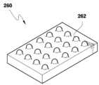
도 3a 내지 도 3c는 본 발명의 일 실시예에 의한 반도체 패키지에 적용되는 히트 슬러그를 나타낸 사시도들이다.3A to 3C are perspective views illustrating heat slugs applied to a semiconductor package according to an embodiment of the present invention.
<도면의 주요 부분에 관한 부호의 설명><Explanation of symbols on main parts of the drawings>
200: 반도체 패키지210: 기판200: semiconductor package 210: substrate
220: 접착제230: 반도체 칩220: adhesive 230: semiconductor chip
240: 본딩수단250: 접착제240: bonding means 250: adhesive
260: 히트 슬러그270: 히트 스프레더260: heat slug 270: heat spreader
272: 상판부274: 지지부272: top portion 274: support portion
280: 절연성 봉지수지290: 솔더볼280: insulating encapsulation resin 290: solder ball
본 발명은 열방출형 반도체 패키지 및 그 제조방법에 관한 것으로, 좀더 상세하게는 히트 스프레더와 히트 슬러그를 이용하여, 반도체 칩의 고속동작에 의해 발생되는 열을 외부로 신속히 방출시킴으로써, 방열장애로 인한 반도체 칩의 고장을 미리 방지할 수 있도록 하는 열방출형 반도체 패키지 및 그 제조방법에 관한 것이다.The present invention relates to a heat dissipation-type semiconductor package and a method of manufacturing the same, and more particularly, by using a heat spreader and a heat slug to quickly discharge the heat generated by the high-speed operation of the semiconductor chip to the outside, The present invention relates to a heat dissipation-type semiconductor package and a method of manufacturing the same that can prevent failure of a semiconductor chip in advance.
일반적으로 고속 또는 높은 주파수 특성을 갖는 ASICs(Application Specific Integrated circuits) 제품이나 DRAM 및 SRAM과 같은 고속 반도체 메모리 장치에 적용되어 전자소자(electrical component)를 포함하는 반도체 패키지가 가져야 할 가장 중요한 특성 중의 하나는 열방출(Thermal dissipation)에 있다.In general, one of the most important characteristics of a semiconductor package including an electrical component is to be applied to an ASIC (Application Specific Integrated Circuits) product having high speed or high frequency characteristics or a high speed semiconductor memory device such as DRAM and SRAM. It is in thermal dissipation.
최근의 반도체 장치들은 고속화 및 고출력화를 요구함에 따라 이에 대응되는 패키지 개발이 필요하게 되었으며, 현재 개발 중이거나 개발된 패키지를 크게 두 갈래로 나누어 보면 다음과 같다.Recently, as semiconductor devices require high speed and high output, there is a need to develop a package corresponding thereto, and the package currently being developed or developed is divided into two parts as follows.
즉, 반도체 패키지는 고출력화를 요구하는 전력단의 측면에서 파워 트랜지스터나 모듈장치에 히트 싱크가 주로 부착되는 플라스틱 패키지 형태로 제작되거나, 세라믹 기판에 메탈 하우징을 함으로써 소자 동작시 발생되는 열을 쉽게 방출하는 구조로 되어 있다.That is, the semiconductor package is manufactured in the form of a plastic package in which a heat sink is mainly attached to a power transistor or a module device in terms of a power stage requiring high output, or a metal housing on a ceramic substrate to easily release heat generated during device operation. It is made to structure.
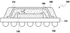
도 1은 종래기술에 따른 볼 그리드 어레이(이하, BGA) 패키지를 나타내는 단면도이다.1 is a cross-sectional view showing a ball grid array (hereinafter referred to as BGA) package according to the prior art.
도 1에 도시된 바와 같이, BGA 패키지(100)는 기판(110), 반도체 칩(130) 및 히트 싱크(Heat sink)(170)를 포함한다.As shown in FIG. 1, the BGA
여기서, 기판(110) 상면에는 반도체 칩(130)이 접합되어 있고, 이 기판(110)과 반도체 칩(130)은 와이어 본딩(140)에 의해 전기적으로 접속되어 있다. 이와 같이 구성된 BGA 패키지(100)는 반도체 칩(130) 내 형성된 전자소자가 동작할 때 발생되는 열을 BGA 패키지(100) 외부로 효과적으로 방출하기 위해 히트 싱크(170)가 설치되어 있다. 즉, 도 1에 도시된 바와 같이, 히트 싱크(170)는 반도체 칩(130)의 상부에 위치하고 일면은 BGA 패키지(100) 외부로 노출되어 있어서, 반도체 칩(140)으로부터 발생하는 열을 쉽게 외부로 방출할 수 있는 구조를 가진다.Here, the
이러한 히트 싱크(170)를 배치한 후 기판(110) 상에 배치된 반도체 칩(130), 와이어 본딩(140) 및 히트 싱크(170)를 절연성 봉지수지(180)로 봉지한다. 다만, 위에서 언급한 바와 같이 히트 싱크(170)의 일면은 BGA 패키지(100) 외부로 노출되도록 절연성 봉지수지(180)로 봉지한다.After the
그리고, 반도체 칩(130)이 실장된 기판(110) 하면에는 솔더볼(190)이 형성되어 있다.The
이와 같이 종래 기술에 의한 히트 싱크(170)를 포함하는 BGA 패키지(100)는 히트 싱크(170)가 BGA 패키지(100) 표면에 노출되도록 하여, 반도체 칩(130) 상에 형성된 전자소자의 동작시 발생되는 열을 외부로 방출하기 쉽도록 하여 히트 싱크(170)가 없는 일반적인 BGA 패키지(100)에 비해 열특성을 향상시켰다.As described above, the
여기서, 종래의 히트 싱크(170)를 포함하는 BGA 패키지(100)의 경우, 반도체 칩(130)에서 발생한 열의 일부는 반도체 칩(130) 하부에 위치한 기판(110)을 통하 여 외부로 방출되고, 나머지는 반도체 칩(130) 상부에 위치한 히트 싱크(170)를 통하여 외부로 방출된다.Here, in the case of the
이때, 반도체 칩(130)과 기판(110)을 연결시키는 와이어 본딩(140)에 손상을 주지 않도록 하기 위하여 히트 싱크(170)는 반도체 칩(130)으로부터 약 300 내지 400 ㎛ 정도로 이격되게 배치한다(도 1의 L1). 이러한 이격공간(L1)은 절연성 봉지수지(180)로 충진된다. 일반적으로 히트 싱크(170)는 열전도성이 높은 물질, 예를 들어 금속물질을 사용하지만, 절연성 봉지수지(180)는 열전도율이 낮다고 알려져 있다.In this case, in order not to damage the wire bonding 140 connecting the
따라서, 히트 싱크(170)와 반도체 칩(130)이 직접 접촉하지 않는 종래 기술에 의한 BGA 패키지(100)의 경우 반도체 칩(130)에서 발생하는 열은 대부분 복사열의 형태로 히트 싱크(170)에 전달되기 때문에 열방출이 비효율적인 문제가 발생한다.Therefore, in the case of the
본 발명이 이루고자 하는 기술적 과제는, 다양한 형태의 열방출수단을 부여함으로써 반도체 칩 상에 형성된 전자소자의 동작시 발생되는 열을 효과적으로 방출하여 전자소자 동작의 신뢰성을 향상시킬 수 있고, 이러한 열방출수단을 배치한 후 절연성 봉지수지로 봉지하는 동안 금형에 의해 반도체 칩에 압력이 가해지는 것을 방지할 수 있는 열방출형 반도체 패키지를 제공하고자 하는 것이다.The technical problem to be achieved by the present invention, by providing various types of heat dissipation means can effectively release the heat generated during the operation of the electronic device formed on the semiconductor chip to improve the reliability of the operation of the electronic device, such heat dissipation means It is to provide a heat dissipation-type semiconductor package that can prevent the pressure is applied to the semiconductor chip by the mold during the sealing after the insulating encapsulation resin is disposed.
또한, 본 발명이 이루고자 하는 다른 기술적 과제는, 다양한 형태의 열방출수단을 부여함으로써 반도체 칩 상에 형성된 전자소자의 동작시 발생되는 열을 효 과적으로 방출하여 전자소자 동작의 신뢰성을 향상시킬 수 있고, 이러한 열방출수단을 배치한 후 절연성 봉지수지로 봉지하는 동안 금형에 의해 반도체 칩에 압력이 가해지는 것을 방지할 수 있는 열방출형 반도체 패키지의 제조방법을 제공하고자 하는 것이다.In addition, another technical problem to be achieved by the present invention, by providing various types of heat dissipation means can effectively release the heat generated during the operation of the electronic device formed on the semiconductor chip to improve the reliability of the electronic device operation The present invention is to provide a method of manufacturing a heat dissipation type semiconductor package which can prevent pressure from being applied to the semiconductor chip by a mold while the heat dissipation means is disposed and encapsulated with an insulating encapsulation resin.
상기 기술적 과제를 달성하기 위한 본 발명의 일 실시예에 따른 열방출형 반도체 패키지는 기판과, 상기 기판 상에 실장되고 상기 기판과 본딩수단에 의해 전기적으로 연결되는 반도체 칩과, 상기 반도체 칩과 접합되고 열전도성 물질로 형성된 히트 슬러그와, 반도체 패키지의 외부로 일부 노출되고 상기 히트 슬러그 상부에 상기 히트 슬러그와 버퍼간격을 두고 배치되는 히트 스프레더를 포함한다.According to an aspect of the present invention, there is provided a heat-dissipating semiconductor package including a substrate, a semiconductor chip mounted on the substrate, and electrically connected by the substrate and bonding means, and bonded to the semiconductor chip. And a heat slug formed of a thermally conductive material, and a heat spreader partially exposed to the outside of the semiconductor package and disposed on the heat slug with a buffer interval therebetween.
또한, 상기 다른 다른 기술적 과제를 달성하기 위한 본 발명의 일 실시예에 따른 열방출형 반도체 패키지의 제조방법은 기판에 반도체 칩을 부착시키고 본딩수단에 의해 기판과 반도체 칩을 전기적으로 연결시키는 단계와, 상기 반도체 칩 상면에 열전도성 물질로 형성된 히트 슬러그를 접합시키는 단계와, 상기 히트 슬러그 상부에 상기 히트 슬러그와 버퍼간격을 두고 히트 스프레더를 배치시키는 단계를 포함한다.In addition, the method of manufacturing a heat dissipation semiconductor package according to an embodiment of the present invention for achieving the other technical problem and the step of attaching a semiconductor chip to the substrate and electrically connecting the substrate and the semiconductor chip by the bonding means; And bonding a heat slug formed of a thermally conductive material to an upper surface of the semiconductor chip, and disposing a heat spreader on the heat slug with a gap between the heat slug and a buffer.
기타 실시예들의 구체적인 사항들은 상세한 설명 및 도면들에 포함되어 있다.Specific details of other embodiments are included in the detailed description and the drawings.
본 발명의 이점 및 특징, 그리고 그것들을 달성하는 방법은 첨부되는 도면과 함께 상세하게 후술되어 있는 실시예들을 참조하면 명확해질 것이다. 그러나 본 발 명은 이하에서 개시되는 실시예들에 한정되는 것이 아니라 서로 다른 다양한 형태로 구현될 것이며, 단지 본 실시예들은 본 발명의 개시가 완전하도록 하며, 본 발명이 속하는 기술분야에서 통상의 지식을 가진 자에게 발명의 범주를 완전하게 알려주기 위해 제공되는 것이며, 본 발명은 청구항의 범주에 의해 정의될 뿐이다. 명세서 전체에 걸쳐 동일 참조 부호는 동일 구성 요소를 지칭한다.Advantages and features of the present invention and methods for achieving them will be apparent with reference to the embodiments described below in detail with the accompanying drawings. However, the present invention is not limited to the embodiments disclosed below, but may be implemented in various forms, and only the embodiments are to make the disclosure of the present invention complete, and the general knowledge in the technical field to which the present invention belongs. It is provided to fully convey the scope of the invention to those skilled in the art, and the invention is defined only by the scope of the claims. Like reference numerals refer to like elements throughout.
이하 본 발명의 실시예들에 따른 반도체 패키지는 고주파수 특성을 갖는 마이크로 프로세서나 ASIC 제품 또는 DRAM 및 SRAM 등과 같은 고속 메모리 장치들을 구성한다. 이러한 장치들은 대부분 다핀 입/출력단자를 가지고 있으며, 이를 구성하는 반도체 패키지들도 대부분 다핀구조를 가질 수 있도록 플라스틱 또는 세라믹 재질의 핀 그리드 어레이(Pin Grid Array) 타입 패키지, 랜드 그리드 어레이(Land Grid Array) 타입 패키지, 볼 그리드 어레이(Ball Grid Array) 타입 패키지, 쿼드 프랫트(Quad Flat) 타입 패키지 또는 리드 프래임(Lead frame) 타입 패키지 등으로 구성될 수 있다.Hereinafter, the semiconductor package according to the embodiments of the present invention constitutes a high-speed memory device such as a microprocessor or an ASIC product or a DRAM and an SRAM. Most of these devices have multi-pin I / O terminals, and the semiconductor packages constituting most of them have a multi-pin structure, such as a pin grid array type package made of plastic or ceramic material, and a land grid array. ) Package, a ball grid array type package, a quad flat type package, or a lead frame type package.
또한, 본 발명에 따른 반도체 패키지에 적용될 수 있는 기판은 핀 그리드 어레이(PGA) 타입, 랜드 그리드 어레이(LGA) 타입, 볼 그리드 어레이(BGA) 타입, 쿼드 프랫트(Quad Flat) 타입 패키지 또는 리드 프래임(Lead frame) 타입 패키지 등과 같은 반도체 패키지에 적용될 수 있도록 인쇄회로기판, 세라믹 기판, 메탈기판, 실리콘 기판 등이 될 수 있다.In addition, the substrate applicable to the semiconductor package according to the present invention may be a pin grid array (PGA) type, a land grid array (LGA) type, a ball grid array (BGA) type, a quad flat type package or a lead frame. It may be a printed circuit board, a ceramic substrate, a metal substrate, a silicon substrate, or the like to be applied to a semiconductor package such as a lead frame type package.
이하, 본 발명의 실시예들에서는 설명의 편의를 위하여 반도체 패키지로 볼 그리드 어레이(이하, BGA) 패키지를, 기판으로 인쇄회로기판을 예로 들어 설명한 다.Hereinafter, in the embodiments of the present invention, a ball grid array (hereinafter, referred to as BGA) package as a semiconductor package and a printed circuit board as a substrate will be described for convenience of description.
이하, 본 발명의 일 실시예를 도 2a 내지 도 2e에 근거하여 설명한다. 도 2a 내지 도 2e는 본 발명의 일 실시예에 따른 반도체 패키지의 제조 방법을 순서대로 도시한 단면도들이고, 도 2e는 이 제조방법에 의해 제조된 본 발명의 일 실시예에 의한 반도체 패키지의 단면도이다.Hereinafter, an embodiment of the present invention will be described with reference to FIGS. 2A to 2E. 2A to 2E are cross-sectional views sequentially illustrating a method of manufacturing a semiconductor package according to an embodiment of the present invention, and FIG. 2E is a cross-sectional view of a semiconductor package according to an embodiment of the present invention manufactured by this manufacturing method. .
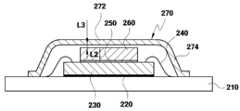
도 2e에 도시된 바와 같이, 본 발명의 일 실시예에 의한 반도체 패키지(200)는 기판(210), 반도체 칩(230), 히트 슬러그(Heat Slug)(260) 및 히트 스프레더(Heat Spreader)(270)로 구성된다.As shown in FIG. 2E, the
여기서, 기판(210)은 하부에 형성된 다수개의 솔더볼(Solder ball)(290)을 구비한다. 이 솔더볼(290)을 기판(210)에 부착하는 단계는 본 발명의 반도체 패키지(200)의 제조공정 중 순서에 상관없이 임의의 단계에서 수행될 수 있다.Here, the
그리고, 반도체 칩(230)은 기판(210) 상면에 실장되고 반도체 칩(230)과 기판(210)은 접착제(220)에 의해 접합된다. 여기서, 접착제(220)는 대표적으로 실버 페이스트(Silver paste)를 사용할 수 있다. 그리고, 반도체 칩(230)은 고주파수 특성을 갖는 마이크로 프로세서나 ASIC 제품 또는 DRAM 및 SRAM 등과 같은 고속 메모리 등이 구현된 칩이다.The
반도체 칩(230)의 본딩패드(미도시)와 기판(210)의 전극패드(미도시)는 본딩수단(240)에 의해 전기적으로 연결된다. 본 발명의 일 실시예에 있어서, 본딩수단(240)은 와이어 본딩을 예로 들어 설명하였으나, 본 발명은 이에 한정되는 것은 아니다. 즉, 반도체 칩(230)과 기판(210)의 전기적 접속은 플립칩본딩에 의해 서도 가능할 것이다. 와이어 본딩에서 사용되는 와이어는 금(Gold), 구리(Copper), 알루미늄(Aluminum) 또는 이들의 조합으로 이루어진 물질을 사용하여 형성시킨다.Bonding pads (not shown) of the
히트 슬러그(260)는 열전도성 물질로 구성되며, 반도체 칩(230)의 상부와 접합된다. 여기서, 히트 슬러그(260)는 구리(Copper), 구리 합금(Copper alloy), 알루미늄(Aluminum), 알루미늄 합금(Aluminum alloy), 스틸(Steel), 스텐레스 스틸(Stainless steel) 또는 이들의 조합으로 이루어진 고열전도성 물질로 이루어진 그룹에서 선택된 어느 하나의 물질로 이루어지는 것이 바람직하다. 또한, 히트 슬러그(260)는 세라믹, 절연체 또는 반도체 물질로 이루어진 그룹에서 선택된 어느 하나의 열전도성 물질로 이루어질 수 있다. 히트 슬러그(260)는 주물, 단조 또는 프레스성형 등의 방식으로 제조할 수 있다.The
히트 슬러그(260)는 반도체 칩(230)과 접착제(250)에 의해 접합될 수 있다.The
여기서, 접착제(250)는 반도체 칩(230)의 표면에 영향을 주지 않아야 하며 히트 슬러그(260)를 적절히 지지해 주어야 한다. 접착제(250)는 전기절연체이지만 열전도체인 것이 바람직하다. 또한, 접착제(250)는 열전도성 수지인 것이 바람직하며, 더욱 바람직하게는 접착제(250)로서 실리콘 러버(Silicon rubber) 또는 엘라스토머(Elastomer) 재질의 완충 접합제를 사용한다. 이러한 접착제(250)는 외부의 충격이 반도체칩으로 전달되는 것을 완충 차단시킴으로써, 반도체칩이 외력에 의해 손상되는 것을 미리 방지시키는 역할을 수행한다. 또한, 히트 슬러그(260)와 반도체 칩(230) 사이의 열팽창계수 차이에 따른 히트 슬러그(260)의 박리를 미리 방지할 수 있다.Here, the adhesive 250 should not affect the surface of the
또한, 이러한 접착제(250)는 열가소성 접착 수지(Thermo - plastic adhesive epoxy), 열경화성 접착 수지(Thermo - set adhesive epoxy), 열전도성 수지(Thermal conductive epoxy), 접착 테잎(Adhesive tape) 또는 이들의 조합을 사용할 수 있다.In addition, the adhesive 250 may be formed of a thermoplastic adhesive epoxy, a thermoset adhesive epoxy, a thermal conductive epoxy, an adhesive tape, or a combination thereof. Can be used.
본 발명의 일 실시예에 따른 히트 슬러그(260)는 반도체 칩(230)과 후술할 히트 스프레더(270) 사이에 배치되므로 히트 슬러그(260)의 두께(L2)는 약 200 내지 400 ㎛인 것이 바람직하다.Since the
도 3a 내지 도 3c는 본 발명의 일 실시예에 의한 히트 슬러그를 나타낸 사시도이다. 도 3a 내지 도 3c에 도시된 바와 같이, 본 발명의 일 실시예에 따른 히트 슬러그(260)는 일면이 평평한 모양(262)이 될 수 있다. 또한, 히트 슬러그(260)는 일면이 요철 모양(264)이거나 일면에 홈(266)이 형성되어 반도체 칩(230)으로부터 발생된 열의 방출효과를 극대화 할 수 있다.3A to 3C are perspective views illustrating a heat slug according to an embodiment of the present invention. As shown in FIGS. 3A to 3C, the
도 2e에 도시된 바와 같이, 히트 슬러그(260) 상부에 히트 슬러그(260)와 버퍼간격(L3)을 두고 히트 스프레더(270)를 배치한다. 히트 스프레더(270)는 히트 슬러그(260)와 버퍼역할을 할 수 있는 간격, 예컨대 약 100 ㎛ 이하의 버퍼간격(L3)을 두고 배치되는 것이 바람직하다. 여기서, 버퍼간격(L3)은 봉지시 가해지는 압력이 반도체 칩(230)에 미치지 않도록 버퍼역할을 하고, 히트 슬러그(260)로부터의 열을 히트 스프레더(270)로 전달하는 열전달역할을 한다. 이와 같이, 히트 슬러그(260)와 히트 스프레더(270) 사이에 얇은 간격(L3)을 두고 배치함으로써, 이후 절연성 봉지수지(280)에 의해 기판(210) 상의 구조물을 봉지할 때 금형의 압력 에 의해 반도체 칩(230)이 손상되는 것을 방지할 수 있다. 이러한 역할들을 수행하기 위해 버퍼간격(L3)는 약 20 내지 30 ㎛인 것이 더욱 바람직하다.As illustrated in FIG. 2E, the
그리고, 히트 스프레더(270)는 히트 슬러그(260) 상부에 히트 슬러그(260)와 소정의 간격(L3)을 두고 배치되는 상판부(272)와, 상판부(272)의 가장자리의 저면에 형성되고 기판(210)과 접합하여 상판부(272)를 지지하는 지지부(274)를 포함한다. 여기서, 히트 스프레더(270)의 상판부(272)는 약 100 내지 200 ㎛의 두께를 가지고, 평평한 모양을 가진다. 그리고, 히트 스프레더(270)는 구리, 구리 합금, 알루미늄, 알루미늄 합금, 스틸, 스텐레스 스틸, 또는 이들의 조합으로 이루어진 고열전도성 물질로 이루어진 그룹에서 선택된 어느 하나의 물질로 이루어지는 것이 바람직하다. 히트 스프레더(270)는 주물, 단조 또는 프레스성형 등의 방식으로 제조할 수 있다.The
외부로부터의 충격으로부터 기판(210) 상에 실장된 반도체 칩(230), 히트 스프레더(270) 및 히트 슬러그(260)를 보호하기 위하여 절연성 봉지수지(280)로 봉지한다. 다만, 도 2e에 도시된 바와 같이, 히트 스프레더(270)로부터 효율적으로 열이 외부로 방출되기 위하여 히트 스프레더(270)의 상판부(272)의 일면이 노출되도록 기판(210), 반도체 칩(230), 히트 슬러그(260) 및 히트 스프레더(270)의 지지부(274)를 절연성 봉지수지(280)로 봉지한다. 여기서, 절연성 봉지수지(280)로는 예를 들어 EMC(Epoxy molding compound)를 사용할 수 있다.In order to protect the
상술한 본 발명에서, 외부 시스템보드(System board)(미도시)로부터 출력된 전기적인 신호는 솔더볼(290), 기판(210), 본딩수단(240) 등을 경유하여, 반도체 칩(230)으로 입력된다. 역으로, 반도체 칩(230)으로부터 출력된 전기적인 신호는 본딩수단(240), 기판(210), 솔더볼(290)을 경유하여 외부 시스템보드(미도시)로 입력된다. 이러한 전기신호 입·출력 과정을 통해 반도체 칩(230)은 신속한 구동을 이루게 되며, 이에 비례하여, 반도체 칩(230)에서는 많은 량의 열이 방출되게 된다.In the present invention described above, the electrical signal output from the external system board (System board) (not shown) via the
이때, 본 발명에서는 상술한 바와 같이, 반도체 칩(230) 상부에 열전도성이 높은 히트 슬러그(260)와 히트 스프레더(270)를 배치하기 때문에, 반도체 칩(230)이 고속동작에 의해 많은 양의 열을 발산하더라도 이를 히트 슬러그(260)와 히트 스프레더(270)를 이용하여 좀더 원활하게 방출할 수 있게 되며, 그 결과 열방출의 미비로 인한 반도체 칩(230)의 고장을 미리 방지할 수 있다.At this time, in the present invention, since the
이하, 도 2a 내지 도 2e를 참조하여 본 발명의 일 실시예에 의한 반도체 패키지의 제조방법을 설명한다.Hereinafter, a method of manufacturing a semiconductor package according to an embodiment of the present invention will be described with reference to FIGS. 2A to 2E.
도 2a는 반도체 칩(230)의 부착 및 본딩 단계로서, 실버 페이스트와 같은 접착제(220)를 사용하여 반도체 칩(230)을 기판(210)에 부착시킨다. 그리고, 본딩수단(240)에 의해 기판(210)의 전극패드(미도시)와 반도체 칩(230)의 본딩패드(미도시)를 전기적으로 연결한다.FIG. 2A illustrates a step of attaching and bonding the
도 2b는 히트 슬러그(260) 접합단계로서, 반도체 칩(230)의 상면에 배치된 I/O 본딩패드(미도시)가 손상되지 않도록 반도체 칩(230) 상면에 접착제(250)를 도포한 후 히트 슬러그(260)를 접합시킨다.2B illustrates a step of bonding the
도 2c는 히트 스프레더(270) 접합단계로서, 히트 슬러그(260) 상부에 히트 슬러그(260)와 소정의 간격(L3)를 두고 히트 스프레더(270)를 배치시킨다.FIG. 2C illustrates a step of joining the
도 2d는 봉지 단계로서, 반도체 칩(230), 본딩수단(240), 히트 슬러그(260) 및 히트 스프레더(270)를 보호하기 위하여 에폭시 몰딩 컴파운드(Epoxy Molding Compound)와 같은 절연성 봉지수지(280)를 사용하여 몰딩한다. 여기서, 열방출 효율을 높이기 위해 히트 스프레더(270)의 상면은 절연성 봉지수지(280)에 의해 덮히지 않도록 한다.2D illustrates an encapsulation step, in which an insulating
도 2e는 외부 I/O 단자 형성 단계로서, 봉지가 완료된 반도체 패키지(200)의 외부 I/O 단자, 즉 본 도면에서는 솔더볼(290)을 형성한다. 이러한, 외부 I/O 단자 형성 단계는 봉지 단계 후에 실시하는 것이 바람직하지만, 이에 한정되지 않으며 이상에서 설명한 반도체 패키지(200) 제조공정 중 순서에 상관없이 임의의 단계에서 실시할 수 있다.2E illustrates an external I / O terminal forming step, in which the
이상 첨부된 도면을 참조하여 본 발명의 실시예를 설명하였지만, 본 발명이 속하는 기술분야에서 통상의 지식을 가진 자는 본 발명의 기술적 사상이나 필수적인 특징을 변경하지 않고서 다른 구체적인 형태로 실시될 수 있다는 것을 이해할 수 있을 것이다. 그러므로 이상에서 기술한 실시예들은 모든 면에서 예시적인 것이며 한정적이 아닌 것으로 이해해야만 한다.Although the embodiments of the present invention have been described above with reference to the accompanying drawings, those skilled in the art to which the present invention pertains may be embodied in other specific forms without changing the technical spirit or essential features of the present invention. I can understand. Therefore, it should be understood that the embodiments described above are exemplary in all respects and not restrictive.
상술한 바와 같이 본 발명에 따른 열방출형 반도체 패키지 및 그 제조방법에 의하면, 고열전도성 소재로 구성된 히트 스프레더와 히트 슬러그의 작용에 의해 신속한 반도체 칩의 열방출을 원활히 할 수 있다.As described above, according to the heat dissipation-type semiconductor package and the manufacturing method thereof, the heat dissipation of the semiconductor chip can be smoothly performed by the action of the heat spreader and the heat slug made of the high thermal conductivity material.
또한, 히트 슬러그와 반도체 칩 사이의 접착제 및 히트 슬러그와 히트 스프레더 사이의 간격에 의해, 절연성 봉지수지로 봉지시 반도체 칩을 안정적으로 보호할 수 있게 된다. 즉, 본 반도체 패키지는 반도체 칩 열방출기능과 반도체 칩 보호기능을 동시에 수행할 수 있게 됨으로써, 우수한 성능을 장시간 유지할 수 있다.In addition, by the adhesive between the heat slug and the semiconductor chip, and the gap between the heat slug and the heat spreader, it is possible to stably protect the semiconductor chip when sealed with an insulating encapsulating resin. That is, the semiconductor package can simultaneously perform the semiconductor chip heat dissipation function and the semiconductor chip protection function, thereby maintaining excellent performance for a long time.
Claims (25)
Translated fromKoreanPriority Applications (5)
| Application Number | Priority Date | Filing Date | Title |
|---|---|---|---|
| KR1020040005464AKR100632459B1 (en) | 2004-01-28 | 2004-01-28 | Heat-dissipating semiconductor package and manufacturing method |
| JP2005017033AJP2005217405A (en) | 2004-01-28 | 2005-01-25 | Heat emission type semiconductor package and manufacturing method thereof |
| CNA2005100656670ACN1697169A (en) | 2004-01-28 | 2005-01-28 | Semiconductor package with heat dissipation structure and manufacturing method thereof |
| US11/046,514US7202561B2 (en) | 2004-01-28 | 2005-01-28 | Semiconductor package with heat dissipating structure and method of manufacturing the same |
| US11/680,470US20070138625A1 (en) | 2004-01-28 | 2007-02-28 | Semiconductor package with heat dissipating structure and method of manufacturing the same |
Applications Claiming Priority (1)
| Application Number | Priority Date | Filing Date | Title |
|---|---|---|---|
| KR1020040005464AKR100632459B1 (en) | 2004-01-28 | 2004-01-28 | Heat-dissipating semiconductor package and manufacturing method |
Publications (2)
| Publication Number | Publication Date |
|---|---|
| KR20050077866A KR20050077866A (en) | 2005-08-04 |
| KR100632459B1true KR100632459B1 (en) | 2006-10-09 |
Family
ID=34909919
Family Applications (1)
| Application Number | Title | Priority Date | Filing Date |
|---|---|---|---|
| KR1020040005464AExpired - Fee RelatedKR100632459B1 (en) | 2004-01-28 | 2004-01-28 | Heat-dissipating semiconductor package and manufacturing method |
Country Status (4)
| Country | Link |
|---|---|
| US (2) | US7202561B2 (en) |
| JP (1) | JP2005217405A (en) |
| KR (1) | KR100632459B1 (en) |
| CN (1) | CN1697169A (en) |
Families Citing this family (30)
| Publication number | Priority date | Publication date | Assignee | Title |
|---|---|---|---|---|
| US20070013042A1 (en)* | 2005-06-20 | 2007-01-18 | Nokia Corporation | Electronic module assembly with heat spreader |
| DE102006007303A1 (en)* | 2006-02-16 | 2007-08-30 | Infineon Technologies Ag | Printed circuit board, has grouting cover element, in which multiple chips connected electrically with printed circuit board, are embedded |
| US9299634B2 (en) | 2006-05-16 | 2016-03-29 | Broadcom Corporation | Method and apparatus for cooling semiconductor device hot blocks and large scale integrated circuit (IC) using integrated interposer for IC packages |
| US9013035B2 (en) | 2006-06-20 | 2015-04-21 | Broadcom Corporation | Thermal improvement for hotspots on dies in integrated circuit packages |
| US20080042302A1 (en)* | 2006-08-16 | 2008-02-21 | Crispell Robert B | Plastic overmolded packages with molded lid attachments |
| JP5259945B2 (en)* | 2006-10-30 | 2013-08-07 | スリーエム イノベイティブ プロパティズ カンパニー | IC socket with heat dissipation function |
| JP4861200B2 (en)* | 2007-01-15 | 2012-01-25 | シャープ株式会社 | Power module |
| US8013440B2 (en)* | 2008-03-28 | 2011-09-06 | Conexant Systems, Inc. | Enhanced thermal dissipation ball grid array package |
| CN101635284B (en)* | 2008-07-24 | 2011-08-03 | 环旭电子股份有限公司 | Wafer packaging structure |
| WO2010038345A1 (en)* | 2008-10-03 | 2010-04-08 | パナソニック株式会社 | Wiring board, semiconductor device and method for manufacturing the same |
| US20110012257A1 (en)* | 2009-07-14 | 2011-01-20 | Freescale Semiconductor, Inc | Heat spreader for semiconductor package |
| US8120056B2 (en)* | 2009-10-19 | 2012-02-21 | Avago Technologies Ecbu Ip (Singapore) Pte. Ltd. | Light emitting diode assembly |
| KR101129073B1 (en)* | 2009-12-29 | 2012-03-23 | 하나 마이크론(주) | Heat Radiating Type Semiconductor Package |
| KR101115714B1 (en) | 2009-12-30 | 2012-03-06 | 하나 마이크론(주) | Method For Fabricating a Heat Radiating Type Semiconductor Package |
| US7999371B1 (en)* | 2010-02-09 | 2011-08-16 | Amkor Technology, Inc. | Heat spreader package and method |
| JP2012033559A (en) | 2010-07-28 | 2012-02-16 | J Devices:Kk | Semiconductor device |
| TWI431697B (en) | 2010-11-08 | 2014-03-21 | Advanced Semiconductor Eng | Manufacturing method for semiconductor package and packaging mold for manufacturing the same |
| US8552540B2 (en) | 2011-05-10 | 2013-10-08 | Conexant Systems, Inc. | Wafer level package with thermal pad for higher power dissipation |
| FR2977975A1 (en)* | 2011-07-13 | 2013-01-18 | St Microelectronics Grenoble 2 | THERMAL VIA ELECTRONIC HOUSING AND METHOD OF MANUFACTURE |
| KR101992596B1 (en)* | 2011-08-16 | 2019-06-25 | 삼성전자 주식회사 | Memory device |
| CN202839587U (en) | 2012-07-27 | 2013-03-27 | 飞思卡尔半导体公司 | Surface mounting semiconductor device |
| KR101463936B1 (en)* | 2013-08-19 | 2014-11-26 | 주식회사 휘닉스소재 | Graphene coating with excellent adhesion to the heat sink for semiconductor package and a method of manufacturing |
| US20150136357A1 (en)* | 2013-11-21 | 2015-05-21 | Honeywell Federal Manufacturing & Technologies, Llc | Heat dissipation assembly |
| KR20150142915A (en) | 2014-06-12 | 2015-12-23 | 에스티에스반도체통신 주식회사 | Semiconductor package and method for manufacturing the same |
| KR101640126B1 (en) | 2014-06-12 | 2016-07-15 | 주식회사 에스에프에이반도체 | Semiconductor package manufacturing method |
| KR20150142916A (en) | 2014-06-12 | 2015-12-23 | 에스티에스반도체통신 주식회사 | Semiconductor package and method for manufacturing the same |
| KR101613114B1 (en) | 2014-06-12 | 2016-04-19 | 주식회사 에스에프에이반도체 | Semiconductor package and method for manufacturing the same |
| CN109148397B (en)* | 2017-06-16 | 2023-02-28 | 日月光半导体制造股份有限公司 | Semiconductor device package |
| KR102601150B1 (en)* | 2019-08-23 | 2023-11-09 | 삼성전자주식회사 | Semiconductor package |
| TWI761864B (en)* | 2020-06-19 | 2022-04-21 | 海華科技股份有限公司 | Chip scale package structure with heat-dissipating type |
Citations (6)
| Publication number | Priority date | Publication date | Assignee | Title |
|---|---|---|---|---|
| JPH04155853A (en)* | 1990-10-19 | 1992-05-28 | Hitachi Ltd | Semiconductor integrated circuit device |
| JPH07142647A (en)* | 1993-11-15 | 1995-06-02 | Nec Corp | Semiconductor device |
| KR950024313A (en)* | 1994-01-11 | 1995-08-21 | 김광호 | High heat dissipation semiconductor package |
| JP2000077575A (en)* | 1998-08-28 | 2000-03-14 | Ind Technol Res Inst | Thermally and electrically enhanced semiconductor package |
| KR20000045081A (en)* | 1998-12-30 | 2000-07-15 | 마이클 디. 오브라이언 | Semiconductor package structure |
| KR20030082178A (en)* | 2002-04-17 | 2003-10-22 | 주식회사 칩팩코리아 | Tebga package |
Family Cites Families (16)
| Publication number | Priority date | Publication date | Assignee | Title |
|---|---|---|---|---|
| US5610442A (en)* | 1995-03-27 | 1997-03-11 | Lsi Logic Corporation | Semiconductor device package fabrication method and apparatus |
| KR19990067623A (en)* | 1995-11-28 | 1999-08-25 | 가나이 쓰도무 | Semiconductor device, manufacturing method and mounting board |
| US5883782A (en)* | 1997-03-05 | 1999-03-16 | Intel Corporation | Apparatus for attaching a heat sink to a PCB mounted semiconductor package |
| US5894166A (en)* | 1997-09-17 | 1999-04-13 | Northern Telecom Limited | Chip mounting scheme |
| TW411595B (en)* | 1999-03-20 | 2000-11-11 | Siliconware Precision Industries Co Ltd | Heat structure for semiconductor package device |
| US6559525B2 (en)* | 2000-01-13 | 2003-05-06 | Siliconware Precision Industries Co., Ltd. | Semiconductor package having heat sink at the outer surface |
| JP3768079B2 (en)* | 2000-07-25 | 2006-04-19 | シャープ株式会社 | Transistor |
| TW454321B (en)* | 2000-09-13 | 2001-09-11 | Siliconware Precision Industries Co Ltd | Semiconductor package with heat dissipation structure |
| US6400014B1 (en)* | 2001-01-13 | 2002-06-04 | Siliconware Precision Industries Co., Ltd. | Semiconductor package with a heat sink |
| JP2002270717A (en)* | 2001-03-12 | 2002-09-20 | Rohm Co Ltd | Semiconductor device |
| JP4103342B2 (en)* | 2001-05-22 | 2008-06-18 | 日立電線株式会社 | Manufacturing method of semiconductor device |
| US6734552B2 (en)* | 2001-07-11 | 2004-05-11 | Asat Limited | Enhanced thermal dissipation integrated circuit package |
| KR100447867B1 (en)* | 2001-10-05 | 2004-09-08 | 삼성전자주식회사 | Semiconductor package |
| US6882041B1 (en)* | 2002-02-05 | 2005-04-19 | Altera Corporation | Thermally enhanced metal capped BGA package |
| US20030178719A1 (en)* | 2002-03-22 | 2003-09-25 | Combs Edward G. | Enhanced thermal dissipation integrated circuit package and method of manufacturing enhanced thermal dissipation integrated circuit package |
| TW535244B (en)* | 2002-04-19 | 2003-06-01 | Advanced Semiconductor Eng | Wafer level package method and package structure |
- 2004
- 2004-01-28KRKR1020040005464Apatent/KR100632459B1/ennot_activeExpired - Fee Related
- 2005
- 2005-01-25JPJP2005017033Apatent/JP2005217405A/ennot_activeWithdrawn
- 2005-01-28CNCNA2005100656670Apatent/CN1697169A/enactivePending
- 2005-01-28USUS11/046,514patent/US7202561B2/ennot_activeExpired - Lifetime
- 2007
- 2007-02-28USUS11/680,470patent/US20070138625A1/ennot_activeAbandoned
Patent Citations (6)
| Publication number | Priority date | Publication date | Assignee | Title |
|---|---|---|---|---|
| JPH04155853A (en)* | 1990-10-19 | 1992-05-28 | Hitachi Ltd | Semiconductor integrated circuit device |
| JPH07142647A (en)* | 1993-11-15 | 1995-06-02 | Nec Corp | Semiconductor device |
| KR950024313A (en)* | 1994-01-11 | 1995-08-21 | 김광호 | High heat dissipation semiconductor package |
| JP2000077575A (en)* | 1998-08-28 | 2000-03-14 | Ind Technol Res Inst | Thermally and electrically enhanced semiconductor package |
| KR20000045081A (en)* | 1998-12-30 | 2000-07-15 | 마이클 디. 오브라이언 | Semiconductor package structure |
| KR20030082178A (en)* | 2002-04-17 | 2003-10-22 | 주식회사 칩팩코리아 | Tebga package |
Also Published As
| Publication number | Publication date |
|---|---|
| CN1697169A (en) | 2005-11-16 |
| US20050224957A1 (en) | 2005-10-13 |
| JP2005217405A (en) | 2005-08-11 |
| US20070138625A1 (en) | 2007-06-21 |
| US7202561B2 (en) | 2007-04-10 |
| KR20050077866A (en) | 2005-08-04 |
Similar Documents
| Publication | Publication Date | Title |
|---|---|---|
| KR100632459B1 (en) | Heat-dissipating semiconductor package and manufacturing method | |
| US10204848B2 (en) | Semiconductor chip package having heat dissipating structure | |
| KR970005712B1 (en) | High heat sink package | |
| KR100312236B1 (en) | Integral design features for heatsink attach for electronic packages | |
| US5705851A (en) | Thermal ball lead integrated package | |
| US6429513B1 (en) | Active heat sink for cooling a semiconductor chip | |
| US6404049B1 (en) | Semiconductor device, manufacturing method thereof and mounting board | |
| US6143590A (en) | Multi-chip semiconductor device and method of producing the same | |
| US6330158B1 (en) | Semiconductor package having heat sinks and method of fabrication | |
| US7892882B2 (en) | Methods and apparatus for a semiconductor device package with improved thermal performance | |
| US6566164B1 (en) | Exposed copper strap in a semiconductor package | |
| JP4493121B2 (en) | Semiconductor device and semiconductor chip packaging method | |
| US20080093733A1 (en) | Chip package and manufacturing method thereof | |
| US20200312734A1 (en) | Semiconductor package with an internal heat sink and method for manufacturing the same | |
| US6501164B1 (en) | Multi-chip semiconductor package with heat dissipating structure | |
| CN103915405B (en) | Semiconductor device and method of making a semiconductor device | |
| US6700783B1 (en) | Three-dimensional stacked heat spreader assembly for electronic package and method for assembling | |
| CN1437233A (en) | Packaged semiconductor device and method of forming the same | |
| US6437984B1 (en) | Thermally enhanced chip scale package | |
| KR100220249B1 (en) | Thermally enhanced thin ball grid array package | |
| JP3894749B2 (en) | Semiconductor device | |
| JP4349728B2 (en) | Semiconductor device | |
| JP3058142B2 (en) | Semiconductor device and manufacturing method thereof | |
| KR0163864B1 (en) | Heat dissipation structure of stacked semiconductor package | |
| JPH0878616A (en) | Multi-chip module |
Legal Events
| Date | Code | Title | Description |
|---|---|---|---|
| A201 | Request for examination | ||
| PA0109 | Patent application | St.27 status event code:A-0-1-A10-A12-nap-PA0109 | |
| PA0201 | Request for examination | St.27 status event code:A-1-2-D10-D11-exm-PA0201 | |
| PN2301 | Change of applicant | St.27 status event code:A-3-3-R10-R13-asn-PN2301 St.27 status event code:A-3-3-R10-R11-asn-PN2301 | |
| PN2301 | Change of applicant | St.27 status event code:A-3-3-R10-R13-asn-PN2301 St.27 status event code:A-3-3-R10-R11-asn-PN2301 | |
| PG1501 | Laying open of application | St.27 status event code:A-1-1-Q10-Q12-nap-PG1501 | |
| D13-X000 | Search requested | St.27 status event code:A-1-2-D10-D13-srh-X000 | |
| D14-X000 | Search report completed | St.27 status event code:A-1-2-D10-D14-srh-X000 | |
| E902 | Notification of reason for refusal | ||
| PE0902 | Notice of grounds for rejection | St.27 status event code:A-1-2-D10-D21-exm-PE0902 | |
| E13-X000 | Pre-grant limitation requested | St.27 status event code:A-2-3-E10-E13-lim-X000 | |
| P11-X000 | Amendment of application requested | St.27 status event code:A-2-2-P10-P11-nap-X000 | |
| P13-X000 | Application amended | St.27 status event code:A-2-2-P10-P13-nap-X000 | |
| E701 | Decision to grant or registration of patent right | ||
| PE0701 | Decision of registration | St.27 status event code:A-1-2-D10-D22-exm-PE0701 | |
| GRNT | Written decision to grant | ||
| PR0701 | Registration of establishment | St.27 status event code:A-2-4-F10-F11-exm-PR0701 | |
| PR1002 | Payment of registration fee | St.27 status event code:A-2-2-U10-U11-oth-PR1002 Fee payment year number:1 | |
| PG1601 | Publication of registration | St.27 status event code:A-4-4-Q10-Q13-nap-PG1601 | |
| PR1001 | Payment of annual fee | St.27 status event code:A-4-4-U10-U11-oth-PR1001 Fee payment year number:4 | |
| PR1001 | Payment of annual fee | St.27 status event code:A-4-4-U10-U11-oth-PR1001 Fee payment year number:5 | |
| PR1001 | Payment of annual fee | St.27 status event code:A-4-4-U10-U11-oth-PR1001 Fee payment year number:6 | |
| R18-X000 | Changes to party contact information recorded | St.27 status event code:A-5-5-R10-R18-oth-X000 | |
| FPAY | Annual fee payment | Payment date:20120831 Year of fee payment:7 | |
| PR1001 | Payment of annual fee | St.27 status event code:A-4-4-U10-U11-oth-PR1001 Fee payment year number:7 | |
| FPAY | Annual fee payment | Payment date:20130902 Year of fee payment:8 | |
| PR1001 | Payment of annual fee | St.27 status event code:A-4-4-U10-U11-oth-PR1001 Fee payment year number:8 | |
| FPAY | Annual fee payment | Payment date:20140901 Year of fee payment:9 | |
| PR1001 | Payment of annual fee | St.27 status event code:A-4-4-U10-U11-oth-PR1001 Fee payment year number:9 | |
| FPAY | Annual fee payment | Payment date:20150831 Year of fee payment:10 | |
| PR1001 | Payment of annual fee | St.27 status event code:A-4-4-U10-U11-oth-PR1001 Fee payment year number:10 | |
| PR1001 | Payment of annual fee | St.27 status event code:A-4-4-U10-U11-oth-PR1001 Fee payment year number:11 | |
| PR1001 | Payment of annual fee | St.27 status event code:A-4-4-U10-U11-oth-PR1001 Fee payment year number:12 | |
| FPAY | Annual fee payment | Payment date:20180831 Year of fee payment:13 | |
| PR1001 | Payment of annual fee | St.27 status event code:A-4-4-U10-U11-oth-PR1001 Fee payment year number:13 | |
| PR1001 | Payment of annual fee | St.27 status event code:A-4-4-U10-U11-oth-PR1001 Fee payment year number:14 | |
| PR1001 | Payment of annual fee | St.27 status event code:A-4-4-U10-U11-oth-PR1001 Fee payment year number:15 | |
| PR1001 | Payment of annual fee | St.27 status event code:A-4-4-U10-U11-oth-PR1001 Fee payment year number:16 | |
| PR1001 | Payment of annual fee | St.27 status event code:A-4-4-U10-U11-oth-PR1001 Fee payment year number:17 | |
| PC1903 | Unpaid annual fee | St.27 status event code:A-4-4-U10-U13-oth-PC1903 Not in force date:20230929 Payment event data comment text:Termination Category : DEFAULT_OF_REGISTRATION_FEE | |
| PC1903 | Unpaid annual fee | St.27 status event code:N-4-6-H10-H13-oth-PC1903 Ip right cessation event data comment text:Termination Category : DEFAULT_OF_REGISTRATION_FEE Not in force date:20230929 |