KR100631851B1 - Non-volatile memory cell having 2 bits and manufacturing method thereof - Google Patents
Non-volatile memory cell having 2 bits and manufacturing method thereofDownload PDFInfo
- Publication number
- KR100631851B1 KR100631851B1KR1020050028377AKR20050028377AKR100631851B1KR 100631851 B1KR100631851 B1KR 100631851B1KR 1020050028377 AKR1020050028377 AKR 1020050028377AKR 20050028377 AKR20050028377 AKR 20050028377AKR 100631851 B1KR100631851 B1KR 100631851B1
- Authority
- KR
- South Korea
- Prior art keywords
- dielectric
- substrate
- bits
- gates
- control
- Prior art date
- Legal status (The legal status is an assumption and is not a legal conclusion. Google has not performed a legal analysis and makes no representation as to the accuracy of the status listed.)
- Expired - Fee Related
Links
Images


Classifications
- H—ELECTRICITY
- H10—SEMICONDUCTOR DEVICES; ELECTRIC SOLID-STATE DEVICES NOT OTHERWISE PROVIDED FOR
- H10B—ELECTRONIC MEMORY DEVICES
- H10B41/00—Electrically erasable-and-programmable ROM [EEPROM] devices comprising floating gates
- H10B41/20—Electrically erasable-and-programmable ROM [EEPROM] devices comprising floating gates characterised by three-dimensional arrangements, e.g. with cells on different height levels
Landscapes
- Non-Volatile Memory (AREA)
- Semiconductor Memories (AREA)
Abstract
Translated fromKoreanDescription
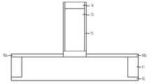
Translated fromKorean도 1은 본 발명의 바람직한 실시예에 따른 2비트를 갖는 비휘발성 메모리 셀의 단면도.1 is a cross-sectional view of a non-volatile memory cell with two bits in accordance with a preferred embodiment of the present invention.
도 2 내지 도 8은 본 발명의 바람직한 실시예에 따른 2비트를 갖는 비휘발성 메모리 셀의 제조방법을 설명하기 위하여 도시한 공정단면도.2 to 8 are cross-sectional views illustrating a method of manufacturing a nonvolatile memory cell having two bits in accordance with a preferred embodiment of the present invention.
〈도면의 주요 부분에 대한 부호의 설명〉<Explanation of symbols for main parts of drawing>
10 : 반도체 기판11 : 소자분리막10
12 : 제1 게이트 절연막13 : 제1 컨트롤 게이트12 first gate
14 : 층간 절연막15 : 제1 유전체막14 interlayer
16a, 16b : 제1 터널 산화막, 제2 터널 산화막16a, 16b: first tunnel oxide film and second tunnel oxide film
17a, 17b : 제1 플로팅 게이트, 제2 플로팅 게이트17a, 17b: first floating gate, second floating gate
18a, 18b : 제2 유전체막, 제3 유전체막19a : 제2 게이트 절연막18a, 18b: second dielectric film, third
19b : 제3 게이트 절연막21 : 스페이서19b: third gate insulating film 21: spacer
20a, 20b : 제2 컨트롤 게이트, 제3 컨트롤 게이트20a, 20b: second control gate, third control gate
22a, 22b : 제1 접합영역, 제2 접합영역23 : 실리사이드층22a, 22b: first junction region, second junction region 23: silicide layer
본 발명은 2비트를 갖는 비휘발성 메모리 셀 및 그 제조방법에 관한 것으로, 특히, 2비트를 갖는 플래시(FLASH) 메모리 소자의 메모리 셀 및 EEPROM(Electrically Erasable Programmable ROM) 소자의 메모리 셀 및 그 제조방법에 관한 것이다.BACKGROUND OF THE INVENTION 1. Field of the Invention The present invention relates to a non-volatile memory cell having two bits and a method of manufacturing the same. In particular, a memory cell of a flash memory element having two bits and a memory cell of an electrically erasable programmable ROM (EEPROM) device and a method of manufacturing the same. It is about.
일반적인 메모리 소자의 메모리 셀에서는 하나의 메모리 셀에 대해 1비트 즉, 2상태만을 저장할 수 있었다. 따라서, 칩(chip)의 사이즈(size)를 감소시키기 위해서는 단위 셀의 크기를 감소시켜야 한다. 그러나, 단위 셀의 크기를 감소시키기 위해서는 여러 가지 공정상의 어려움이 수반되고 비용이 증가하게 된다. 따라서, 한 개의 셀에 2비트 이상의 데이터를 저장할 수 있는 메모리 셀에 대한 연구가 지속적으로 이루어져 왔다.In a memory cell of a general memory device, only one bit, that is, two states, may be stored for one memory cell. Therefore, in order to reduce the size of the chip, the size of the unit cell must be reduced. However, reducing the size of a unit cell involves various process difficulties and increases costs. Therefore, research on memory cells capable of storing two or more bits of data in one cell has been continuously conducted.
플래시 메모리 소자 또는 EEPROM 소자와 같은 비휘발성 메모리 소자에서는 2비트 셀을 제조하려는 연구가 계속되고 있으며, 몇가지 방식으로 구현된 셀이 제안된 바 있다. 제안된 방식 중 하나로, 플로팅 게이트를 두 개로 이분할하고 프로그램 조건에 따라 플로팅 게이트의 전자 개수를 조절하여 2비트를 구현하는 방법이 있다.In the nonvolatile memory devices such as flash memory devices or EEPROM devices, research into fabricating 2-bit cells continues, and cells implemented in several ways have been proposed. One proposed method is to divide the floating gate into two and implement 2 bits by adjusting the number of electrons in the floating gate according to the program condition.
그러나, 종래기술에 따른 2비트를 갖는 메모리 셀 구조에서는 플로팅 게이트와 컨트롤 게이트 간의 접촉면적이 작기 때문에 커플링비(coupling ratio)를 증대시키는데 한계가 있다. 이에 따라, 프로그램 동작시 비교적 높은 고전압이 필요하게 되었다. 결국, 소자의 프로그램 동작시 소비 전력을 증가시키는 문제를 가지고 있다.However, in the memory cell structure having a 2-bit structure according to the prior art, there is a limit to increasing the coupling ratio because the contact area between the floating gate and the control gate is small. Accordingly, a relatively high high voltage is required for the program operation. As a result, there is a problem of increasing power consumption during program operation of the device.
따라서, 본 발명은 상기한 종래기술의 문제점을 해결하기 위해 제안된 것으로서, 메모리 셀의 커플링비를 증대시켜 프로그램 동작시 비교적 낮은 고전압으로 동작을 수행할 수 있는 2비트를 갖는 비휘발성 메모리 셀 및 그 제조방법을 제공하는데 그 목적이 있다.Accordingly, the present invention has been proposed to solve the above problems of the prior art, and has a non-volatile memory cell having two bits capable of performing operation at a relatively low high voltage during a program operation by increasing the coupling ratio of the memory cell and the same. The purpose is to provide a manufacturing method.
상기에서 설명한 목적을 달성하기 위한 일측면에 따른 본 발명은, 기판과, 상기 기판 상에 형성되고, 제1 게이트 절연막을 통해 상기 기판과 분리된 제1 컨트롤 게이트와, 상기 제1 컨트롤 게이트의 양측벽에 형성된 제1 유전체막과, 상기 제1 유전체막의 양측벽에 각각 형성되고, 제1 및 제2 터널 산화막을 통해 상기 기판과 각각 분리된 제1 및 제2 플로팅 게이트와, 상기 제1 및 제2 플로팅 게이트를 각각 덮도록 형성된 제2 및 제3 유전체막과, 상기 제2 및 제3 유전체막을 각각 덮도록 형성되고, 제2 및 제3 게이트 절연막을 통해 상기 기판과 각각 분리되며, 상기 제1 컨트롤 게이트와 접속된 제2 및 제3 컨트롤 게이트와, 상기 제2 및 제3 컨트롤 게이트의 양측으로 노출된 상기 기판에 형성된 제1 및 제2 접합영역을 포함하는 2비트를 갖는 비휘발성 메모리 셀을 제공한다.According to an aspect of the present invention, there is provided a substrate, a first control gate formed on the substrate and separated from the substrate through a first gate insulating layer, and both sides of the first control gate. First and second floating gates formed on the wall, on both side walls of the first dielectric film, and separated from the substrate through first and second tunnel oxide films, respectively; Second and third dielectric layers formed to cover the second floating gate, and the second and third dielectric layers, respectively, and are separated from the substrate through the second and third gate insulating layers, respectively. A nonvolatile memory cell having two bits including second and third control gates connected to a control gate and first and second junction regions formed on the substrate exposed to both sides of the second and third control gates; to provide.
상기에서 설명한 목적을 달성하기 위한 다른 측면에 따른 본 발명은, 기판 상에 제1 게이트 절연막을 통해 분리된 제1 컨트롤 게이트를 형성하는 단계와, 상기 제1 컨트롤 게이트의 양측벽에 제1 유전체막을 형성하는 단계와, 상기 제1 유전체막의 양측으로 노출된 상기 기판 상에 제1 및 제2 터널 산화막을 형성하는 단계와, 상기 제1 유전체막의 양측벽에 상기 제1 및 제3 터널 산화막을 통해 상기 기판과 각각 분리된 제1 및 제2 플로팅 게이트를 형성하는 단계와, 상기 제1 및 제2 플로팅 게이트를 각각 덮도록 제2 및 제3 유전체막을 형성하는 단계와, 상기 제2 및 제3 유전체막의 일측으로 노출된 상기 기판 상에 각각 제2 및 제3 게이트 절연막을 형성하는 단계와, 상기 제2 및 제3 유전체막의 양측벽에 각각 상기 제2 및 제3 게이트 절연막을 통해 상기 기판과 분리된 제2 및 제3 컨트롤 게이트를 형성하는 단계와, 상기 제2 및 제3 컨트롤 게이트의 일측으로 노출된 상기 기판에 제1 및 제2 접합영역을 형성하는 단계와, 상기 제1 내지 제3 컨트롤 게이트와, 상기 제1 및 제2 접합영역 상에 금속 실리사이드층을 형성하는 단계를 포함하는 2비트를 갖는 비휘발성 메모리 셀의 제조방법을 제공한다.According to another aspect of the present invention, there is provided a method of forming a first control gate separated through a first gate insulating layer on a substrate, and forming a first dielectric layer on both sidewalls of the first control gate. Forming first and second tunnel oxide films on the substrate exposed to both sides of the first dielectric film, and forming the first and second tunnel oxide films on both sidewalls of the first dielectric film through the first and third tunnel oxide films. Forming first and second floating gates separated from the substrate, respectively, forming second and third dielectric films to cover the first and second floating gates, respectively; Forming second and third gate insulating layers on the substrate exposed to one side, respectively, and forming the second and third gate insulating layers on both sidewalls of the second and third dielectric layers through the second and third gate insulating layers, respectively. Forming first and second control gates; forming first and second junction regions on the substrate exposed to one side of the second and third control gates; and the first to third controls. A method of manufacturing a nonvolatile memory cell having a gate and a two bit, the method including forming a metal silicide layer on the first and second junction regions.
이하, 본 발명이 속하는 기술분야에서 통상의 지식을 가진 자가 본 발명의 기술적 사상을 용이하게 실시할 수 있을 정도로 상세히 설명하기 위하여, 본 발명의 가장 바람직한 실시예를 첨부된 도면을 참조하여 설명하기로 한다.DETAILED DESCRIPTION Hereinafter, exemplary embodiments of the present invention will be described with reference to the accompanying drawings so that those skilled in the art may easily implement the technical idea of the present invention. do.
실시예Example
도 1은 본 발명의 바람직한 실시예에 따른 2비트를 갖는 비휘발성 메모리 셀을 설명하기 위하여 도시한 단면도이다.1 is a cross-sectional view illustrating a nonvolatile memory cell having two bits in accordance with a preferred embodiment of the present invention.
도 1을 참조하면, 본 발명의 바람직한 실시예에 따른 2비트를 갖는 비휘발성 메모리 셀은 반도체 기판(10) 상에 형성된 제1 컨트롤 게이트(13)와, 제1 컨트롤 게이트(13)의 양측벽에 제1 유전체막(15)을 통해 분리된 제1 및 제2 플로팅 게이트(17a, 17b)와, 제1 플로팅 게이트(17a)를 둘러싸고 제2 유전체막(18a)을 통해 분리된 제2 컨트롤 게이트(20a)와, 제2 플로팅 게이트(17b)를 둘러싸고, 제3 유전체막(18b)을 통해 분리된 제3 컨트롤 게이트(20b)와, 제2 및 제3 컨트롤 게이트(20a, 20b)의 양측으로 노출된 반도체 기판(10)에 형성된 제1 및 제2 접합영역(22a, 22b)을 포함한다. 또한, 제1 내지 제3 컨트롤 게이트(13, 20a, 20b)는 금속 실리사이드층(23)을 통해 전기적으로 접속된다. 여기서, 제1 및 제2 접합영역(22a, 22b)은 선택적으로 메모리 셀의 소오스 영역 또는 드레인 영역으로 기능한다.Referring to FIG. 1, a nonvolatile memory cell having two bits according to a preferred embodiment of the present invention includes a
제1 내지 제3 컨트롤 게이트(13, 20a, 20b)는 각각 게이트 절연막(12, 19a, 19b)을 통해 반도체 기판(10)과 분리되고, 각 게이트 절연막(12, 19a, 19b)은 제1 및 제2 플로팅 게이트(17a, 17b)와 기판(10) 간에 개재된 터널 산화막(16a, 16b)을 통해 분리된다. 또한, 제2 및 제3 컨트롤 게이트(20a, 20b)의 각 측벽에는 스페이서(21)가 각각 형성된다.The first to
제1 및 제2 플로팅 게이트(17a, 17b)는 그 하부에 제1 및 제2 터널 산화막(16a 및 16b)을 각각 개재하여 반도체 기판(10)과 분리된다. 이때, 제1 및 제2 터 널 산화막(16a 및 16b)은 제1 내지 제3 절연막(12, 19a, 19b)보다 얇게 형성된다.The first and second floating
또한, 제1 내지 제3 컨트롤 게이트(13, 20a, 20b)는 금속 실리사이드층(23)을 통해 전기적으로 접속된다. 이때, 금속 실리사이드층(23)은 스페이서(21)의 형성으로 노출된 제1 내지 제3 컨트롤 게이트(13, 20a, 20b)와 제1 및 제2 접합영역(22a 및 22b)의 상부에 형성된다.In addition, the first to
한편, 도 1에 도시된 '11'은 소자분리막이다.Meanwhile, '11' shown in FIG. 1 is an isolation layer.
상기에서 설명한 바와 같이, 본 발명의 바람직한 실시예에 따른 2비트를 갖는 비휘발성 메모리 셀은, 하나의 셀에 각각 1비트의 정보를 저장하는 제1 및 제2 플로팅 게이트(17a, 17b)를 형성하여, 하나의 셀에 대해 4가지 상태의 정보를 저장할 수 있다. 따라서, 1셀당 2비트를 구현할 수 있고 단위 셀의 크기를 감소시킬 수 있다.As described above, the non-volatile memory cell having two bits according to the preferred embodiment of the present invention forms first and second floating
또한, 본 발명의 바람직한 실시예에 따른 2비트를 갖는 비휘발성 메모리 셀은 제1 및 제2 플로팅 게이트(17a, 17b)을 전후에서 감싸도록 제1 내지 제3 컨트롤 게이트(13, 20a, 20b)를 형성하여 제1 및 제2 플로팅 게이트(17a, 17b)와 제1 내지 제3 컨트롤 게이트(13, 20a, 20b) 간의 접촉면적을 증가시킨다. 따라서, 컨트롤 게이트(13, 20a, 20b)와 플로팅 게이트(17a, 17b) 간의 커플링비를 증대시켜 프로그램 동작시 컨트롤 게이트(13, 20a, 20b)로 인가되는 바이어스(bias) 전압을 감소시킬 수 있다. 이를 통해, 소자 동작시 소비 전력을 감소시킬 수 있다. 따라서, 본 발명의 바람직한 실시예에 따른 메모리 셀은 적은 전력을 필요로 하는 제품에 적합하다.In addition, in the nonvolatile memory cell having two bits according to the preferred embodiment of the present invention, the first to
이하에서는, 이러한 본 발명의 바람직한 실시예에 따른 2비트를 갖는 비휘발성 메모리 셀의 동작방법에 대해 설명하기로 한다. 여기서는, 설명의 편의를 위해 전력소모를 감소시킬 수 있는 F-N 터널링(Fouler Nordheim Tunneling) 방식에 의한 동작방법만을 다루기로 한다.Hereinafter, a method of operating a nonvolatile memory cell having two bits according to a preferred embodiment of the present invention will be described. For convenience of description, only the operation method using F-N tunneling (Fouler Nordheim Tunneling) method that can reduce the power consumption will be described.
프로그램 동작Program behavior
F-N 터널링 방식을 이용한 프로그램 동작은 컨트롤 게이트에 고전압을 인가하여 반도체 기판으로부터 플로팅 게이트로 전자를 주입시키는 동작으로 이루어진다.The program operation using the F-N tunneling method is performed by injecting electrons from the semiconductor substrate into the floating gate by applying a high voltage to the control gate.
우선, 제2 플로팅 게이트(17b)에 대해서만 프로그램 동작을 수행하기 위해서는, 컨트롤 게이트(13, 20a, 20b)에 고전압(Vpp)을 인가하고, 제2 접합영역(22b) 및 반도체 기판(10)에 0V를 인가한다. 그리고, 제1 접합영역(22a)에는 컨트롤 게이트(13, 20a, 20b)에 인가된 고전압과 동일한 크기를 갖는 고전압(Vpp) 또는 적어도 'Vpp-4V'의 전압을 인가한다. 이에 따라, 전자들이 반도체 기판(10)으로부터 제2 플로팅 게이트(17b)로 주입된다. 이때, 제1 접합영역(22a)에는 고전압(Vpp)이 인가되기 때문에 제1 플로팅 게이트(17a)에는 전자들이 주입되지 않는다. 결국, 제2 플로팅 게이트(17b)에만 프로그램 동작이 수행되어 일정 문턱전압을 갖도록 전자들이 주입된다. 따라서, 프로그램 동작이 수행된 상태를 '1'이라 하고, 프로그램 동작이 수행되지 않은 상태를 '0'이라고 할 경우, 전술한 일례의 경우 제1 및 제2 플로팅 게이트(17a, 17b)의 상태에 의해 (0,1)과 같은 2비트를 갖는 메모리 셀을 구현할 수 있다.First, in order to perform a program operation on only the second floating
이와 반대로, 제1 플로팅 게이트(17a)에 대해서만 프로그램 동작을 수행하기 위해서는, 제1 내지 제3 컨트롤 게이트(13, 20a, 20b)에 고전압(Vpp)을 인가하고, 제1 접합영역(22a) 및 반도체 기판(10)에 0V를 인가한다. 그리고, 제2 접합영역(22b)에는 컨트롤 게이트(13, 20a, 20b)에 인가된 고전압과 동일한 크기를 갖는 고전압(Vpp) 또는 적어도 'Vpp-4V'의 전압을 인가한다. 이에 따라, 전자들이 반도체 기판(10)으로부터 제1 플로팅 게이트(17a)로 주입된다. 이때, 제2 접합영역(22b)에는 고전압(Vpp)이 인가되기 때문에 제2 플로팅 게이트(17b)에는 전자들이 주입되지 않는다. 결국, 제1 플로팅 게이트(17a)에만 프로그램 동작이 수행되어 일정 문턱전압을 갖도록 전자들이 주입된다. 따라서, (1,0) 상태를 갖는 메모리 셀을 구현할 수 있다.On the contrary, in order to perform a program operation on only the first floating
한편, 제1 및 제2 플로팅 게이트(17a 및 17b)에 대해서 모두 프로그램 동작을 수행하기 위해서는, 제1 내지 제3 컨트롤 게이트(13, 20a, 20b)에 고전압(Vpp)을 인가하고, 반도체 기판(10)에 0V를 인가한다. 그리고, 제1 및 제2 접합영역(22a, 22b)에는 모두 OV를 인가한다. 이에 따라, 전자들이 반도체 기판(10)으로부터 제1 및 제2 플로팅 게이트(17a, 17b)로 주입된다. 결국, 제1 및 제2 플로팅 게이트(17a, 17b)에 대해 모두 프로그램 동작이 수행되어 일정 문턱전압을 갖도록 전자들이 주입된다. 따라서, (1,1) 상태를 갖는 메모리 셀을 구현할 수 있다.Meanwhile, in order to perform a program operation on both the first and second floating
소거 동작Erase operation
F-N 터널링 방식을 이용한 소거 동작은 반도체 기판에 고전압을 인가하여 플로팅 게이트로부터 반도체 기판으로 전자를 방출시키는 동작으로 이루어진다. 이러 한 소거 동작을 통해 제1 및 제2 플로팅 게이트에 주입된 전자는 동시에 기판으로 방출된다.The erase operation using the F-N tunneling method is performed by applying a high voltage to the semiconductor substrate to emit electrons from the floating gate to the semiconductor substrate. Through this erase operation, electrons injected into the first and second floating gates are simultaneously emitted to the substrate.
소거 동작을 위해서는, 제1 내지 제3 컨트롤 게이트(13, 20a, 20b)에 0V를 인가하고, 반도체 기판(10)에 고전압(Vpp)을 인가한다. 그리고, 제1 및 제2 접합영역(22a, 22b) 중 적어도 어느 하나에 고전압(Vpp)을 인가한다. 이에 따라, 제1 및 제2 플로팅 게이트(17a, 17b)에 주입된 전자는 반도체 기판(10)으로 방출되어 소거 동작이 수행된다.For the erase operation, 0V is applied to the first to
독출 동작Read action
독출 동작은 플로팅 게이트에 전자가 주입된 상태인지, 방출된 상태인지를 식별하는 동작이다.The read operation is an operation of identifying whether or not electrons are injected or emitted to the floating gate.
독출 동작을 위해서는, 제1 접합영역(22a) 및 반도체 기판(10)에 0V를 인가하고, 제2 접합영역(22b), 및 제1 내지 제3 컨트롤 게이트(13, 20a, 20b)에 전원전압(Vcc)을 인가한다. 이때, 제1 및 제2 접합영역(22a, 22b) 간의 드레인 전류(Id)가 흐르지 않는 경우에는 프로그램 상태이고, 드레인 전류(Id)가 흐르는 경우에는 소거된 상태이다.For the read operation, 0V is applied to the
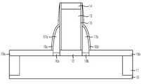
이하, 도 2 내지 도 8을 참조하여, 본 발명의 바람직한 실시예에 따른 2비트를 갖는 비휘발성 메모리 셀의 제조방법을 설명하기로 한다. 여기서, 도 2 내지 도 8은 본 발명의 바람직한 실시예에 따른 2비트 비휘발성 메모리 셀의 제조방법을 설명하기 위하여 도시한 공정단면도들이다. 여기서, 도 2 내지 도 8에 도시된 도면부호 중 동일한 도면부호는 동일한 기능을 하는 동일요소이다.Hereinafter, a method of manufacturing a nonvolatile memory cell having two bits according to a preferred embodiment of the present invention will be described with reference to FIGS. 2 to 8. 2 to 8 are cross-sectional views illustrating a method of manufacturing a 2-bit nonvolatile memory cell according to a preferred embodiment of the present invention. Here, the same reference numerals among the reference numerals shown in FIGS. 2 to 8 are the same elements having the same function.
먼저, 도 2에 도시된 바와 같이, 반도체 기판(10)에 소자 분리막(11)을 형성한다. 이때, 소자 분리막(11)은 STI(Shallow Trench Isolation) 공정 또는 LOCOS(LOCal Oxidation of Silicon) 공정을 실시하여 형성한다. 바람직하게는 집적도 증대를 위해 STI 공정으로 형성한다.First, as shown in FIG. 2, the
이어서, 소자 분리막(11)을 포함한 반도체 기판(10) 전면에 제1 컨트롤 게이트(13)와 기판(10)을 분리시키기 위한 제1 게이트 절연막(12)을 형성한다. 이때, 제1 게이트 절연막(12)은 습식산화공정 또는 건식산화공정을 이용하여 산화막 계열의 물질로 형성한다.Subsequently, a first
이어서, 도 3에 도시된 바와 같이, 제1 절연막(12) 상에 제1 폴리실리콘층(미도시) 및 캡핑층(capping layer, 14)을 증착한다. 이때, 제1 폴리실리콘층은 도프트(doped) 또는 언도프트(un-doped) 실리콘층으로 형성한다. 예컨대, SiH4 또는 SiH4와 PH3를 이용하여 LPCVD(Low Presure Chemical Vapor Depostion) 방식으로 증착한다. 또한, 캡핑층(14)은 하드 마스크(hard mask) 및/또는 반사 방지막(anti-reflection coating layer)을 포함할 수 있으며, 산화막, 질화막 또는 이들이 적층된 적층막으로 형성한다.Next, as shown in FIG. 3, a first polysilicon layer (not shown) and a
이어서, 포토리소그래피(photolithography) 공정을 실시하여 캡핑층(14) 및 제1 폴리실리콘층을 순차적으로 식각하여 제1 컨트롤 게이트(13)를 형성한다.Subsequently, the
이어서, 제1 컨트롤 게이트(13)가 형성된 전체 구조 상부의 단차를 따라 제1 유전체막(15)을 증착한다. 이때, 제1 유전체막(15)은 질화막 계열의 물질로 형성하 여 터널 산화막(11; 도 4 참조)을 형성하기 위한 후속공정시에 그 두께에 영향을 받지 않도록 한다.Subsequently, the
이어서, 포토리소그래피 공정을 이용해 제1 유전체막(15) 및 제1 게이트 절연막(12)을 식각하여 제1 컨트롤 게이트(13) 및 캡핑층(14)의 양측벽에 제1 유전체막(15)을 형성한다. 이러한 포토리소그래피 공정시 캡핑층(14)이 식각장벽층으로 기능하여 제1 컨트롤 게이트(13) 및 캡핑층(14)의 양측벽에 제1 유전체막(15)이 잔류되게 된다.Subsequently, the
이어서, 도 4에 도시된 바와 같이, 산화공정을 실시하여 제1 게이트 절연막(12) 양측으로 노출된 반도체 기판(10) 상에 제1 및 제2 터널 산화막(16a, 16b)을 형성한다. 이때, 제1 및 제2 터널 산화막(16a, 16b)은 제1 게이트 절연막(12)보다 얇게 형성한다.Next, as shown in FIG. 4, an oxidation process is performed to form first and second
이어서, 도 5에 도시된 바와 같이, 제1 터널 산화막(16a) 및 제2 터널 산화막(16b)이 형성된 전체 구조 상부의 단차를 따라 제2 폴리 실리콘층(미도시)을 증착한다.Subsequently, as shown in FIG. 5, a second polysilicon layer (not shown) is deposited along the stepped portion of the entire structure in which the first
이어서, 건식식각공정을 통해 제2 폴리 실리콘층을 식각하여, 제1 유전체막(15)의 양측벽에 제1 및 제2 플로팅 게이트(17a, 17b)를 형성한다. 여기서, 제1 및 제2 플로팅 게이트(17a, 17b)는 제1 컨트롤 게이트(13)를 사이에 두고 서로 분리되며, 제1 유전체막(15)을 통해 제1 컨트롤 게이트(13)의 일부와 각각 중첩된다. 또한, 제1 및 제2 플로팅 게이트(17a, 17b)는 각각 제1 및 제2 터널 산화막(16a, 16b)를 통해 기판(10)과 분리된다.Subsequently, the second polysilicon layer is etched through a dry etching process to form first and second floating
이어서, 제1 플로팅 게이트(17a) 및 제2 플로팅 게이트(17b)가 형성된 전체 구조 상부의 단차를 따라 절연막(18)을 증착한다. 이때, 절연막(18)은 산화막과 질화막이 적층된 구조, 예컨대 ONO(Oxide/Nitride/Oxide) 구조 또는 ON(Oxide/Nitride) 구조로 형성한다.Subsequently, the insulating
이어서, 도 6에 도시된 바와 같이, 건식식각공정을 실시하여 절연막(18), 제1 및 제2 터널 산화막(16a 및 16b)을 식각한다. 이로써, 제1 및 제2 플로팅 게이트(17a, 17b)의 양측에 서로 분리된 제2 및 제3 유전체막(18a, 18b)이 형성된다. 또한, 제2 및 제3 유전체막(18a, 18b)의 양측으로 기판(10)의 일부 영역이 노출된다.Subsequently, as shown in FIG. 6, a dry etching process is performed to etch the insulating
이어서, 습식산화 또는 건식산화공정을 실시하여 제1 및 제2 터널 산화막(16a, 16b)이 제거되어 노출된 기판(10) 상에 제2 및 제3 게이트 절연막(19a, 19b)을 각각 형성한다. 이때, 제2 및 제3 게이트 절연막(19a, 19b)은 제1 게이트 절연막(12)과 동일한 두께로 형성한다.Subsequently, a wet oxidation process or a dry oxidation process is performed to form the second and third
이어서, 도 7에 도시된 바와 같이, 제2 및 제3 게이트 절연막(19a, 19b)이 형성된 결과물 상에 제1 및 제2 플로팅 게이트(17a, 17b)를 감싸도록 제3 폴리 실리콘층(미도시)을 증착한다.Subsequently, as shown in FIG. 7, a third polysilicon layer (not shown) is formed to surround the first and second floating
이어서, CMP(Chemical Mechanical Polishing) 공정을 실시하여 제3 폴리 실리콘층을 평탄화한다. 이로써, 캡핑층(14)이 제거되어 제1 컨트롤 게이트(13)의 상부가 노출된다.Subsequently, the third polysilicon layer is planarized by performing a chemical mechanical polishing (CMP) process. As a result, the
이어서, 포토리소그래피 공정을 실시하여 기판(10)의 일부 영역이 노출되도록 제3 폴리 실리콘층, 제2 절연막(19a) 및 제3 절연막(19b)의 일정 부분을 식각한 다. 이로써, 제2 유전체막(18a)을 사이에 두고 제1 플로팅 게이트(17a)를 감싸는 제2 컨트롤 게이트(20a)가 형성고, 제3 유전체막(18b)을 사이에 두고 제2 플로팅 게이트(17b)를 감싸는 제3 컨트롤 게이트(20b)가 형성된다.Subsequently, a portion of the third polysilicon layer, the second insulating
이어서, 제2 및 제3 컨트롤 게이트(20a 및 20b)가 형성된 전체 구조 상부의 단차를 따라 스페이서용 절연막(미도시)을 증착한 후, 건식식각공정을 실시하여 제2 및 제3 컨트롤 게이트(20a 및 20b) 측벽의 일부에 각각 스페이서(21)를 형성한다.Subsequently, an insulating film for a spacer (not shown) is deposited along the level of the upper part of the entire structure where the second and
이어서, 도 8에 도시된 바와 같이, 스페이서(21)를 마스크로 이용한 고농도 소오스/드레인 이온주입 공정을 실시하여 스페이서(21)의 양측으로 노출된 반도체 기판(10)에 제1 및 제2 접합영역(22a, 22b)을 형성한다.Subsequently, as shown in FIG. 8, the first and second junction regions are exposed to the
이어서, 살리사이드(SALICIDE; Self aligned silicide) 공정을 실시하여 스페이서(21) 형성으로 인해 실리콘이 노출된 영역, 즉 제1 내지 제3 컨트롤 게이트(13, 20a, 20b)와 제1 및 제2 접합영역(22a, 22b) 상부에 금속 실리사이드층(23)을 형성한다. 금속 실리사이드층(23)은 제1 내지 제3 컨트롤 게이트(13, 20a, 20b)를 전기적으로 연결시켜 하나의 컨트롤 게이트로 동작할수 있도록 한다.Subsequently, a self aligned silicide (SALICIDE) process is performed to expose the silicon exposed regions due to the formation of the
한편, 제1 및 제2 플로팅 게이트(17a, 17b)는 제2 및 제3 유전체막(18a, 18b)으로 덮혀 있기 때문에 살리사이드 공정시 제1 및 제2 플로팅 게이트(17a 및 17b)와 제1 내지 제3 컨트롤 게이트(13, 20a, 20b) 간의 숏트(short)를 방지할 수 있다.Meanwhile, since the first and second floating
본 발명의 기술 사상은 상기 바람직한 실시예에 따라 구체적으로 기술되었으 나, 상기한 실시예는 그 설명을 위한 것이며 그 제한을 위한 것이 아님을 주의하여야 한다. 또한, 본 발명의 기술 분야의 통상의 전문가라면 본 발명의 기술 사상의 범위 내에서 다양한 실시예가 가능함을 이해할 수 있을 것이다.Although the technical spirit of the present invention has been described in detail according to the above preferred embodiment, it should be noted that the above-described embodiment is for the purpose of description and not of limitation. In addition, those skilled in the art will understand that various embodiments are possible within the scope of the technical idea of the present invention.
이상에서 설명한 바와 같이, 본 발명에 의하면, 각각 데이터를 저장하는 제1 및 제2 플로팅 게이트의 전후면이 각각 컨트롤 게이트와 중첩되는 구조로 메모리 셀을 형성함으로써 메모리 셀의 커플링비를 증대시켜 프로그램 동작시 비교적 낮은 고전압으로 동작을 수행할 수 있다. 소자의 동작시 메모리 셀의 전력 소모를 감소시킬 수 있다.As described above, according to the present invention, the memory cell is formed in a structure in which front and rear surfaces of the first and second floating gates storing data respectively overlap with the control gate, thereby increasing the coupling ratio of the memory cells, thereby increasing the program operation. The operation can be performed at a relatively low high voltage. It is possible to reduce the power consumption of the memory cell during operation of the device.
Claims (17)
Translated fromKoreanPriority Applications (1)
| Application Number | Priority Date | Filing Date | Title |
|---|---|---|---|
| KR1020050028377AKR100631851B1 (en) | 2005-04-06 | 2005-04-06 | Non-volatile memory cell having 2 bits and manufacturing method thereof |
Applications Claiming Priority (1)
| Application Number | Priority Date | Filing Date | Title |
|---|---|---|---|
| KR1020050028377AKR100631851B1 (en) | 2005-04-06 | 2005-04-06 | Non-volatile memory cell having 2 bits and manufacturing method thereof |
Publications (1)
| Publication Number | Publication Date |
|---|---|
| KR100631851B1true KR100631851B1 (en) | 2006-10-04 |
Family
ID=37622873
Family Applications (1)
| Application Number | Title | Priority Date | Filing Date |
|---|---|---|---|
| KR1020050028377AExpired - Fee RelatedKR100631851B1 (en) | 2005-04-06 | 2005-04-06 | Non-volatile memory cell having 2 bits and manufacturing method thereof |
Country Status (1)
| Country | Link |
|---|---|
| KR (1) | KR100631851B1 (en) |
- 2005
- 2005-04-06KRKR1020050028377Apatent/KR100631851B1/ennot_activeExpired - Fee Related
Similar Documents
| Publication | Publication Date | Title |
|---|---|---|
| US6977200B2 (en) | Method of manufacturing split-gate memory | |
| US7049189B2 (en) | Method of fabricating non-volatile memory cell adapted for integration of devices and for multiple read/write operations | |
| US7355241B2 (en) | Non-volatile memory | |
| US6720219B2 (en) | Split gate flash memory and formation method thereof | |
| JP2000286349A (en) | Semiconductor device and manufacture thereof | |
| KR100546694B1 (en) | Nonvolatile Memory Device and Manufacturing Method Thereof | |
| KR100567757B1 (en) | Manufacturing Method of Semiconductor Device | |
| JP2005026696A (en) | EEPROM device and manufacturing method thereof | |
| JP3947041B2 (en) | Semiconductor device and manufacturing method thereof | |
| US7408219B2 (en) | Nonvolatile semiconductor memory device | |
| KR100631851B1 (en) | Non-volatile memory cell having 2 bits and manufacturing method thereof | |
| KR100683389B1 (en) | Cell transistor of flash memory and manufacturing method thereof | |
| US7537992B2 (en) | Method for manufacturing flash memory device | |
| KR100771418B1 (en) | Method of manufacturing self-aligned flash memory cells | |
| KR100559523B1 (en) | Cell manufacturing method of flash memory device | |
| KR100958627B1 (en) | Flash memory device and manufacturing method thereof | |
| KR100600955B1 (en) | Cell of nonvolatile memory device and method of manufacturing same | |
| KR100663608B1 (en) | Cell manufacturing method of flash memory device | |
| KR20060007176A (en) | Manufacturing method of nonvolatile memory device | |
| US20070147123A1 (en) | Split gate type non-volatile memory device and method of manufacturing the same | |
| KR101051810B1 (en) | Cells of Nonvolatile Memory Devices and Manufacturing Method Thereof | |
| CN101447422A (en) | Method for manufacturing flash memory device | |
| KR20050038750A (en) | Method for manufacturing non-volatile memory device | |
| KR20060077107A (en) | Cell manufacturing method of nonvolatile memory device and semiconductor device manufacturing method using same | |
| KR20080025560A (en) | Nonvolatile Memory Device and Manufacturing Method Thereof |
Legal Events
| Date | Code | Title | Description |
|---|---|---|---|
| A201 | Request for examination | ||
| PA0109 | Patent application | St.27 status event code:A-0-1-A10-A12-nap-PA0109 | |
| PA0201 | Request for examination | St.27 status event code:A-1-2-D10-D11-exm-PA0201 | |
| E902 | Notification of reason for refusal | ||
| PE0902 | Notice of grounds for rejection | St.27 status event code:A-1-2-D10-D21-exm-PE0902 | |
| E701 | Decision to grant or registration of patent right | ||
| PE0701 | Decision of registration | St.27 status event code:A-1-2-D10-D22-exm-PE0701 | |
| GRNT | Written decision to grant | ||
| PR0701 | Registration of establishment | St.27 status event code:A-2-4-F10-F11-exm-PR0701 | |
| PR1002 | Payment of registration fee | St.27 status event code:A-2-2-U10-U11-oth-PR1002 Fee payment year number:1 | |
| PG1601 | Publication of registration | St.27 status event code:A-4-4-Q10-Q13-nap-PG1601 | |
| PR1001 | Payment of annual fee | St.27 status event code:A-4-4-U10-U11-oth-PR1001 Fee payment year number:4 | |
| PR1001 | Payment of annual fee | St.27 status event code:A-4-4-U10-U11-oth-PR1001 Fee payment year number:5 | |
| PR1001 | Payment of annual fee | St.27 status event code:A-4-4-U10-U11-oth-PR1001 Fee payment year number:6 | |
| FPAY | Annual fee payment | Payment date:20120823 Year of fee payment:7 | |
| PR1001 | Payment of annual fee | St.27 status event code:A-4-4-U10-U11-oth-PR1001 Fee payment year number:7 | |
| FPAY | Annual fee payment | Payment date:20130821 Year of fee payment:8 | |
| PR1001 | Payment of annual fee | St.27 status event code:A-4-4-U10-U11-oth-PR1001 Fee payment year number:8 | |
| FPAY | Annual fee payment | Payment date:20140820 Year of fee payment:9 | |
| PR1001 | Payment of annual fee | St.27 status event code:A-4-4-U10-U11-oth-PR1001 Fee payment year number:9 | |
| FPAY | Annual fee payment | Payment date:20150818 Year of fee payment:10 | |
| PR1001 | Payment of annual fee | St.27 status event code:A-4-4-U10-U11-oth-PR1001 Fee payment year number:10 | |
| FPAY | Annual fee payment | Payment date:20160817 Year of fee payment:11 | |
| PR1001 | Payment of annual fee | St.27 status event code:A-4-4-U10-U11-oth-PR1001 Fee payment year number:11 | |
| FPAY | Annual fee payment | Payment date:20170818 Year of fee payment:12 | |
| PR1001 | Payment of annual fee | St.27 status event code:A-4-4-U10-U11-oth-PR1001 Fee payment year number:12 | |
| P22-X000 | Classification modified | St.27 status event code:A-4-4-P10-P22-nap-X000 | |
| FPAY | Annual fee payment | Payment date:20180820 Year of fee payment:13 | |
| PR1001 | Payment of annual fee | St.27 status event code:A-4-4-U10-U11-oth-PR1001 Fee payment year number:13 | |
| PR1001 | Payment of annual fee | St.27 status event code:A-4-4-U10-U11-oth-PR1001 Fee payment year number:14 | |
| PR1001 | Payment of annual fee | St.27 status event code:A-4-4-U10-U11-oth-PR1001 Fee payment year number:15 | |
| PN2301 | Change of applicant | St.27 status event code:A-5-5-R10-R11-asn-PN2301 | |
| PN2301 | Change of applicant | St.27 status event code:A-5-5-R10-R14-asn-PN2301 | |
| R18-X000 | Changes to party contact information recorded | St.27 status event code:A-5-5-R10-R18-oth-X000 | |
| PC1903 | Unpaid annual fee | St.27 status event code:A-4-4-U10-U13-oth-PC1903 Not in force date:20210928 Payment event data comment text:Termination Category : DEFAULT_OF_REGISTRATION_FEE | |
| PC1903 | Unpaid annual fee | St.27 status event code:N-4-6-H10-H13-oth-PC1903 Ip right cessation event data comment text:Termination Category : DEFAULT_OF_REGISTRATION_FEE Not in force date:20210928 | |
| PN2301 | Change of applicant | St.27 status event code:A-5-5-R10-R13-asn-PN2301 St.27 status event code:A-5-5-R10-R11-asn-PN2301 | |
| P22-X000 | Classification modified | St.27 status event code:A-4-4-P10-P22-nap-X000 |