KR100628887B1 - Method for forming a film on a substrate using microwave energy and apparatus for performing the same - Google Patents
Method for forming a film on a substrate using microwave energy and apparatus for performing the sameDownload PDFInfo
- Publication number
- KR100628887B1 KR100628887B1KR1020050009179AKR20050009179AKR100628887B1KR 100628887 B1KR100628887 B1KR 100628887B1KR 1020050009179 AKR1020050009179 AKR 1020050009179AKR 20050009179 AKR20050009179 AKR 20050009179AKR 100628887 B1KR100628887 B1KR 100628887B1
- Authority
- KR
- South Korea
- Prior art keywords
- process chamber
- gas
- film
- boat
- film forming
- Prior art date
- Legal status (The legal status is an assumption and is not a legal conclusion. Google has not performed a legal analysis and makes no representation as to the accuracy of the status listed.)
- Expired - Fee Related
Links
Images


Classifications
- B—PERFORMING OPERATIONS; TRANSPORTING
- B23—MACHINE TOOLS; METAL-WORKING NOT OTHERWISE PROVIDED FOR
- B23K—SOLDERING OR UNSOLDERING; WELDING; CLADDING OR PLATING BY SOLDERING OR WELDING; CUTTING BY APPLYING HEAT LOCALLY, e.g. FLAME CUTTING; WORKING BY LASER BEAM
- B23K10/00—Welding or cutting by means of a plasma
- B23K10/02—Plasma welding
- B23K10/027—Welding for purposes other than joining, e.g. build-up welding
- C—CHEMISTRY; METALLURGY
- C23—COATING METALLIC MATERIAL; COATING MATERIAL WITH METALLIC MATERIAL; CHEMICAL SURFACE TREATMENT; DIFFUSION TREATMENT OF METALLIC MATERIAL; COATING BY VACUUM EVAPORATION, BY SPUTTERING, BY ION IMPLANTATION OR BY CHEMICAL VAPOUR DEPOSITION, IN GENERAL; INHIBITING CORROSION OF METALLIC MATERIAL OR INCRUSTATION IN GENERAL
- C23C—COATING METALLIC MATERIAL; COATING MATERIAL WITH METALLIC MATERIAL; SURFACE TREATMENT OF METALLIC MATERIAL BY DIFFUSION INTO THE SURFACE, BY CHEMICAL CONVERSION OR SUBSTITUTION; COATING BY VACUUM EVAPORATION, BY SPUTTERING, BY ION IMPLANTATION OR BY CHEMICAL VAPOUR DEPOSITION, IN GENERAL
- C23C16/00—Chemical coating by decomposition of gaseous compounds, without leaving reaction products of surface material in the coating, i.e. chemical vapour deposition [CVD] processes
- C23C16/44—Chemical coating by decomposition of gaseous compounds, without leaving reaction products of surface material in the coating, i.e. chemical vapour deposition [CVD] processes characterised by the method of coating
- C23C16/455—Chemical coating by decomposition of gaseous compounds, without leaving reaction products of surface material in the coating, i.e. chemical vapour deposition [CVD] processes characterised by the method of coating characterised by the method used for introducing gases into reaction chamber or for modifying gas flows in reaction chamber
- C23C16/45563—Gas nozzles
- C23C16/45578—Elongated nozzles, tubes with holes
- C—CHEMISTRY; METALLURGY
- C23—COATING METALLIC MATERIAL; COATING MATERIAL WITH METALLIC MATERIAL; CHEMICAL SURFACE TREATMENT; DIFFUSION TREATMENT OF METALLIC MATERIAL; COATING BY VACUUM EVAPORATION, BY SPUTTERING, BY ION IMPLANTATION OR BY CHEMICAL VAPOUR DEPOSITION, IN GENERAL; INHIBITING CORROSION OF METALLIC MATERIAL OR INCRUSTATION IN GENERAL
- C23C—COATING METALLIC MATERIAL; COATING MATERIAL WITH METALLIC MATERIAL; SURFACE TREATMENT OF METALLIC MATERIAL BY DIFFUSION INTO THE SURFACE, BY CHEMICAL CONVERSION OR SUBSTITUTION; COATING BY VACUUM EVAPORATION, BY SPUTTERING, BY ION IMPLANTATION OR BY CHEMICAL VAPOUR DEPOSITION, IN GENERAL
- C23C16/00—Chemical coating by decomposition of gaseous compounds, without leaving reaction products of surface material in the coating, i.e. chemical vapour deposition [CVD] processes
- C23C16/44—Chemical coating by decomposition of gaseous compounds, without leaving reaction products of surface material in the coating, i.e. chemical vapour deposition [CVD] processes characterised by the method of coating
- C23C16/458—Chemical coating by decomposition of gaseous compounds, without leaving reaction products of surface material in the coating, i.e. chemical vapour deposition [CVD] processes characterised by the method of coating characterised by the method used for supporting substrates in the reaction chamber
- C23C16/4582—Rigid and flat substrates, e.g. plates or discs
- C23C16/4583—Rigid and flat substrates, e.g. plates or discs the substrate being supported substantially horizontally
- C23C16/4584—Rigid and flat substrates, e.g. plates or discs the substrate being supported substantially horizontally the substrate being rotated
- C—CHEMISTRY; METALLURGY
- C23—COATING METALLIC MATERIAL; COATING MATERIAL WITH METALLIC MATERIAL; CHEMICAL SURFACE TREATMENT; DIFFUSION TREATMENT OF METALLIC MATERIAL; COATING BY VACUUM EVAPORATION, BY SPUTTERING, BY ION IMPLANTATION OR BY CHEMICAL VAPOUR DEPOSITION, IN GENERAL; INHIBITING CORROSION OF METALLIC MATERIAL OR INCRUSTATION IN GENERAL
- C23C—COATING METALLIC MATERIAL; COATING MATERIAL WITH METALLIC MATERIAL; SURFACE TREATMENT OF METALLIC MATERIAL BY DIFFUSION INTO THE SURFACE, BY CHEMICAL CONVERSION OR SUBSTITUTION; COATING BY VACUUM EVAPORATION, BY SPUTTERING, BY ION IMPLANTATION OR BY CHEMICAL VAPOUR DEPOSITION, IN GENERAL
- C23C16/00—Chemical coating by decomposition of gaseous compounds, without leaving reaction products of surface material in the coating, i.e. chemical vapour deposition [CVD] processes
- C23C16/44—Chemical coating by decomposition of gaseous compounds, without leaving reaction products of surface material in the coating, i.e. chemical vapour deposition [CVD] processes characterised by the method of coating
- C23C16/50—Chemical coating by decomposition of gaseous compounds, without leaving reaction products of surface material in the coating, i.e. chemical vapour deposition [CVD] processes characterised by the method of coating using electric discharges
- C23C16/511—Chemical coating by decomposition of gaseous compounds, without leaving reaction products of surface material in the coating, i.e. chemical vapour deposition [CVD] processes characterised by the method of coating using electric discharges using microwave discharges
- C—CHEMISTRY; METALLURGY
- C23—COATING METALLIC MATERIAL; COATING MATERIAL WITH METALLIC MATERIAL; CHEMICAL SURFACE TREATMENT; DIFFUSION TREATMENT OF METALLIC MATERIAL; COATING BY VACUUM EVAPORATION, BY SPUTTERING, BY ION IMPLANTATION OR BY CHEMICAL VAPOUR DEPOSITION, IN GENERAL; INHIBITING CORROSION OF METALLIC MATERIAL OR INCRUSTATION IN GENERAL
- C23C—COATING METALLIC MATERIAL; COATING MATERIAL WITH METALLIC MATERIAL; SURFACE TREATMENT OF METALLIC MATERIAL BY DIFFUSION INTO THE SURFACE, BY CHEMICAL CONVERSION OR SUBSTITUTION; COATING BY VACUUM EVAPORATION, BY SPUTTERING, BY ION IMPLANTATION OR BY CHEMICAL VAPOUR DEPOSITION, IN GENERAL
- C23C8/00—Solid state diffusion of only non-metal elements into metallic material surfaces; Chemical surface treatment of metallic material by reaction of the surface with a reactive gas, leaving reaction products of surface material in the coating, e.g. conversion coatings, passivation of metals
- C23C8/06—Solid state diffusion of only non-metal elements into metallic material surfaces; Chemical surface treatment of metallic material by reaction of the surface with a reactive gas, leaving reaction products of surface material in the coating, e.g. conversion coatings, passivation of metals using gases
- C23C8/36—Solid state diffusion of only non-metal elements into metallic material surfaces; Chemical surface treatment of metallic material by reaction of the surface with a reactive gas, leaving reaction products of surface material in the coating, e.g. conversion coatings, passivation of metals using gases using ionised gases, e.g. ionitriding
- B—PERFORMING OPERATIONS; TRANSPORTING
- B23—MACHINE TOOLS; METAL-WORKING NOT OTHERWISE PROVIDED FOR
- B23K—SOLDERING OR UNSOLDERING; WELDING; CLADDING OR PLATING BY SOLDERING OR WELDING; CUTTING BY APPLYING HEAT LOCALLY, e.g. FLAME CUTTING; WORKING BY LASER BEAM
- B23K2103/00—Materials to be soldered, welded or cut
- B23K2103/08—Non-ferrous metals or alloys
- B23K2103/14—Titanium or alloys thereof
Landscapes
- Chemical & Material Sciences (AREA)
- Engineering & Computer Science (AREA)
- Mechanical Engineering (AREA)
- Chemical Kinetics & Catalysis (AREA)
- Materials Engineering (AREA)
- Metallurgy (AREA)
- Organic Chemistry (AREA)
- General Chemical & Material Sciences (AREA)
- Physics & Mathematics (AREA)
- Plasma & Fusion (AREA)
- Chemical Vapour Deposition (AREA)
Abstract
Translated fromKoreanDescription
Translated fromKorean도 1은 본 발명의 일 실시예에 따른 막 형성 장치를 설명하기 위한 단면도이다.1 is a cross-sectional view illustrating a film forming apparatus according to an embodiment of the present invention.
도 2는 도 1에 도시된 노즐 파이프와 가스 공급부를 설명하기 위한 개략적인 구성도이다.FIG. 2 is a schematic diagram illustrating a nozzle pipe and a gas supply unit illustrated in FIG. 1.
도 3은 도 1에 마이크로웨이브 안테나를 설명하기 위한 단면도이다.3 is a cross-sectional view illustrating the microwave antenna in FIG. 1.
도 4는 도 1에 도시된 노즐 파이프와 마이크로웨이브 안테나를 설명하기 위한 사시도이다.4 is a perspective view illustrating the nozzle pipe and the microwave antenna shown in FIG. 1.
도 5는 도 4에 도시된 노즐 파이프와 마이크로웨이브 안테나의 다른 예를 설명하기 위한 평면도이다.FIG. 5 is a plan view illustrating another example of the nozzle pipe and the microwave antenna illustrated in FIG. 4.
도 6은 도 4에 도시된 노즐 파이프와 마이크로웨이브 안테나의 또 다른 예를 설명하기 위한 평면도이다.FIG. 6 is a plan view illustrating another example of the nozzle pipe and the microwave antenna illustrated in FIG. 4.
도 7은 도 4에 도시된 노즐 파이프와 마이크로웨이브 안테나의 또 다른 예를 설명하기 위한 평면도이다.FIG. 7 is a plan view illustrating another example of the nozzle pipe and the microwave antenna illustrated in FIG. 4.
도 8은 도 1에 도시된 막 형성 장치를 이용하여 반도체 기판 상에 막을 형성 하는 방법을 설명하기 위한 흐름도이다.FIG. 8 is a flowchart for explaining a method of forming a film on a semiconductor substrate using the film forming apparatus shown in FIG. 1.
* 도면의 주요부분에 대한 부호의 설명 *Explanation of symbols on the main parts of the drawings
10 : 반도체 기판100 : 막 형성 장치10
102 : 공정 챔버104 : 가열로102
106 : 매니폴드108 : 보트106: manifold 108: boat
110 : 리드 부재114 : 턴테이블110: lead member 114: turntable
118 : 회전 구동 유닛120 : 수직 구동 유닛118: rotation drive unit 120: vertical drive unit
132 : 노즐 파이프134 : 마이크로웨이브 안테나132: nozzle pipe 134: microwave antenna
136 : 가스 공급부160 : 도파관136: gas supply unit 160: waveguide
162 : 에너지 소스164 : 사각 튜브162: energy source 164: square tube
166 : 금속층168 : 슬롯166: metal layer 168: slot
본 발명은 기판 상에 막을 형성하기 위한 장치에 관한 것이다. 보다 상세하게는, 소스 가스를 플라즈마 상태로 형성하고, 상기 플라즈마를 이용하여 실리콘웨이퍼와 같은 반도체 기판 상에 막을 형성하기 위한 장치에 관한 것이다.The present invention relates to an apparatus for forming a film on a substrate. More particularly, the present invention relates to an apparatus for forming a source gas in a plasma state and forming a film on a semiconductor substrate such as a silicon wafer using the plasma.
일반적으로, 반도체 장치는 기판으로 사용되는 반도체 웨이퍼에 대한 다수의 공정들을 수행함으로써 제조될 수 있다. 예를 들면, 막 형성 공정은 상기 기판 상에 막을 형성하기 위해 수행되며, 산화 공정은 상기 기판 상에 산화막을 형성하기 위해 또는 상기 기판 상에 형성된 막을 산화시키기 위해 수행되고, 포토리소그래피(photolithography) 공정은 상기 기판 상에 형성된 막을 목적하는 패턴들로 형성하기 위해 수행되고, 평탄화 공정은 상기 기판 상에 형성된 막을 평탄화시키기 위해 수행된다.In general, a semiconductor device can be manufactured by performing a number of processes on a semiconductor wafer used as a substrate. For example, a film forming process is performed to form a film on the substrate, and an oxidation process is performed to form an oxide film on the substrate or to oxidize a film formed on the substrate, and a photolithography process Is performed to form films formed on the substrate into desired patterns, and a planarization process is performed to planarize the film formed on the substrate.
상기 기판 상에는 다양한 막들이 화학 기상 증착(chemical vapor deposition; CVD), 물리 기상 증착(physical vapor deposition; PVD), 원자층 증착(atomic layer deposition; ALD) 등을 통하여 형성된다. 예를 들면, 실리콘 산화막은 반도체 장치의 게이트 절연막, 층간 절연막 등으로 사용되며, CVD 공정을 통해 형성될 수 있다. 실리콘 질화막은 마스크 패턴, 게이트 스페이서 등을 형성하기 위하여 사용되며, CVD 공정을 통해 형성될 수 있다. 또한, 반도체 기판 상에는 금속 배선, 전극 등을 형성하기 위하여 다양한 금속막들이 형성될 수 있으며, 상기 금속막들은 CVD 공정, PVD 공정 또는 ALD 공정을 통해 형성될 수 있다.Various films are formed on the substrate through chemical vapor deposition (CVD), physical vapor deposition (PVD), atomic layer deposition (ALD), and the like. For example, the silicon oxide film is used as a gate insulating film, an interlayer insulating film, or the like of a semiconductor device, and may be formed through a CVD process. The silicon nitride film is used to form a mask pattern, a gate spacer, and the like, and may be formed through a CVD process. In addition, various metal layers may be formed on the semiconductor substrate to form metal lines, electrodes, and the like, and the metal layers may be formed through a CVD process, a PVD process, or an ALD process.
예를 들면, 티타늄막과 티타늄 질화막은 금속 확산을 방지하기 위한 금속 장벽막으로 사용될 수 있다. 상기 티타늄막은 티타늄을 포함하는 소스 가스와 수소와 같은 환원 가스를 이용하는 플라즈마 강화 화학 기상 증착(plasma enhanced chemical vapor deposition; PECVD) 공정을 통해 형성될 수 있으며, 상기 티타늄 질화막은 티타늄을 포함하는 제1소스 가스와 질소를 포함하는 제2소스 가스를 이용하는 저압 화학 기상 증착(low pressure chemical vapor deposition; LPCVD) 공정을 통해 형성될 수 있다.For example, the titanium film and the titanium nitride film can be used as a metal barrier film for preventing metal diffusion. The titanium film may be formed through a plasma enhanced chemical vapor deposition (PECVD) process using a source gas containing titanium and a reducing gas such as hydrogen, and the titanium nitride film is a first source including titanium. It may be formed through a low pressure chemical vapor deposition (LPCVD) process using a second source gas containing gas and nitrogen.
상기 티타늄막을 형성하기 위한 매엽식 PECVD 장치는 샤워 헤드에 RF 전원을 인가함으로써 공정 챔버 내부로 공급된 소스 가스를 플라즈마 상태로 형성할 수 있으며, 배치식 PECVD 장치는 리모트 플라즈마 발생기를 이용하여 소스 가스를 플라즈마 상태로 형성한 후, 상기 플라즈마를 수직형 퍼니스(vertical furnace)와 같은 공정 챔버로 공급할 수 있다.The sheet type PECVD apparatus for forming the titanium film may form a source gas supplied into the process chamber in a plasma state by applying RF power to the shower head, and the batch type PECVD apparatus may use a remote plasma generator to generate the source gas. After forming in a plasma state, the plasma may be supplied to a process chamber, such as a vertical furnace.
그러나, 상기 매엽식 PECVD 장치는 쓰루풋(throughput)이 낮다는 단점을 갖는다. 배치식 PECVD 장치는 상기 매엽식 PECVD 장치에 비하여 높은 쓰루풋을 가지지만, 플라즈마 소스 가스를 공급하는 노즐들이 반도체 기판들의 측면과 인접하여 배치되므로 각각의 반도체 기판에서 막의 두께 균일도가 낮다는 단점을 갖는다. 구체적으로, 각각의 반도체 기판에서 중앙 부위 상의 티타늄막의 두께가 가장자리 부위 상의 티타늄막의 두께보다 얇게 형성된다는 단점을 갖는다.However, the single sheet PECVD apparatus has a disadvantage of low throughput. The batch PECVD apparatus has a higher throughput than the single sheet PECVD apparatus, but has a disadvantage in that the thickness uniformity of the film in each semiconductor substrate is low since the nozzles supplying the plasma source gas are disposed adjacent to the sides of the semiconductor substrates. Specifically, each semiconductor substrate has a disadvantage that the thickness of the titanium film on the center portion is made thinner than the thickness of the titanium film on the edge portion.
상기와 같은 문제점을 해결하기 위한 본 발명의 제1목적은 막의 두께 균일도를 향상시킬 수 있는 배치식 막 형성 방법을 제공하는데 있다.The first object of the present invention for solving the above problems is to provide a batch-type film forming method that can improve the thickness uniformity of the film.
본 발명의 제2목적은 상술한 바와 같은 배치식 막 형성 방법을 수행하는데 적합한 배치식 막 형성 장치를 제공하는데 있다.A second object of the present invention is to provide a batch film forming apparatus suitable for performing the batch film forming method as described above.
상기 제1목적을 달성하기 위한 본 발명의 일 측면에 따른 막 형성 방법은, 공정 챔버 내부에 다수의 기판들을 위치시키는 단계와, 상기 공정 챔버 내부로 상기 기판들 상에 막을 형성하기 위한 제1 공정 가스를 공급하는 단계와, 상기 공급된 제1 공정 가스에 마이크로웨이브 에너지를 인가하여 상기 공급된 제1 공정 가스를 플라즈마 상태로 형성하는 단계와, 상기 플라즈마 상태의 제1 공정 가스를 이용하여 상기 기판들 상에 막을 형성하는 단계와, 상기 공정 챔버 내부로 상기 제1 공정 가스와 질소를 포함하는 제2 공정 가스를 공급하여 상기 기판들 상에 형성된 막 상에 질화막을 인시튜 방식으로 형성하는 단계를 포함할 수 있다.According to an aspect of the present invention, there is provided a method of forming a film, comprising: placing a plurality of substrates in a process chamber, and forming a film on the substrates in the process chamber. Supplying a gas, applying microwave energy to the supplied first process gas to form the supplied first process gas in a plasma state, and using the first process gas in the plasma state Forming a film on the substrate, and supplying a second process gas including the first process gas and nitrogen into the process chamber to form a nitride film in situ on the films formed on the substrates. It may include.
상기 제2목적을 달성하기 위한 본 발명의 다른 측면에 따른 막 형성 장치는, 공정 챔버와, 상기 공정 챔버 내에서 다수의 기판들을 복층(multiple stages)으로 지지하기 위한 보트와, 상기 공정 챔버 내에서 실질적으로 수직 방향으로 연장하며 상기 기판들 상에 막을 형성하기 위하여 공정 가스를 상기 공정 챔버 내부로 공급하는 적어도 하나의 노즐 파이프와, 상기 공정 챔버 내에서 상기 노즐 파이프와 평행한 방향으로 연장하며 상기 공급된 공정 가스를 플라즈마 상태로 형성하기 위하여 마이크로웨이브 에너지를 인가하는 적어도 하나의 마이크로웨이브 안테나를 포함할 수 있다.A film forming apparatus according to another aspect of the present invention for achieving the second object includes a process chamber, a boat for supporting a plurality of substrates in multiple stages in the process chamber, and within the process chamber. At least one nozzle pipe for supplying process gas into the process chamber to extend in a substantially vertical direction and to form a film on the substrates, the supply extending in a direction parallel to the nozzle pipe in the process chamber; It may include at least one microwave antenna for applying microwave energy to form the processed process gas into a plasma state.
이하, 본 발명에 따른 바람직한 실시예를 첨부된 도면을 참조하여 상세하게 설명하면 다음과 같다.Hereinafter, preferred embodiments of the present invention will be described in detail with reference to the accompanying drawings.
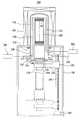
도 1은 본 발명의 일 실시예에 따른 막 형성 장치를 설명하기 위한 단면도이고, 도 2는 도 1에 도시된 노즐 파이프와 가스 공급부를 설명하기 위한 개략적인 구성도이며, 도 3은 도 1에 마이크로웨이브 안테나를 설명하기 위한 단면도이다.1 is a cross-sectional view illustrating a film forming apparatus according to an embodiment of the present invention, FIG. 2 is a schematic configuration diagram illustrating the nozzle pipe and the gas supply unit shown in FIG. 1, and FIG. It is sectional drawing for demonstrating a microwave antenna.
도 1에 도시된 바와 같은 상기 본 발명의 일 실시예에 따른 막 형성 장치(100)는 실리콘웨이퍼와 같은 반도체 기판(10) 상에 막을 형성하는 공정, 예를 들면, 화학 기상 증착 공정, 원자층 증착 공정 등을 수행하는데 바람직하게 사용될 수 있다.The
도 1을 참조하면, 공정 챔버(102)는 배치 타입 수직형 반응로(reaction furnace)를 포함한다. 구체적으로, 상기 공정 챔버(102)는 수직 방향으로 연장하며, 하부가 개방된 실린더 형상을 갖고, 석영(quartz)으로 이루어질 수 있다. 상기 공정 챔버(102)를 가열하기 위한 가열로(heating furnace, 104)는 공정 챔버(102)를 감싸도록 배치되어 있으며, 상기 공정 챔버(102)의 하부에는 금속 재질로 이루어지며 상부 및 하부가 개방된 실린더형 매니폴드(106)가 결합되어 있다.Referring to FIG. 1,
보트(108)는 다수의 반도체 기판(10)을 수직 방향으로 소정 간격을 두고 지지하며, 매니폴드(106)의 하부 개구를 통해 공정 챔버(102)의 내부로 반입된다. 상기 하부 개구는 반도체 기판들(10)이 공정 챔버(102)로 로딩된 후 리드 부재(lid member, 110)에 의해 닫힌다. 상기 공정 챔버(102)와 매니폴드(106) 사이 및 매니폴드(106)와 리드 부재(110) 사이에는 각각 밀봉을 제공하기 위한 밀봉 부재들(seal member, 112)이 개재되어 있다.The
상기 보트(108)는 턴테이블(turntable, 114) 상에 배치되며, 상기 턴테이블(114)은 회전축(116)의 상부에 결합된다. 회전 구동 유닛(118)은 수직 구동 유닛(120)의 수평 암(122)의 하부에 장착되며, 상기 리드 부재(110)는 상기 수직 구동 유닛(120)의 수평 암(122)의 상부에 배치되어 있다.The
한편, 상기 회전축(116)과 리드 부재(110) 사이의 갭을 통한 누설(leakage)을 방지하기 위한 기계적 밀봉부(mechanical seal, 124)가 상기 리드 부재(110)와 수평 암(122) 사이에 배치되며, 상기 회전축(116)은 상기 리드 부재(110), 기계적 밀봉부(124) 및 수평 암(122)을 통하여 상기 턴테이블(114)과 회전 구동 유닛(118)과 연결한다. Meanwhile, a
상기 매니폴드(106)는 로드락 챔버(또는 트랜스퍼 챔버, 126)의 상부에 배치되며, 보트(108)는 공정 챔버(102)와 로드락 챔버(126) 사이에서 수직 방향으로 이동한다.The
상기 수직 구동 유닛(120)은 수평 암(122)과 수평 암(122)을 수직 방향으로 이동시키기 위한 구동력을 제공하는 수직 구동부(128)와 상기 구동력을 전달하기 위한 구동축(130)을 포함한다. 상기 수직 구동부(128)는 제1모터를 포함하여 구성될 수 있으며, 상기 구동축(130)으로는 상기 제1모터로부터 제공되는 회전력에 의해 회전하는 리드 스크루(lead screw)가 사용될 수 있다. 상기 수평 암(122)은 상기 구동축(130)과 결합되며, 구동축(130)의 회전에 의해 수직 방향으로 이동한다.The
상기 회전 구동 유닛(118)은 제2모터를 포함하여 구성될 수 있다. 상세히 도시되지는 않았으나, 상기 제2모터부터 제공된 회전력은 상기 제2모터와 연결된 구동 기어와 상기 회전축(116)과 연결된 종동 기어 및 상기 구동 기어와 종동 기어 사이를 연결하는 타이밍 벨트를 통해 회전축(116)으로 전달될 수 있다. 그러나, 상기 구동 기어와 종동 기어는 직접적으로 연결될 수도 있다.The
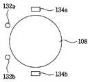
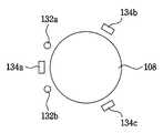
공정 챔버(102)의 측벽과 보트(108) 사이에는 공정 가스를 공급하기 위한 노즐 파이프들(132)이 배치되며, 마이크로웨이브 안테나(134)는 공정 챔버(102) 내부로 공급된 공정 가스를 플라즈마 상태로 여기시키기 위한 마이크로웨이브 에너지를 인가하기 위하여 상기 보트(108)를 사이에 두고 상기 노즐 파이프들(132)과 마주하여 배치되어 있다.
도 2를 참조하면, 가스 공급부(136)는 보트(108)에 의해 공정 챔버(102) 내 에 위치된 다수의 반도체 기판들(10) 상에 각각 막을 형성하기 위한 공정 가스들과 공정 챔버(102) 내부를 퍼지하기 위한 퍼지 가스를 공정 챔버(102) 내부로 공급한다.Referring to FIG. 2, the
예를 들면, 상기 반도체 기판들(10) 상에 티타늄막을 형성하는 경우, 가스 공급부(136)는 상기 공정 챔버(102) 내부로 티타늄 전구체를 포함하는 제1소스 가스와 환원 가스로 사용되는 수소(H2) 가스를 공급한다. 이와 다르게, 상기 반도체 기판들(10) 상에 티타늄 질화막을 형성하는 경우, 공정 챔버(102) 내부로 티타늄 전구체를 포함하는 제1소스 가스와 질소를 포함하는 제2소스 가스를 공급한다.For example, in the case of forming a titanium film on the
구체적으로, 상기 가스 공급부(136)는, 소스 가스들을 공급하기 위한 제1가스 공급부(138) 및 제2가스 공급부(140)와, 상기 환원 가스를 공급하기 위한 제3가스 공급부(142)와, 상기 퍼지 가스를 공급하기 위한 제4가스 공급부(144)를 포함할 수 있다.Specifically, the
상기 제1소스 가스로는 TiCl4이 사용될 수 있으며, 이밖에도 테트라 터셔리 부톡시 티타늄(tetra tertiary butoxy titanium, Ti(OtBu)4), 테트라키스 디메틸 아미노 티타늄(tetrakis dimethyl amino titanium; TDMAT, Ti(NMe2)4), 테트라키스 디에틸 아미노 티타늄(tetrakis diethyl amino titanium; TDEAT, Ti(NEt2)4), 테트라키스 에틸메틸 아미노 티타늄(tetrakis ethylmethyl amino titanium, Ti(NEtMe)4) 등이 사용될 수 있다. 상기 제2소스 가스로는 NH3 가스가 사용될 수 있다. 상기 퍼 지 가스 및 상기 소스 가스들을 운반하기 위한 캐리어 가스들로는 아르곤(Ar) 가스 또는 질소(N2) 가스가 각각 사용될 수 있다.TiCl4 may be used as the first source gas, in addition to tetra tertiary butoxy titanium (Ti (OtBu)4 ), tetrakis dimethyl amino titanium; TDMAT, Ti (NMe2)4 ), tetrakis diethyl amino titanium (TDEAT, Ti (NEt2 )4 ), tetrakis ethylmethyl amino titanium, Ti (NEtMe)4 ), and the like. NH3 gas may be used as the second source gas. Argon (Ar) gas or nitrogen (N2 ) gas may be used as carrier gases for carrying the purge gas and the source gases, respectively.
공정 챔버(102) 내에는 한 쌍의 노즐 파이프들(132a, 132b)이 배치되어 있으며, 매니폴드(106)를 통해 가스 공급부(136)와 연결된다. 구체적으로, 제1가스 공급부(138)는 제1가스 공급 배관(146a)을 통해 매니폴드(106) 내에 배치된 제1노즐 파이프(132a)의 하단부에 연결되어 있으며, 제2가스 공급부(140)는 제2가스 공급 배관(146b)을 통해 매니폴드(106) 내에 배치된 제2노즐 파이프(132b)의 하단부에 연결되어 있다.A pair of
상기 제1가스 공급부(138)는 상기 제1캐리어 가스를 공급하기 위한 제1저장부(148a)와, 상기 제1캐리어 가스의 공급 유량을 조절하기 위한 제1밸브(150a)와, 액상의 티타늄 전구체를 저장하기 위한 제2저장부(148b)와, 상기 액상의 티타늄 전구체의 공급 유량을 조절하기 위한 액체 질량 유량 제어기(liquid mass flow controller, 152)와, 상기 액상의 티타늄 전구체를 기화시키기 위한 기화기(vaporizer, 154)를 포함하여 구성될 수 있다. 이와는 다르게, 상기 제1가스 공급부(138)는 액상의 티타늄 전구체를 기화시키기 위한 버블러를 포함하여 구성될 수도 있다.The first
구체적으로, 제1저장부(148a)와 기화기(154)는 제1연결 배관(156a)을 통해 연결되며, 제1연결 배관(156a)에는 상기 제1밸브(150a)가 설치되어 있다. 제2저장부(148b)와 기화기(154)는 제2연결 배관(156b)을 통해 연결되며, 제2연결 배관 (156b)에는 상기 액체 질량 유량 제어기(152)가 설치되어 있다.Specifically, the
상기 액상의 티타늄 전구체는 상기 기화기(154)의 내부에서 기화되며, 기화된 티타늄 전구체 가스와 상기 제1캐리어 가스는 제1가스 공급 배관(146a)과 제1노즐 파이프(132a)의 제1노즐들을 통해 공정 챔버(102)의 내부로 공급된다.The liquid titanium precursor is vaporized in the vaporizer 154, and the vaporized titanium precursor gas and the first carrier gas may be formed by the first nozzles of the first
제2가스 공급부(140)는 상기 제2소스 가스로 사용되는 NH3 가스를 반도체 기판들(10) 상으로 공급하기 위하여 제2가스 공급 배관(146b)을 통해 제2노즐 파이프(132b)에 연결되어 있다. 구체적으로, 제2가스 공급 배관(146b)은 제2노즐 파이프와 제2캐리어 가스를 제공하기 위한 제3저장부(148c) 사이를 연결하며, 제2가스 공급부(140)는 제3연결 배관(156c)을 통해 제2가스 공급 배관(146b)과 연결되어 있다. 상기 제2가스 공급 배관(146b)에는 상기 제2캐리어 가스의 공급 유량을 조절하기 위한 제2밸브(150b)가 설치되어 있으며, 제3연결 배관(156c)에는 상기 제2소스 가스의 공급 유량을 조절하기 위한 제3밸브(150c)가 설치되어 있다.The second
상기 제3가스 공급부(142)는 상기 환원 가스를 공급하기 위하여 제4연결 배관(156d)을 통해 제2가스 공급 배관(146b)과 연결되어 있다. 상기 제4연결 배관(156d)에는 상기 환원 가스의 공급 유량을 조절하기 위한 제4밸브(150d)가 설치되어 있다. The third
제4가스 공급부(144)는 퍼지 가스를 제공하기 위하여 상기 제5연결 배관(156e)과 제6연결 배관(156f)을 통해 제1가스 공급 배관(146a)과 제2가스 공급 배관(146b)에 각각 연결되어 있다. 상기 제5연결 배관(156e)에는 제1노즐 파이프 (132a)를 통해 공급되는 퍼지 가스의 유량을 조절하기 위한 제5밸브(150e)가 설치되며, 제6연결 배관(156f)에는 제2노즐 파이프(132b)를 통해 공급되는 퍼지 가스의 유량을 조절하기 위한 제6밸브(150f)가 설치된다.The fourth
한편, 도시된 바와 같이, 제1가스 공급 배관(146a)에는 상기 제1소스 가스 및 제1캐리어 가스의 제1혼합 가스의 공급 유량을 조절하기 위한 제1질량 유량 제어기(158a, mass flow controller; MFC)가 설치될 수 있으며, 제2가스 공급 배관(146b)에는 상기 제2소스 가스와 제2캐리어 가스의 제2혼합 가스 및 상기 환원 가스와 상기 제2캐리어 가스의 제3혼합 가스의 공급 유량을 조절하기 위한 제2질량 유량 제어기(158b)가 설치될 수 있다.On the other hand, as shown, the first
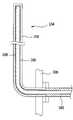
도 3을 참조하면, 상기 마이크로웨이브 안테나(134)는 실질적으로 수직 방향으로 연장하며, 매니폴드(106) 내에서 직각으로 절곡되어 매니폴드(106)를 통해 마이크로웨이브를 전달하기 위한 도파관(160)과 연결된다. 상기 도파관(160)은 마이크로웨이브 에너지를 발생시키기 위한 에너지 소스(162)와 연결되어 있다. 상기 에너지 소스(162)로는 마이크로웨이브를 발생시키기 위한 마이크로웨이브 파워 소스가 사용될 수 있으며, 상기 마이크로웨이브 파워 소스는 2.45GHz의 주파수를 갖는 마이크로웨이브를 발생시키기 위한 발진기와, 상기 발진기에 의해 발진된 마이크로웨이브를 증폭시키기 위한 증폭기를 포함할 수 있다.Referring to FIG. 3, the
상기 마이크로웨이브 안테나(134)로는 슬롯 안테나가 사용될 수 있다. 구체적으로, 상기 마이크로웨이브 안테나(134)는 절연체로 이루어지며 밀폐된 단부를 갖는 사각 튜브(164)와, 상기 사각 튜브(164)의 내면들 상에 형성된 금속층(166)을 포함할 수 있다. 상기 절연체로는 석영이 사용될 수 있으며, 상기 금속층(166)으로는 구리가 사용될 수 있다. 상기 금속층(166)에는 상기 마이크로웨이브 에너지를 공정 챔버(102) 내부로 인가하기 위한 다수의 슬롯들(168)이 공정 챔버(102)의 중심축을 향하여 형성되어 있으며, 상기 마이크로웨이브 에너지는 상기 슬롯들(168)과 사각 튜브(164)의 측벽을 통해 공정 챔버(102) 내부로 공급된 공정 가스들에 인가된다.A slot antenna may be used as the
도 4는 도 1에 도시된 노즐 파이프와 마이크로웨이브 안테나를 설명하기 위한 사시도이다.4 is a perspective view illustrating the nozzle pipe and the microwave antenna shown in FIG. 1.
도 4를 참조하면, 제1노즐 파이프(132a)는 보트(108)에 적재된 반도체 기판(10)들과 인접하게 배치되어 제1가스 공급 배관(132a)으로부터 수직 상방으로 연장하며, 제1소스 가스를 분사하기 위한 다수의 제1노즐들(170a)을 갖는다. 상기 제1노즐들(170a)은 보트(108)에 지지된 반도체 기판들(10)의 표면들을 따라 상기 제1소스 가스가 흐르도록 상기 제1노즐 파이프(132a)의 연장 방향을 따라 일정 간격으로 제1노즐 파이프(132a)의 측면을 관통하여 형성되어 있다. 부언하면, 상기 제1노즐들(170a)은 상기 반도체 기판들(10) 사이의 공간들로 제1소스 가스를 공급하며, 상기 제1소스 가스는 상기 제1노즐들(170a)을 통해 반도체 기판들(10)의 중심들을 향하여 분사된다.Referring to FIG. 4, the
제2노즐 파이프(132b)는 상기 보트(108)에 적재된 반도체 기판들(10)과 인접하게 배치되어 상기 제1노즐 파이프(132a)와 평행하게 연장하며, 제2소스 가스 또는 환원 가스를 분사하기 위한 다수의 제2노즐들(170b)을 갖는다. 상기 제2노즐들 (170b)은 보트(108)에 지지된 반도체 기판들(10)의 표면을 따라 상기 제2소스 가스 또는 환원 가스가 흐르도록 상기 제2노즐 파이프(132b)의 연장 방향을 따라 일정 간격으로 제2노즐 파이프(132b)의 측면을 관통하여 형성되어 있다. 부언하면, 상기 제2노즐들(170b)은 상기 반도체 기판들(10) 사이의 공간들로 제2소스 가스를 공급하며, 상기 제2소스 가스는 상기 제2노즐들(170b)을 통해 반도체 기판들(10)의 중심들을 향하여 분사된다.The
상기 제1소스 가스의 분사 방향과 상기 제2소스 가스 또는 상기 환원 가스의 분사 방향이 이루는 사이각은 약 20°내지 80°정도일 수 있으며, 상기 제1노즐 파이프(132a) 및 제2노즐 파이프(132b)는 반도체 기판들(10)의 중심축으로부터 동일한 거리에 각각 위치될 수 있다.An angle formed between an injection direction of the first source gas and an injection direction of the second source gas or the reducing gas may be about 20 ° to about 80 °, and the
공정 챔버(102) 내부로 공급된 가스들은 상기 마이크로웨이브 안테나(134)로부터 인가된 마이크로웨이브 에너지에 의해 플라즈마 상태로 여기된다. 상기와 같이 마이크로웨이브 에너지에 의해 공정 챔버(102) 내에서 플라즈마가 형성되므로 각각의 반도체 기판들(10) 상에는 균일한 두께를 갖는 막들이 형성될 수 있다.Gases supplied into the
도시된 바에 의하면, 하나의 마이크로웨이브 안테나(134)가 노즐 파이프들(132a, 132b)과 마주하여 배치되어 있다. 그러나, 도 5에 도시된 바와 같이, 하나의 마이크로웨이브 안테나(134)가 노즐 파이프들(132a, 132b) 사이에 배치될 수도 있다. 또한, 도 6 및 도 7에 도시된 바와 같이, 한 쌍의 마이크로웨이브 안테나들(134a, 134b)이 보트(108)를 사이에 두고 서로 마주하여 배치될 수도 있으며, 다수의 마이크로웨이브 안테나들(134a, 134b, 134c)이 보트(108)를 중심으로 방사상으 로 배치될 수도 있다.As shown, one
다시 도 1을 참조하면, 상기 공정 챔버(102)를 진공 배기하기 위한 진공 펌프(미도시)는 진공 배관(172) 및 격리 밸브(isolation valve, 미도시)를 통해 매니폴드(106)와 연결되어 있으며, 가열로(104)는 공정 챔버(102)의 측벽 및 천정과 인접하게 배치되어 있다.Referring back to FIG. 1, a vacuum pump (not shown) for evacuating the
한편, 매니폴드(106)의 내부 공간은 공정 챔버(102)의 내부 공간에 비하여 상대적으로 온도가 낮게 형성될 수 있다. 이러한 온도 차이를 보상하기 위하여 리드 부재(110) 내에는 히터(174)가 구비된다. 즉, 상기 히터(174)는 매니폴드(106) 내부를 가열함으로써 공정 챔버(102)의 내부와 매니폴드(106)의 내부의 온도 분포가 균일하게 형성될 수 있도록 한다. 상기 히터(174)로는 전기 저항 열선이 사용될 수 있다. 그러나, 상기 히터(174)는 매니폴드(106)의 측벽 내에 배치될 수도 있으며, 매니폴드(106)의 내측면 상에 배치될 수도 있다.On the other hand, the internal space of the manifold 106 may be formed at a lower temperature than the internal space of the
티타늄막 및 티타늄 질화막의 형성Formation of titanium film and titanium nitride film
도 8은 도 1에 도시된 막 형성 장치를 이용하여 반도체 기판 상에 막을 형성하는 방법을 설명하기 위한 흐름도이다.8 is a flowchart for explaining a method of forming a film on a semiconductor substrate using the film forming apparatus shown in FIG. 1.
첨부된 도면들을 참조하여 다수의 반도체 기판들(10) 상에 오믹 콘택(ohmic contact)을 형성하기 위한 티타늄막 및 금속 장벽막으로 사용되는 티타늄 질화막을 각각 형성하는 방법을 설명하면 다음과 같다.Referring to the accompanying drawings, a method of forming a titanium film and a titanium nitride film used as a metal barrier film for forming ohmic contacts on a plurality of
먼저, 반도체 기판들(10)을 공정 챔버(102) 내에 위치시킨다. (단계 S100) 구체적으로, 반도체 기판들(10)은 수직 방향으로 일정 간격을 두고 보트(108)에 적재되며, 각각의 반도체 기판들(10)은 수평 방향으로 유지된다. 상기 보트(108)는 수직 구동 유닛(120)의 동작에 의해 매니폴드(106)를 통해 공정 챔버(102) 내부로 이동된다.First, the
상기 반도체 기판(10) 상에는 반도체 장치를 구성하는 반도체 구조물들이 형성되어 있을 수 있다. 예를 들면, 상기 반도체 구조물들은 트랜지스터와 커패시터의 하부 전극 및 유전막을 포함할 수 있다. 상기 트랜지스터는 게이트 구조물과 소스/드레인으로 기능하는 불순물 영역들을 포함하며, 상기 커패시터의 하부 전극은 상기 불순물 영역들 중 하나에 연결된다. 상기 유전막은 상기 커패시터의 하부 전극 상에 형성되어 있다. 상기 하부 전극은 도프트 폴리실리콘으로 이루어질 수 있으며, 상기 유전막은 하프늄 산화물(HfO2)로 이루어질 수 있다.The semiconductor structures constituting the semiconductor device may be formed on the
공정 챔버(102) 내부로 상기 제1소스 가스를 제1노즐들(170a)을 통하여 공급하고, 상기 환원 가스를 제2노즐들(170b)을 통해 공급한다. (단계 S110) 상기 제1소스 가스로는 TiCl4 가스가 사용될 수 있으며, 상기 환원 가스로는 H2 가스가 사용될 수 있다.The first source gas is supplied into the
공정 챔버(102) 내부로 공급된 제1소스 가스와 환원 가스에 마이크로웨이브 에너지를 인가함으로써 상기 제1소스 가스와 환원 가스를 플라즈마 상태로 형성한다. (단계 S120) 구체적으로, 상기 공정 챔버(102) 내에 배치된 마이크로웨이브 안테나(134)를 통해 상기 공급된 가스들에 2.45GHz의 마이크로웨이브 에너지를 인가 한다.Microwave energy is applied to the first source gas and the reducing gas supplied into the
상기 플라즈마 가스를 이용하여 상기 반도체 기판들(10) 상에 티타늄막들을 형성한다. (단계 S130)Titanium films are formed on the
목적하는 두께를 갖는 티타늄막의 형성이 종료되면, 공정 챔버(102) 내부로 퍼지 가스를 공급하여 공정 챔버(102) 내부를 일차 퍼지시킨다. (단계 S140)When the formation of the titanium film having the desired thickness is finished, a purge gas is supplied into the
공정 챔버(102) 내부로 상기 제1소스 가스와 제2소스 가스를 제1노즐들(170a) 및 제2노즐들(170b)을 통해 각각 공급하여 상기 티타늄막들 상에 티타늄 질화막들을 형성한다. (단계 S150) 상기 제1소스 가스로는 TiCl4 가스가 사용될 수 있으며, 상기 제2소스 가스로는 NH3 가스가 사용될 수 있다.Titanium nitride layers are formed on the titanium layers by supplying the first source gas and the second source gas into the
목적하는 두께를 갖는 티타늄 질화막의 형성이 종료되면, 공정 챔버(102) 내부로 퍼지 가스를 공급하여 공정 챔버(102) 내부를 이차 퍼지시킨다. (단계 S160)When the formation of the titanium nitride film having the desired thickness is finished, a purge gas is supplied into the
상기 반도체 기판들(10)을 공정 챔버(102)로부터 언로딩시킨다. (단계 S170) 상기 보트(108)는 수직 구동 유닛(120)의 동작에 의해 공정 챔버(102)로부터 로드락 챔버(126)로 반출된다.The semiconductor substrates 10 are unloaded from the
상기와 같은 본 발명의 일 실시예에 따르면, 다수의 반도체 기판들을 수용하는 공정 챔버 내부로 공급된 공정 가스에 마이크로웨이브 에너지를 인가함으로써 균일한 두께를 갖는 막을 형성할 수 있다.According to one embodiment of the present invention as described above, it is possible to form a film having a uniform thickness by applying microwave energy to the process gas supplied into the process chamber containing a plurality of semiconductor substrates.
또한, 상기 막 형성 장치는 마이크로웨이브를 이용하는 플라즈마 강화 화학 기상 증착 공정과 저압 화학 기상 증착 공정을 인시튜로 수행할 수 있다. 예를 들면, 상기 막 형성 장치를 이용하여 반도체 기판 상에 티타늄막을 형성하는 경우, 후속하여 티타늄 질화막을 인시튜 방식으로 형성할 수 있다.In addition, the film forming apparatus may perform a plasma enhanced chemical vapor deposition process using a microwave and a low pressure chemical vapor deposition process in situ. For example, when the titanium film is formed on the semiconductor substrate using the film forming apparatus, the titanium nitride film may be subsequently formed in-situ.
상기에서는 본 발명의 바람직한 실시예를 참조하여 설명하였지만, 해당 기술 분야의 숙련된 당업자는 하기의 특허 청구의 범위에 기재된 본 발명의 사상 및 영역으로부터 벗어나지 않는 범위 내에서 본 발명을 다양하게 수정 및 변경시킬 수 있음을 이해할 수 있을 것이다.Although described above with reference to a preferred embodiment of the present invention, those skilled in the art will be variously modified and changed within the scope of the invention without departing from the spirit and scope of the invention described in the claims below I can understand that you can.
Claims (22)
Translated fromKoreanPriority Applications (2)
| Application Number | Priority Date | Filing Date | Title |
|---|---|---|---|
| KR1020050009179AKR100628887B1 (en) | 2005-02-01 | 2005-02-01 | Method for forming a film on a substrate using microwave energy and apparatus for performing the same |
| US11/346,597US20060175304A1 (en) | 2005-02-01 | 2006-02-01 | Method of forming layers on substrates using microwave energy and apparatus for performing the same |
Applications Claiming Priority (1)
| Application Number | Priority Date | Filing Date | Title |
|---|---|---|---|
| KR1020050009179AKR100628887B1 (en) | 2005-02-01 | 2005-02-01 | Method for forming a film on a substrate using microwave energy and apparatus for performing the same |
Publications (2)
| Publication Number | Publication Date |
|---|---|
| KR20060088326A KR20060088326A (en) | 2006-08-04 |
| KR100628887B1true KR100628887B1 (en) | 2006-09-26 |
Family
ID=36778897
Family Applications (1)
| Application Number | Title | Priority Date | Filing Date |
|---|---|---|---|
| KR1020050009179AExpired - Fee RelatedKR100628887B1 (en) | 2005-02-01 | 2005-02-01 | Method for forming a film on a substrate using microwave energy and apparatus for performing the same |
Country Status (2)
| Country | Link |
|---|---|
| US (1) | US20060175304A1 (en) |
| KR (1) | KR100628887B1 (en) |
Cited By (1)
| Publication number | Priority date | Publication date | Assignee | Title |
|---|---|---|---|---|
| KR102467388B1 (en)* | 2021-05-10 | 2022-11-16 | 피코순 오와이 | Substrate processing apparatus and method |
Families Citing this family (7)
| Publication number | Priority date | Publication date | Assignee | Title |
|---|---|---|---|---|
| KR101025323B1 (en)* | 2004-01-13 | 2011-03-29 | 가부시키가이샤 아루박 | Etching Apparatus and Etching Method |
| TWI364126B (en)* | 2007-11-23 | 2012-05-11 | Ind Tech Res Inst | Plasma assisted apparatus for forming organic film |
| US8007275B2 (en)* | 2008-01-25 | 2011-08-30 | Micron Technology, Inc. | Methods and apparatuses for heating semiconductor wafers |
| JP5087657B2 (en)* | 2009-08-04 | 2012-12-05 | 株式会社日立国際電気 | Semiconductor device manufacturing method and substrate processing apparatus |
| WO2012021325A2 (en)* | 2010-08-12 | 2012-02-16 | Ovshinsky Innovation, Llc | Plasma deposition of amorphous semiconductors at microwave frequencies |
| JP6294151B2 (en)* | 2014-05-12 | 2018-03-14 | 東京エレクトロン株式会社 | Deposition method |
| JP7729705B2 (en)* | 2021-08-23 | 2025-08-26 | 東京エレクトロン株式会社 | Semiconductor manufacturing equipment and semiconductor device manufacturing method |
Citations (2)
| Publication number | Priority date | Publication date | Assignee | Title |
|---|---|---|---|---|
| JPH10158846A (en)* | 1996-12-05 | 1998-06-16 | Canon Inc | Batch type microwave plasma processing apparatus and processing method |
| JPH10321607A (en) | 1997-05-21 | 1998-12-04 | Ricoh Co Ltd | Plasma processing equipment |
Family Cites Families (6)
| Publication number | Priority date | Publication date | Assignee | Title |
|---|---|---|---|---|
| US3518688A (en)* | 1965-11-22 | 1970-06-30 | Itt | Microwave strip transmission line adapted for integral slot antenna |
| JPS5673539A (en)* | 1979-11-22 | 1981-06-18 | Toshiba Corp | Surface treating apparatus of microwave plasma |
| JPH0633246A (en)* | 1992-07-21 | 1994-02-08 | Canon Inc | Formation of deposited film and deposited film forming device |
| JPH0786174A (en)* | 1993-09-16 | 1995-03-31 | Tokyo Electron Ltd | Film deposition system |
| AU7644600A (en)* | 1999-10-13 | 2001-04-23 | Centrotherm Elektrische Anlagen Gmbh And Co. | Method and device for producing solar cells |
| JP2008521261A (en)* | 2004-11-22 | 2008-06-19 | アプライド マテリアルズ インコーポレイテッド | Substrate processing apparatus using batch processing chamber |
- 2005
- 2005-02-01KRKR1020050009179Apatent/KR100628887B1/ennot_activeExpired - Fee Related
- 2006
- 2006-02-01USUS11/346,597patent/US20060175304A1/ennot_activeAbandoned
Patent Citations (2)
| Publication number | Priority date | Publication date | Assignee | Title |
|---|---|---|---|---|
| JPH10158846A (en)* | 1996-12-05 | 1998-06-16 | Canon Inc | Batch type microwave plasma processing apparatus and processing method |
| JPH10321607A (en) | 1997-05-21 | 1998-12-04 | Ricoh Co Ltd | Plasma processing equipment |
Cited By (1)
| Publication number | Priority date | Publication date | Assignee | Title |
|---|---|---|---|---|
| KR102467388B1 (en)* | 2021-05-10 | 2022-11-16 | 피코순 오와이 | Substrate processing apparatus and method |
Also Published As
| Publication number | Publication date |
|---|---|
| KR20060088326A (en) | 2006-08-04 |
| US20060175304A1 (en) | 2006-08-10 |
Similar Documents
| Publication | Publication Date | Title |
|---|---|---|
| KR101610773B1 (en) | Method for manufacturing thin film and apparatus for the same | |
| JP4713241B2 (en) | High speed atomic layer deposition apparatus and method of use | |
| JP4174424B2 (en) | Method for depositing a refractory metal layer using a series of deposition techniques | |
| JP4382750B2 (en) | CVD method for forming a silicon nitride film on a substrate to be processed | |
| US7825039B2 (en) | Vertical plasma processing method for forming silicon containing film | |
| US12157945B2 (en) | Thermal atomic layer deposition of silicon-containing films | |
| US20140023794A1 (en) | Method And Apparatus For Low Temperature ALD Deposition | |
| KR100724571B1 (en) | Plasma processing apparatus having in-situ cleaning function and its use method | |
| EP1703552A2 (en) | Method of forming non-conformal layers | |
| US10224185B2 (en) | Substrate processing apparatus | |
| CN101562133A (en) | Film formation method and apparatus for forming silicon-containing insulating film doped with metal | |
| KR20060103128A (en) | Deposition apparatus, deposition method and storage medium | |
| KR100636037B1 (en) | Titanium nitride film forming method and apparatus for performing the same | |
| US20060175304A1 (en) | Method of forming layers on substrates using microwave energy and apparatus for performing the same | |
| KR100636036B1 (en) | Titanium nitride film forming method and apparatus for performing the same | |
| US20230377953A1 (en) | Substrate processing method and substrate processing apparatus | |
| TWI887480B (en) | Deposition of silicon boron nitride films | |
| KR101970378B1 (en) | In-situ hydroxylation apparatus | |
| KR20230134554A (en) | Gap filling process using pulsed HFRF (HIGH-FREQUENCY RADIO-FREQUENCY) plasma | |
| KR20240090473A (en) | Methods of Forming Metal Nitride Films | |
| KR100600051B1 (en) | Atomic layer deposition equipment and ternary thin film formation method using the same | |
| TW202444945A (en) | Feature fill using inhibition | |
| US20200303183A1 (en) | High selectivity atomic later deposition process | |
| TWI670391B (en) | Batch curing chamber with gas distribution and individual pumping | |
| JP5078656B2 (en) | Atomic layer growth equipment |
Legal Events
| Date | Code | Title | Description |
|---|---|---|---|
| A201 | Request for examination | ||
| PA0109 | Patent application | St.27 status event code:A-0-1-A10-A12-nap-PA0109 | |
| PA0201 | Request for examination | St.27 status event code:A-1-2-D10-D11-exm-PA0201 | |
| PN2301 | Change of applicant | St.27 status event code:A-3-3-R10-R13-asn-PN2301 St.27 status event code:A-3-3-R10-R11-asn-PN2301 | |
| PN2301 | Change of applicant | St.27 status event code:A-3-3-R10-R13-asn-PN2301 St.27 status event code:A-3-3-R10-R11-asn-PN2301 | |
| D13-X000 | Search requested | St.27 status event code:A-1-2-D10-D13-srh-X000 | |
| D14-X000 | Search report completed | St.27 status event code:A-1-2-D10-D14-srh-X000 | |
| E902 | Notification of reason for refusal | ||
| PE0902 | Notice of grounds for rejection | St.27 status event code:A-1-2-D10-D21-exm-PE0902 | |
| T11-X000 | Administrative time limit extension requested | St.27 status event code:U-3-3-T10-T11-oth-X000 | |
| E13-X000 | Pre-grant limitation requested | St.27 status event code:A-2-3-E10-E13-lim-X000 | |
| P11-X000 | Amendment of application requested | St.27 status event code:A-2-2-P10-P11-nap-X000 | |
| P13-X000 | Application amended | St.27 status event code:A-2-2-P10-P13-nap-X000 | |
| PG1501 | Laying open of application | St.27 status event code:A-1-1-Q10-Q12-nap-PG1501 | |
| E701 | Decision to grant or registration of patent right | ||
| PE0701 | Decision of registration | St.27 status event code:A-1-2-D10-D22-exm-PE0701 | |
| GRNT | Written decision to grant | ||
| PR0701 | Registration of establishment | St.27 status event code:A-2-4-F10-F11-exm-PR0701 | |
| PR1002 | Payment of registration fee | St.27 status event code:A-2-2-U10-U11-oth-PR1002 Fee payment year number:1 | |
| PG1601 | Publication of registration | St.27 status event code:A-4-4-Q10-Q13-nap-PG1601 | |
| LAPS | Lapse due to unpaid annual fee | ||
| PC1903 | Unpaid annual fee | St.27 status event code:A-4-4-U10-U13-oth-PC1903 Not in force date:20090921 Payment event data comment text:Termination Category : DEFAULT_OF_REGISTRATION_FEE | |
| PC1903 | Unpaid annual fee | St.27 status event code:N-4-6-H10-H13-oth-PC1903 Ip right cessation event data comment text:Termination Category : DEFAULT_OF_REGISTRATION_FEE Not in force date:20090921 | |
| R18-X000 | Changes to party contact information recorded | St.27 status event code:A-5-5-R10-R18-oth-X000 | |
| P22-X000 | Classification modified | St.27 status event code:A-4-4-P10-P22-nap-X000 |