KR100627006B1 - Indent chips, semiconductor packages and multi-chip packages using the same - Google Patents
Indent chips, semiconductor packages and multi-chip packages using the sameDownload PDFInfo
- Publication number
- KR100627006B1 KR100627006B1KR1020040022666AKR20040022666AKR100627006B1KR 100627006 B1KR100627006 B1KR 100627006B1KR 1020040022666 AKR1020040022666 AKR 1020040022666AKR 20040022666 AKR20040022666 AKR 20040022666AKR 100627006 B1KR100627006 B1KR 100627006B1
- Authority
- KR
- South Korea
- Prior art keywords
- chip
- indent
- peripheral circuit
- stacked
- region
- Prior art date
- Legal status (The legal status is an assumption and is not a legal conclusion. Google has not performed a legal analysis and makes no representation as to the accuracy of the status listed.)
- Expired - Fee Related
Links
Images


Classifications
- A—HUMAN NECESSITIES
- A23—FOODS OR FOODSTUFFS; TREATMENT THEREOF, NOT COVERED BY OTHER CLASSES
- A23N—MACHINES OR APPARATUS FOR TREATING HARVESTED FRUIT, VEGETABLES OR FLOWER BULBS IN BULK, NOT OTHERWISE PROVIDED FOR; PEELING VEGETABLES OR FRUIT IN BULK; APPARATUS FOR PREPARING ANIMAL FEEDING- STUFFS
- A23N15/00—Machines or apparatus for other treatment of fruits or vegetables for human purposes; Machines or apparatus for topping or skinning flower bulbs
- H—ELECTRICITY
- H01—ELECTRIC ELEMENTS
- H01L—SEMICONDUCTOR DEVICES NOT COVERED BY CLASS H10
- H01L24/00—Arrangements for connecting or disconnecting semiconductor or solid-state bodies; Methods or apparatus related thereto
- H01L24/01—Means for bonding being attached to, or being formed on, the surface to be connected, e.g. chip-to-package, die-attach, "first-level" interconnects; Manufacturing methods related thereto
- H01L24/26—Layer connectors, e.g. plate connectors, solder or adhesive layers; Manufacturing methods related thereto
- H01L24/31—Structure, shape, material or disposition of the layer connectors after the connecting process
- H01L24/32—Structure, shape, material or disposition of the layer connectors after the connecting process of an individual layer connector
- B—PERFORMING OPERATIONS; TRANSPORTING
- B26—HAND CUTTING TOOLS; CUTTING; SEVERING
- B26D—CUTTING; DETAILS COMMON TO MACHINES FOR PERFORATING, PUNCHING, CUTTING-OUT, STAMPING-OUT OR SEVERING
- B26D3/00—Cutting work characterised by the nature of the cut made; Apparatus therefor
- B26D3/24—Cutting work characterised by the nature of the cut made; Apparatus therefor to obtain segments other than slices, e.g. cutting pies
- B26D3/26—Cutting work characterised by the nature of the cut made; Apparatus therefor to obtain segments other than slices, e.g. cutting pies specially adapted for cutting fruit or vegetables, e.g. for onions
- B—PERFORMING OPERATIONS; TRANSPORTING
- B26—HAND CUTTING TOOLS; CUTTING; SEVERING
- B26D—CUTTING; DETAILS COMMON TO MACHINES FOR PERFORATING, PUNCHING, CUTTING-OUT, STAMPING-OUT OR SEVERING
- B26D5/00—Arrangements for operating and controlling machines or devices for cutting, cutting-out, stamping-out, punching, perforating, or severing by means other than cutting
- B26D5/08—Means for actuating the cutting member to effect the cut
- B26D5/086—Electric, magnetic, piezoelectric, electro-magnetic means
- B—PERFORMING OPERATIONS; TRANSPORTING
- B26—HAND CUTTING TOOLS; CUTTING; SEVERING
- B26D—CUTTING; DETAILS COMMON TO MACHINES FOR PERFORATING, PUNCHING, CUTTING-OUT, STAMPING-OUT OR SEVERING
- B26D7/00—Details of apparatus for cutting, cutting-out, stamping-out, punching, perforating, or severing by means other than cutting
- B26D7/06—Arrangements for feeding or delivering work of other than sheet, web, or filamentary form
- B26D7/0625—Arrangements for feeding or delivering work of other than sheet, web, or filamentary form by endless conveyors, e.g. belts
- B—PERFORMING OPERATIONS; TRANSPORTING
- B26—HAND CUTTING TOOLS; CUTTING; SEVERING
- B26D—CUTTING; DETAILS COMMON TO MACHINES FOR PERFORATING, PUNCHING, CUTTING-OUT, STAMPING-OUT OR SEVERING
- B26D7/00—Details of apparatus for cutting, cutting-out, stamping-out, punching, perforating, or severing by means other than cutting
- B26D7/06—Arrangements for feeding or delivering work of other than sheet, web, or filamentary form
- B26D7/0641—Arrangements for feeding or delivering work of other than sheet, web, or filamentary form using chutes, hoppers, magazines
- B—PERFORMING OPERATIONS; TRANSPORTING
- B26—HAND CUTTING TOOLS; CUTTING; SEVERING
- B26D—CUTTING; DETAILS COMMON TO MACHINES FOR PERFORATING, PUNCHING, CUTTING-OUT, STAMPING-OUT OR SEVERING
- B26D7/00—Details of apparatus for cutting, cutting-out, stamping-out, punching, perforating, or severing by means other than cutting
- B26D7/18—Means for removing cut-out material or waste
- H—ELECTRICITY
- H01—ELECTRIC ELEMENTS
- H01L—SEMICONDUCTOR DEVICES NOT COVERED BY CLASS H10
- H01L21/00—Processes or apparatus adapted for the manufacture or treatment of semiconductor or solid state devices or of parts thereof
- H01L21/70—Manufacture or treatment of devices consisting of a plurality of solid state components formed in or on a common substrate or of parts thereof; Manufacture of integrated circuit devices or of parts thereof
- H01L21/77—Manufacture or treatment of devices consisting of a plurality of solid state components or integrated circuits formed in, or on, a common substrate
- H01L21/78—Manufacture or treatment of devices consisting of a plurality of solid state components or integrated circuits formed in, or on, a common substrate with subsequent division of the substrate into plural individual devices
- H—ELECTRICITY
- H01—ELECTRIC ELEMENTS
- H01L—SEMICONDUCTOR DEVICES NOT COVERED BY CLASS H10
- H01L23/00—Details of semiconductor or other solid state devices
- H01L23/28—Encapsulations, e.g. encapsulating layers, coatings, e.g. for protection
- H01L23/31—Encapsulations, e.g. encapsulating layers, coatings, e.g. for protection characterised by the arrangement or shape
- H01L23/3107—Encapsulations, e.g. encapsulating layers, coatings, e.g. for protection characterised by the arrangement or shape the device being completely enclosed
- H01L23/3121—Encapsulations, e.g. encapsulating layers, coatings, e.g. for protection characterised by the arrangement or shape the device being completely enclosed a substrate forming part of the encapsulation
- H01L23/3128—Encapsulations, e.g. encapsulating layers, coatings, e.g. for protection characterised by the arrangement or shape the device being completely enclosed a substrate forming part of the encapsulation the substrate having spherical bumps for external connection
- H—ELECTRICITY
- H01—ELECTRIC ELEMENTS
- H01L—SEMICONDUCTOR DEVICES NOT COVERED BY CLASS H10
- H01L24/00—Arrangements for connecting or disconnecting semiconductor or solid-state bodies; Methods or apparatus related thereto
- H01L24/01—Means for bonding being attached to, or being formed on, the surface to be connected, e.g. chip-to-package, die-attach, "first-level" interconnects; Manufacturing methods related thereto
- H01L24/02—Bonding areas ; Manufacturing methods related thereto
- H01L24/04—Structure, shape, material or disposition of the bonding areas prior to the connecting process
- H01L24/05—Structure, shape, material or disposition of the bonding areas prior to the connecting process of an individual bonding area
- H—ELECTRICITY
- H01—ELECTRIC ELEMENTS
- H01L—SEMICONDUCTOR DEVICES NOT COVERED BY CLASS H10
- H01L25/00—Assemblies consisting of a plurality of semiconductor or other solid state devices
- H01L25/03—Assemblies consisting of a plurality of semiconductor or other solid state devices all the devices being of a type provided for in a single subclass of subclasses H10B, H10D, H10F, H10H, H10K or H10N, e.g. assemblies of rectifier diodes
- H01L25/04—Assemblies consisting of a plurality of semiconductor or other solid state devices all the devices being of a type provided for in a single subclass of subclasses H10B, H10D, H10F, H10H, H10K or H10N, e.g. assemblies of rectifier diodes the devices not having separate containers
- H01L25/065—Assemblies consisting of a plurality of semiconductor or other solid state devices all the devices being of a type provided for in a single subclass of subclasses H10B, H10D, H10F, H10H, H10K or H10N, e.g. assemblies of rectifier diodes the devices not having separate containers the devices being of a type provided for in group H10D89/00
- H01L25/0655—Assemblies consisting of a plurality of semiconductor or other solid state devices all the devices being of a type provided for in a single subclass of subclasses H10B, H10D, H10F, H10H, H10K or H10N, e.g. assemblies of rectifier diodes the devices not having separate containers the devices being of a type provided for in group H10D89/00 the devices being arranged next to each other
- H—ELECTRICITY
- H01—ELECTRIC ELEMENTS
- H01L—SEMICONDUCTOR DEVICES NOT COVERED BY CLASS H10
- H01L25/00—Assemblies consisting of a plurality of semiconductor or other solid state devices
- H01L25/03—Assemblies consisting of a plurality of semiconductor or other solid state devices all the devices being of a type provided for in a single subclass of subclasses H10B, H10D, H10F, H10H, H10K or H10N, e.g. assemblies of rectifier diodes
- H01L25/04—Assemblies consisting of a plurality of semiconductor or other solid state devices all the devices being of a type provided for in a single subclass of subclasses H10B, H10D, H10F, H10H, H10K or H10N, e.g. assemblies of rectifier diodes the devices not having separate containers
- H01L25/065—Assemblies consisting of a plurality of semiconductor or other solid state devices all the devices being of a type provided for in a single subclass of subclasses H10B, H10D, H10F, H10H, H10K or H10N, e.g. assemblies of rectifier diodes the devices not having separate containers the devices being of a type provided for in group H10D89/00
- H01L25/0657—Stacked arrangements of devices
- H—ELECTRICITY
- H01—ELECTRIC ELEMENTS
- H01L—SEMICONDUCTOR DEVICES NOT COVERED BY CLASS H10
- H01L25/00—Assemblies consisting of a plurality of semiconductor or other solid state devices
- H01L25/50—Multistep manufacturing processes of assemblies consisting of devices, the devices being individual devices of subclass H10D or integrated devices of class H10
- H—ELECTRICITY
- H10—SEMICONDUCTOR DEVICES; ELECTRIC SOLID-STATE DEVICES NOT OTHERWISE PROVIDED FOR
- H10D—INORGANIC ELECTRIC SEMICONDUCTOR DEVICES
- H10D62/00—Semiconductor bodies, or regions thereof, of devices having potential barriers
- H10D62/10—Shapes, relative sizes or dispositions of the regions of the semiconductor bodies; Shapes of the semiconductor bodies
- H10D62/117—Shapes of semiconductor bodies
- A—HUMAN NECESSITIES
- A23—FOODS OR FOODSTUFFS; TREATMENT THEREOF, NOT COVERED BY OTHER CLASSES
- A23N—MACHINES OR APPARATUS FOR TREATING HARVESTED FRUIT, VEGETABLES OR FLOWER BULBS IN BULK, NOT OTHERWISE PROVIDED FOR; PEELING VEGETABLES OR FRUIT IN BULK; APPARATUS FOR PREPARING ANIMAL FEEDING- STUFFS
- A23N15/00—Machines or apparatus for other treatment of fruits or vegetables for human purposes; Machines or apparatus for topping or skinning flower bulbs
- A23N2015/008—Sorting of fruit and vegetables
- B—PERFORMING OPERATIONS; TRANSPORTING
- B26—HAND CUTTING TOOLS; CUTTING; SEVERING
- B26D—CUTTING; DETAILS COMMON TO MACHINES FOR PERFORATING, PUNCHING, CUTTING-OUT, STAMPING-OUT OR SEVERING
- B26D2210/00—Machines or methods used for cutting special materials
- B26D2210/02—Machines or methods used for cutting special materials for cutting food products, e.g. food slicers
- H—ELECTRICITY
- H01—ELECTRIC ELEMENTS
- H01L—SEMICONDUCTOR DEVICES NOT COVERED BY CLASS H10
- H01L2224/00—Indexing scheme for arrangements for connecting or disconnecting semiconductor or solid-state bodies and methods related thereto as covered by H01L24/00
- H01L2224/01—Means for bonding being attached to, or being formed on, the surface to be connected, e.g. chip-to-package, die-attach, "first-level" interconnects; Manufacturing methods related thereto
- H01L2224/02—Bonding areas; Manufacturing methods related thereto
- H01L2224/04—Structure, shape, material or disposition of the bonding areas prior to the connecting process
- H01L2224/0401—Bonding areas specifically adapted for bump connectors, e.g. under bump metallisation [UBM]
- H—ELECTRICITY
- H01—ELECTRIC ELEMENTS
- H01L—SEMICONDUCTOR DEVICES NOT COVERED BY CLASS H10
- H01L2224/00—Indexing scheme for arrangements for connecting or disconnecting semiconductor or solid-state bodies and methods related thereto as covered by H01L24/00
- H01L2224/01—Means for bonding being attached to, or being formed on, the surface to be connected, e.g. chip-to-package, die-attach, "first-level" interconnects; Manufacturing methods related thereto
- H01L2224/02—Bonding areas; Manufacturing methods related thereto
- H01L2224/04—Structure, shape, material or disposition of the bonding areas prior to the connecting process
- H01L2224/04042—Bonding areas specifically adapted for wire connectors, e.g. wirebond pads
- H—ELECTRICITY
- H01—ELECTRIC ELEMENTS
- H01L—SEMICONDUCTOR DEVICES NOT COVERED BY CLASS H10
- H01L2224/00—Indexing scheme for arrangements for connecting or disconnecting semiconductor or solid-state bodies and methods related thereto as covered by H01L24/00
- H01L2224/01—Means for bonding being attached to, or being formed on, the surface to be connected, e.g. chip-to-package, die-attach, "first-level" interconnects; Manufacturing methods related thereto
- H01L2224/02—Bonding areas; Manufacturing methods related thereto
- H01L2224/04—Structure, shape, material or disposition of the bonding areas prior to the connecting process
- H01L2224/05—Structure, shape, material or disposition of the bonding areas prior to the connecting process of an individual bonding area
- H01L2224/0554—External layer
- H01L2224/0555—Shape
- H01L2224/05552—Shape in top view
- H01L2224/05553—Shape in top view being rectangular
- H—ELECTRICITY
- H01—ELECTRIC ELEMENTS
- H01L—SEMICONDUCTOR DEVICES NOT COVERED BY CLASS H10
- H01L2224/00—Indexing scheme for arrangements for connecting or disconnecting semiconductor or solid-state bodies and methods related thereto as covered by H01L24/00
- H01L2224/01—Means for bonding being attached to, or being formed on, the surface to be connected, e.g. chip-to-package, die-attach, "first-level" interconnects; Manufacturing methods related thereto
- H01L2224/02—Bonding areas; Manufacturing methods related thereto
- H01L2224/04—Structure, shape, material or disposition of the bonding areas prior to the connecting process
- H01L2224/05—Structure, shape, material or disposition of the bonding areas prior to the connecting process of an individual bonding area
- H01L2224/0554—External layer
- H01L2224/0555—Shape
- H01L2224/05552—Shape in top view
- H01L2224/05554—Shape in top view being square
- H—ELECTRICITY
- H01—ELECTRIC ELEMENTS
- H01L—SEMICONDUCTOR DEVICES NOT COVERED BY CLASS H10
- H01L2224/00—Indexing scheme for arrangements for connecting or disconnecting semiconductor or solid-state bodies and methods related thereto as covered by H01L24/00
- H01L2224/01—Means for bonding being attached to, or being formed on, the surface to be connected, e.g. chip-to-package, die-attach, "first-level" interconnects; Manufacturing methods related thereto
- H01L2224/02—Bonding areas; Manufacturing methods related thereto
- H01L2224/04—Structure, shape, material or disposition of the bonding areas prior to the connecting process
- H01L2224/05—Structure, shape, material or disposition of the bonding areas prior to the connecting process of an individual bonding area
- H01L2224/0554—External layer
- H01L2224/0555—Shape
- H01L2224/05556—Shape in side view
- H—ELECTRICITY
- H01—ELECTRIC ELEMENTS
- H01L—SEMICONDUCTOR DEVICES NOT COVERED BY CLASS H10
- H01L2224/00—Indexing scheme for arrangements for connecting or disconnecting semiconductor or solid-state bodies and methods related thereto as covered by H01L24/00
- H01L2224/01—Means for bonding being attached to, or being formed on, the surface to be connected, e.g. chip-to-package, die-attach, "first-level" interconnects; Manufacturing methods related thereto
- H01L2224/02—Bonding areas; Manufacturing methods related thereto
- H01L2224/04—Structure, shape, material or disposition of the bonding areas prior to the connecting process
- H01L2224/05—Structure, shape, material or disposition of the bonding areas prior to the connecting process of an individual bonding area
- H01L2224/0554—External layer
- H01L2224/05599—Material
- H—ELECTRICITY
- H01—ELECTRIC ELEMENTS
- H01L—SEMICONDUCTOR DEVICES NOT COVERED BY CLASS H10
- H01L2224/00—Indexing scheme for arrangements for connecting or disconnecting semiconductor or solid-state bodies and methods related thereto as covered by H01L24/00
- H01L2224/01—Means for bonding being attached to, or being formed on, the surface to be connected, e.g. chip-to-package, die-attach, "first-level" interconnects; Manufacturing methods related thereto
- H01L2224/10—Bump connectors; Manufacturing methods related thereto
- H01L2224/15—Structure, shape, material or disposition of the bump connectors after the connecting process
- H01L2224/16—Structure, shape, material or disposition of the bump connectors after the connecting process of an individual bump connector
- H01L2224/161—Disposition
- H01L2224/16151—Disposition the bump connector connecting between a semiconductor or solid-state body and an item not being a semiconductor or solid-state body, e.g. chip-to-substrate, chip-to-passive
- H01L2224/16221—Disposition the bump connector connecting between a semiconductor or solid-state body and an item not being a semiconductor or solid-state body, e.g. chip-to-substrate, chip-to-passive the body and the item being stacked
- H01L2224/16225—Disposition the bump connector connecting between a semiconductor or solid-state body and an item not being a semiconductor or solid-state body, e.g. chip-to-substrate, chip-to-passive the body and the item being stacked the item being non-metallic, e.g. insulating substrate with or without metallisation
- H—ELECTRICITY
- H01—ELECTRIC ELEMENTS
- H01L—SEMICONDUCTOR DEVICES NOT COVERED BY CLASS H10
- H01L2224/00—Indexing scheme for arrangements for connecting or disconnecting semiconductor or solid-state bodies and methods related thereto as covered by H01L24/00
- H01L2224/01—Means for bonding being attached to, or being formed on, the surface to be connected, e.g. chip-to-package, die-attach, "first-level" interconnects; Manufacturing methods related thereto
- H01L2224/26—Layer connectors, e.g. plate connectors, solder or adhesive layers; Manufacturing methods related thereto
- H01L2224/31—Structure, shape, material or disposition of the layer connectors after the connecting process
- H01L2224/32—Structure, shape, material or disposition of the layer connectors after the connecting process of an individual layer connector
- H01L2224/321—Disposition
- H01L2224/32135—Disposition the layer connector connecting between different semiconductor or solid-state bodies, i.e. chip-to-chip
- H01L2224/32145—Disposition the layer connector connecting between different semiconductor or solid-state bodies, i.e. chip-to-chip the bodies being stacked
- H—ELECTRICITY
- H01—ELECTRIC ELEMENTS
- H01L—SEMICONDUCTOR DEVICES NOT COVERED BY CLASS H10
- H01L2224/00—Indexing scheme for arrangements for connecting or disconnecting semiconductor or solid-state bodies and methods related thereto as covered by H01L24/00
- H01L2224/01—Means for bonding being attached to, or being formed on, the surface to be connected, e.g. chip-to-package, die-attach, "first-level" interconnects; Manufacturing methods related thereto
- H01L2224/26—Layer connectors, e.g. plate connectors, solder or adhesive layers; Manufacturing methods related thereto
- H01L2224/31—Structure, shape, material or disposition of the layer connectors after the connecting process
- H01L2224/32—Structure, shape, material or disposition of the layer connectors after the connecting process of an individual layer connector
- H01L2224/321—Disposition
- H01L2224/32151—Disposition the layer connector connecting between a semiconductor or solid-state body and an item not being a semiconductor or solid-state body, e.g. chip-to-substrate, chip-to-passive
- H01L2224/32221—Disposition the layer connector connecting between a semiconductor or solid-state body and an item not being a semiconductor or solid-state body, e.g. chip-to-substrate, chip-to-passive the body and the item being stacked
- H01L2224/32225—Disposition the layer connector connecting between a semiconductor or solid-state body and an item not being a semiconductor or solid-state body, e.g. chip-to-substrate, chip-to-passive the body and the item being stacked the item being non-metallic, e.g. insulating substrate with or without metallisation
- H—ELECTRICITY
- H01—ELECTRIC ELEMENTS
- H01L—SEMICONDUCTOR DEVICES NOT COVERED BY CLASS H10
- H01L2224/00—Indexing scheme for arrangements for connecting or disconnecting semiconductor or solid-state bodies and methods related thereto as covered by H01L24/00
- H01L2224/01—Means for bonding being attached to, or being formed on, the surface to be connected, e.g. chip-to-package, die-attach, "first-level" interconnects; Manufacturing methods related thereto
- H01L2224/42—Wire connectors; Manufacturing methods related thereto
- H01L2224/47—Structure, shape, material or disposition of the wire connectors after the connecting process
- H01L2224/48—Structure, shape, material or disposition of the wire connectors after the connecting process of an individual wire connector
- H01L2224/4805—Shape
- H01L2224/4809—Loop shape
- H01L2224/48091—Arched
- H—ELECTRICITY
- H01—ELECTRIC ELEMENTS
- H01L—SEMICONDUCTOR DEVICES NOT COVERED BY CLASS H10
- H01L2224/00—Indexing scheme for arrangements for connecting or disconnecting semiconductor or solid-state bodies and methods related thereto as covered by H01L24/00
- H01L2224/01—Means for bonding being attached to, or being formed on, the surface to be connected, e.g. chip-to-package, die-attach, "first-level" interconnects; Manufacturing methods related thereto
- H01L2224/42—Wire connectors; Manufacturing methods related thereto
- H01L2224/47—Structure, shape, material or disposition of the wire connectors after the connecting process
- H01L2224/48—Structure, shape, material or disposition of the wire connectors after the connecting process of an individual wire connector
- H01L2224/4805—Shape
- H01L2224/4809—Loop shape
- H01L2224/48095—Kinked
- H—ELECTRICITY
- H01—ELECTRIC ELEMENTS
- H01L—SEMICONDUCTOR DEVICES NOT COVERED BY CLASS H10
- H01L2224/00—Indexing scheme for arrangements for connecting or disconnecting semiconductor or solid-state bodies and methods related thereto as covered by H01L24/00
- H01L2224/01—Means for bonding being attached to, or being formed on, the surface to be connected, e.g. chip-to-package, die-attach, "first-level" interconnects; Manufacturing methods related thereto
- H01L2224/42—Wire connectors; Manufacturing methods related thereto
- H01L2224/47—Structure, shape, material or disposition of the wire connectors after the connecting process
- H01L2224/48—Structure, shape, material or disposition of the wire connectors after the connecting process of an individual wire connector
- H01L2224/481—Disposition
- H01L2224/48151—Connecting between a semiconductor or solid-state body and an item not being a semiconductor or solid-state body, e.g. chip-to-substrate, chip-to-passive
- H01L2224/48221—Connecting between a semiconductor or solid-state body and an item not being a semiconductor or solid-state body, e.g. chip-to-substrate, chip-to-passive the body and the item being stacked
- H01L2224/48225—Connecting between a semiconductor or solid-state body and an item not being a semiconductor or solid-state body, e.g. chip-to-substrate, chip-to-passive the body and the item being stacked the item being non-metallic, e.g. insulating substrate with or without metallisation
- H01L2224/48227—Connecting between a semiconductor or solid-state body and an item not being a semiconductor or solid-state body, e.g. chip-to-substrate, chip-to-passive the body and the item being stacked the item being non-metallic, e.g. insulating substrate with or without metallisation connecting the wire to a bond pad of the item
- H—ELECTRICITY
- H01—ELECTRIC ELEMENTS
- H01L—SEMICONDUCTOR DEVICES NOT COVERED BY CLASS H10
- H01L2224/00—Indexing scheme for arrangements for connecting or disconnecting semiconductor or solid-state bodies and methods related thereto as covered by H01L24/00
- H01L2224/01—Means for bonding being attached to, or being formed on, the surface to be connected, e.g. chip-to-package, die-attach, "first-level" interconnects; Manufacturing methods related thereto
- H01L2224/42—Wire connectors; Manufacturing methods related thereto
- H01L2224/47—Structure, shape, material or disposition of the wire connectors after the connecting process
- H01L2224/48—Structure, shape, material or disposition of the wire connectors after the connecting process of an individual wire connector
- H01L2224/481—Disposition
- H01L2224/48151—Connecting between a semiconductor or solid-state body and an item not being a semiconductor or solid-state body, e.g. chip-to-substrate, chip-to-passive
- H01L2224/48221—Connecting between a semiconductor or solid-state body and an item not being a semiconductor or solid-state body, e.g. chip-to-substrate, chip-to-passive the body and the item being stacked
- H01L2224/48245—Connecting between a semiconductor or solid-state body and an item not being a semiconductor or solid-state body, e.g. chip-to-substrate, chip-to-passive the body and the item being stacked the item being metallic
- H01L2224/48247—Connecting between a semiconductor or solid-state body and an item not being a semiconductor or solid-state body, e.g. chip-to-substrate, chip-to-passive the body and the item being stacked the item being metallic connecting the wire to a bond pad of the item
- H—ELECTRICITY
- H01—ELECTRIC ELEMENTS
- H01L—SEMICONDUCTOR DEVICES NOT COVERED BY CLASS H10
- H01L2224/00—Indexing scheme for arrangements for connecting or disconnecting semiconductor or solid-state bodies and methods related thereto as covered by H01L24/00
- H01L2224/01—Means for bonding being attached to, or being formed on, the surface to be connected, e.g. chip-to-package, die-attach, "first-level" interconnects; Manufacturing methods related thereto
- H01L2224/42—Wire connectors; Manufacturing methods related thereto
- H01L2224/47—Structure, shape, material or disposition of the wire connectors after the connecting process
- H01L2224/48—Structure, shape, material or disposition of the wire connectors after the connecting process of an individual wire connector
- H01L2224/484—Connecting portions
- H01L2224/48463—Connecting portions the connecting portion on the bonding area of the semiconductor or solid-state body being a ball bond
- H01L2224/48465—Connecting portions the connecting portion on the bonding area of the semiconductor or solid-state body being a ball bond the other connecting portion not on the bonding area being a wedge bond, i.e. ball-to-wedge, regular stitch
- H—ELECTRICITY
- H01—ELECTRIC ELEMENTS
- H01L—SEMICONDUCTOR DEVICES NOT COVERED BY CLASS H10
- H01L2224/00—Indexing scheme for arrangements for connecting or disconnecting semiconductor or solid-state bodies and methods related thereto as covered by H01L24/00
- H01L2224/01—Means for bonding being attached to, or being formed on, the surface to be connected, e.g. chip-to-package, die-attach, "first-level" interconnects; Manufacturing methods related thereto
- H01L2224/42—Wire connectors; Manufacturing methods related thereto
- H01L2224/47—Structure, shape, material or disposition of the wire connectors after the connecting process
- H01L2224/48—Structure, shape, material or disposition of the wire connectors after the connecting process of an individual wire connector
- H01L2224/484—Connecting portions
- H01L2224/4847—Connecting portions the connecting portion on the bonding area of the semiconductor or solid-state body being a wedge bond
- H01L2224/48471—Connecting portions the connecting portion on the bonding area of the semiconductor or solid-state body being a wedge bond the other connecting portion not on the bonding area being a ball bond, i.e. wedge-to-ball, reverse stitch
- H—ELECTRICITY
- H01—ELECTRIC ELEMENTS
- H01L—SEMICONDUCTOR DEVICES NOT COVERED BY CLASS H10
- H01L2224/00—Indexing scheme for arrangements for connecting or disconnecting semiconductor or solid-state bodies and methods related thereto as covered by H01L24/00
- H01L2224/01—Means for bonding being attached to, or being formed on, the surface to be connected, e.g. chip-to-package, die-attach, "first-level" interconnects; Manufacturing methods related thereto
- H01L2224/42—Wire connectors; Manufacturing methods related thereto
- H01L2224/47—Structure, shape, material or disposition of the wire connectors after the connecting process
- H01L2224/48—Structure, shape, material or disposition of the wire connectors after the connecting process of an individual wire connector
- H01L2224/484—Connecting portions
- H01L2224/48475—Connecting portions connected to auxiliary connecting means on the bonding areas, e.g. pre-ball, wedge-on-ball, ball-on-ball
- H01L2224/48476—Connecting portions connected to auxiliary connecting means on the bonding areas, e.g. pre-ball, wedge-on-ball, ball-on-ball between the wire connector and the bonding area
- H01L2224/48477—Connecting portions connected to auxiliary connecting means on the bonding areas, e.g. pre-ball, wedge-on-ball, ball-on-ball between the wire connector and the bonding area being a pre-ball (i.e. a ball formed by capillary bonding)
- H01L2224/48478—Connecting portions connected to auxiliary connecting means on the bonding areas, e.g. pre-ball, wedge-on-ball, ball-on-ball between the wire connector and the bonding area being a pre-ball (i.e. a ball formed by capillary bonding) the connecting portion being a wedge bond, i.e. wedge on pre-ball
- H01L2224/48479—Connecting portions connected to auxiliary connecting means on the bonding areas, e.g. pre-ball, wedge-on-ball, ball-on-ball between the wire connector and the bonding area being a pre-ball (i.e. a ball formed by capillary bonding) the connecting portion being a wedge bond, i.e. wedge on pre-ball on the semiconductor or solid-state body
- H—ELECTRICITY
- H01—ELECTRIC ELEMENTS
- H01L—SEMICONDUCTOR DEVICES NOT COVERED BY CLASS H10
- H01L2224/00—Indexing scheme for arrangements for connecting or disconnecting semiconductor or solid-state bodies and methods related thereto as covered by H01L24/00
- H01L2224/01—Means for bonding being attached to, or being formed on, the surface to be connected, e.g. chip-to-package, die-attach, "first-level" interconnects; Manufacturing methods related thereto
- H01L2224/42—Wire connectors; Manufacturing methods related thereto
- H01L2224/47—Structure, shape, material or disposition of the wire connectors after the connecting process
- H01L2224/49—Structure, shape, material or disposition of the wire connectors after the connecting process of a plurality of wire connectors
- H01L2224/491—Disposition
- H01L2224/4912—Layout
- H01L2224/49175—Parallel arrangements
- H—ELECTRICITY
- H01—ELECTRIC ELEMENTS
- H01L—SEMICONDUCTOR DEVICES NOT COVERED BY CLASS H10
- H01L2224/00—Indexing scheme for arrangements for connecting or disconnecting semiconductor or solid-state bodies and methods related thereto as covered by H01L24/00
- H01L2224/01—Means for bonding being attached to, or being formed on, the surface to be connected, e.g. chip-to-package, die-attach, "first-level" interconnects; Manufacturing methods related thereto
- H01L2224/42—Wire connectors; Manufacturing methods related thereto
- H01L2224/47—Structure, shape, material or disposition of the wire connectors after the connecting process
- H01L2224/49—Structure, shape, material or disposition of the wire connectors after the connecting process of a plurality of wire connectors
- H01L2224/494—Connecting portions
- H01L2224/4945—Wire connectors having connecting portions of different types on the semiconductor or solid-state body, e.g. regular and reverse stitches
- H—ELECTRICITY
- H01—ELECTRIC ELEMENTS
- H01L—SEMICONDUCTOR DEVICES NOT COVERED BY CLASS H10
- H01L2224/00—Indexing scheme for arrangements for connecting or disconnecting semiconductor or solid-state bodies and methods related thereto as covered by H01L24/00
- H01L2224/73—Means for bonding being of different types provided for in two or more of groups H01L2224/10, H01L2224/18, H01L2224/26, H01L2224/34, H01L2224/42, H01L2224/50, H01L2224/63, H01L2224/71
- H01L2224/732—Location after the connecting process
- H01L2224/73201—Location after the connecting process on the same surface
- H01L2224/73203—Bump and layer connectors
- H01L2224/73204—Bump and layer connectors the bump connector being embedded into the layer connector
- H—ELECTRICITY
- H01—ELECTRIC ELEMENTS
- H01L—SEMICONDUCTOR DEVICES NOT COVERED BY CLASS H10
- H01L2224/00—Indexing scheme for arrangements for connecting or disconnecting semiconductor or solid-state bodies and methods related thereto as covered by H01L24/00
- H01L2224/73—Means for bonding being of different types provided for in two or more of groups H01L2224/10, H01L2224/18, H01L2224/26, H01L2224/34, H01L2224/42, H01L2224/50, H01L2224/63, H01L2224/71
- H01L2224/732—Location after the connecting process
- H01L2224/73251—Location after the connecting process on different surfaces
- H01L2224/73265—Layer and wire connectors
- H—ELECTRICITY
- H01—ELECTRIC ELEMENTS
- H01L—SEMICONDUCTOR DEVICES NOT COVERED BY CLASS H10
- H01L2224/00—Indexing scheme for arrangements for connecting or disconnecting semiconductor or solid-state bodies and methods related thereto as covered by H01L24/00
- H01L2224/80—Methods for connecting semiconductor or other solid state bodies using means for bonding being attached to, or being formed on, the surface to be connected
- H01L2224/85—Methods for connecting semiconductor or other solid state bodies using means for bonding being attached to, or being formed on, the surface to be connected using a wire connector
- H01L2224/85009—Pre-treatment of the connector or the bonding area
- H01L2224/85051—Forming additional members, e.g. for "wedge-on-ball", "ball-on-wedge", "ball-on-ball" connections
- H—ELECTRICITY
- H01—ELECTRIC ELEMENTS
- H01L—SEMICONDUCTOR DEVICES NOT COVERED BY CLASS H10
- H01L2224/00—Indexing scheme for arrangements for connecting or disconnecting semiconductor or solid-state bodies and methods related thereto as covered by H01L24/00
- H01L2224/80—Methods for connecting semiconductor or other solid state bodies using means for bonding being attached to, or being formed on, the surface to be connected
- H01L2224/85—Methods for connecting semiconductor or other solid state bodies using means for bonding being attached to, or being formed on, the surface to be connected using a wire connector
- H01L2224/8512—Aligning
- H01L2224/85148—Aligning involving movement of a part of the bonding apparatus
- H01L2224/85169—Aligning involving movement of a part of the bonding apparatus being the upper part of the bonding apparatus, i.e. bonding head, e.g. capillary or wedge
- H01L2224/8518—Translational movements
- H01L2224/85191—Translational movements connecting first both on and outside the semiconductor or solid-state body, i.e. regular and reverse stitches
- H—ELECTRICITY
- H01—ELECTRIC ELEMENTS
- H01L—SEMICONDUCTOR DEVICES NOT COVERED BY CLASS H10
- H01L2224/00—Indexing scheme for arrangements for connecting or disconnecting semiconductor or solid-state bodies and methods related thereto as covered by H01L24/00
- H01L2224/80—Methods for connecting semiconductor or other solid state bodies using means for bonding being attached to, or being formed on, the surface to be connected
- H01L2224/85—Methods for connecting semiconductor or other solid state bodies using means for bonding being attached to, or being formed on, the surface to be connected using a wire connector
- H01L2224/8538—Bonding interfaces outside the semiconductor or solid-state body
- H01L2224/85399—Material
- H—ELECTRICITY
- H01—ELECTRIC ELEMENTS
- H01L—SEMICONDUCTOR DEVICES NOT COVERED BY CLASS H10
- H01L2224/00—Indexing scheme for arrangements for connecting or disconnecting semiconductor or solid-state bodies and methods related thereto as covered by H01L24/00
- H01L2224/80—Methods for connecting semiconductor or other solid state bodies using means for bonding being attached to, or being formed on, the surface to be connected
- H01L2224/85—Methods for connecting semiconductor or other solid state bodies using means for bonding being attached to, or being formed on, the surface to be connected using a wire connector
- H01L2224/85986—Specific sequence of steps, e.g. repetition of manufacturing steps, time sequence
- H—ELECTRICITY
- H01—ELECTRIC ELEMENTS
- H01L—SEMICONDUCTOR DEVICES NOT COVERED BY CLASS H10
- H01L2224/00—Indexing scheme for arrangements for connecting or disconnecting semiconductor or solid-state bodies and methods related thereto as covered by H01L24/00
- H01L2224/91—Methods for connecting semiconductor or solid state bodies including different methods provided for in two or more of groups H01L2224/80 - H01L2224/90
- H01L2224/92—Specific sequence of method steps
- H01L2224/922—Connecting different surfaces of the semiconductor or solid-state body with connectors of different types
- H01L2224/9222—Sequential connecting processes
- H01L2224/92242—Sequential connecting processes the first connecting process involving a layer connector
- H01L2224/92247—Sequential connecting processes the first connecting process involving a layer connector the second connecting process involving a wire connector
- H—ELECTRICITY
- H01—ELECTRIC ELEMENTS
- H01L—SEMICONDUCTOR DEVICES NOT COVERED BY CLASS H10
- H01L2225/00—Details relating to assemblies covered by the group H01L25/00 but not provided for in its subgroups
- H01L2225/03—All the devices being of a type provided for in the same main group of the same subclass of class H10, e.g. assemblies of rectifier diodes
- H01L2225/04—All the devices being of a type provided for in the same main group of the same subclass of class H10, e.g. assemblies of rectifier diodes the devices not having separate containers
- H01L2225/065—All the devices being of a type provided for in the same main group of the same subclass of class H10
- H01L2225/06503—Stacked arrangements of devices
- H01L2225/0651—Wire or wire-like electrical connections from device to substrate
- H—ELECTRICITY
- H01—ELECTRIC ELEMENTS
- H01L—SEMICONDUCTOR DEVICES NOT COVERED BY CLASS H10
- H01L2225/00—Details relating to assemblies covered by the group H01L25/00 but not provided for in its subgroups
- H01L2225/03—All the devices being of a type provided for in the same main group of the same subclass of class H10, e.g. assemblies of rectifier diodes
- H01L2225/04—All the devices being of a type provided for in the same main group of the same subclass of class H10, e.g. assemblies of rectifier diodes the devices not having separate containers
- H01L2225/065—All the devices being of a type provided for in the same main group of the same subclass of class H10
- H01L2225/06503—Stacked arrangements of devices
- H01L2225/06555—Geometry of the stack, e.g. form of the devices, geometry to facilitate stacking
- H01L2225/06562—Geometry of the stack, e.g. form of the devices, geometry to facilitate stacking at least one device in the stack being rotated or offset
- H—ELECTRICITY
- H01—ELECTRIC ELEMENTS
- H01L—SEMICONDUCTOR DEVICES NOT COVERED BY CLASS H10
- H01L2225/00—Details relating to assemblies covered by the group H01L25/00 but not provided for in its subgroups
- H01L2225/03—All the devices being of a type provided for in the same main group of the same subclass of class H10, e.g. assemblies of rectifier diodes
- H01L2225/04—All the devices being of a type provided for in the same main group of the same subclass of class H10, e.g. assemblies of rectifier diodes the devices not having separate containers
- H01L2225/065—All the devices being of a type provided for in the same main group of the same subclass of class H10
- H01L2225/06503—Stacked arrangements of devices
- H01L2225/06582—Housing for the assembly, e.g. chip scale package [CSP]
- H—ELECTRICITY
- H01—ELECTRIC ELEMENTS
- H01L—SEMICONDUCTOR DEVICES NOT COVERED BY CLASS H10
- H01L24/00—Arrangements for connecting or disconnecting semiconductor or solid-state bodies; Methods or apparatus related thereto
- H01L24/01—Means for bonding being attached to, or being formed on, the surface to be connected, e.g. chip-to-package, die-attach, "first-level" interconnects; Manufacturing methods related thereto
- H01L24/42—Wire connectors; Manufacturing methods related thereto
- H01L24/47—Structure, shape, material or disposition of the wire connectors after the connecting process
- H01L24/48—Structure, shape, material or disposition of the wire connectors after the connecting process of an individual wire connector
- H—ELECTRICITY
- H01—ELECTRIC ELEMENTS
- H01L—SEMICONDUCTOR DEVICES NOT COVERED BY CLASS H10
- H01L24/00—Arrangements for connecting or disconnecting semiconductor or solid-state bodies; Methods or apparatus related thereto
- H01L24/01—Means for bonding being attached to, or being formed on, the surface to be connected, e.g. chip-to-package, die-attach, "first-level" interconnects; Manufacturing methods related thereto
- H01L24/42—Wire connectors; Manufacturing methods related thereto
- H01L24/47—Structure, shape, material or disposition of the wire connectors after the connecting process
- H01L24/49—Structure, shape, material or disposition of the wire connectors after the connecting process of a plurality of wire connectors
- H—ELECTRICITY
- H01—ELECTRIC ELEMENTS
- H01L—SEMICONDUCTOR DEVICES NOT COVERED BY CLASS H10
- H01L24/00—Arrangements for connecting or disconnecting semiconductor or solid-state bodies; Methods or apparatus related thereto
- H01L24/73—Means for bonding being of different types provided for in two or more of groups H01L24/10, H01L24/18, H01L24/26, H01L24/34, H01L24/42, H01L24/50, H01L24/63, H01L24/71
- H—ELECTRICITY
- H01—ELECTRIC ELEMENTS
- H01L—SEMICONDUCTOR DEVICES NOT COVERED BY CLASS H10
- H01L2924/00—Indexing scheme for arrangements or methods for connecting or disconnecting semiconductor or solid-state bodies as covered by H01L24/00
- H01L2924/0001—Technical content checked by a classifier
- H01L2924/00014—Technical content checked by a classifier the subject-matter covered by the group, the symbol of which is combined with the symbol of this group, being disclosed without further technical details
- H—ELECTRICITY
- H01—ELECTRIC ELEMENTS
- H01L—SEMICONDUCTOR DEVICES NOT COVERED BY CLASS H10
- H01L2924/00—Indexing scheme for arrangements or methods for connecting or disconnecting semiconductor or solid-state bodies as covered by H01L24/00
- H01L2924/01—Chemical elements
- H01L2924/01004—Beryllium [Be]
- H—ELECTRICITY
- H01—ELECTRIC ELEMENTS
- H01L—SEMICONDUCTOR DEVICES NOT COVERED BY CLASS H10
- H01L2924/00—Indexing scheme for arrangements or methods for connecting or disconnecting semiconductor or solid-state bodies as covered by H01L24/00
- H01L2924/01—Chemical elements
- H01L2924/01005—Boron [B]
- H—ELECTRICITY
- H01—ELECTRIC ELEMENTS
- H01L—SEMICONDUCTOR DEVICES NOT COVERED BY CLASS H10
- H01L2924/00—Indexing scheme for arrangements or methods for connecting or disconnecting semiconductor or solid-state bodies as covered by H01L24/00
- H01L2924/01—Chemical elements
- H01L2924/01006—Carbon [C]
- H—ELECTRICITY
- H01—ELECTRIC ELEMENTS
- H01L—SEMICONDUCTOR DEVICES NOT COVERED BY CLASS H10
- H01L2924/00—Indexing scheme for arrangements or methods for connecting or disconnecting semiconductor or solid-state bodies as covered by H01L24/00
- H01L2924/01—Chemical elements
- H01L2924/01019—Potassium [K]
- H—ELECTRICITY
- H01—ELECTRIC ELEMENTS
- H01L—SEMICONDUCTOR DEVICES NOT COVERED BY CLASS H10
- H01L2924/00—Indexing scheme for arrangements or methods for connecting or disconnecting semiconductor or solid-state bodies as covered by H01L24/00
- H01L2924/01—Chemical elements
- H01L2924/01023—Vanadium [V]
- H—ELECTRICITY
- H01—ELECTRIC ELEMENTS
- H01L—SEMICONDUCTOR DEVICES NOT COVERED BY CLASS H10
- H01L2924/00—Indexing scheme for arrangements or methods for connecting or disconnecting semiconductor or solid-state bodies as covered by H01L24/00
- H01L2924/01—Chemical elements
- H01L2924/01027—Cobalt [Co]
- H—ELECTRICITY
- H01—ELECTRIC ELEMENTS
- H01L—SEMICONDUCTOR DEVICES NOT COVERED BY CLASS H10
- H01L2924/00—Indexing scheme for arrangements or methods for connecting or disconnecting semiconductor or solid-state bodies as covered by H01L24/00
- H01L2924/01—Chemical elements
- H01L2924/01033—Arsenic [As]
- H—ELECTRICITY
- H01—ELECTRIC ELEMENTS
- H01L—SEMICONDUCTOR DEVICES NOT COVERED BY CLASS H10
- H01L2924/00—Indexing scheme for arrangements or methods for connecting or disconnecting semiconductor or solid-state bodies as covered by H01L24/00
- H01L2924/01—Chemical elements
- H01L2924/01051—Antimony [Sb]
- H—ELECTRICITY
- H01—ELECTRIC ELEMENTS
- H01L—SEMICONDUCTOR DEVICES NOT COVERED BY CLASS H10
- H01L2924/00—Indexing scheme for arrangements or methods for connecting or disconnecting semiconductor or solid-state bodies as covered by H01L24/00
- H01L2924/01—Chemical elements
- H01L2924/01057—Lanthanum [La]
- H—ELECTRICITY
- H01—ELECTRIC ELEMENTS
- H01L—SEMICONDUCTOR DEVICES NOT COVERED BY CLASS H10
- H01L2924/00—Indexing scheme for arrangements or methods for connecting or disconnecting semiconductor or solid-state bodies as covered by H01L24/00
- H01L2924/01—Chemical elements
- H01L2924/01068—Erbium [Er]
- H—ELECTRICITY
- H01—ELECTRIC ELEMENTS
- H01L—SEMICONDUCTOR DEVICES NOT COVERED BY CLASS H10
- H01L2924/00—Indexing scheme for arrangements or methods for connecting or disconnecting semiconductor or solid-state bodies as covered by H01L24/00
- H01L2924/01—Chemical elements
- H01L2924/01074—Tungsten [W]
- H—ELECTRICITY
- H01—ELECTRIC ELEMENTS
- H01L—SEMICONDUCTOR DEVICES NOT COVERED BY CLASS H10
- H01L2924/00—Indexing scheme for arrangements or methods for connecting or disconnecting semiconductor or solid-state bodies as covered by H01L24/00
- H01L2924/01—Chemical elements
- H01L2924/01078—Platinum [Pt]
- H—ELECTRICITY
- H01—ELECTRIC ELEMENTS
- H01L—SEMICONDUCTOR DEVICES NOT COVERED BY CLASS H10
- H01L2924/00—Indexing scheme for arrangements or methods for connecting or disconnecting semiconductor or solid-state bodies as covered by H01L24/00
- H01L2924/01—Chemical elements
- H01L2924/01082—Lead [Pb]
- H—ELECTRICITY
- H01—ELECTRIC ELEMENTS
- H01L—SEMICONDUCTOR DEVICES NOT COVERED BY CLASS H10
- H01L2924/00—Indexing scheme for arrangements or methods for connecting or disconnecting semiconductor or solid-state bodies as covered by H01L24/00
- H01L2924/013—Alloys
- H01L2924/014—Solder alloys
- H—ELECTRICITY
- H01—ELECTRIC ELEMENTS
- H01L—SEMICONDUCTOR DEVICES NOT COVERED BY CLASS H10
- H01L2924/00—Indexing scheme for arrangements or methods for connecting or disconnecting semiconductor or solid-state bodies as covered by H01L24/00
- H01L2924/10—Details of semiconductor or other solid state devices to be connected
- H01L2924/1015—Shape
- H01L2924/10155—Shape being other than a cuboid
- H01L2924/10156—Shape being other than a cuboid at the periphery
- H—ELECTRICITY
- H01—ELECTRIC ELEMENTS
- H01L—SEMICONDUCTOR DEVICES NOT COVERED BY CLASS H10
- H01L2924/00—Indexing scheme for arrangements or methods for connecting or disconnecting semiconductor or solid-state bodies as covered by H01L24/00
- H01L2924/10—Details of semiconductor or other solid state devices to be connected
- H01L2924/1015—Shape
- H01L2924/10155—Shape being other than a cuboid
- H01L2924/10158—Shape being other than a cuboid at the passive surface
- H—ELECTRICITY
- H01—ELECTRIC ELEMENTS
- H01L—SEMICONDUCTOR DEVICES NOT COVERED BY CLASS H10
- H01L2924/00—Indexing scheme for arrangements or methods for connecting or disconnecting semiconductor or solid-state bodies as covered by H01L24/00
- H01L2924/10—Details of semiconductor or other solid state devices to be connected
- H01L2924/11—Device type
- H01L2924/12—Passive devices, e.g. 2 terminal devices
- H01L2924/1204—Optical Diode
- H01L2924/12042—LASER
- H—ELECTRICITY
- H01—ELECTRIC ELEMENTS
- H01L—SEMICONDUCTOR DEVICES NOT COVERED BY CLASS H10
- H01L2924/00—Indexing scheme for arrangements or methods for connecting or disconnecting semiconductor or solid-state bodies as covered by H01L24/00
- H01L2924/10—Details of semiconductor or other solid state devices to be connected
- H01L2924/11—Device type
- H01L2924/14—Integrated circuits
- H—ELECTRICITY
- H01—ELECTRIC ELEMENTS
- H01L—SEMICONDUCTOR DEVICES NOT COVERED BY CLASS H10
- H01L2924/00—Indexing scheme for arrangements or methods for connecting or disconnecting semiconductor or solid-state bodies as covered by H01L24/00
- H01L2924/15—Details of package parts other than the semiconductor or other solid state devices to be connected
- H01L2924/151—Die mounting substrate
- H01L2924/153—Connection portion
- H01L2924/1531—Connection portion the connection portion being formed only on the surface of the substrate opposite to the die mounting surface
- H01L2924/15311—Connection portion the connection portion being formed only on the surface of the substrate opposite to the die mounting surface being a ball array, e.g. BGA
- H—ELECTRICITY
- H01—ELECTRIC ELEMENTS
- H01L—SEMICONDUCTOR DEVICES NOT COVERED BY CLASS H10
- H01L2924/00—Indexing scheme for arrangements or methods for connecting or disconnecting semiconductor or solid-state bodies as covered by H01L24/00
- H01L2924/15—Details of package parts other than the semiconductor or other solid state devices to be connected
- H01L2924/151—Die mounting substrate
- H01L2924/156—Material
- H01L2924/15786—Material with a principal constituent of the material being a non metallic, non metalloid inorganic material
- H01L2924/15787—Ceramics, e.g. crystalline carbides, nitrides or oxides
- H—ELECTRICITY
- H01—ELECTRIC ELEMENTS
- H01L—SEMICONDUCTOR DEVICES NOT COVERED BY CLASS H10
- H01L2924/00—Indexing scheme for arrangements or methods for connecting or disconnecting semiconductor or solid-state bodies as covered by H01L24/00
- H01L2924/15—Details of package parts other than the semiconductor or other solid state devices to be connected
- H01L2924/181—Encapsulation
- H01L2924/1815—Shape
- H—ELECTRICITY
- H01—ELECTRIC ELEMENTS
- H01L—SEMICONDUCTOR DEVICES NOT COVERED BY CLASS H10
- H01L2924/00—Indexing scheme for arrangements or methods for connecting or disconnecting semiconductor or solid-state bodies as covered by H01L24/00
- H01L2924/19—Details of hybrid assemblies other than the semiconductor or other solid state devices to be connected
- H01L2924/1901—Structure
- H01L2924/1904—Component type
- H01L2924/19041—Component type being a capacitor
Landscapes
- Engineering & Computer Science (AREA)
- Microelectronics & Electronic Packaging (AREA)
- Power Engineering (AREA)
- Computer Hardware Design (AREA)
- Physics & Mathematics (AREA)
- Condensed Matter Physics & Semiconductors (AREA)
- General Physics & Mathematics (AREA)
- Life Sciences & Earth Sciences (AREA)
- Forests & Forestry (AREA)
- Mechanical Engineering (AREA)
- Manufacturing & Machinery (AREA)
- Chemical & Material Sciences (AREA)
- Food Science & Technology (AREA)
- Polymers & Plastics (AREA)
- Structures Or Materials For Encapsulating Or Coating Semiconductor Devices Or Solid State Devices (AREA)
- Wire Bonding (AREA)
- Dicing (AREA)
- Die Bonding (AREA)
Abstract
Translated fromKoreanDescription
Translated fromKorean도 1은 종래기술에 따른 웨이퍼 다이싱 방법으로 웨이퍼를 개별 반도체 칩으로 다이싱하는 상태를 보여주는 사시도이다.1 is a perspective view illustrating a state of dicing a wafer into individual semiconductor chips by a wafer dicing method according to the related art.
도 2는 본 발명에 따른 외측면에 요부가 형성된 인덴트 칩을 보여주는 평면도이다.2 is a plan view illustrating an indent chip having recesses formed on an outer surface according to the present invention.
도 3 및 도 4는 본 발명에 따른 인덴트 칩을 갖는 웨이퍼를 스텔스 다이싱 방법으로 개별 인덴트 칩으로 분리한 상태를 보여주는 평면도들이다.3 and 4 are plan views showing a state in which a wafer having an indent chip according to the present invention is separated into individual indent chips by a stealth dicing method.
도 5는 스텔스 다이싱 방법에 의해 제공되는 다양한 형태의 요부를 갖는 인덴트 칩을 보여주는 평면도이다.5 is a plan view showing an indent chip having various types of recesses provided by a stealth dicing method.
도 6a 및 도 6b는 본 발명의 제 1 실시예에 따른 셀 영역에 요부가 형성된 인덴트 칩을 보여주는 평면도이다.6A and 6B are plan views illustrating indentation chips having recesses formed in cell regions according to a first embodiment of the present invention.
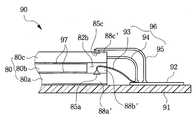
도 7은 본 발명의 제 1 실시예에 따른 인덴트 칩을 이용한 반도체 패키지를 보여주는 사시도이다.7 is a perspective view illustrating a semiconductor package using an indent chip according to a first embodiment of the present invention.
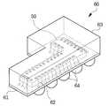
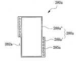
도 8은 본 발명의 제 1 실시예에 따른 인덴트 칩을 포함하는 멀티 칩 패키지를 보여주는 사시도이다.8 is a perspective view illustrating a multi-chip package including an indent chip according to a first embodiment of the present invention.
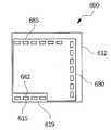
도 9a 내지 도 9d는 본 발명의 제 1 실시예에 따른 인덴트 칩을 포함하는 멀 티 칩 패키지의 다른 예를 보여주는 평면도들이다.9A to 9D are plan views illustrating another example of a multi chip package including an indent chip according to a first embodiment of the present invention.
도 10은 본 발명의 제 2 실시예에 따른 주변회로 영역에 요부가 형성된 인덴트 칩들을 보여주는 평면도이다.FIG. 10 is a plan view illustrating indent chips having recesses formed in a peripheral circuit area according to a second exemplary embodiment of the present invention.
도 11 및 도 12는 본 발명의 제 2 실시예에 따른 인덴트 칩을 갖는 웨이퍼를 스텔스 다이싱 방법으로 개별 인덴트 칩으로 분리한 상태를 보여주는 평면도들이다.11 and 12 are plan views illustrating a state in which a wafer having an indent chip according to a second embodiment of the present invention is separated into individual indent chips by a stealth dicing method.
도 13 및 도 14는 본 발명의 제 2 실시예에 따른 인덴트 칩들이 적층된 멀티 칩 패키지를 보여주는 도면이다.13 and 14 illustrate a multi-chip package in which indent chips are stacked according to a second embodiment of the present invention.
도 15 내지 도 22은 본 발명의 제 2 실시예에 따른 다른 형상의 인덴트 칩들이 적층된 멀티 칩 패키지를 보여주는 평면도들이다.15 to 22 are plan views illustrating multi-chip packages in which indentation chips of different shapes according to the second exemplary embodiment of the present invention are stacked.
도 23 내지 도 25는 본 발명에 따른 서로 다른 형태의 인덴트 칩이 적층된 멀티 칩 패키지를 보여주는 평면도들이다.23 to 25 are plan views illustrating multi-chip packages in which different types of indent chips are stacked according to the present invention.
* 도면의 주요 부분에 대한 설명 *Description of the main parts of the drawing
20, 40 : 웨이퍼 26, 46 : 절단선20, 40: wafer 26, 46: cutting line
30, 50, 80 : 인덴트 칩 31, 51, 81 : 외측면30, 50, 80: indent
32, 52, 82 : 요부 53, 83 : 셀 영역32, 52, 82:
54, 84 : 주변회로 영역 55, 85 : 칩 패드54, 84:
60 : 반도체 패키지 70, 90 : 멀티 칩 패키지60:
88 : 제 1 주변회로 영역 88' : 칩 패드 영역88: first peripheral circuit region 88 ': chip pad region
88" : 인덴트 영역 89 : 제 2 주변회로 영역88 ": indent area 89: second peripheral circuit area
본 발명은 반도체 칩과, 그를 이용한 반도체 패키지 및 멀티 칩 패키지에 관한 것으로, 더욱 상세하게는 외측면에 적어도 하나 이상의 요부를 갖는 인덴트 칩과, 그를 이용한 반도체 패키지 및 멀티 칩 패키지에 관한 것이다.The present invention relates to a semiconductor chip, a semiconductor package and a multi-chip package using the same, and more particularly, to an indent chip having at least one recess on an outer surface thereof, and a semiconductor package and a multi-chip package using the same.
반도체 패키지의 제조 공정은 크게 반도체 웨이퍼 가공(semiconductor wafer fabrication), 패키지 조립(package assembly) 및 테스트(test)로 구분할 수 있다. 웨이퍼 가공 공정은 반도체 물질의 얇고 둥근 판인 웨이퍼의 안 또는 표면에 회로나 소자를 만드는 일련의 조작을 말한다. 이 과정이 끝나면 웨이퍼를 다이싱하여 웨이퍼 상의 반도체 소자를 개별 반도체 칩으로 분리하는 웨이퍼 다이싱(wafer dicing) 공정을 거쳐서, 각각의 개별 반도체 칩을 패키지 상태로 조립하는 패키지 조립 공정을 진행하게 된다.The manufacturing process of the semiconductor package can be largely divided into semiconductor wafer fabrication, package assembly, and test. Wafer processing is a series of operations that create circuits or devices in or on the wafer, which is a thin, rounded plate of semiconductor material. After this process, the wafer is diced, and a wafer dicing process of separating semiconductor devices on the wafer into individual semiconductor chips is performed, and a package assembly process of assembling each individual semiconductor chip into a package is performed.
현재 사용되는 대부분의 반도체 칩(12)은, 도 1에 도시된 바와 같이, 사각 형태를 갖는데 이는 종래의 웨이퍼 다이싱 방법에 기안한다. 종래의 일반적인 웨이퍼 다이싱 공정은 고속으로 회전하는 다이싱 날(18; dicing blade)을 갖는 다이싱 장치(17)를 이용하여 웨이퍼(10) 상에 형성된 다수의 반도체 칩(12) 사이의 절단선(16; scribe line)을 따라 직선 방향으로 다이싱을 수행함으로써 어루어지기 때문에, 웨이퍼(10)에 형성할 수 있는 반도체 칩(12)의 형태를 단순하고 일정한 사각의 형태로만 선택할 수 있었을 뿐, 다양한 형태의 반도체 칩에 대해서는 그 다이 싱이 용이하게 이루어질 수 없었다. 즉, 종래의 웨이퍼 다이싱 방법에서는 원판 형태의 다이싱 날(18)의 물리적 특성을 인해서 직선 경로로만 다이싱을 수행할 수 있었기 때문에, 제조할 수 있는 반도체 칩(12) 또한 사각 형태가 주류를 이루고 있다.Most of the
물론 다이싱 날을 이용하지 않고 레이저를 이용한 레이져 다이싱 방법이 한국공개특허공보 제1998-084225호 및 제1998-067184호에 개시되어 있지만, 이들 모두는 다이싱 날 사용에 따른 문제나 웨이퍼의 손상 방지 등에 대해서만 언급하고 있을 뿐, 사각 형태가 아닌 다른 형태의 반도체 칩을 제조하기 위한 웨이퍼 다이싱 방법에 대해서는 예시하고 있지 못하다. 이것은 현재 출시되고 있는 반도체 칩 형태가 모두 사각 형태를 갖는 것으로부터도 쉽게 짐작할 수도 있다.Of course, laser dicing methods using a laser without using a dicing blade are disclosed in Korean Patent Laid-Open Publication Nos. 1998-084225 and 1998-067184, but all of them are problematic due to the use of a dicing blade or wafer damage. It only mentions prevention and the like, and does not exemplify a wafer dicing method for manufacturing a semiconductor chip having a shape other than a rectangular shape. This can be easily guessed from the fact that all of the semiconductor chip types currently on the market have a rectangular shape.
이와 같은 사각 형태의 반도체 칩을 이용하여 반도체 패키지나 멀티 칩 패키지를 구현할 경우, 예컨대 배선기판에 반도체 칩을 실장하거나, 반도체 칩들을 3차원으로 적층하거나, 동일 평면상에 배치할 수 있는데, 이러한 구성에 있어서 반도체 패키지나 멀티 칩 패키지가 반도체 칩의 형태에 대응되는 획일적인 사각 형태로밖에 제조할 수 없었기 때문에, 기판에의 실장 배치와 공간 활용성에 한계성을 갖는다.When a semiconductor package or a multi-chip package is implemented using such a rectangular semiconductor chip, the semiconductor chip may be mounted on a wiring board, the semiconductor chips may be stacked in three dimensions, or arranged on the same plane. Since the semiconductor package and the multi-chip package can only be manufactured in a uniform rectangular shape corresponding to the shape of the semiconductor chip, there is a limitation in the mounting arrangement and the space utilization on the substrate.
특히 칩 적층 형태의 멀티 칩 패키지를 구현할 때 반도체 칩이 사각 형태를 갖기 때문에, 적층 칩의 두께를 줄이거나 실장 면적을 줄이는데 한계가 있었다. 예를 들어 적층 칩을 구현할 때, 패키지 내에 두 개 이상의 반도체 칩을 적층함에 있어서, 상부에 적층되는 반도체 칩(이하, 적층 칩)이 하부의 반도체 칩(이하, 피 적층 칩)보다 작은 경우에는 문제가 되지 않지만, 반대로 적층 칩이 피적층 칩보다 크기가 동일하거나 유사 혹은 더 클 경우에는 적층 칩과 피적층 칩 사이에 스페이서(spacer)를 개재한다. 스페이서는 피적층 칩에서 인출된 전기적 연결 수단인 본딩 와이어가 적층 칩의 바닥면에 기계적으로 접촉하여 발생될 수 있는 전기적 쇼트를 방지하기 위해서, 본딩 와이어의 루프보다는 높게 형성된다. 그런데 스페이서를 사용하게 되면, 멀티 칩 패키지의 두께가 두꺼워지는 문제가 있다.In particular, since the semiconductor chip has a quadrangular shape when implementing a multi-chip package having a chip stacking type, there is a limit in reducing the thickness of the stacked chip or reducing the mounting area. For example, when implementing a stacked chip, when stacking two or more semiconductor chips in a package, there is a problem when a semiconductor chip (hereinafter referred to as a stacked chip) stacked on the upper side is smaller than a lower semiconductor chip (hereinafter referred to as a stacked chip). On the contrary, when the stacked chips are the same size, similar or larger than the stacked chips, a spacer is interposed between the stacked chips and the stacked chips. The spacers are formed higher than the loops of the bonding wires in order to prevent electrical shorts that can occur due to mechanical bonding of the bonding wires drawn out from the stacked chips by mechanical contact with the bottom surface of the stacked chips. However, when the spacer is used, there is a problem that the thickness of the multi-chip package becomes thick.
이와 같은 문제점을 극복하기 위해서, 일본공개특허공보 제2000-49279호, 한국공개특허공보 제2003-2476호에는, 피적층 칩의 칩 패드에서 인출된 본딩 와이어의 간섭을 방지하기 위해서, 피적층 칩의 칩 패드에 대응되는 상부의 적층 칩의 배면 부분을 깎아서 피적층 칩 위에 적층 칩이 직접 적층된 예가 개시되어 있다. 그런데 적층 칩의 칩 패드는 배면이 깎여진 가장자리 부분의 상부면에 형성되기 때문에, 와이어 본딩 공정 중에 두께가 얇은 적층 칩의 가장자리 부분이 깨지는 불량이 발생될 수 있다.In order to overcome such a problem, Japanese Laid-Open Patent Publication No. 2000-49279 and Korean Laid-Open Patent Publication No. 2003-2476 disclose a stacked chip in order to prevent interference of the bonding wires drawn out from the chip pad of the stacked chip. An example is disclosed in which a laminated chip is directly stacked on a stacked chip by shaving a rear portion of an upper stacked chip corresponding to a chip pad of a chip. However, since the chip pad of the stacked chip is formed on the upper surface of the cut edge portion, a defect in which the edge portion of the thin stacked chip is broken during the wire bonding process may occur.
피적층 칩 위에 직접 적층 칩을 적층하는 다른 방법으로 일본공개특허공보 제2001-196526호에 개시된 바와 같이, 피적층 칩 위에 적층 칩을 비스듬하게 계단식으로 적층할 수도 있는데. 이 경우 적층할 수 있는 반도체 칩 수에 한계가 있으며 적층된 반도체 칩의 실장 면적이 증가하는 문제점을 안고 있다.As another method of laminating the stacked chip directly on the stacked chip, as described in Japanese Patent Laid-Open No. 2001-196526, the stacked chip may be stacked obliquely on the stacked chip. In this case, there is a limit to the number of semiconductor chips that can be stacked, and the mounting area of the stacked semiconductor chips increases.
따라서, 본 발명의 목적은 다양한 형태의 반도체 칩을 제공하여 기판에의 공간활용 효율을 높이는 데 있다.Accordingly, it is an object of the present invention to provide various types of semiconductor chips to increase the space utilization efficiency of the substrate.
본 발명의 다른 목적은 적층되는 반도체 칩의 실장 면적의 증가없이 피적층 칩에 대응되는 크기의 적층 칩을 직접 적층할 수 있도록 하는 데 있다.It is another object of the present invention to directly stack stacked chips having a size corresponding to the stacked chips without increasing the mounting area of the stacked semiconductor chips.
상기 목적을 달성하기 위하여, 본 발명은 스텔스 다이싱 방법으로 웨이퍼를 다이싱하여 얻어진 인덴트 칩으로, 외측면에서 안쪽으로 적어도 하나 이상의 요부를 갖는 인덴트 칩을 제공한다.In order to achieve the above object, the present invention is an indent chip obtained by dicing a wafer by a stealth dicing method, to provide an indent chip having at least one recess in the outer side inward.
즉, 본 발명은 활성면에 다수개의 칩 패드가 형성되고, 외측면에서 안쪽으로 적어도 하나 이상의 요부가 형성된 것을 특징으로 하는 인덴트 칩을 제공한다.That is, the present invention provides an indent chip, characterized in that a plurality of chip pads are formed on the active surface, and at least one recessed portion is formed inward from the outer surface.
바람직한 실시 양태에 따른 인덴트 칩은, 중심 부분의 셀 영역과; 상기 셀 영역을 둘러싸며 칩 패드들이 형성되는 주변회로 영역;을 포함하며, 상기 셀 영역의 외측면에서 안쪽으로 적어도 하나 이상의 요부가 형성된다.An indent chip according to a preferred embodiment comprises: a cell region of a central portion; And a peripheral circuit region surrounding the cell region and in which chip pads are formed, wherein at least one recess is formed inward from an outer surface of the cell region.
본 발명은 전술된 인덴트 칩을 포함하는 반도체 패키지를 제공한다. 즉, 활성면에 다수개의 칩 패드가 형성되고, 외측면에서 안쪽으로 적어도 하나 이상의 요부가 형성된 인덴트 칩과; 상기 인덴트 칩의 형상에 대응되는 배선기판과; 상기 인덴트 칩의 칩 패드와 상기 배선기판을 전기적으로 연결하는 전기적 연결 수단과; 상기 배선기판 위의 인덴트 칩과 전기적 연결 수단을 봉합하는 수지 봉합부; 및 상기 배선기판의 하부면에 형성된 외부접속단자;를 포함하는 것을 특징으로 하는 인덴트 칩을 갖는 반도체 패키지를 제공한다.The present invention provides a semiconductor package including the aforementioned indent chip. That is, an indent chip having a plurality of chip pads formed on the active surface, and at least one recessed portion formed inward from the outer surface; A wiring board corresponding to the shape of the indent chip; Electrical connection means for electrically connecting the chip pad of the indent chip and the wiring board; A resin encapsulation portion for sealing the indent chip and the electrical connection means on the wiring board; And an external connection terminal formed on a lower surface of the wiring board.
본 발명은 또한 전술된 인덴트 칩을 포함하여 다수의 반도체 칩이 평면적으로 실장된 멀티 칩 패키지를 제공한다. 즉, 배선기판에 적어도 하나 이상의 반도 체 칩이 평면적으로 실장된 멀티 칩 패키지로서, 상기 반도체 칩은 활성면에 다수개의 칩 패드가 형성되고, 외측면에서 안쪽으로 적어도 하나 이상의 요부가 형성된 인덴트 칩을 적어도 하나 이상 포함하는 것을 특징으로 하는 멀티 칩 패키지를 제공한다.The present invention also provides a multi-chip package in which a plurality of semiconductor chips are planarly mounted including the aforementioned indent chip. That is, a multi-chip package in which at least one semiconductor chip is planarly mounted on a wiring board, wherein the semiconductor chip has a plurality of chip pads formed on an active surface, and an indented chip having at least one recessed portion inward from an outer surface thereof. It provides a multi-chip package comprising at least one.
본 발명의 바람직한 다른 실시 양태에 따른 인덴트 칩은, 중심 부분의 셀 영역과; 상기 셀 영역을 둘러싸며 칩 패드들이 형성되는 주변회로 영역;을 포함하며, 상기 주변회로 영역에는 외측면에서 안쪽으로 적어도 하나 이상의 요부가 형성된다.Indent chip according to another preferred embodiment of the present invention, the cell region of the central portion; And a peripheral circuit region surrounding the cell region and in which chip pads are formed, wherein the peripheral circuit region has at least one recessed portion formed inward from an outer surface thereof.
그리고 본 발명은 다른 실시 양태에 따른 다수개의 인덴트 칩을 적층한 멀티 칩 패키지를 제공한다. 즉, 배선기판 위에 적층된 다수개의 인덴트 칩을 포함하는 멀티 칩 패키지에 있어서, 상기 인덴트 칩은, 중심 부분의 셀 영역과, 상기 셀 영역을 둘러싸며 칩 패드들이 형성되며, 외측면에서 안쪽으로 적어도 하나 이상의 요부가 형성된 주변회로 영역을 포함하며, 피적층 인덴트 칩의 칩 패드가 노출되게 적층 인덴트 칩에는 요부가 형성된 것을 특징으로 하는 멀티 칩 패키지를 제공한다.The present invention also provides a multi-chip package in which a plurality of indent chips are stacked according to another embodiment. That is, in a multi-chip package including a plurality of indent chips stacked on a wiring board, the indent chip includes a cell region of a central portion and chip pads formed around the cell region, and the inner side of the indent chip. The multi-chip package may include a peripheral circuit region in which at least one recess is formed, and recesses are formed in the stacked indent chip so that the chip pads of the stacked indent chip are exposed.
이하, 첨부 도면을 참조하여 본 발명의 실시예를 보다 상세하게 설명하고자 한다.Hereinafter, with reference to the accompanying drawings will be described in detail an embodiment of the present invention.
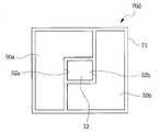
도 2는 본 발명에 따른 요부(32)를 갖는 인덴트 칩(30)을 보여주는 평면도이다. 도 2를 참조하면, 본 발명에 따른 반도체 칩(30)은 외측면(31)에서 안쪽으로 요부(36; indent)가 형성된 구조를 갖는다. 이하 설명에 있어서 본 발명에 따른 반도체 칩(30)을 인덴트 칩(indent chip)이라 하고, 일반적인 사각 형태의 반도체 칩을 노말 칩(normal chip)이라 한다. 즉 종래의 노말 칩은 사각 형태인데 반하여, 본 발명에 따른 인덴트 칩(30)은 외측면(31)에서 안쪽으로 적어도 하나 이상의 요부(36)가 형성됨으로써 다양한 형태로 구현된다.2 is a plan view showing an
구체적으로 설명하면, 인덴트 칩의 외측면(31)은 마주보는 수직 방향의 제 1 외측면(36)과, 제 1 외측면(36)과 이웃하여 서로 마주보는 수평 방향의 제 2 외측면(37)으로 정의되며, 제 1 외측면(36)과 제 2 외측면(37)이 만나는 일측의 모서리에 요부(32)가 형성된 구조를 갖는다. 따라서 인덴트 칩(30)은 영문자 "L"자 형태로 구현할 수 있다.Specifically, the
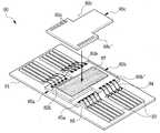
이와 같은 인덴트 칩(30)을 갖는 웨이퍼(20, 40)는 도 3 및 도 4에 도시된 바와 같이 구현이 가능하며, 인덴트 칩(30)을 제조하기 위한 웨이퍼 다이싱 방법으로는 인덴트 칩(30)의 형상에 따른 다이싱 경로를 자유롭게 바꿀 수 있는 레이저 다이싱 방법이 사용되며, 특히 동경정밀(TOKYO SEIMITSU CO.,LTD.)의 레이져 다이싱 장치인 마호 다이싱 장치(Mahoh dicing machine)를 이용한 스텔스 다이싱 방법(stealth dicing method)을 사용하는 것이 바람직하다. 스텔스 다이싱 방법은 웨이퍼에 대해서 투과성 파장의 레이저광의 초점을 웨이퍼(20, 40) 내부에 맞춰 웨이퍼 다이싱을 진행한 다음, 실리콘 소재의 웨이퍼의 결정성을 이용하여 웨이퍼를 지지하는 테이프를 확장시켜 개별 반도체 칩으로 분리하는 방법이다. 스텔스 다이싱 방법은 일반적인 레이저 다이싱 방법과 달리 웨이퍼의 내부만을 선택적으로 개질하고, 웨이퍼 표면에서는 레이저광을 거의 흡수하지 않기 때문에, 웨이퍼 표면이 용융되는 일이 없어 발진이나 열변성층 없이 깨끗하게 다이싱할 수 있는 방법이다. 그 외 웨이퍼의 두께에 상관없이 웨이퍼의 고속 및 정밀한 다이싱이 가능하고, 완전 드라이 프로세스로 세정이 필요 없으며, 비접촉 다이싱 방식으로 정전기가 발생하지 않는 등의 장점이 있다.The
먼저 도 3을 참조하면, 웨이퍼(20)는 개별 인덴트 칩(30)이 독립적으로 격자 배열된 형태로 구현될 수 있다. 이 경우 인덴트 칩(30)을 구분하는 절단선(26)은 수직 방향의 수직 절단선(26a)과 수평 방향의 수평 절단선(26b)이 직선 형태로 형성되고, 그리고 인덴트 칩의 요부(36)에 대응되게 수직 절단선(26a)과 수평 절단선(26b)이 교차하는 일측의 모서리 안쪽에 요부 절단선(26c)이 형성된다. 따라서 웨이퍼(20) 절단은 수평과 수직 절단선(26a, 26b)을 따라서 일차 다이싱을 진행한 다음, 요부 절단선(26c)을 포함할 수 있도록 수직 또는 수평 절단선(26a, 26b)을 따라서 이차 다이싱을 진행한다. 반대로 일차 다이싱과 이차 다이싱의 순서를 바꾸어 진행하여도 무방하다. 아울러 일차 다이싱을 진행한 다음 요부 절단선(26c)만 선별적으로 다이싱을 진행할 수도 있다. 이 또한 요부 절단선(26c)만 먼저 선별적으로 다이싱을 진행한 다음 일차 다이싱을 진행할 수도 있다.First, referring to FIG. 3, the
다음으로 도 4를 참조하면, 웨이퍼(40)는 두 개의 인덴트 칩(30)이 맞물려 사각 형태를 이루는 인덴트 칩 세트(30a)가 격자 배열된 형태로 구현될 수 있다. 웨이퍼(40) 다이싱은 인덴트 칩 세트(30a) 외곽의 수직 및 수평 절단선(46a, 46b)을 따라서 일차 다이싱을 진행한 다음, 수직 방향의 요부 절단선(46c)을 따라서 이차 다이싱을 진행한다. 반대로 일차 다이싱과 이차 다이싱의 순서를 바꾸어 진행 하여도 무방하다. 이때 두 개의 인덴트 칩 세트(30a)로 사각 형태를 이루기 때문에, 도 2의 웨이퍼(20)에 비해서 인덴트 칩(30)을 조밀하게 형성하여 스크랩되는 웨이퍼 부분을 최소화함으로써, 웨이퍼(40)당 제조할 수 있는 인덴트 칩(30)의 수에 이득이 있다.Next, referring to FIG. 4, the
한편 도 2 내지 도 4에 개시된 인덴트 칩(30)은 일측의 모서리에 요부(36)가 형성된 예를 개시하였지만, 도 5에 도시된 바와 같이, 외측면에 적어도 하나 이상의 요부를 형성하여 다양한 형태로 구현할 수 있다. 즉, 도 5의 (a) 내지 (e)에는 제 1 외측면과 제 2 외측면으로 정의된 면에 각기 적어도 하나 이상의 요부가 형성된 인덴트 칩이 개시되어 있고, 도 5의 (f) 내지 (j)에는 제 1 외측면과 제 2 외측면이 만나는 모서리 중 적어도 하나 이상에 요부가 형성된 인덴트 칩이 개시되어 있다. 도 5의 (a) 내지 (j)에서는 인덴트 칩의 제 1 외측면 또는 제 2 외측면에 하나의 요부가 형성된 예를 개시하였지만, 하나 이상의 요부를 제 1 외측면 또는 제 2 외측면에 형성할 수도 있다. 예컨대, 도 5의 (k)에 도시된 바와 같이, 인덴트 칩은 일측의 제 2 외측면에 두 개의 요부가 형성되어 있다.Meanwhile, although the
한편 인덴트 칩은 중심 부분에 집적회로들이 형성되는 셀 영역과, 셀 영역을 둘러싸는 주변회로 영역을 포함하며, 주변회로 영역에 칩 패드들이 형성된다. 이때 요부는, 도 6a 및 도 도6b에 도시된 바와 같이 셀 영역(53)을 침범하여 형성할 수도 있고, 도 10에 도시된 바와 같이 주변회로 영역(84)에만 형성할 수도 있다.An indent chip includes a cell region in which integrated circuits are formed in a central portion and a peripheral circuit region surrounding the cell region, and chip pads are formed in the peripheral circuit region. In this case, the main portion may be formed by invading the
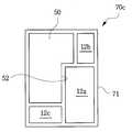
먼저 도 6a는 본 발명의 제 1 실시예에 따른 셀 영역(53)에 요부(52)가 형성된 인덴트 칩(50)을 보여주는 평면도이다. 도 6a를 참조하면, 제 1 실시예에 따른 인덴트 칩(50)은 셀 영역(53)의 외측면(51)에서 안쪽으로 요부(52)가 형성되며, 요부(52)가 형성된 셀 영역의 외측면(51)을 따라서 주변회로 영역(54)이 형성된 구조를 갖는다. 이때 칩 패드(55)는 인덴트 칩(50)의 활성면의 가장자리 영역에 형성된 주변회로 영역(54)을 따라서 형성된다. 즉, 제 1 실시예에 따른 인덴트 칩(50)은 셀 영역(53) 일측의 제 1 외측면(56)과 제 2 외측면(57)이 만나는 가상의 모서리에서 안쪽으로 요부(52)가 형성되며, 요부(52)를 갖는 셀 영역의 외측면(51)을 따라서 주변회로 영역(54)이 형성되어 있다.6A is a plan view illustrating an
한편 칩 패드(55)는 요부(52)가 형성된 주변회로 영역(54a)에 형성되어 있지만, 도 6b에 도시된 바와 같이 요부(52)가 형성된 주변회로 영역(54a)에 칩 패드가 형성되지 않을 수도 있다.Meanwhile, although the
제 1 실시예에 따른 인덴트 칩(50)을 이용한 반도체 패키지(60)의 일 예가 도 7에 도시되어 있다. 도 7을 참조하면, 반도체 패키지(60)는 "L"자형의 인덴트 칩(50)을 포함할 수 있는 "L"자형의 배선기판(61) 위에 인덴트 칩(50)이 실장된 구조를 갖는다. 인덴트 칩(50)과 배선기판(61)은 본딩 와이어(62)에 의해 전기적으로 연결되며, 배선기판(61) 상부면에 형성된 인덴트 칩(50)과 본딩 와이어(62)는 수지 봉합부(63)에 의해 보호된다. 그리고 배선기판(61)의 하부면에 인덴트 칩(50)과 전기적으로 연결된 외부접속단자(64)가 형성된 구조를 갖는다. 외부접속단자로(64)로 주로 솔더 볼이 사용된다.An example of the
즉, 제 1 실시예에 따른 인덴트 칩(50)을 갖는 반도체 패키지(60)는 종래의 획일적인 사각 타입의 반도체 패키지 형태에서 벗어나 인덴트 칩(50)의 형상에 대 응되는 "L"자형의 반도체 패키지(60)로 구현할 수 있다. 즉, 반도체 패키지(60)는 내장되는 인덴트 칩(50)의 형상에 따라서 다양한 형태로 구현할 수 있기 때문에, 반도체 패키지(60)가 실장되는 기판의 공간활용의 효율을 높일 수 있다. 아울러 기판 내의 반도체 패키지들의 실장 밀도를 높일 수 있기 때문에, 기판 크기를 줄일 수 있는 장점도 있다.That is, the
한편 본 발명의 실시예에서는 인덴트 칩(50)과 배선기판(60)의 전기적 연결 방법으로 와이어 본딩법을 개시하였지만, 플립 칩 본딩법 또는 탭 본딩법을 사용할 수도 있다. 배선기판(60)으로는 리드 프레임, 인쇄회로기판, 테이프 배선기판, 세라믹 기판 등이 사용될 수 있다.Meanwhile, in the exemplary embodiment of the present invention, the wire bonding method is disclosed as an electrical connection method between the
제 1 실시예에 따른 인덴트 칩(50)을 포함하는 멀티 칩 패키지(70)의 일 예가 도 8에 도시되어 있다. 도 8을 참조하면, 멀티 칩 패키지(70)는 "L"자형의 인덴트 칩(50)의 형상에 대응되는 "L"자형의 배선기판(71)에 인덴트 칩(50)이 실장되고, 인덴트 칩(50)의 일측에 노말 칩(12)이 실장된 구조를 갖는다. 즉, 획일적인 사각 타입의 종래의 멀티 칩 패키지 형태를 본 발명에 개시된 바와 같이 "L"자형의 멀티 칩 패키지(70)로 구현할 수도 있다.An example of the
그 외 제 1 실시예에 따른 인덴트 칩(50, 50a, 50b)을 이용하여, 도 9a 내지 도 9c에 개시된 바와 같이, 다양한 배치 구조의 멀티 칩 패키지(70a, 70b, 70c, 70d)를 구현할 수 있다. 한편 도 9c 및 도 9d에서는 인덴트 칩(50)과 노말 칩(12, 12a, 12b, 12c)의 배치에 주목하여 멀티 칩 패키지(70c, 70d)의 구조를 단순하게 나타내었다. 그리고 도 9bb는 도 9b의 9b'-9b'선 단면도이다.In addition, using the indentation chips 50, 50a, and 50b according to the first embodiment, as shown in FIGS. 9A to 9C,
도 9a를 참조하면, 멀티 칩 패키지(70a)는 배선기판(71) 위에 인덴트 칩(50)과 노말 칩(12)이 평면적으로 배치되는데, 인덴트 칩의 요부(52)와 이웃하게 노말 칩(12)이 배치된 구조를 갖는다. 인덴트 칩(50)과 노말 칩(12)은 본딩 와이어(73)에 의해 배선기판의 기판 패드(72)에 전기적으로 연결된다. 이때 인덴트 칩의 요부(52)와 이웃하는 노말 칩(12)의 일측에 형성된 칩 패드(15)와 인덴트 칩의 요부(52) 영역에 노출된 배선기판(71) 부분에 형성된 기판 패드(72a)가 본딩 와이어(73a)에 의해 전기적으로 연결된 구조를 갖는다. 즉, 인덴트 칩의 요부(52) 영역에 노출된 배선기판(12) 부분이 기판 패드(72a)를 형성할 수 있는 영역으로 사용되었다.Referring to FIG. 9A, in the
한편 인덴트 칩의 요부 영역은, 도 9b 내지 도 9d에 도시된 바와 같이, 인덴트 칩 또는 노말 칩이 배치될 수 있는 영역으로 사용될 수도 있다. 즉, 도 9b 및 도 9bb를 참조하면, 멀티 칩 패키지(70b)는 배선기판(71) 위에 인덴트 칩(50)과 노말 칩(12)이 평면적으로 배치되는데, 인덴트 칩의 요부(52) 안에 노말 칩(12)이 배치된 구조를 갖는다. 이때 인덴트 칩(50)은 배선기판(71)과 본딩 와이어(73)에 의해 전기적으로 연결되고, 노말 칩(12)은 배선기판(71)에 플립 칩 본딩된다.Meanwhile, the main region of the indent chip may be used as an area where the indent chip or the normal chip may be disposed, as shown in FIGS. 9B to 9D. That is, referring to FIGS. 9B and 9BB, in the
도 9c를 참조하면, 멀티 칩 패키지(70c)는 인덴트 칩의 요부(52)에 다른 노말 칩(12b, 12c)에 비해서 상대적으로 큰 제 1 노말 칩(12a)의 일측이 배치되고, 인덴트 칩(50)과 제 1 노말 칩(12a) 사이의 공간에 두 개 노말 칩(12b, 12c)이 배치되어 전체적으로는 사각 형태를 이룬다.Referring to FIG. 9C, in the
그리고 도 9d를 참조하면, 멀티 칩 패키지(70d)는 두 개의 인덴트 칩(50a, 50b)의 요부(52a, 52b)가 사각 링을 이루도록 배치되고, 두 개의 인덴트 칩(50a, 50b) 사이의 요부(52a, 52b)가 형성하는 공간에 노말 칩(12)이 배치된 구조를 갖는다.Referring to FIG. 9D, the
따라서 평면적인 멀티 칩 패키지의 반도체 칩 배치에 있어서 인덴트 칩을 사용함으로써, 배선기판의 공간활용의 효율을 높일 수 있다. 예컨대, 인덴트 칩의 요부에 노출된 배선기판 부분에 기판 패드를 형성할 수도 있고, 다른 반도체 칩들이 실장될 수 있는 영역으로 사용할 수 있다. 아울러 배선기판 내의 반도체 칩들의 실장 밀도를 높일 수 있기 때문에, 멀티 칩 패키지 크기를 줄일 수 있는 장점도 있다.Therefore, the use of indent chips in the planar semiconductor chip arrangement of the multi-chip package can increase the efficiency of space utilization of the wiring board. For example, the substrate pad may be formed in a portion of the wiring board exposed to the main portion of the indent chip, or may be used as an area in which other semiconductor chips may be mounted. In addition, since the mounting density of the semiconductor chips in the wiring board can be increased, the size of the multi-chip package can be reduced.
한편, 제 1 실시예에 따른 "L"자형의 인덴트 칩을 갖는 반도체 패키지 및 멀티 칩 패키지는 일 예에 불과하며, 도 5에 개시된 바와 같은 다양한 형태의 인덴트 칩을 이용하여 다양한 형태의 반도체 패키지 및 멀티 칩 패키지를 구현할 수 있음은 물론이다.Meanwhile, the semiconductor package and the multi-chip package having the “L” shaped indentation chip according to the first embodiment are just examples, and various types of semiconductors may be used by using various types of indentation chips as shown in FIG. 5. Of course, packages and multi-chip packages can be implemented.
도 10은 본 발명의 제 2 실시예에 따른 주변회로 영역(84)에 요부(82)가 형성된 인덴트 칩(80)을 보여주는 평면도이다. 도 10을 참조하면, 제 2 실시예에 따른 인덴트 칩(80)은 중심 부분의 셀 영역(83)과, 셀 영역(83)을 둘러싸며 칩 패드들(85)이 형성되는 주변회로 영역(84)을 포함하며, 주변회로 영역(84)에는 외측면(81)에서 안쪽으로 적어도 하나 이상의 요부(82)가 형성된 구조를 갖는다.FIG. 10 is a plan view illustrating an
좀 더 구체적으로 설명하면, 주변회로 영역(84)은 마주보는 제 1 외측면(86)에 대응되는 위치의 제 1 주변회로 영역(88)과, 제 1 주변회로 영역(88)에 이웃하 며 마주보는 제 2 외측면(87)에 대응되는 제 2 주변회로 영역(89)을 포함한다. 이때 칩 패드(85)는 인덴트 칩(80)의 활성면 양쪽의 가장자리 영역에 형성된 제 1 주변회로 영역(88)을 따라서 형성된다. 제 1 주변회로 영역(88)은 칩 패드(85)가 형성된 칩 패드 영역(88')과, 요부(82)가 형성되는 인덴트 영역(88")을 포함한다.More specifically, the
제 2 실시예에 따른 인덴트 칩(80)은 인덴트 칩(80)을 3차원으로 적층하여 멀티 칩 패키지로 구현 시, 적층되는 인덴트 칩의 실장 면적의 증가없이 인덴트 칩의 두께의 합에 대응되는 두께로 적층할 수 있는 소스를 제공한다. 인덴트 칩들을 3차원으로 적층할 때, 피적층 인덴트 칩의 칩 패드가 적층 인덴트 칩의 요부로 노출될 수 있도록, 인덴트 영역(88")에 칩 패드 영역(88')보다는 적어도 크게 요부(82)를 형성하는 것이 바람직하다. 제 2 실시예에서는 칩 패드 영역(88')과 요부(82)가 거의 동일한 크기로 형성된 예를 개시하고 있다.The
한편 제 2 실시예에 따른 인덴트 칩(80)을 갖는 웨이퍼는 도 11 및 도 12에 도시된 바와 같이 구현이 가능하며, 인덴트 칩(80)을 제조하기 위한 웨이퍼 다이싱 방법으로 스텔스 다이싱 방법이 사용된다.Meanwhile, the wafer having the
도 11을 참조하면, 웨이퍼는 개별 인덴트 칩(80)이 독립적으로 격자 배열된 형태로 구현된다. 바람직하게는 이웃하는 인덴트 칩의 칩 패드 영역(88')과 인덴트 영역(88")이 서로 마주보게 배치된 구조로 구현하는 것이다.Referring to FIG. 11, the wafer is implemented in a form in which individual indentation chips 80 are independently arranged in a lattice arrangement. Preferably, the
도 12를 참조하면, 웨이퍼는 인덴트 칩의 요부(82)에 인접한 인덴트 칩의 칩 패드 영역(88')이 배치되어 서로 맞물린 형태로 구현할 수 있다. 이 경우 인덴트 칩의 칩 패드 영역(88')과 요부(82)가 거의 동일한 크기로 구현된다.Referring to FIG. 12, the wafer may be implemented in a form in which
도 13 및 도 14는 본 발명의 제 2 실시예에 따른 인덴트 칩들(80)이 적층된 멀티 칩 패키지(90)를 보여주는 도면이다. 도 13 및 도 14를 참조하면, 멀티 칩 패키지(90)는 배선기판(91) 위에 제 2 실시예에 따른 인덴트 칩(80) 3개가 3차원으로 적층된 구조를 갖는다. 이때 피적층 인덴트 칩(80a, 80b)의 칩 패드들(85a, 85b)이 적층 인덴트 칩(80b, 80c)의 요부(82b, 82c)를 통하여 노출될 수 있도록 칩 적층이 이루어진다. 적층 인덴트 칩의 요부(82b, 82c)로 노출된 피적층 인덴트 칩의 칩 패드(85a, 85b)와 배선기판(91)은 본딩 와이어(96)에 의해 전기적으로 연결된다. 즉, 피적층 인덴트 칩(80a, 80b)이 적층된 방향에 대해서 적층 인덴트 칩(80b, 80c)은 180도 회전된 방향으로 적층된다. 따라서, 인덴트 칩 위에 스페이서의 개재 없이 크기가 동일한 인덴트 칩을 직접 적층할 수 있다. 한편 이하의 설명에 있어서, 배선기판(91) 위에 적층되는 인덴트 칩(80)의 순서에 따라서 제 1 칩(80a), 제 2 칩(80b), 제 3 칩(80c)이라 하며, 본 실시예에서는 동일한 인덴트 칩(80) 3개가 적층된 예를 개시하였다. 적층 인덴트 칩과 피적층 인덴트 칩은 상대적인 것으로, 제 1 칩(80a)이 피적층 인덴트 칩인 경우 제 2 칩(80b)이 적층 인덴트 칩이 되고, 제 2 칩(80b)이 피적층 인덴트 칩인 경우 제 3 칩(80c)이 적층 인덴트 칩이 된다.13 and 14 illustrate a
좀 더 구체적으로 설명하면, 배선기판(91) 위에 제 1 칩(80a)이 실장된다. 제 1 칩(80a)으로는 제 2 실시예에 따른 인덴트 칩이 사용된 예를 개시하였지만, 제 2 실시예에 따른 인덴트 칩과 칩 패드 배열이 동일한 노말 칩이 사용될 수 있다. 배선기판(91)의 상부면에는 제 1 칩의 제 1 외측면(86)을 향하여 근접하게 기 판 패드들(92)이 뻗어 있다.In more detail, the
제 2 칩(80b)이 제 1 칩(80a) 위에 비전도성 접착제(97)를 개재하여 적층된다. 이때 제 1 칩의 제 1 칩 패드들(85a)이 제 2 칩의 제 2 요부(82b)에 노출될 수 있도록 적층된다. 즉, 제 1 칩(80a)이 실장된 방향에 대해서 180도 회전된 방향으로 제 2 칩(80b)이 제 1 칩(80a) 위에 적층된다. 이때 제 1 칩 패드들(85a)이 제 2 요부(82b)를 통하여 외부로 노출될 수 있도록 제 1 칩 패드 영역(88a')보다는 동일하거나 크게 제 2 요부(82b)를 형성하는 것이 바람직하다. 비전도성 접착제(97)로는 비전도성의 액상이나 얇은 필름이나 테이프 형상의 접착제가 사용될 수 있다.The
제 3 칩(80c)이 제 2 칩(80b) 위에 비전도성 접착제(97)를 개재하여 적층된다. 제 3 칩(80c)은 제 2 칩 패드들(85b)이 제 3 요부(82c)에 노출되게 적층될 수 있도록, 제 1 칩(80a)과 동일 방향으로 적층된다. 이때 제 1 칩(80a)과 제 3 칩(80c)은 동일 방향으로 적층되기 때문에, 제 2 칩(80b)을 사이에 두고 제 3 칩 패드 영역(88c')에 의해 제 1 칩의 칩 패드 영역(88a')이 가려진다.The
따라서 제 2 실시예에 따른 인덴트 칩(80)을 사용하여 칩 적층을 구현함으로써, 종래의 동일 칩 적층시 필요했던 스페이서의 개재 없이 3차원으로 칩 적층이 가능하다. 아울러 인덴트 칩(80)의 실장 면적의 증가없이 적층되는 인덴트 칩(80)들의 두께의 합에 대응되는 두께로 적층이 가능하다. 이때 종래의 스페이서의 역할은 피적층 인덴트 칩 위에 적층되는 적층 인덴트 칩이 대신하게 된다. 물론, 본 실시예에서는 3개의 인덴트 칩(80)이 적층된 예를 개시하였지만, 더 많은 수의 인 덴트 칩을 적층할 수도 있다.Therefore, by implementing the chip stack using the
그리고 제 1 내지 제 3 칩 패드(85a, 82b, 82c)와 배선기판의 기판 패드(92)는 본딩 와이어(96)에 의해 전기적으로 연결된다. 본딩 와이어(96)는 필요에 따라서 볼 본딩법, 리버스 본딩법 또는 범프 리버스 본딩법으로 형성할 수 있다. 본 실시예에서는 제 1 칩(80a)과 배선기판(91)은 볼 본딩법으로 형성된 제 1 와이어(93)에 의해 전기적으로 연결되며, 제 2 칩(80b) 및 제 3 칩(80c)은 범프 리버스 본딩법으로 형성된 제 2 및 제 3 와이어(94, 95)에 의해 전기적으로 연결된다. 범프 리버스 본딩법은 와이어 본딩의 접합 신뢰성을 유지하면서 와이어 루프를 최대한 낮게 형성할 수 있는 와이어 본딩 방법 중의 하나이다.The first to
한편 제 1 칩 패드 영역(88a')이 제 3 칩 패드 영역(88c')에 의해 가려지기 때문에, 제 1 칩 패드(85a)에서 인출된 제 1 와이어(93)는 제 3 칩 패드 영역(88c')의 배면보다는 아래쪽에 형성해야 한다. 제 1 칩(80a)을 제외한 제 1 칩(80a) 위에 적층되는 제 2 및 제 3 칩(80b, 80c)의 와이어 본딩법으로는 본딩 와이어(94, 95)의 루프 높이를 최소화할 수 있는 범프 리버스 본딩법을 사용하였다. 이때 제 1 칩(80a)의 와이어 본딩법으로 볼 본딩법을 사용한 이유는, 제 1 칩(80a)의 경우는 배선기판(91) 위에 바로 적층되기 때문에, 볼 본딩으로 제 1 와이어(93)를 형성하더라도 제 3 칩 패드 영역(88c')의 배면보다는 낮게 제 1 와이어(93)를 형성할 수 있기 때문이다. 하지만 제 2 칩(80b)의 두께가 볼 본딩으로 형성되는 제 1 와이어(93)의 루프의 높이보다 낮다면, 제 1 와이어(93)가 제 3 칩 패드 영역(88c')의 배면에 접촉할 수 있기 때문에, 제 1 와이어(93) 또한 범프 리버스 본딩법으로 형성하는 것이 바람직하다. 즉, 제 1 내지 제 3 와이어를 형성하는 방법은 적층되는 인덴트 칩의 두께에 따라서 적절하게 선택하여 사용할 수 있다.On the other hand, since the first
그리고 제 1 내지 제 3 와이어(93, 94, 95) 본딩 공정은 아래의 3가지 방법으로 진행할 수 있다. 첫째 제 1 내지 제 3 칩(80a, 80b, 80c) 적층 공정과 연계하여 차례로 제 1 내지 제 3 와이어(93, 94, 95) 본딩 공정을 차례로 진행하는 방법이다. 둘째 제 1 및 제 2 칩(80a, 80b)을 적층한 다음 제 1 및 제 2 와이어(93, 94) 본딩 공정을 함께 진행하고, 제 3 칩(80c)을 적층한 다음 제 3 와이어(95) 본딩 공정을 진행하는 방법이다. 마지막으로 제 1 칩(80a)을 적층한 다음 제 1 와이어(93) 본딩 공정을 진행하고, 제 2 및 제 3 칩(80b, 80c)을 적층한 다음 제 2 및 제 3 와이어(94, 95) 본딩 공정을 함께 진행하는 방법이다.The bonding process of the first to
한편 제 1 내지 3 칩(80a, 80b, 80c)은 동일 형태의 인덴트 칩으로, 기능 또한 동일한 동일 칩일 수도 있고 기능이 상이한 이종 칩일 수도 있다. 예컨대, 제 1 내지 3 칩(80a, 80b, 80c)이 모두 동일 칩인 경우, 도시되지는 않았지만 동일한 역할을 하는 칩 패드들끼리 서로 연결될 수 있도록, 동일한 역할을 하는 칩 패드들이 본딩되는 기판 패드들을 서로 연결하는 회로 배선이 배선기판(91)에 형성된다. 즉, 제 1 및 제 3 칩(80a, 80c)은 동일 칩 패드(85a, 85c)가 동일 기판 패드(92)에 직접 연결되지만, 제 2 칩(80b)의 경우는 그렇지 못하다. 따라서 제 1 칩(80a)과 연결된 기판 패드(92)와 서로 대응되는 제 2 칩(80b)이 연결된 기판 패드(92)를 서로 연결하는 회로 배선을 배선기판(91)에 형성할 수 있다.Meanwhile, the first to
따라서 인덴트 칩 적층시, 피적층 인덴트 칩의 칩 패드들이 적층 인덴트 칩 의 요부에 노출되게 인덴트 칩을 적층함으로써, 적층되는 인덴트 칩의 실장 면적의 증가없이 실질적으로 인덴트 칩 두께로 적층할 수 있다. 물론 칩 패드가 형성되는 주변회로 영역에 요부를 형성함으로써 칩 패드 영역이 축소되지만, 필요에 따라서 칩 패드 영역에 칩 패드를 2렬 이상으로 형성함으로써 필요한 수의 칩 패드를 축소된 칩 패드 영역 안에 형성할 수 있다.Therefore, in stacking the indent chip, the indent chip is laminated so that the chip pads of the stacked indent chip are exposed to the recessed portion of the stacked indent chip, thereby substantially increasing the indent chip thickness without increasing the mounting area of the stacked indent chip. It can be laminated. Of course, the chip pad region is reduced by forming recesses in the peripheral circuit region where the chip pad is formed. However, if necessary, two or more rows of chip pads are formed in the chip pad region to form the required number of chip pads in the reduced chip pad region. can do.
전술된 멀티 칩 패키지(90)는 마주보는 제 1 주변회로 영역에 요부가 형성된 인덴트 칩이 적층된 예를 개시하였지만, 도 5에 개시된 바와 같이, 제 2 실시예에 따른 인덴트 칩 또한 다양한 형태로 구현이 가능하며 또한 그를 이용한 적층 타입의 멀티 칩 패키지로의 구현도 가능하다. 즉, 도 15 내지 도 22은 본 발명의 제 2 실시예에 따른 다른 형상의 인덴트 칩들이 적층된 멀티 칩 패키지의 다른 예를 보여주는 평면도들이다. 한편 적층시 교대로 동일한 인덴트 칩의 적층이 이루어지기 때문에, 설명의 편의상 2개의 인덴트 칩이 적층된 예를 개시하였다. 물론 2개 이상의 인덴트 칩을 적층하여 멀티 칩 패키지를 구현할 수 있다. 그리고 인덴트 칩의 적층 구조에 주목하여 멀티 칩 패키지 구조를 단순하게 나타내었다.Although the above-described
도 15 및 도 16를 참조하면, 제 2-1 실시예에 따른 인덴트 칩(180a, 180b)은 일측의 주변회로 영역(188a, 188b)에 칩 패드(185a, 185b)와 요부(182a, 182b)가 형성된 구조를 갖는다. 즉, 도 15을 참조하면, 제 1 칩(180a)은 일측의 제 1 주변회로 영역(188a)의 위쪽에 제 1 칩 패드들(185a)이 형성되는 제 1 칩 패드 영역(188a')이, 제 1 칩 패드 영역(188a') 아래쪽에 제 1 요부(182a)가 형성되는 제 1 인덴트 영역(188a")가 형성된 구조를 갖는다. 그리고 도 16를 참조하면, 제 1 칩(180a) 위에 적층되는 제 2 칩(180b)은 일측의 제 1 주변회로 영역(188b)의 위쪽에 제 1 칩 패드 영역(188a')이 노출되게 제 2 요부(182b)가 제 2 인덴트 영역(188b")에 형성되고, 제 2 요부(182b) 아래쪽에 제 2 칩 패드 영역(188b')이 형성된 구조를 갖는다. 한편 칩 적층시 제 2 요부(182b)를 통하여 제 1 칩 패드 영역(188a')이 노출될 수 있도록, 제 2 요부(182b)는 제 1 칩 패드 영역(188a')보다는 적어도 크게 형성하는 것이 바람직하다. 제 1 칩(180a)과 제 2 칩(180b)은 미러(mirror) 칩 형태로 형성된다.15 and 16,
따라서 제 2-1 실시예에 따른 인덴트 칩(180a, 180b)이 적층된 멀티 칩 패키지(190)는 제 2 칩의 제 2 요부(182b)를 제 1 칩의 제 1 칩 패드들(185a)이 외부로 노출됨으로써, 제 1 및 제 2 칩 패드들(185a, 185b) 모두가 외부로 노출된 구조를 갖는다.Accordingly, in the
도 17 및 도 18을 참조하면, 제 2-2 실시예에 따른 인덴트 칩(280a, 280b)은 마주보는 일측의 주변회로 영역(288a, 288b)에 각기 칩 패드 영역(288a', 288b')과 인덴트 영역(288a", 288b")이 형성되며, 마주보는 일측의 주변회로 영역(288a, 288b)에서 칩 패드 영역(288a', 288b')과 인덴트 영역(288a", 288b")이 서로 마주보게 형성되어 있다. 즉, 도 17을 참조하면, 제 1 칩(280a)은 마주보는 제 1 주변회로 영역(288a)에 각기 제 1 칩 패드 영역(288a')과 제 1 요부(282a)를 갖는 제 1 인덴트 영역(288a")이 형성되며, 마주보는 제 1 주변회로 영역(288a)에서 제 1 칩 패드 영역(288a')과 제 1 요부(282a)는 서로 마주보게 형성되어 있다. 그리고 도 18를 참조하면, 제 1 칩(280a) 위에 적층되는 제 2 칩(280b)은 제 1 칩(280a)과는 반대로 제 1 칩 패드 영역(288a')에 대응되는 위치에 제 2 요부(282b)를 갖는 제 2 인덴트 영역(288b")이 형성되고, 제 1 요부(282a)에 대응되게 제 2 칩 패드 영역(288b')이 형성된 구조를 갖는다. 즉, 제 1 칩(280a)과 제 2 칩(280b)은 미러 칩 형태로 형성된다.Referring to FIGS. 17 and 18,
따라서 제 2-2 실시예에 따른 인덴트 칩(280a, 280b)이 적층된 멀티 칩 패키지(290)는 제 2 칩의 제 2 요부(282b)를 제 1 칩의 제 1 칩 패드들(285a)이 외부로 노출됨으로써, 제 1 및 제 2 칩 패드들(285a, 285b) 모두가 외부로 노출된 구조를 갖는다.Accordingly, in the
도 19 및 도 20을 참조하면, 제 2-3 실시예에 따른 인덴트 칩(380a, 380b)은 일측의 대각선 방향의 모서리에 칩 패드 영역(388a', 388b')이 형성되고, 타측의 대각선 방향의 모서리에 요부(382a, 382b)를 갖는 인덴트 영역(388a", 388b")이 형성된 구조를 갖는다. 즉, 제 1 칩(380a)은 오른쪽 상단 모서리와 왼쪽 하단의 모서리에 제 1 칩 패드 영역(388a)'이 형성되고, 왼쪽 상단 모서리와 왼쪽 상단의 모서리에 제 1 요부(382a)가 형성된 구조를 갖는다. 그리고 제 1 칩(382a) 위에 적층되는 제 2 칩(382b)은 제 1 칩(382a)과 반대로 제 1 칩 패드 영역(388a')에 대응되는 대각선 방향의 모서리에 제 2 요부(382b)가 형성되고, 제 1 요부(382a)에 대응되는 위치에 제 2 칩 패드 영역(388b')이 형성된 구조를 갖는다. 즉, 제 1 칩(380a)과 제 2 칩(380b)은 형상이 서로 미러 칩 형태로 형성된다.19 and 20,
따라서 제 2-3 실시예에 따른 인덴트 칩(380a, 380b)이 적층된 멀티 칩 패키지(390)는 제 2 칩의 제 2 요부(382b)를 제 1 칩의 제 1 칩 패드들(285a)이 외부로 노출됨으로써, 제 1 및 제 2 칩 패드들(385a, 385b) 모두가 외부로 노출된 구조를 갖는다.Accordingly, in the
한편 제 1 칩과 제 2 칩은 동일 형상의 칩이어도 무방하다. 즉, 제 2 칩을 제 1 칩(380)에 대해서 일방향으로 90도 또는 270도 회전시켜 적층할 경우, 전술된 적층 구조와 동일한 구조로 적층이 가능하다.On the other hand, the first chip and the second chip may be chips of the same shape. That is, when the second chip is stacked by rotating 90 degrees or 270 degrees in one direction with respect to the first chip 380, the second chip may be stacked in the same structure as the above-described stacking structure.
그리고 도 21 및 도 22를 참조하면, 제 1 칩(480a)은 양측의 대각선 방향의 모서리에 제 1 칩 패드 영역(488a')이 형성되고, 마주보는 제 1 및 제 2 주변회로 영역(488a, 489a)에 제 1 요부(482a)가 형성된 구조를 갖는다. 그리고 제 1 칩(480a) 위에 적층되는 제 2 칩(480b)은 제 1 칩(480a)과는 반대로 양측의 대각선 방향의 모서리에 제 1 칩 패드 영역(488a')이 노출될 수 있는 제 2 요부(482b)가 형성되고, 제 1 요부(482a)에 대응되는 위치에 제 2 칩 패드 영역(488b')이 형성된 구조를 갖는다.21 and 22, in the
따라서 제 2-4 실시예에 따른 인덴트 칩(480a, 480b)이 적층된 멀티 칩 패키지(490)는 제 2 칩의 제 2 요부(482b)를 제 1 칩의 제 1 칩 패드들(485a)이 외부로 노출됨으로써, 제 1 및 제 2 칩 패드들(485a, 485b) 모두가 외부로 노출된 구조를 갖는다.Accordingly, in the
정리하면 인덴트 칩 적층은, 홀수층에 위치하는 인덴트 칩과 짝수층에 위치하는 인덴트 칩들끼리는 동일 방향으로 적층되며, 홀수층 인덴트 칩의 칩 패드 영역이 짝수층 인덴트 칩의 요부에 노출되고, 짝수층 인덴트 칩의 칩 패드 영역이 홀수층 인덴트 칩의 요부에 노출될 수 있도록 적층이 이루어진다.In summary, indentation chip stacking includes indentation chips in odd-numbered layers and indentation chips in even-numbered layers stacked in the same direction, and chip pad regions of the odd-numbered indentation chips are formed in the main portion of the even-numbered indentation chips. The stack is exposed so that the chip pad region of the even layer indent chip is exposed to the recessed portion of the odd layer indent chip.
지금까지는 동일 형태의 제 2 실시예에 따른 인데트 칩이 적층된 멀티 칩 패키지를 개시하였지만, 도 23 내지 도 25에 도시된 바와 같이, 노말 칩과 서로 다른 형태의 인덴트 칩을 적층하여 멀티 칩 패키지를 구현할 수 있다. 물론, 피적층 칩의 칩 패드들이 적층 인덴트 칩의 요부에 노출되게 칩 적층이 이루어진다. 반도체 칩의 적층 구조에 주목하여 멀티 칩 패키지 구조를 단순하게 나타내었다.Until now, a multi-chip package in which an ind chip is stacked according to a second embodiment of the same type has been disclosed, but as shown in FIGS. 23 to 25, a normal chip and a different type of indent chip are stacked to multi-chip. You can implement a package. Of course, chip stacking is performed such that the chip pads of the stacked chip are exposed to the recessed portions of the stacked indent chip. The multi-chip package structure is shown simply by paying attention to the stacked structure of the semiconductor chip.
도 23을 참조하면, 멀티 칩 패키지(590)는 3개의 서로 다른 형태의 반도체 칩(512, 580a, 580b)이 적층된 멀티 칩 패키지로서, 제 1 칩(512)은 양측의 제 1 주변회로 영역(518)에 제 1 칩 패드들(512)이 형성된 노말 칩이다. 제 1 칩(512) 위에 적층되는 제 2 칩(580a)은 제 1 칩의 제 1 칩 패드들(512)이 노출되게 제 1 요부(582a)가 형성된 인덴트 칩으로, 일측의 제 1 주변회로 영역(588a)에 제 2 칩 패드들(585a)이 형성되어 있다. 그리고 제 3 칩(580b)은 제 2 칩의 제 2 칩 패드들(585a)에 이격되게 제 2 칩(580a) 영역 안에 적층되며, 가장자리 둘레에 제 3 칩 패드들(585b)이 형성되어 있다. 제 3 칩(580b)은 제 1 요부(582a)에 대응되는 일측에 제 2 요부(582b)가 형성되어 있다.Referring to FIG. 23, the
도 24를 참조하면, 멀티 칩 패키지(690)는 2개의 서로 다른 형태의 반도체 칩(612, 680)이 적층된 멀티 칩 패키지로서, 제 1 칩(612)은 일측의 제 2 주변회로 영역(619)에 제 1 칩 패드들(615)이 형성된 노말 칩이다. 그리고 제 1 칩(612) 위에 적층되는 제 2 칩(680)은 제 1 칩의 제 1 칩 패드들(615)이 노출되게 요부(682)가 형성된 인덴트 칩으로, 가장자리 둘레에 제 2 칩 패드(685)가 형성되어 있다.Referring to FIG. 24, the
그리고 도 25를 참조하면, 멀티 칩 패키지(790)는 2개의 서로 다른 형태의 반도체 칩(712, 782)이 적층된 멀티 칩 패키지로서, 제 1 칩(712)은 마주보는 양측의 제 1 주변회로 영역(718a, 718b)에 제 1 칩 패드들(715a, 715b)이 형성되어 있다. 이때 제 1 칩 패드들(715a, 715b)은 일측의 제 1 주변회로 영역(718a)을 따라서 균일하게 형성된 제 1-1 칩 패드(715a)와, 타측의 제 1 주변회로 영역(718b)의 중심 부분에 형성된 제 1-2 칩 패드(715b)를 포함한다. 그리고 제 1 칩(712) 위에 적층되는 제 2 칩(780)은 제 1-2 칩 패드들(715b)이 노출되게 요부(782)가 형성된 인덴트 칩이다. 물론 제 2 칩(780)은 제 1-1 칩 패드들(615a)에 이격되게 제 1 칩(712) 영역 안에 적층된다.Referring to FIG. 25, the
그 외 다양한 형태의 인덴트 칩을 이용하여 다양한 형태의 칩 적층을 구현할 수 있음은 물론이다.In addition, various types of chip stacks may be implemented using various types of indent chips.
한편, 본 명세서와 도면에 개시된 본 발명의 실시예들은 이해를 돕기 위해 특정 예를 제시한 것에 지나지 않으며, 본 발명의 범위를 한정하고자 하는 것은 아니다. 여기에 개시된 실시예들 이외에도 본 발명의 기술적 사상에 바탕을 둔 다른 변형예들이 실시 가능하다는 것은, 본 발명이 속하는 기술분야에서 통상의 지식을 가진 자에게 자명한 것이다.On the other hand, the embodiments of the present invention disclosed in the specification and drawings are merely presented specific examples to aid understanding, and are not intended to limit the scope of the present invention. In addition to the embodiments disclosed herein, it is apparent to those skilled in the art that other modifications based on the technical idea of the present invention may be implemented.
따라서, 본 발명의 구조를 따르면 스텔스 다이싱 방법을 이용하여 외측면에서 안쪽으로 요부를 갖는 인덴트 칩을 제공함으로써, 다양한 형태의 반도체 칩의 제공이 가능하다. 이로 인하여 인덴트 칩을 갖는 반도체 패키지 또한 다양한 형태로 구현이 가능하고, 인덴트 칩을 포함하는 다수개의 반도체 칩이 평면적으로 실장 된 멀티 칩 패키지 구현시 배선기판의 공간활용 효율을 높일 수 있다.Therefore, according to the structure of the present invention, by providing a indent chip having a recessed portion from the outer side to the inner side using the stealth dicing method, it is possible to provide various types of semiconductor chip. As a result, the semiconductor package having the indent chip can be implemented in various forms, and the space utilization efficiency of the wiring board can be improved when the multi-chip package in which the plurality of semiconductor chips including the indent chip are mounted in a planar manner.
그리고 칩 적층형 멀티 칩 패키지 구현시, 피적층 인덴트 칩의 칩 패드가 노출되게 적층 인덴트 칩에 요부를 형성함으로써, 적층되는 인덴트 칩의 실장 면적의 증가없이 적층되는 인덴트 칩 두께의 합에 대응되는 두께로 칩 적층을 구현할 수 있다.In the chip stacking multi-chip package implementation, a recess is formed in the stacked indent chip so that the chip pads of the stacked indent chip are exposed, thereby increasing the sum of the thickness of the stacked indent chip without increasing the mounting area of the stacked indent chip. Chip stacking can be implemented in corresponding thicknesses.
Claims (39)
Translated fromKoreanPriority Applications (4)
| Application Number | Priority Date | Filing Date | Title |
|---|---|---|---|
| KR1020040022666AKR100627006B1 (en) | 2004-04-01 | 2004-04-01 | Indent chips, semiconductor packages and multi-chip packages using the same |
| US11/077,235US7485955B2 (en) | 2004-03-22 | 2005-03-11 | Semiconductor package having step type die and method for manufacturing the same |
| JP2005103706AJP4832782B2 (en) | 2004-04-01 | 2005-03-31 | Semiconductor package having step type die and method of manufacturing the same |
| DE102005016439ADE102005016439B4 (en) | 2004-04-01 | 2005-04-01 | Semiconductor device package and manufacturing process |
Applications Claiming Priority (1)
| Application Number | Priority Date | Filing Date | Title |
|---|---|---|---|
| KR1020040022666AKR100627006B1 (en) | 2004-04-01 | 2004-04-01 | Indent chips, semiconductor packages and multi-chip packages using the same |
Publications (2)
| Publication Number | Publication Date |
|---|---|
| KR20050097586A KR20050097586A (en) | 2005-10-10 |
| KR100627006B1true KR100627006B1 (en) | 2006-09-25 |
Family
ID=34985361
Family Applications (1)
| Application Number | Title | Priority Date | Filing Date |
|---|---|---|---|
| KR1020040022666AExpired - Fee RelatedKR100627006B1 (en) | 2004-03-22 | 2004-04-01 | Indent chips, semiconductor packages and multi-chip packages using the same |
Country Status (4)
| Country | Link |
|---|---|
| US (1) | US7485955B2 (en) |
| JP (1) | JP4832782B2 (en) |
| KR (1) | KR100627006B1 (en) |
| DE (1) | DE102005016439B4 (en) |
Families Citing this family (24)
| Publication number | Priority date | Publication date | Assignee | Title |
|---|---|---|---|---|
| US6551857B2 (en) | 1997-04-04 | 2003-04-22 | Elm Technology Corporation | Three dimensional structure integrated circuits |
| US7579681B2 (en)* | 2002-06-11 | 2009-08-25 | Micron Technology, Inc. | Super high density module with integrated wafer level packages |
| AU2003255254A1 (en) | 2002-08-08 | 2004-02-25 | Glenn J. Leedy | Vertical system integration |
| KR100627006B1 (en)* | 2004-04-01 | 2006-09-25 | 삼성전자주식회사 | Indent chips, semiconductor packages and multi-chip packages using the same |
| US7545031B2 (en)* | 2005-04-11 | 2009-06-09 | Stats Chippac Ltd. | Multipackage module having stacked packages with asymmetrically arranged die and molding |
| KR101539402B1 (en)* | 2008-10-23 | 2015-07-27 | 삼성전자주식회사 | Semiconductor Package |
| FR2940521B1 (en)* | 2008-12-19 | 2011-11-11 | 3D Plus | COLLECTIVE MANUFACTURING METHOD OF ELECTRONIC MODULES FOR SURFACE MOUNTING |
| US8384231B2 (en)* | 2010-01-18 | 2013-02-26 | Semiconductor Components Industries, Llc | Method of forming a semiconductor die |
| US9165833B2 (en) | 2010-01-18 | 2015-10-20 | Semiconductor Components Industries, Llc | Method of forming a semiconductor die |
| US9299664B2 (en) | 2010-01-18 | 2016-03-29 | Semiconductor Components Industries, Llc | Method of forming an EM protected semiconductor die |
| US20110233718A1 (en)* | 2010-03-25 | 2011-09-29 | Qualcomm Incorporated | Heterogeneous Technology Integration |
| US8658436B2 (en)* | 2010-04-19 | 2014-02-25 | Tokyo Electron Limited | Method for separating and transferring IC chips |
| JP5904041B2 (en)* | 2012-07-10 | 2016-04-13 | 株式会社デンソー | Semiconductor device |
| JP5995563B2 (en)* | 2012-07-11 | 2016-09-21 | 株式会社ディスコ | Optical device processing method |
| JP2014072239A (en)* | 2012-09-27 | 2014-04-21 | Rohm Co Ltd | Chip component |
| KR101999114B1 (en)* | 2013-06-03 | 2019-07-11 | 에스케이하이닉스 주식회사 | semiconductor package |
| TWI564997B (en)* | 2015-06-12 | 2017-01-01 | 萬國半導體股份有限公司 | Power semiconductor device and the fabricating method thereof |
| US10037946B2 (en)* | 2016-02-05 | 2018-07-31 | Dyi-chung Hu | Package structure having embedded bonding film and manufacturing method thereof |
| US9806044B2 (en)* | 2016-02-05 | 2017-10-31 | Dyi-chung Hu | Bonding film for signal communication between central chip and peripheral chips and fabricating method thereof |
| KR102358343B1 (en) | 2017-08-09 | 2022-02-07 | 삼성전자주식회사 | Semiconductor package |
| KR102378837B1 (en)* | 2018-08-24 | 2022-03-24 | 삼성전자주식회사 | Semiconductor device and semiconductor package comprising the same |
| JP7729235B2 (en)* | 2022-02-28 | 2025-08-26 | 三菱電機株式会社 | Semiconductor Devices |
| US20240006397A1 (en)* | 2022-06-30 | 2024-01-04 | Prilit Optronics, Inc. | Display panel |
| TWI841184B (en)* | 2023-01-09 | 2024-05-01 | 福懋科技股份有限公司 | Semiconductor package and manufacturing method thereof |
Family Cites Families (19)
| Publication number | Priority date | Publication date | Assignee | Title |
|---|---|---|---|---|
| US3538400A (en) | 1967-07-31 | 1970-11-03 | Nippon Electric Co | Semiconductor gunn effect switching element |
| US3816906A (en) | 1969-06-20 | 1974-06-18 | Siemens Ag | Method of dividing mg-al spinel substrate wafers coated with semiconductor material and provided with semiconductor components |
| JPS6193613A (en) | 1984-10-15 | 1986-05-12 | Nec Corp | Semiconductor integrated circuit device |
| JPH05267449A (en)* | 1992-03-19 | 1993-10-15 | Mitsubishi Electric Corp | Semiconductor device and manufacturing method thereof |
| US5323060A (en) | 1993-06-02 | 1994-06-21 | Micron Semiconductor, Inc. | Multichip module having a stacked chip arrangement |
| JP3007023B2 (en) | 1995-05-30 | 2000-02-07 | シャープ株式会社 | Semiconductor integrated circuit and method of manufacturing the same |
| KR19980067184A (en) | 1997-01-31 | 1998-10-15 | 김광호 | Inline device with simultaneous wafer cutting and die bonding |
| KR19980084225A (en) | 1997-05-22 | 1998-12-05 | 윤종용 | Semiconductor Wafer Cutting Machine |
| JP3455102B2 (en)* | 1998-02-06 | 2003-10-14 | 三菱電機株式会社 | Semiconductor wafer chip separation method |
| JP3670853B2 (en) | 1998-07-30 | 2005-07-13 | 三洋電機株式会社 | Semiconductor device |
| JP3643705B2 (en) | 1998-07-31 | 2005-04-27 | 三洋電機株式会社 | Semiconductor device and manufacturing method thereof |
| JP2000306865A (en) | 1999-02-17 | 2000-11-02 | Toshiba Electronic Engineering Corp | Wafer cutting method and apparatus |
| US6605875B2 (en) | 1999-12-30 | 2003-08-12 | Intel Corporation | Integrated circuit die having bond pads near adjacent sides to allow stacking of dice without regard to dice size |
| JP3832170B2 (en) | 2000-01-06 | 2006-10-11 | セイコーエプソン株式会社 | Multi-bare chip assembly |
| US6359340B1 (en) | 2000-07-28 | 2002-03-19 | Advanced Semiconductor Engineering, Inc. | Multichip module having a stacked chip arrangement |
| KR100401020B1 (en) | 2001-03-09 | 2003-10-08 | 앰코 테크놀로지 코리아 주식회사 | Stacking structure of semiconductor chip and semiconductor package using it |
| KR100407472B1 (en) | 2001-06-29 | 2003-11-28 | 삼성전자주식회사 | Chip-Stacked Package Device Having Upper Chip Provided With Corner Trenchs And Method For Manufacturing the Same |
| KR20030075860A (en) | 2002-03-21 | 2003-09-26 | 삼성전자주식회사 | Structure for stacking semiconductor chip and stacking method |
| KR100627006B1 (en)* | 2004-04-01 | 2006-09-25 | 삼성전자주식회사 | Indent chips, semiconductor packages and multi-chip packages using the same |
- 2004
- 2004-04-01KRKR1020040022666Apatent/KR100627006B1/ennot_activeExpired - Fee Related
- 2005
- 2005-03-11USUS11/077,235patent/US7485955B2/ennot_activeExpired - Lifetime
- 2005-03-31JPJP2005103706Apatent/JP4832782B2/ennot_activeExpired - Fee Related
- 2005-04-01DEDE102005016439Apatent/DE102005016439B4/ennot_activeExpired - Lifetime
Non-Patent Citations (1)
| Title |
|---|
| 2000846430000 |
Also Published As
| Publication number | Publication date |
|---|---|
| US7485955B2 (en) | 2009-02-03 |
| KR20050097586A (en) | 2005-10-10 |
| JP2005294842A (en) | 2005-10-20 |
| DE102005016439A1 (en) | 2005-10-20 |
| US20050205975A1 (en) | 2005-09-22 |
| JP4832782B2 (en) | 2011-12-07 |
| DE102005016439B4 (en) | 2011-07-28 |
Similar Documents
| Publication | Publication Date | Title |
|---|---|---|
| KR100627006B1 (en) | Indent chips, semiconductor packages and multi-chip packages using the same | |
| KR100594229B1 (en) | Semiconductor package and manufacturing method | |
| KR100809696B1 (en) | Multi-chip package in which a plurality of semiconductor chips of different sizes are stacked and manufacturing method thereof | |
| US11114401B2 (en) | Bonding structure and method for manufacturing the same | |
| US8154116B2 (en) | Layered chip package with heat sink | |
| TWI493610B (en) | Manufacturing method of semiconductor device | |
| KR101397203B1 (en) | Semiconductor device | |
| JP5486878B2 (en) | Semiconductor substrate and semiconductor plate | |
| US8193625B2 (en) | Stacked-chip packaging structure and fabrication method thereof | |
| JP2004031754A (en) | Laminated multi-chip package, method of manufacturing chip constituting the same, and wire bonding method | |
| US7626260B2 (en) | Stack-type semiconductor device having cooling path on its bottom surface | |
| JP2007234881A (en) | Semiconductor device in which semiconductor chips are stacked and manufacturing method thereof | |
| US10991635B2 (en) | Multiple chip bridge connector | |
| US20100140801A1 (en) | Device | |
| US8525167B2 (en) | Laminated chips package, semiconductor substrate and method of manufacturing the laminated chips package | |
| CN113658931A (en) | Semiconductor device including vertical bond pads | |
| US8552534B2 (en) | Laminated semiconductor substrate, semiconductor substrate, laminated chip package and method of manufacturing the same | |
| US20230197652A1 (en) | Package structure and packaging method | |
| KR102774713B1 (en) | Semiconductor package including stacked semiconductor chips | |
| US11527491B2 (en) | Method for fabricating substrate structure | |
| US10777529B2 (en) | Semiconductor device and method for manufacturing same | |
| JP4183070B2 (en) | Multi-chip module | |
| US8569878B2 (en) | Semiconductor substrate, laminated chip package, semiconductor plate and method of manufacturing the same | |
| KR20040057492A (en) | Multi chip package and method for manufacturing the same | |
| JP2004006807A (en) | Wiring board, method of manufacturing the same, and semiconductor device |
Legal Events
| Date | Code | Title | Description |
|---|---|---|---|
| A201 | Request for examination | ||
| PA0109 | Patent application | St.27 status event code:A-0-1-A10-A12-nap-PA0109 | |
| PA0201 | Request for examination | St.27 status event code:A-1-2-D10-D11-exm-PA0201 | |
| PN2301 | Change of applicant | St.27 status event code:A-3-3-R10-R13-asn-PN2301 St.27 status event code:A-3-3-R10-R11-asn-PN2301 | |
| PN2301 | Change of applicant | St.27 status event code:A-3-3-R10-R13-asn-PN2301 St.27 status event code:A-3-3-R10-R11-asn-PN2301 | |
| R17-X000 | Change to representative recorded | St.27 status event code:A-3-3-R10-R17-oth-X000 | |
| PG1501 | Laying open of application | St.27 status event code:A-1-1-Q10-Q12-nap-PG1501 | |
| D13-X000 | Search requested | St.27 status event code:A-1-2-D10-D13-srh-X000 | |
| D14-X000 | Search report completed | St.27 status event code:A-1-2-D10-D14-srh-X000 | |
| E902 | Notification of reason for refusal | ||
| PE0902 | Notice of grounds for rejection | St.27 status event code:A-1-2-D10-D21-exm-PE0902 | |
| AMND | Amendment | ||
| E13-X000 | Pre-grant limitation requested | St.27 status event code:A-2-3-E10-E13-lim-X000 | |
| P11-X000 | Amendment of application requested | St.27 status event code:A-2-2-P10-P11-nap-X000 | |
| P13-X000 | Application amended | St.27 status event code:A-2-2-P10-P13-nap-X000 | |
| E601 | Decision to refuse application | ||
| PE0601 | Decision on rejection of patent | St.27 status event code:N-2-6-B10-B15-exm-PE0601 | |
| J201 | Request for trial against refusal decision | ||
| PJ0201 | Trial against decision of rejection | St.27 status event code:A-3-3-V10-V11-apl-PJ0201 | |
| AMND | Amendment | ||
| E13-X000 | Pre-grant limitation requested | St.27 status event code:A-2-3-E10-E13-lim-X000 | |
| P11-X000 | Amendment of application requested | St.27 status event code:A-2-2-P10-P11-nap-X000 | |
| P13-X000 | Application amended | St.27 status event code:A-2-2-P10-P13-nap-X000 | |
| PB0901 | Examination by re-examination before a trial | St.27 status event code:A-6-3-E10-E12-rex-PB0901 | |
| B701 | Decision to grant | ||
| PB0701 | Decision of registration after re-examination before a trial | St.27 status event code:A-3-4-F10-F13-rex-PB0701 | |
| GRNT | Written decision to grant | ||
| PR0701 | Registration of establishment | St.27 status event code:A-2-4-F10-F11-exm-PR0701 | |
| PR1002 | Payment of registration fee | St.27 status event code:A-2-2-U10-U11-oth-PR1002 Fee payment year number:1 | |
| PG1601 | Publication of registration | St.27 status event code:A-4-4-Q10-Q13-nap-PG1601 | |
| PR1001 | Payment of annual fee | St.27 status event code:A-4-4-U10-U11-oth-PR1001 Fee payment year number:4 | |
| PR1001 | Payment of annual fee | St.27 status event code:A-4-4-U10-U11-oth-PR1001 Fee payment year number:5 | |
| PR1001 | Payment of annual fee | St.27 status event code:A-4-4-U10-U11-oth-PR1001 Fee payment year number:6 | |
| R18-X000 | Changes to party contact information recorded | St.27 status event code:A-5-5-R10-R18-oth-X000 | |
| FPAY | Annual fee payment | Payment date:20120831 Year of fee payment:7 | |
| PR1001 | Payment of annual fee | St.27 status event code:A-4-4-U10-U11-oth-PR1001 Fee payment year number:7 | |
| FPAY | Annual fee payment | Payment date:20130902 Year of fee payment:8 | |
| PR1001 | Payment of annual fee | St.27 status event code:A-4-4-U10-U11-oth-PR1001 Fee payment year number:8 | |
| FPAY | Annual fee payment | Payment date:20140901 Year of fee payment:9 | |
| PR1001 | Payment of annual fee | St.27 status event code:A-4-4-U10-U11-oth-PR1001 Fee payment year number:9 | |
| FPAY | Annual fee payment | Payment date:20150831 Year of fee payment:10 | |
| PR1001 | Payment of annual fee | St.27 status event code:A-4-4-U10-U11-oth-PR1001 Fee payment year number:10 | |
| PR1001 | Payment of annual fee | St.27 status event code:A-4-4-U10-U11-oth-PR1001 Fee payment year number:11 | |
| PR1001 | Payment of annual fee | St.27 status event code:A-4-4-U10-U11-oth-PR1001 Fee payment year number:12 | |
| FPAY | Annual fee payment | Payment date:20180831 Year of fee payment:13 | |
| PR1001 | Payment of annual fee | St.27 status event code:A-4-4-U10-U11-oth-PR1001 Fee payment year number:13 | |
| PR1001 | Payment of annual fee | St.27 status event code:A-4-4-U10-U11-oth-PR1001 Fee payment year number:14 | |
| PR1001 | Payment of annual fee | St.27 status event code:A-4-4-U10-U11-oth-PR1001 Fee payment year number:15 | |
| PR1001 | Payment of annual fee | St.27 status event code:A-4-4-U10-U11-oth-PR1001 Fee payment year number:16 | |
| PR1001 | Payment of annual fee | St.27 status event code:A-4-4-U10-U11-oth-PR1001 Fee payment year number:17 | |
| PC1903 | Unpaid annual fee | St.27 status event code:A-4-4-U10-U13-oth-PC1903 Not in force date:20230916 Payment event data comment text:Termination Category : DEFAULT_OF_REGISTRATION_FEE | |
| PC1903 | Unpaid annual fee | St.27 status event code:N-4-6-H10-H13-oth-PC1903 Ip right cessation event data comment text:Termination Category : DEFAULT_OF_REGISTRATION_FEE Not in force date:20230916 |