KR100626078B1 - How to detect and repair short circuit in flat panel display - Google Patents
How to detect and repair short circuit in flat panel displayDownload PDFInfo
- Publication number
- KR100626078B1 KR100626078B1KR1020050038976AKR20050038976AKR100626078B1KR 100626078 B1KR100626078 B1KR 100626078B1KR 1020050038976 AKR1020050038976 AKR 1020050038976AKR 20050038976 AKR20050038976 AKR 20050038976AKR 100626078 B1KR100626078 B1KR 100626078B1
- Authority
- KR
- South Korea
- Prior art keywords
- electrode
- light emitting
- short circuit
- electrical signal
- flat panel
- Prior art date
- Legal status (The legal status is an assumption and is not a legal conclusion. Google has not performed a legal analysis and makes no representation as to the accuracy of the status listed.)
- Expired - Fee Related
Links
Images


Classifications
- H—ELECTRICITY
- H10—SEMICONDUCTOR DEVICES; ELECTRIC SOLID-STATE DEVICES NOT OTHERWISE PROVIDED FOR
- H10K—ORGANIC ELECTRIC SOLID-STATE DEVICES
- H10K71/00—Manufacture or treatment specially adapted for the organic devices covered by this subclass
- H10K71/70—Testing, e.g. accelerated lifetime tests
- H—ELECTRICITY
- H10—SEMICONDUCTOR DEVICES; ELECTRIC SOLID-STATE DEVICES NOT OTHERWISE PROVIDED FOR
- H10K—ORGANIC ELECTRIC SOLID-STATE DEVICES
- H10K50/00—Organic light-emitting devices
- H10K50/80—Constructional details
- H10K50/805—Electrodes
- H10K50/81—Anodes
- H—ELECTRICITY
- H10—SEMICONDUCTOR DEVICES; ELECTRIC SOLID-STATE DEVICES NOT OTHERWISE PROVIDED FOR
- H10K—ORGANIC ELECTRIC SOLID-STATE DEVICES
- H10K50/00—Organic light-emitting devices
- H10K50/80—Constructional details
- H10K50/805—Electrodes
- H10K50/82—Cathodes
- H—ELECTRICITY
- H10—SEMICONDUCTOR DEVICES; ELECTRIC SOLID-STATE DEVICES NOT OTHERWISE PROVIDED FOR
- H10K—ORGANIC ELECTRIC SOLID-STATE DEVICES
- H10K50/00—Organic light-emitting devices
- H10K50/80—Constructional details
- H10K50/84—Passivation; Containers; Encapsulations
- H—ELECTRICITY
- H01—ELECTRIC ELEMENTS
- H01L—SEMICONDUCTOR DEVICES NOT COVERED BY CLASS H10
- H01L2924/00—Indexing scheme for arrangements or methods for connecting or disconnecting semiconductor or solid-state bodies as covered by H01L24/00
- H01L2924/10—Details of semiconductor or other solid state devices to be connected
- H01L2924/11—Device type
- H01L2924/12—Passive devices, e.g. 2 terminal devices
- H01L2924/1204—Optical Diode
- H01L2924/12044—OLED
- H—ELECTRICITY
- H10—SEMICONDUCTOR DEVICES; ELECTRIC SOLID-STATE DEVICES NOT OTHERWISE PROVIDED FOR
- H10K—ORGANIC ELECTRIC SOLID-STATE DEVICES
- H10K71/00—Manufacture or treatment specially adapted for the organic devices covered by this subclass
- H10K71/831—Aging
- H—ELECTRICITY
- H10—SEMICONDUCTOR DEVICES; ELECTRIC SOLID-STATE DEVICES NOT OTHERWISE PROVIDED FOR
- H10K—ORGANIC ELECTRIC SOLID-STATE DEVICES
- H10K71/00—Manufacture or treatment specially adapted for the organic devices covered by this subclass
- H10K71/861—Repairing
Landscapes
- Physics & Mathematics (AREA)
- Optics & Photonics (AREA)
- Engineering & Computer Science (AREA)
- Manufacturing & Machinery (AREA)
- Electroluminescent Light Sources (AREA)
Abstract
Translated fromKoreanDescription
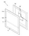
Translated fromKorean도 1은 유기 전계발광 소자의 개략적인 분해 사시도이다.1 is a schematic exploded perspective view of an organic electroluminescent device.
도 2는 도 1의 유기 전계발광 소자의 다른 사시도이다.FIG. 2 is another perspective view of the organic electroluminescent device of FIG. 1.
도 3은 도 1의 Ⅲ-Ⅲ 선을 따라 취한 부분 단면도이다.3 is a partial cross-sectional view taken along the line III-III of FIG. 1.
도 4는 봉지 수단과 전극 사이의 단락을 설명하는 개략도이다.4 is a schematic view illustrating a short circuit between the sealing means and the electrode.
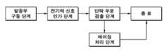
도 5는 본 발명에 따른 단락 부분 검출 및 수리 방법을 단계적으로 나타낸 블록도이다.5 is a block diagram showing a step-by-step detection and repair method according to the present invention.
<도면의 주요 부분에 대한 부호의 설명><Explanation of symbols for the main parts of the drawings>
100 : 유기 전계발광 소자110 : 기판100 organic
120 : 발광부130 : 봉지 수단120: light emitting unit 130: sealing means
136 : 밀봉재141, 143 : 전극136:
142 : 발광층151, 152 : 단자부142:
본 발명은 평판 표시 장치의 단락 부분 검출 및 수리 방법에 관한 것으로서, 보다 상세하게는, 유기 전계발광 소자에 구비되는 봉지 수단과 전극 사이의 단락 부분을 간단하게 검출하고 신속하게 수리할 수 있는 방법에 관한 것이다.BACKGROUND OF THE INVENTION 1. Field of the Invention The present invention relates to a method for detecting and repairing a short circuit portion of a flat panel display device, and more particularly, to a method for easily detecting and quickly repairing a short circuit portion between an encapsulation means and an electrode provided in an organic electroluminescent element. It is about.
최근, 기존의 음극선관을 대체할 수 있는 다양한 평판 표시 장치가 개발 및 생산 중에 있으며, 그 예로서 전계발광 디스플레이(Electroluminescent display : ELD)가 있다. 전계발광 디스플레이는 발광층을 구성하는 물질에 따라 유기 전계발광 소자와 무기 전계발광 소자로 크게 구분된다. 이 중 유기 전계발광 소자(OLED)는 솔리드 스테이트(solid state) 특성을 가져 사용 온도 범위가 넓고 내충격성 및 내진동성이 강하며, 시야각이 넓고 응답속도가 우수하며 컬러 디스플레이가 가능하다는 장점이 있어서 고성능의 평판 표시 장치로서 각광을 받고있으며, 휴대전화 또는 개인휴대단말기(PDA) 등의 표시 패널로서 사용되고 있다Recently, various flat panel display devices that can replace the existing cathode ray tube are being developed and produced, for example, an electroluminescent display (ELD). Electroluminescent displays are largely classified into organic electroluminescent devices and inorganic electroluminescent devices according to materials constituting the light emitting layer. Among them, the organic electroluminescent device (OLED) has a solid state characteristic, which has a wide range of operating temperature, high impact resistance and vibration resistance, a wide viewing angle, excellent response speed, and color display, thereby enabling high performance. Is gaining popularity as a flat panel display device, and is used as a display panel for a mobile phone or a personal digital assistant (PDA).
일반적으로 이러한 유기 전계발광 소자는 투명한 절연기판 상에 소정 패턴으로 형성된 애노드 전극의 제1전극층, 제1전극층 상에 형성된 발광재료를 포함하는 유기발광층 및 유기발광층 상에 형성된 캐소드 전극의 제2전극층을 구비하고, 이러한 유기발광층과 전극층을 외부의 산소나 습기로부터 차단하여 보호하도록 봉지 수단이 기판 상에 설치된다.In general, such an organic electroluminescent device includes a first electrode layer of an anode electrode formed in a predetermined pattern on a transparent insulating substrate, an organic light emitting layer including a light emitting material formed on the first electrode layer, and a second electrode layer of a cathode electrode formed on the organic light emitting layer. And an encapsulation means is provided on the substrate to shield and protect the organic light emitting layer and the electrode layer from external oxygen or moisture.
이러한 유기 전계발광 소자는 애노드 전극에 캐소드 전극보다 높은 전압을 인가하면 정공이 제1전극층에서 유기발광층으로 이동하고 전자가 제2전극층에서 유기발광층으로 이동되며, 이동된 정공 및 전자는 유기발광층에서 재결합하여 여기자를 형성하고 이 여기자로부터의 에너지에 의해 특정 파장의 빛이 발생하여 발광을 실행한다.In the organic electroluminescent device, when a voltage higher than the cathode is applied to the anode, holes move from the first electrode layer to the organic light emitting layer, electrons move from the second electrode layer to the organic light emitting layer, and the moved holes and electrons recombine in the organic light emitting layer. To form an exciton, and light of a specific wavelength is generated by energy from the exciton to emit light.
유기발광층과 전극층을 보호하는 봉지 수단은 플라스틱 또는 금속을 재료로 하여 형성될 수 있다. 이 봉지 수단의 가장자리를 따라서 밀봉재를 도포한 후 봉지 수단이 기판과 결합된다. 이 과정에서, 특히 봉지 수단이 금속으로 이루어진 경우, 밀봉재의 불량 등으로 인해 봉지 수단과 전극 사이에 국부적으로 단락이 발생할 수 있으며, 이러한 단락은 제품 불량을 초래하여 전체 소자를 폐기해야 하는 문제가 발생할 수 있다.The encapsulation means for protecting the organic light emitting layer and the electrode layer may be formed of plastic or metal. After applying the sealing material along the edge of the sealing means, the sealing means is combined with the substrate. In this process, in particular, when the sealing means is made of metal, a short circuit may occur locally between the sealing means and the electrode due to a failure of the sealing material, and such a short circuit may cause a product defect and cause a problem that the entire device must be disposed of. Can be.
본 발명은 위와 같은 문제점을 해결하기 위하여 창안된 것으로서, 봉지 수단과 전극 사이의 단락 부분을 간단한 절차에 의해 검출하고 즉시 수리할 수 있는 단락 부분 검출 및 수리 방법을 제공하는데 그 목적이 있다.The present invention was devised to solve the above problems, and an object thereof is to provide a short-circuit detection and repair method capable of immediately detecting and repairing a short-circuit between the sealing means and the electrode by a simple procedure.
위와 같은 목적 및 그 밖의 다른 목적을 달성하기 위하여, 본 발명의 평판 표시 장치의 단락 부분 검출 및 수리 방법은, 기판과, 발광층 및 상기 발광층을 작동시키는 다수의 전극을 가지는 발광부와, 상기 발광부를 덮어 보호하도록 상기 기판에 접합된 봉지수단을 구비하는 평판 표시 장치의 상기 봉지수단과 상기 전극 사이의 단락 부분을 검출하고 수리하는 방법으로서, 상기 발광부를 구동시키는 단계와, 상기 봉지수단과 상기 전극 사이에 전기적 신호를 인가하는 단계와, 상기 발광부의 변화를 확인하여 단락 부분을 검출하는 단계와, 상기 단락 부분을 수리하는 단계를 포함한다.In order to achieve the above and other objects, the short-circuit detection and repair method of the flat panel display device of the present invention, the light emitting portion having a substrate, a light emitting layer and a plurality of electrodes for operating the light emitting layer, and the light emitting portion A method of detecting and repairing a short circuit portion between the encapsulation means and the electrode of a flat panel display device having encapsulation means bonded to the substrate to cover and protect the device, the method comprising: driving the light emitting unit; Applying an electrical signal to the signal, checking a change in the light emitting part, detecting a short circuit part, and repairing the short circuit part.
또한, 상기 전극은 애노드 전극으로서 기능하는 제1전극과 캐소드 전극으로 서 기능하는 제2전극을 구비하고, 상기 평판 표시 장치는 상기 봉지 수단으 일측으로부터 연장되고 상기 발광부에 구비된 전극에 접속된 단자부를 더 구비하며, 상기 단자부는 상기 제1전극에 접속된 제1단자부와 상기 제2전극에 접속된 제2단자부를 구비할 수 있다.The electrode may include a first electrode functioning as an anode electrode and a second electrode functioning as a cathode electrode, and the flat panel display device may extend from one side of the encapsulation means and be connected to an electrode provided in the light emitting part. The terminal unit may further include a first terminal unit connected to the first electrode and a second terminal unit connected to the second electrode.
이와 같은 본 발명에 따른 단락 부분 검출 및 수리 방법에 의하면, 발광부를 구동시킨 상태에서 봉지 수단과 단자부 사이에 전기적 신호를 인가하고, 발광부에 나타난 변화를 확인하여 소정 부분의 단락을 검출하므로 신속하고 정확하게 단락 부분을 검출할 수 있고 검출된 단락 부분에 소정의 조치를 취하여 즉시 수리할 수 있다.According to the short-circuit detection and repair method according to the present invention, since the electrical signal is applied between the encapsulation means and the terminal portion while the light-emitting portion is driven, the short-circuit of the predetermined portion is detected by checking the change shown in the light-emitting portion. The short circuit part can be detected accurately and the repair can be performed immediately by taking a predetermined action on the detected short circuit part.
또한, 상기 전기적 신호 인가 단계는 상기 봉지수단과 상기 제1단자부 또는 상기 제2단자부 중에서 선택되는 어느 하나의 단자부에 전기적 신호를 인가하는 단계를 구비하는 것이 바람직하다.The applying of the electrical signal may preferably include applying an electrical signal to any one terminal unit selected from the encapsulation means and the first terminal portion or the second terminal portion.
여기서, 상기 전기적 신호 인가 단계는 선택된 단자부를 따라가면서 상기 봉지수단과 상기 단자부 사이에 전기적 신호를 인가하는 단계인 것이 바람직하다. 또한, 상기 단락 부분 검출 단계는, 상기 봉지수단과 상기 단자부 사이에 전기적 신호를 인가하여 상기 발광부의 휘도 변화가 나타난 부분에 해당하는 단자부에 연결된 전극이 상기 봉지수단과 단락된 것으로 결정하여 단락 부분을 검출하는 것이 바람직하다.Here, the step of applying the electrical signal is preferably a step of applying an electrical signal between the sealing means and the terminal portion while following the selected terminal portion. In the detecting of the short circuit portion, an electrical signal is applied between the encapsulation means and the terminal portion to determine that an electrode connected to the terminal portion corresponding to the portion where the luminance change of the light emitting portion is displayed is shorted with the encapsulation means. It is desirable to detect.
이 경우, 선택된 단자부를 따라가면서 봉지 수단과 이 단자부에 전기적 신호를 인가하게 되면, 단락된 부분에 전기적 신호가 인가될 경우 발광부에 휘도 변화 가 나타나게 되고, 이 때의 해당 단자부와 봉지 수단이 단락된 것으로 결정할 수 있다. 이 때, 상기 발광부에 나타나는 휘도 변화는 명선 형태 또는 암선 형태 중 어느 하나의 형태가 될 수 있다.In this case, when an electric signal is applied to the sealing means and the terminal part while following the selected terminal part, a luminance change appears in the light emitting part when an electrical signal is applied to the shorted part, and the corresponding terminal part and the sealing means are short-circuited at this time. Can be determined. In this case, the luminance change appearing in the light emitting part may be in the form of either bright or dark lines.
또한, 상기 단락 부분 수리 단계는 단락된 전극과 상기 봉지수단에 전기적 신호를 인가하는 에이징 처리에 의해 실행되는 것이 바람직하다.The short-circuit repair step is preferably carried out by an aging process for applying an electrical signal to the shorted electrode and the sealing means.
이 경우, 검출된 단락 부분에 소정 전기적 신호를 다시 인가하여 단락을 유발한 도전성 물질을 열화시키거나 에이징시킴으로써 단락된 부분을 수리할 수 있다.In this case, the shorted portion can be repaired by applying a predetermined electrical signal to the detected shorted portion again to degrade or age the conductive material causing the short circuit.
또한, 상기 전기적 신호는 접지, DC, AC 또는 펄스 중에서 선택되는 어느 하나인 것이 바람직하다.In addition, the electrical signal is preferably any one selected from ground, DC, AC or pulse.
또한, 상기 평판 표시 장치는 유기 전계발광 소자가 될 수 있다.In addition, the flat panel display may be an organic electroluminescent device.
이하에서는, 첨부된 도면을 참조하여 본 발명의 바람직한 실시예에 따른 평판 표시 장치의 단락 부분 검출 방법 및 수리 방법에 대해 상세하게 설명하며, 특히 평판 표시 장치 중 유기 전계발광 소자를 예로 들어 설명한다.Hereinafter, a short-circuit detection method and a repairing method of a flat panel display device according to an exemplary embodiment of the present invention will be described in detail with reference to the accompanying drawings. In particular, an organic electroluminescent device of the flat panel display device will be described as an example.
도 1은 평판 표시 장치의 일 예인 유기 전계발광 소자의 개략적인 분해 사시도이고, 도 2는 도 1의 유기 전계발광 소자의 다른 사시도이고, 도 3은 도 2의 Ⅲ-Ⅲ 선을 따라 취한 부분 단면도이며, 이들 도면에서 동일하게 부여된 참조번호는 동일한 부재를 지칭한다.1 is a schematic exploded perspective view of an organic electroluminescent device as an example of a flat panel display, FIG. 2 is another perspective view of the organic electroluminescent device of FIG. 1, and FIG. 3 is a partial cross-sectional view taken along line III-III of FIG. 2. Like reference numerals in the drawings denote like elements.
도면을 참조하면, 유기 전계발광 소자(100)는 기판(110)과, 소정의 화상을 구현할 수 있는 발광부(120)와, 발광부(120)를 덮어서 보호하도록 기판(110) 상에 설치되는 봉지 수단(130)을 구비하며, 봉지 수단(130)의 일측으로부터 연장되고 상기 발광부(120)에 구비된 다수의 전극에 접속된 단자부(151, 152)가 더 구비되어 있다.Referring to the drawings, the organic
상기 기판(110)은 유리, 플라스틱 또는 스테인리스스틸과 같은 금속으로 이루어질 수 있다. 여기서, 유기 전계발광 소자가 수동 구동형(passive matrix type)인 경우에는 기판(110)은 SiO2 등으로 이루어질 수 있는 버퍼층을 구비한 단일의 평판이 될 수도 있고, 능동 구동형(active matrix type)인 경우에는 기판(110)은 발광부(120)를 구동하기 위한 픽셀 회로를 구비할 수 있다.The
상기 봉지 수단(130)은 발광부(120)를 외부의 수분 또는 산소로부터 보호하여 발광부의 열화와 발광부를 구성하는 구성요소간의 박리를 방지하기 위해 설치되는 것으로서, 투명 유리 또는 플라스틱으로 이루어질 수도 있고, 금속으로 이루어질 수도 있다. 예컨대, 전면 발광 방식의 발광부(120)를 구성하는 경우에는, 봉지 수단(130)은 투명한 유리 또는 플라스틱으로 상기 기판(110)과 동일한 재료로 형성될 수도 있고, 배면 발광 방식으로 발광부(120)를 구성하는 경우에는 금속으로 형성된 이른바 메탈캡이 될 수도 있다.The encapsulation means 130 is installed to protect the
상기 봉지 수단(130)은 밀봉재(136)를 통해 상기 기판(110) 상에 설치된다. 또한, 선택적으로, 상기 봉지 수단(130)에는 그 내부 공간의 습기를 흡수하기 위해 분말상의 흡습재(135)가 오목부(131) 내에 더 구비될 수 있다. 흡습재(135)가 더 구비된 봉지 수단(130)은 배면 발광 방식의 경우에 적합할 수 있다.The encapsulation means 130 is installed on the
상기 발광부(140)는 문자나 기호 등의 심벌과 화상을 구현하기 위한 요소로서 단일의 표시부로서 구성될 수도 있거나 혹은 심벌을 주로 표시하는 아이콘 표시부와 정지화상 및 동화상을 표시하는 화상 표시부로 구분되어 구성될 수도 있다. 도 3에 도시된 바와 같이, 상기 발광부(140)는 서로 대향된 제1전극(141) 및 제2전극(142)과 이들 전극 사이에 개재된 발광층(143)을 구비한다. 상세하게는, 상기 발광부(140)는 서로 소정 간격으로 이격되어 스트라이프 형상으로 형성된 제1전극(141)과, 상기 제1전극(141)을 소정의 패턴으로 구획하는 절연층(145)과, 상기 기판(110)의 상면에 노출된 제1전극(141)들의 상면에 소정 패턴으로 증착되는 발광층(143)과, 상기 제1전극(141)과 절연되어 있고 상기 발광층(143)의 상방에 형성된 제2전극(142)을 구비하며, 상기 발광부(140)는 위에서 기술된 방식으로 형성되는 것에 한정되지 않고 다양한 패턴으로 형성하는 것이 가능하다.The light emitting unit 140 may be configured as a single display unit as an element for embodying a symbol and an image such as a character or a symbol, or is divided into an icon display unit that mainly displays a symbol and an image display unit that displays still and moving images. It may be configured. As illustrated in FIG. 3, the light emitting unit 140 includes a
상기 제1전극(141)은 애노드 전극으로서 기능하고, 대향된 제2전극(142)은 캐소드 전극으로 기능할 수 있으며, 이들 전극(141, 142)의 극성은 반대로 되어도 무방하다.The
상기 제1전극(141)은 유기 전계발광 소자가 배면 발광형인 겨우 투명 전극으로 형성될 수 있고, 전면 발광형인 경우 반사형 전극으로 형성될 수 있다. 투명 전극으로서 형성되는 경우에는, 상기 제1전극(141)은 ITO, IZO, ZnO 또는 In2O3 등으로 이루어질 수 있고, 반사형 전극으로서 형성되는 경우에는, Ag, Mg, Al, Pt, Pd, Au, Ni, Nd, Ir, Cr 및 이들의 화합물 등으로 반사막을 형성한 후, 그 위에 ITO, IZO, ZnO 또는 In2O3을 형성할 수도 있다. 또한, 상기 제1전극(141)은 유기 발광 소자가 수동 구동형인 경우 기판(110) 상에 직접 형성될 수도 있고, 능동 구동형인 경우 기판(110)에 구비된 구동용 박막트랜지스터의 소오스/드레인 전극 중 어느 하나에 접속되도록 형성될 수 있다.The
상기 제1전극(141)에 대향된 제2전극(142)도 투명 전극 또는 반사형 전극으로 형성될 수 있으며, 투명 전극으로 형성되는 경우에는, 상기 제2전극(142)이 캐소드 전극으로 사용되는 까닭에, 일함수가 작은 금속, 예컨대 Li, Ca, LiF/Ca, LiF/Al, Al, Mg 및 이들의 화합물이 발광층(142)을 향하도록 증착한 후, 그 위에 ITO, IZO, ZnO 또는 In2O3 등으로 형성될 수 있다. 또한, 반사형 전극으로 형성되는 경우에는, Li, Ca, LiF/Ca, LiF/Al, Al, Mg 및 이들의 화합물을 전면 증착하여 형성된다.The
상기 발광층(143)은 저분자 또는 고분자 유기층이 사용될 수 있다. 저분자 유기층을 사용할 경우, 발광층(143)은 홀 주입층(HIL: Hole Injection Layer), 홀 수송층(HTL: Hole Transport Layer), 유기 발광층(EML: Emission Layer), 전자 수송층(ETL: Electron Transport Layer), 전자 주입층(EIL: Electron Injection Layer) 등이 단일 혹은 복합 구조로 열거된 순서대로 적층되어 형성될 수 있고, 상기 제1전극(141) 및 제2전극(142)의 기능이 반대로 된 경우, 즉 제1전극(141)이 캐소드 전극이고 제2전극(142)이 애노드 전극인 경우에는 발광층(142)은 위에서 열거된 순서의 역으로 적층되어 형성될 수도 있으며, 사용 가능한 유기 재료도 구리 프 탈로시아닌(CuPc: copper phthalocyanine), N,N-디(나프탈렌-1-일)-N,N'-디페닐-벤지딘(N,N'-Di(naphthalene-1-yl)-N,N'-diphenyl-benzidine: NPB), 트리스-8-하이드록시퀴놀린 알루미늄(tris-8-hydroxyquinoline aluminum)(Alq3) 등을 비롯해 다양하게 적용 가능하다. 이들 저분자 유기층은 진공증착의 방법으로 형성된다.The
고분자 유기층의 경우, 발광층(143)은 대개 홀 수송층(HTL) 및 발광층(EML)을 구비한 구조를 가질 수 있으며, 이 때, 상기 홀 수송층으로 PEDOT를 사용하고, 발광층으로 PPV(Poly-Phenylenevinylene)계 및 폴리플루오렌(Polyfluorene)계 등 고분자 유기물질을 사용하며, 이를 스크린 인쇄나 잉크젯 인쇄 방법 등으로 형성할 수 있다.In the case of the polymer organic layer, the
이들 전극(141, 142)에 접속되어 외부의 전원 또는 제어 회로에 연결시키기 위한 단자부(151, 152)가 상기 봉지 수단(130)의 일측으로부터 인출되도록 구성되어 있다. 도 3에는, 제1전극(141)이 발광부(140)의 외측으로 연장되어 단자부(151)에 접속되어 있는 것으로 도시되어 있지만, 이것은 단지 예시적인 것으로서, 단자부와 전극 사이의 접속은 다양한 형태를 취할 수 있다. 예컨대, 발광부(140) 내측에만 제1전극(141)을 한정하고 이 전극과 단자부(151) 사이를 도전성의 라인(미도시)을 통해 접속시킬 수도 있으며, 이러한 다양한 구성은 제2전극(142)과 단자부(152)의 경우에도 마찬가지이다.
도 2에는, 발광부(140) 내에 구비된 제1전극(141)에 접속된 제1전극 단자부(151)가 봉지 수단(130)의 일측으로부터 인출되어 있고, 제2전극(142)에 접속된 제2전극 단자부(152)는 제1전극 단자부(152)와는 다른 측에서 상기 봉지 수단(130)으 로부터 인출되어 있다. 이러한 단자부들(151, 152)의 인출 방향이 도 2에 도시된 형태에 한정되는 것은 아니고, 유기 전계발광 소자가 채용될 수 있는 표시 장치의 설계 유형에 따라 다양하게 변형될 수 있으며, 예컨대 상기 단자부들(151, 152)은 봉지 수단(130)의 동일한 측면으로부터 인출될 수도 있고, 혹은 봉지 수단(130)의 대향된 측면으로부터 각기 인출될 수도 있다.In FIG. 2, the first
위에서 기술한 바와 같이, 봉지 수단(130)은 밀봉재(136)를 통해 상기 기판(110) 상에 설치된다. 상세하게는, 도 2 및 도 3으로부터 알 수 있는 바와 같이, 봉지 수단(130)은 기판(110)과 전극(141 또는 142)에 모두 걸치는 밀봉재(136)를 통해 기판(110)에 설치된다. 봉지 수단(130)과 전극(141 또는 142)은 상기 밀봉재(136) 내에 포함된 도전성 물질을 통해 서로 단락될 가능성이 있다. 특히, 금속을 재료로 한 메탈캡과 같은 봉지 수단(130)이 사용되는 경우, 봉지 수단(130)과 전극(141 또는 142)이 단락으로 인해 평판 표시 장치, 예컨대 유기 전계발광 소자(100)는 소정의 화상을 신뢰성 높게 구현할 수 없게 되므로, 이러한 단락 부분을 검출하고 신속하게 수리할 필요가 있다.As described above, the sealing means 130 is installed on the
도 4는 봉지 수단과 전극 사이의 단락을 설명하는 도면이고, 도 5는 본 발명에 따른 단락 부분 검출 및 수리 방법을 단계적으로 나타낸 블록도이다.4 is a diagram illustrating a short circuit between the encapsulation means and the electrode, and FIG. 5 is a block diagram illustrating a method of detecting and repairing a short circuit part according to the present invention.
봉지 수단(130)이 전극(141 또는 142)과 단락되면, 도 4와 같이 봉지 수단(130)이 데이터 라인 또는 스캔 라인과 단락된 것으로 표시될 수 있다. 여기서, 양방향 화살표로 나타낸 것은 봉지 수단(130)이 데이터 라인 또는 스캔 라인을 이루는 전극과 단락될 수 있음으로 나타낸다. 즉, 봉지 수단(130)은 데이터 라인을 구성하는 전극(예컨대, 제1전극) 또는 스캔 라인을 구성하는 전극(예컨대, 제2전극) 중 어느 하나 또는 양자에 모두 단락될 수 있으며, 이러한 단락 과정은 위에서 이미 설명하였다.When the encapsulation means 130 is shorted with the
도 4에서 알 수 있듯이, 유기 전계발광 소자(OLED)가 구동된 상태에서 봉지 수단(130)과 데이터 라인을 구성하는 전극들 또는 스캔 라인을 구성하는 전극들 중 어느 하나에 전기적 신호를 인가하면, 이 인가된 전기적 신호에 의해 발광부(120)에 변화가 나타난다. 본 발명은 발광부(120)에 나타난 변화를 확인하여 신속하고 정확하게 봉지 수단(130)과 전극(141, 142) 사이의 단락 부분을 검출할 수 있다.As can be seen in FIG. 4, when the organic electroluminescent device OLED is driven, an electrical signal is applied to either the encapsulation means 130 and the electrodes constituting the data line or the electrodes constituting the scan line. A change appears in the
도 5를 참조하면, 본 발명에 따른 단락 부분 검출 및 수리 방법은 크게 발광부를 구동하는 단계와, 봉지 수단과 전극(바람직하게는, 해당 전극에 접속된 단자부) 사이에 전기적 신호를 인가하는 단계와, 발광부에 나타난 변화를 확인하여 전기적 신호가 인가된 부분의 전극의 단락 여부를 검출하는 단계와, 해당 전극이 단락된 것으로 판정되면 전기적 신호를 다시 인가하여 단락 부분을 수리하는 단계를 포함한다.Referring to FIG. 5, the method for detecting and repairing a short-circuit portion according to the present invention includes driving a light emitting unit largely, applying an electrical signal between an encapsulation means and an electrode (preferably, a terminal portion connected to the corresponding electrode); And checking whether the electrode is short-circuited by checking the change in the light emitting part, and repairing the short-circuit by applying the electrical signal again when it is determined that the electrode is short-circuited.
도 1 내지 도 3과 관련하여 설명한 평판 표시 장치, 예컨대 유기 전계발광 소자에 통상의 구동 전압을 인가하여 발광부(120)를 구동시킨다.The
그 후, 유기 전계발광 소자(OLED)가 구동된 상태, 즉 발광부(120)가 켜져 있는 상태에서, 전극들 중 일부와 봉지 수단 사이에 전기적 신호를 인가한다. 이 때 인가되는 전기적 신호는 접지, DC, AC 또는 펄스 중에서 선택되는 어느 하나인 것이 바람직하며, 인가되는 전압 범위는 수 십 내지 수 백 볼트가 가능하다.Thereafter, an electric signal is applied between some of the electrodes and the encapsulation means while the organic electroluminescent element OLED is driven, that is, the
전극들 중 일부가 봉지 수단과 단락되어 있고 이 단락된 전극과 봉지 수단에 전기적 신호가 인가되면, 발광부(120)에는 단락 때문에 추가로 인가된 전기적 신호에 의해 변화가 나타날 수 있으며, 이 변화는 도 1에 도시된 바와 같은 선의 형상(L1 또는 L2)으로서 발광부(120)에 나타날 수 있다.If some of the electrodes are short-circuited with the encapsulation means and an electrical signal is applied to the shorted electrodes and the encapsulation means, a change may appear in the
발광부(120) 내에 구비된 전극(141 또는 142)은, 유기 전계발광 소자가 PM 구동 방식인 경우 예컨대 스트라이프 형태로 설치될 것이고 AM 구동 방식인 경우에도 전극(141, 142) 중의 하나 또는 둘 다는 각 픽셀에만 형성되어도 그 전체로는 데이터 라인 또는 스캔 라인을 형성하도록 일 직선의 형태가 될 것이므로, 봉지 수단(130)과 접속된 전극에 전기적 신호가 인가되면, 발광부(120)에는 선 형태의 휘도의 변화가 나타나게 된다.The
여기서, 선(L1, L2)은 ‘암선’ 또는 ‘명선’이 될 수 있으며, 암선은 주변 보다 어두운 밝기의 선 형상을 의미하고, 명선은 주변 보다 밝은 밝기의 선 형상을 의미한다.Here, the lines L1 and L2 may be 'dark lines' or 'bright lines', and the dark lines mean a line shape having a darker brightness than the surroundings, and the bright line means a line shape having a brighter brightness than the surroundings.
이렇게 하여, 봉지 수단(130)과 전극(141, 142) 사이의 단락된 부분에 전기적 신호가 인가되면, 발광부(120)에 나타난 암선 또는 명선(L1 또는 L2)을 확인함으로써, 봉지 수단(130)과 전극(141, 142) 사이의 단락된 부분을 시각적으로 용이하게 검출할 수 있다.In this way, when an electrical signal is applied to the shorted part between the sealing means 130 and the
보다 상세하게는, 발광부(120)가 구동되어 소정 밝기의 휘도로 발광하는 상태에서, 봉지 수단(130)과 전극(141 또는 142)(바람직하게는, 해당 전극에 접속된 단자부(151 또는 152))에 전기적 신호를 인가한다. 이 경우, 단자부(151 또는 152)의 일측 단부로부터 순차적으로 전기적 신호를 인가한다. 단자부의 어느 일측단부로부터 순차적으로 전기적 신호를 인가해 가는 동시에 발광부(120)의 변화를 확인한다. 순차적으로 단자부를 따라 가면서 전기적 신호를 인가해 가는 도중 발광부(120)에 암선 또는 명선의 형태로서 휘도의 변화가 발생하면, 이 순간에 전기적 신호가 인가된 전극이 봉지 수단(130)과 단락되어 있음을 의미하므로, 이 때의 전극을 단락된 전극으로 판정한다. 계속해서 나머지 단자부를 따라 가면서 단락 부분 검출 과정을 계속 수행하여, 나머지 부분에서도 있을 수 있는 봉지 수단과 단락된 전극을 검출 할 수 있다.More specifically, the sealing
그 후, 봉지 수단(130)과 단락된 것으로 판정된 전극을 수리한다. 봉지 수단과 전극 사이의 단락은 위에서 설명한 대로 밀봉재(136) 내에 포함된 도전성 물질에 의해 기인할 수 있다. 따라서, 이러한 단락을 유발시킨 도전성 물질을 열화시킴으로써 봉지 수단과 전극 사이의 단락이 해제될 수 있다. 이를 위해, 단락된 전극과 봉지 수단에 전기적 신호를 재인가하여 단락을 유발한 도전성 물질을 전기적 에이징 처리에 의해 열화시킨다. 즉, 전기적 에이징 처리를 하면, 인가된 전기적 신호에 의해 단락을 유발한 도전성 물질이 가열되어 열화됨으로써, 도전성 물질에 의한 봉지 수단(130)과 전극 사이의 단락이 해제될 수 있다.Then, the electrode determined to be short-circuited with the sealing means 130 is repaired. The short circuit between the encapsulation means and the electrode may be due to the conductive material included in the
또한, 재인가되는 전기적 신호는 단락 부분을 검출하기 위해 인가되는 전기적 신호의 크기와 동일하거나 혹은 보다 클 수 있다. 또한, 이러한 수리 단계는 모든 단락 부분을 검출한 후 별개로 수행될 수도 있고, 단자부를 따라 가면서 단락 부분이 검출될 때 즉시 수행될 수도 있다.In addition, the reapplied electrical signal may be equal to or greater than the magnitude of the electrical signal applied to detect the short circuit portion. In addition, this repair step may be performed separately after detecting all short-circuits, or may be performed immediately when a short-circuit is detected while following the terminal section.
한편, 도 2에 도시된 평판 표시 장치의 일 예인 유기 전계발광 소자(100)는 최종 완성된 형태의 모듈로서, 이러한 유기 전계발광 소자는 대형의 기판 상에 다수의 발광부를 형성한 후 소정 길이로 기판을 절단하여 제조될 수 있다. 따라서, 본 발명에 따른 단락 부분 검출 및 수리 방법은 도 2에 도시된 최종 완성된 모듈 상태에서 실행될 수도 있고, 아울러 이러한 모듈 상태의 유기 전계발광 소자(100)가 기판으로 절단되기 전인 기판 상태에서도 수행될 수 있다.Meanwhile, the
위에서 설명한 바와 같이 본 발명에 따른 평판 표시 장치의 단락 부분 검출 및 수리 방법에 의하면, 발광부를 봉지하는 봉지 수단과 발광부 내에 구비된 전극 사이의 단락을 전기적 신호에 의해 나타난 발광부의 변화를 확인하여 신속하고 간단하게 검출하고, 아울러 검출된 단락 부분의 도전성 물질을 전기적 에이징 처리에 의해 열화시켜 단락 부분을 수리하여, 봉지 수단과 전극 사이의 단락으로 인한 제품 불량을 해결할 수 있다.As described above, according to the method for detecting and repairing a short circuit portion of the flat panel display device according to the present invention, a short circuit between the sealing means for encapsulating the light emitting portion and the electrode provided in the light emitting portion is quick to check the change of the light emitting portion indicated by the electrical signal. In addition, it is possible to simply detect and deteriorate the conductive material of the detected short-circuit portion by an electrical aging treatment to repair the short-circuit portion, thereby solving product defects due to a short circuit between the sealing means and the electrode.
본 발명은 도면에 도시된 실시예를 참고로 설명되었으나 이는 예시적인 것에 불과하며, 본 기술 분야의 통상의 지식을 가진 자라면 이로부터 다양한 변형 및 균등한 다른 실시예가 가능하다는 점을 이해할 것이다. 따라서, 본 발명의 진정한 기술적 보호 범위는 첨부된 특허청구범위의 기술적 사상에 의하여 정해져야 할 것이다.Although the present invention has been described with reference to the embodiments shown in the drawings, this is merely exemplary, and it will be understood by those skilled in the art that various modifications and equivalent other embodiments are possible. Therefore, the true technical protection scope of the present invention will be defined by the technical spirit of the appended claims.
Claims (9)
Translated fromKoreanPriority Applications (1)
| Application Number | Priority Date | Filing Date | Title |
|---|---|---|---|
| KR1020050038976AKR100626078B1 (en) | 2005-05-10 | 2005-05-10 | How to detect and repair short circuit in flat panel display |
Applications Claiming Priority (1)
| Application Number | Priority Date | Filing Date | Title |
|---|---|---|---|
| KR1020050038976AKR100626078B1 (en) | 2005-05-10 | 2005-05-10 | How to detect and repair short circuit in flat panel display |
Publications (1)
| Publication Number | Publication Date |
|---|---|
| KR100626078B1true KR100626078B1 (en) | 2006-09-20 |
Family
ID=37631867
Family Applications (1)
| Application Number | Title | Priority Date | Filing Date |
|---|---|---|---|
| KR1020050038976AExpired - Fee RelatedKR100626078B1 (en) | 2005-05-10 | 2005-05-10 | How to detect and repair short circuit in flat panel display |
Country Status (1)
| Country | Link |
|---|---|
| KR (1) | KR100626078B1 (en) |
Cited By (1)
| Publication number | Priority date | Publication date | Assignee | Title |
|---|---|---|---|---|
| KR20160038234A (en)* | 2014-09-30 | 2016-04-07 | 엘지디스플레이 주식회사 | Organic light emitting display device and methode of manufacturing the same |
Citations (1)
| Publication number | Priority date | Publication date | Assignee | Title |
|---|---|---|---|---|
| JP2003234187A (en) | 2001-12-06 | 2003-08-22 | Fuji Electric Co Ltd | Passive matrix organic thin-film light emitting display and repair method thereof |
- 2005
- 2005-05-10KRKR1020050038976Apatent/KR100626078B1/ennot_activeExpired - Fee Related
Patent Citations (1)
| Publication number | Priority date | Publication date | Assignee | Title |
|---|---|---|---|---|
| JP2003234187A (en) | 2001-12-06 | 2003-08-22 | Fuji Electric Co Ltd | Passive matrix organic thin-film light emitting display and repair method thereof |
Cited By (2)
| Publication number | Priority date | Publication date | Assignee | Title |
|---|---|---|---|---|
| KR20160038234A (en)* | 2014-09-30 | 2016-04-07 | 엘지디스플레이 주식회사 | Organic light emitting display device and methode of manufacturing the same |
| KR102343754B1 (en) | 2014-09-30 | 2021-12-24 | 엘지디스플레이 주식회사 | Organic light emitting display device and methode of manufacturing the same |
Similar Documents
| Publication | Publication Date | Title |
|---|---|---|
| KR102845512B1 (en) | Display device | |
| JP5969450B2 (en) | Organic light emitting display device and method for manufacturing organic light emitting display device | |
| JP3940738B2 (en) | Electroluminescent display device | |
| US8421097B2 (en) | Organic light emitting diode display device | |
| US9083002B2 (en) | Organic light-emitting display device | |
| KR102038983B1 (en) | Organic light emitting display apparatus, method for inspecting the organic light emitting display apparatus and apparatus for inspeting the organic light emitting display apparatus | |
| KR102443645B1 (en) | Organic light emitting diode display and manufacturing method thereof | |
| US8998446B2 (en) | Optical film and organic light emitting display apparatus comprising the same | |
| US20080239637A1 (en) | Display device and method of manufacturing the same | |
| US20120007107A1 (en) | Organic light emitting diode display and manufacturing method thereof | |
| US8223095B2 (en) | Organic light-emitting display device having a pixel unit for testing pixels of the display device | |
| US9269756B2 (en) | Organic light emitting display apparatus | |
| JP2012094513A (en) | Organic light-emitting display device | |
| US7863810B2 (en) | Organic light emitting display device | |
| WO2008016279A1 (en) | Organic light emitting device | |
| KR100626078B1 (en) | How to detect and repair short circuit in flat panel display | |
| KR100719537B1 (en) | Flat panel displays and substrates for flat panel displays | |
| KR100669740B1 (en) | Flat panel display | |
| KR100528914B1 (en) | Organic electro luminescence display device | |
| KR20100009319A (en) | Organic light emitting display apparatus and method of manufacturing thereof | |
| KR100719599B1 (en) | Flat panel display device | |
| JP4770523B2 (en) | Method for manufacturing light emitting device | |
| KR100659106B1 (en) | Organic light emitting display | |
| US20240155874A1 (en) | Display device and method of manufacturing display device | |
| JP2008071578A (en) | Organic EL display device |
Legal Events
| Date | Code | Title | Description |
|---|---|---|---|
| A201 | Request for examination | ||
| PA0109 | Patent application | St.27 status event code:A-0-1-A10-A12-nap-PA0109 | |
| PA0201 | Request for examination | St.27 status event code:A-1-2-D10-D11-exm-PA0201 | |
| R17-X000 | Change to representative recorded | St.27 status event code:A-3-3-R10-R17-oth-X000 | |
| D13-X000 | Search requested | St.27 status event code:A-1-2-D10-D13-srh-X000 | |
| D14-X000 | Search report completed | St.27 status event code:A-1-2-D10-D14-srh-X000 | |
| E701 | Decision to grant or registration of patent right | ||
| PE0701 | Decision of registration | St.27 status event code:A-1-2-D10-D22-exm-PE0701 | |
| GRNT | Written decision to grant | ||
| PR0701 | Registration of establishment | St.27 status event code:A-2-4-F10-F11-exm-PR0701 | |
| PR1002 | Payment of registration fee | Fee payment year number:1 St.27 status event code:A-2-2-U10-U11-oth-PR1002 | |
| PG1601 | Publication of registration | St.27 status event code:A-4-4-Q10-Q13-nap-PG1601 | |
| PN2301 | Change of applicant | St.27 status event code:A-5-5-R10-R11-asn-PN2301 | |
| PN2301 | Change of applicant | St.27 status event code:A-5-5-R10-R11-asn-PN2301 | |
| PN2301 | Change of applicant | St.27 status event code:A-5-5-R10-R14-asn-PN2301 | |
| R18-X000 | Changes to party contact information recorded | St.27 status event code:A-5-5-R10-R18-oth-X000 | |
| R18-X000 | Changes to party contact information recorded | St.27 status event code:A-5-5-R10-R18-oth-X000 | |
| PR1001 | Payment of annual fee | Fee payment year number:4 St.27 status event code:A-4-4-U10-U11-oth-PR1001 | |
| R18-X000 | Changes to party contact information recorded | St.27 status event code:A-5-5-R10-R18-oth-X000 | |
| PR1001 | Payment of annual fee | Fee payment year number:5 St.27 status event code:A-4-4-U10-U11-oth-PR1001 | |
| PR1001 | Payment of annual fee | Fee payment year number:6 St.27 status event code:A-4-4-U10-U11-oth-PR1001 | |
| PN2301 | Change of applicant | St.27 status event code:A-5-5-R10-R11-asn-PN2301 | |
| PN2301 | Change of applicant | St.27 status event code:A-5-5-R10-R14-asn-PN2301 | |
| FPAY | Annual fee payment | Payment date:20120906 Year of fee payment:7 | |
| PR1001 | Payment of annual fee | Fee payment year number:7 St.27 status event code:A-4-4-U10-U11-oth-PR1001 | |
| FPAY | Annual fee payment | Payment date:20130830 Year of fee payment:8 | |
| PR1001 | Payment of annual fee | Fee payment year number:8 St.27 status event code:A-4-4-U10-U11-oth-PR1001 | |
| R18-X000 | Changes to party contact information recorded | St.27 status event code:A-5-5-R10-R18-oth-X000 | |
| FPAY | Annual fee payment | Payment date:20140901 Year of fee payment:9 | |
| PR1001 | Payment of annual fee | Fee payment year number:9 St.27 status event code:A-4-4-U10-U11-oth-PR1001 | |
| R18-X000 | Changes to party contact information recorded | St.27 status event code:A-5-5-R10-R18-oth-X000 | |
| PR1001 | Payment of annual fee | Fee payment year number:10 St.27 status event code:A-4-4-U10-U11-oth-PR1001 | |
| LAPS | Lapse due to unpaid annual fee | ||
| PC1903 | Unpaid annual fee | Not in force date:20160914 Payment event data comment text:Termination Category : DEFAULT_OF_REGISTRATION_FEE St.27 status event code:A-4-4-U10-U13-oth-PC1903 | |
| P22-X000 | Classification modified | St.27 status event code:A-4-4-P10-P22-nap-X000 | |
| PC1903 | Unpaid annual fee | Ip right cessation event data comment text:Termination Category : DEFAULT_OF_REGISTRATION_FEE Not in force date:20160914 St.27 status event code:N-4-6-H10-H13-oth-PC1903 | |
| P22-X000 | Classification modified | St.27 status event code:A-4-4-P10-P22-nap-X000 | |
| R18-X000 | Changes to party contact information recorded | St.27 status event code:A-5-5-R10-R18-oth-X000 | |
| P22-X000 | Classification modified | St.27 status event code:A-4-4-P10-P22-nap-X000 | |
| P22-X000 | Classification modified | St.27 status event code:A-4-4-P10-P22-nap-X000 |