KR100624405B1 - Optical component mounting board and its manufacturing method - Google Patents
Optical component mounting board and its manufacturing methodDownload PDFInfo
- Publication number
- KR100624405B1 KR100624405B1KR1020020059779AKR20020059779AKR100624405B1KR 100624405 B1KR100624405 B1KR 100624405B1KR 1020020059779 AKR1020020059779 AKR 1020020059779AKR 20020059779 AKR20020059779 AKR 20020059779AKR 100624405 B1KR100624405 B1KR 100624405B1
- Authority
- KR
- South Korea
- Prior art keywords
- substrate
- optical component
- stopper
- groove
- mounting
- Prior art date
- Legal status (The legal status is an assumption and is not a legal conclusion. Google has not performed a legal analysis and makes no representation as to the accuracy of the status listed.)
- Expired - Fee Related
Links
Images


Classifications
- G—PHYSICS
- G02—OPTICS
- G02B—OPTICAL ELEMENTS, SYSTEMS OR APPARATUS
- G02B6/00—Light guides; Structural details of arrangements comprising light guides and other optical elements, e.g. couplings
- G02B6/24—Coupling light guides
- G02B6/42—Coupling light guides with opto-electronic elements
- G—PHYSICS
- G02—OPTICS
- G02B—OPTICAL ELEMENTS, SYSTEMS OR APPARATUS
- G02B6/00—Light guides; Structural details of arrangements comprising light guides and other optical elements, e.g. couplings
- G02B6/24—Coupling light guides
- G02B6/42—Coupling light guides with opto-electronic elements
- G02B6/4201—Packages, e.g. shape, construction, internal or external details
- G02B6/4219—Mechanical fixtures for holding or positioning the elements relative to each other in the couplings; Alignment methods for the elements, e.g. measuring or observing methods especially used therefor
- G02B6/4233—Active alignment along the optical axis and passive alignment perpendicular to the optical axis
- G—PHYSICS
- G02—OPTICS
- G02B—OPTICAL ELEMENTS, SYSTEMS OR APPARATUS
- G02B6/00—Light guides; Structural details of arrangements comprising light guides and other optical elements, e.g. couplings
- G02B6/24—Coupling light guides
- G02B6/42—Coupling light guides with opto-electronic elements
- G02B6/4201—Packages, e.g. shape, construction, internal or external details
- G02B6/4204—Packages, e.g. shape, construction, internal or external details the coupling comprising intermediate optical elements, e.g. lenses, holograms
- G02B6/4206—Optical features
- G—PHYSICS
- G02—OPTICS
- G02B—OPTICAL ELEMENTS, SYSTEMS OR APPARATUS
- G02B6/00—Light guides; Structural details of arrangements comprising light guides and other optical elements, e.g. couplings
- G02B6/24—Coupling light guides
- G02B6/36—Mechanical coupling means
- G02B6/3628—Mechanical coupling means for mounting fibres to supporting carriers
- G02B6/3648—Supporting carriers of a microbench type, i.e. with micromachined additional mechanical structures
- G02B6/3652—Supporting carriers of a microbench type, i.e. with micromachined additional mechanical structures the additional structures being prepositioning mounting areas, allowing only movement in one dimension, e.g. grooves, trenches or vias in the microbench surface, i.e. self aligning supporting carriers
- G—PHYSICS
- G02—OPTICS
- G02B—OPTICAL ELEMENTS, SYSTEMS OR APPARATUS
- G02B6/00—Light guides; Structural details of arrangements comprising light guides and other optical elements, e.g. couplings
- G02B6/24—Coupling light guides
- G02B6/36—Mechanical coupling means
- G02B6/3628—Mechanical coupling means for mounting fibres to supporting carriers
- G02B6/3684—Mechanical coupling means for mounting fibres to supporting carriers characterised by the manufacturing process of surface profiling of the supporting carrier
- G02B6/3692—Mechanical coupling means for mounting fibres to supporting carriers characterised by the manufacturing process of surface profiling of the supporting carrier with surface micromachining involving etching, e.g. wet or dry etching steps
Landscapes
- Physics & Mathematics (AREA)
- General Physics & Mathematics (AREA)
- Optics & Photonics (AREA)
- Optical Couplings Of Light Guides (AREA)
Abstract
Translated fromKoreanDescription
Translated fromKorean도 1은 종래의 광부품 실장용 기판을 보인 개략적인 사시도.1 is a schematic perspective view showing a substrate for mounting a conventional optical component.
도 2 및 도 3 각각은 종래의 광부품 실장용 기판에 원통형 렌즈를 실장한 모습을 보인 개략적인 사시도 및 단면도.2 and 3 are schematic perspective views and cross-sectional views showing a state in which a cylindrical lens is mounted on a conventional substrate for mounting an optical component.
도 4는 본 발명의 일 실시예에 따른 광부품 실장용 기판을 일 평면에서 본 개략적인 단면도.4 is a schematic cross-sectional view of an optical component mounting substrate according to an embodiment of the present invention, viewed from one plane;
도 5는 본 발명의 일 실시예에 따른 광부품 실장용 기판을 다른 평면에서 본 개략적인 단면도.Figure 5 is a schematic cross-sectional view of another optical component mounting substrate according to an embodiment of the present invention in a plan view.
도 6은 본 발명의 다른 실시예에 따른 광부품 실장용 기판을 일 평면에서 본 개략적인 단면도.6 is a schematic cross-sectional view of a substrate for mounting an optical component according to another embodiment of the present invention, viewed from one plane;
도 7은 본 발명의 다른 실시예에 따른 광부품 실장용 기판을 다른 평면에서 본 개략적인 단면도.Figure 7 is a schematic cross-sectional view of another optical component mounting substrate according to another embodiment of the present invention in a plan view.
도 8a 내지 도 8f 및, 도 9a 내지 도 9c는 본 발명의 일 실시예에 따른 광부품 실장용 기판 제조공정을 설명하기 위해 나타낸 도면.8A to 8F and FIGS. 9A to 9C are diagrams for explaining an optical component mounting substrate manufacturing process according to an embodiment of the present invention.
도 10a 내지 도 10g는 본 발명의 다른 실시예에 따른 광부품 실장용 기판 제조공정을 설명하기 위해 나타낸 도면.10A to 10G are diagrams for explaining an optical component mounting substrate manufacturing process according to another embodiment of the present invention.
도 11은 도 10c에 도시된 공정시의 광부품 실장용 기판을 보인 평면도.Fig. 11 is a plan view showing a substrate for mounting an optical component in the process shown in Fig. 10C.
도 12는 도 10g에 도시된 공정시의 광부품 실장용 기판을 보인 평면도.FIG. 12 is a plan view showing a substrate for mounting an optical component in the process shown in FIG. 10G; FIG.
<도면의 주요 부분에 대한 부호의 설명><Explanation of symbols for the main parts of the drawings>
30, 51, 71...기판 31...그루브30, 51, 71
35, 37, 59, 77...스토퍼 41...원통형 렌즈35, 37, 59, 77
53, 79...포토레지스트 55,58...마스크53, 79
57, 73...폴리머층57, 73 ... polymer layer
본 발명은 광부품을 실장하는 광부품 실장용 기판 및 그 제조방법에 관한 것으로, 상세하게는 원통형 렌즈를 수동으로 보다 정확한 위치에 어라인먼트 할 수 있도록 된 광부품 실장용 기판 및 그 제조방법에 관한 것이다.BACKGROUND OF THE INVENTION 1. Field of the Invention The present invention relates to an optical component mounting substrate for mounting an optical component and a method of manufacturing the same. It is about.
일반적으로 광통신시스템의 고집적화 및 저가격화를 실현하기 위하여 레이저 다이오드, 렌즈 및 광파이버 등의 광부품을 하나의 기판 즉 실리콘 플랫폼에 실장하는 기술이 이용되고 있다.In general, in order to realize high integration and low cost of an optical communication system, a technology of mounting optical components such as a laser diode, a lens, and an optical fiber on a single substrate, that is, a silicon platform, is used.
도 1을 참조하면, 종래의 광부품 실장용 기판(10)에는 광부품을 장착하기 위한 그루브(11)가 형성되어 있다. 상기 기판(10)에는 레이저 다이오드(21) 등의 광원과, 볼렌즈(23) 등의 광부품이 장착된다.Referring to FIG. 1, a
상기 볼렌즈(23)는 상기 그루브(11)에 배치된다. 이를 위하여 그루브(11)는 x축 방향과 z축 방향으로 벽면이 형성된 사각형상의 홈으로, 벽면은 경사지게 형성되어 있다. 따라서, 볼렌즈(23)를 장착시는 xz 평면 상에서 유동없이 한 위치에 설치되므로 수동 어라인먼트가 가능하다.The
한편, 광부품으로 상기한 볼렌즈(23) 대신 원통형 렌즈를 채용하는 경우는 일 방향으로의 오차가 발생하는 문제점이 있다.On the other hand, when the cylindrical lens is used instead of the
도 2 및 도 3 각각은 도 1의 기판(10)에 형성된 그루브(11)에 원통형 렌즈(25)를 실장한 모습을 보인 개략적인 사시도 및 단면도이다. 도면을 참조하면, 원통형 렌즈(25)는 x축 방향으로는 경사지게 형성된 그루브(11)의 벽면의 일 위치에 얼라인먼트 된다. 한편, z축 방향으로는 원통형 렌즈(25)의 측면이 수직평면을 이루어 마주하는 그루브(11)의 벽면에 갭(g)이 형성된다.2 and 3 are schematic perspective views and cross-sectional views showing a
따라서, z축 방향으로의 수동 어라인먼트가 불가능하다는 문제점이 있다.Therefore, there is a problem that manual alignment in the z-axis direction is impossible.
본 발명은 상기한 바와 같은 문제점을 감안하여 안출된 것으로서, 원통형 렌즈를 보다 정확한 위치에 수동으로 어라인먼트 할 수 있도록 광부품 실장용 기판 및 그 제조방법을 제공하는데 목적이 있다.The present invention has been made in view of the above problems, and an object of the present invention is to provide a substrate for mounting an optical component and a method of manufacturing the same so that the cylindrical lens can be aligned manually in a more accurate position.
상기한 목적을 달성하기 위한 본 발명에 따른 광부품 실장용 기판은 기판의 일면에 그 측벽이 경사지게 인입 형성된 그루브와; 상기 그루브에 실장된 광부품에 접촉되어 상기 광부품의 실장위치를 한정하도록, 상기 그루브 상에 포토리소그래피 공정에 의해 형성된 스토퍼;를 포함하는 것을 특징으로 한다.According to an aspect of the present invention, there is provided a substrate for mounting an optical component, including: a groove formed with one side surface of the substrate being inclined to be inclined; And a stopper formed by a photolithography process on the groove to contact the optical component mounted on the groove to define a mounting position of the optical component.
여기서, 스토퍼는 그 일부가 상기 기판의 상면에 형성되고, 나머지 부분이 상기 그루브의 경사진 측벽을 따라 경사지게 형성된 것을 특징으로 한다. 또한, 스토퍼는 그 일부가 상기 기판의 상면에 형성되고, 나머지 부분이 상기 그루브의 경사진 측벽 상부에 이격되게 위치된 것을 특징으로 한다.Here, a part of the stopper is formed on the upper surface of the substrate, the remaining portion is characterized in that the inclined along the inclined sidewall of the groove. In addition, the stopper is a part of which is formed on the upper surface of the substrate, the remaining part is characterized in that located on the inclined sidewall of the groove spaced apart.
또한, 상기한 목적을 달성하기 위한 본 발명에 따른 광부품 실장용 기판 제조방법은 준비된 기판을 식각하여 경사진 측벽을 갖는 광부품 실장용 그루브를 형성하는 단계와; 상기 그루브 상에 포토리소그래피 공정에 의하여, 상기 그루브에 실장된 광부품에 접촉되어 상기 광부품의 실장위치를 한정하는 스토퍼를 형성하는 단계;를 포함하는 것을 특징으로 한다.In addition, the method for manufacturing an optical component mounting substrate according to the present invention for achieving the above object comprises the steps of forming a groove for mounting an optical component having an inclined sidewall by etching the prepared substrate; And forming a stopper on the groove by a photolithography process to contact the optical component mounted on the groove to define a mounting position of the optical component.
또한, 상기한 목적을 달성하기 위한 본 발명에 따른 광부품 실장용 기판 제조방법은 준비된 기판 상에 포토리소그래피 공정에 의하여, 광부품의 실장위치를 한정하는 스토퍼를 형성하는 단계와; 스토퍼가 형성된 기판을 포토리소그래피 공정에 의해 식각하여 경사진 측벽을 갖는 광부품 실장용 그루브를 형성하는 단계;를 포함하는 것을 특징으로 한다.In addition, the method for manufacturing an optical component mounting substrate according to the present invention for achieving the above object comprises the steps of forming a stopper defining a mounting position of the optical component by a photolithography process on the prepared substrate; And etching the substrate having the stopper formed by a photolithography process to form grooves for mounting an optical component having inclined sidewalls.
이하, 첨부된 도면들을 참조하면서 본 발명에 따른 바람직한 실시예들을 상세히 설명한다.Hereinafter, preferred embodiments of the present invention will be described in detail with reference to the accompanying drawings.
도 4 및 도 5를 참조하면, 본 발명의 일 실시예에 따른 광부품 실장용 기판(30)은 그루브(31)와, 상기 그루브(31)에 실장된 광부품에 접촉되어 상기 광부품의 실장위치를 한정하는 스토퍼(35)를 포함한다.4 and 5, an optical
상기 기판(30)은 예컨대 <100> 결정방향을 갖는 실리콘 웨이퍼 등으로 구성 되며, 상기 그루브(31)는 이방성 식각을 통하여 상기 기판(30) 상에 측벽이 경사지게 인입 형성된다.The
상기 스토퍼(35)는 포토레지스트 공정에 의해, 그 일부(35a)가 상기 기판(30)의 상면에 형성되고, 나머지 부분(35b)이 상기 그루브(31)의 경사진 측벽을 따라 경사지게 형성된다. 따라서, 상기 그루브(31) 내에 원통형 렌즈(41)를 실장시, 상기 스토퍼(35)에 원통형 렌즈(41)의 일면이 접촉되도록 하여 실장하는 경우 z축 방향으로의 수동 어라인먼트를 용이하게 할 수 있다. 즉, 포토레지스트 공정을 통하여 스토퍼(35)를 형성함으로써 z축 방향으로의 원통형 렌즈(41) 조립공차를 ±5㎛ 이내를 유지할 수 있다.A part of the
상기 스토퍼(35)는 폴리머 또는 금속 재질로 된 것이 바람직하다. 상기 폴리머 재질은 빛에 감응되는 것으로서, 폴리머 상에 마스크를 형성한 후 노광 및 세정을 통하여 일부를 제거함으로써 기판(30) 및 그루브(31) 상에 직접 스토퍼를 형성한다. 한편, 금속 재질로 된 스토퍼(35)는 폴리머로 스토퍼(35)에 대응되는 패턴을 갖는 몰드를 형성한 후, 금속 도금을 통하여 형성된다.The
도 6 및 도 7을 참조하면, 본 발명의 다른 실시예에 따른 광부품 실장용 기판(30)은 그루브(31)와, 상기 그루브(31)에 실장된 광부품에 접촉되어 상기 광부품의 실장위치를 한정하는 스토퍼(37)를 포함한다.6 and 7, the
상기 기판(30)은 <100> 평면을 갖는 실리콘 웨이퍼 등으로 구성되며, 상기 그루브(31)는 이방성 식각을 통하여 상기 기판(30) 상에 측벽이 경사지게 인입 형성된다. 상기 스토퍼(35)는 포토레지스트 공정에 의해, 그 일부(37a)가 상기 기판(30)의 상면에 형성되고, 나머지 부분(37b)이 상기 그루브(31)의 경사진 측벽 상부에 이격되게 위치된다.The
따라서, 상기 그루브(31) 내에 원통형 렌즈(41)를 실장시, 상기 스토퍼(37)에 원통형 렌즈(41)의 일면이 접촉되도록 하여 실장하는 경우 z축 방향으로의 수동 어라인먼트를 용이하게 할 수 있다. 즉, 포토레지스트 공정을 통하여 스토퍼(37)를 형성함으로써 z축 방향으로의 원통형 렌즈(41) 조립공차를 ±5㎛ 이내를 유지할 수 있다.Therefore, when mounting the
상기 스토퍼(37)는 폴리머 또는 금속 재질로 된 것이 바람직하다. 상기 폴리머 재질은 빛에 감응되는 것으로서, 폴리머 상에 마스크를 형성한 후 노광 및 세정을 통하여 일부를 제거함으로써 기판(30) 및 그루브(31) 상에 직접 스토퍼를 형성한다. 한편, 금속 재질로 된 스토퍼(35)는 폴리머로 스토퍼(35)에 대응되는 패턴을 갖는 몰드를 형성한 후, 금속도금을 통하여 형성된다.The
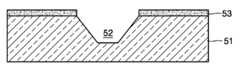
도 8a 내지 도 8f를 참조하면, 본 발명의 일 실시예에 따른 광부품 실장용 기판 제조방법은 기판(51)에 그루브(52)를 형성하는 단계와 기판 상에 포토리소그래피 공정에 의하여 스토퍼(59)를 형성하는 단계를 포함한다.8A to 8F, the method for manufacturing an optical component mounting substrate according to an embodiment of the present invention includes forming a
도 8a 내지 도 8d는 기판(51)를 식각하여 그루브(52)를 형성하는 공정을 설명하기 위한 도면으로, 순서대로 설명하면 다음과 같다.8A to 8D are diagrams for describing a process of forming the
준비된 기판(51) 상에 포토레지스트(53)를 도포하고, 그 상부에 그루브에 대응되는 패턴을 갖는 마스크(55)를 위치시키고, 노광 공정을 통하여 포토레지스트(53)의 일부를 감광시킨다(도 8a). 이후, 마스크(55)를 제거한 후 세 정 공정을 통하여 그루브에 대응되는 개구부(53a)를 형성한다(도 8b). 이어서, 비등방성 식각을 통하여(도 8c), 측벽이 경사진 그루브(52)를 형성한다(도 8d).The
도 8e와 도 8f는 스토퍼 형성공정의 일 실시예를 보인 도면으로, 순서대로 설명하면 다음과 같다.8E and 8F illustrate an embodiment of a stopper forming process, which will be described below in order.
그루브가 형성된 기판(51)의 상면에 빛에 감응하는 폴리머층(57)을 형성하고, 스토퍼에 대응되는 형상의 마스크(58)를 소정 위치에 마련한다(도 8e). 이어서, 상기 폴리머층(57)의 일부를 노광 및 세정을 통하여 제거한다(도 8f). 이에 따라, 제거 후 상기 기판(51) 및 그루브(52) 상에 존재하는 폴리머가 스토퍼(59)를 이룬다.A
도 9a 내지 도 9c는 도 8a 내지 도 8d에 도시된 그루브 형성 공정 이후에, 진행되는 스토퍼 형성공정의 다른 실시예를 보인 도면으로, 순서대로 설명하면 다음과 같다.9A to 9C illustrate another embodiment of the stopper forming process that is performed after the groove forming process illustrated in FIGS. 8A to 8D.
그루브가 형성된 기판(51)의 상면에 빛에 감응하는 폴리머층(65)을 형성하고, 스토퍼에 대응되는 형상의 마스크(63)를 소정 위치에 마련하고, 노광을 행한다(도 9a). 이어서, 마스크(63)와 스토퍼에 대응되는 부분의 폴리머층(65)을 세정을 통하여 제거하여 몰드(65)를 형성한다(도 9b). 이후, 상기 몰드(65)에 금속도금을 하여 스토퍼(67)를 형성하고, 몰드(65)를 제거하여 스토퍼를 완성한다.A
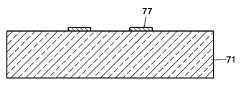
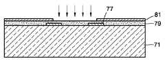
도 10a 내지 도 10g와, 도 11 및 도 12를 참조하면, 본 발명의 다른 실시예에 따른 광부품 실장용 기판 제조방법은 기판(71)에 포토리소그래피 공정에 의하여 스토퍼(77)를 형성하는 단계와, 스토퍼(77)가 형성된 기판을 식각하여 그루브(72) 를 형성하는 단계를 포함한다.Referring to FIGS. 10A to 10G and FIGS. 11 and 12, a method of manufacturing an optical component mounting substrate according to another exemplary embodiment may include forming a
도 10a 내지 도 10c 및, 도 11은 기판(71) 상에 스토퍼 형성공정의 일 실시예를 보인 도면으로, 순서대로 설명하면 다음과 같다.10A to 10C and FIG. 11 are views illustrating an embodiment of a stopper forming process on the
준비된 기판(51)의 상면에 빛에 감응하는 폴리머층(73)을 형성하고, 스토퍼에 대응되는 형상의 마스크(75)를 소정 위치에 마련하고, 노광을 행한다(도 10a). 이어서, 마스크(75)와 스토퍼에 대응되는 부분의 폴리머층(73)을 세정을 통하여 제거하여 몰드(73)를 형성한다(도 10b). 이후, 상기 몰드(73)의 개구부(73a)에 금속도금을 하여 스토퍼(77)를 형성하고, 몰드(73)를 제거하여 스토퍼를 완성한다(도 10c). 도 11은 도 10c의 공정 후의 광부품 실장용 기판을 보인 평면도로서, A-A'선 단면이 도 10c의 단면도이다.A
한편, 상기 스토퍼 형성공정의 다른 실시예는 도 8e 및 도 8f를 참조하여 설명된 스토퍼 형성공정과 실질적으로 동일하다. 즉, 기판 상면에 형성된 폴리머층의 일부를 노광한 후, 세정을 통하여 제거하고, 제거 후 기판 상에 존재하는 폴리머를 스토퍼로 이용한다. 한편, 그루브 형성 전에 스토퍼를 형성하는 점에서 구별된다.Meanwhile, another embodiment of the stopper forming process is substantially the same as the stopper forming process described with reference to FIGS. 8E and 8F. That is, a part of the polymer layer formed on the upper surface of the substrate is exposed and then removed by washing, and the polymer present on the substrate after the removal is used as a stopper. On the other hand, it distinguishes in the point which forms a stopper before groove formation.
도 10d 내지 도 10g 및, 도 12는 본 실시예에 따른 그루브 형성공정을 설명하기 위한 도면으로, 순서대로 설명하면 다음과 같다.10D to 10G and FIG. 12 are views for explaining a groove forming process according to the present embodiment, which will be described below in order.
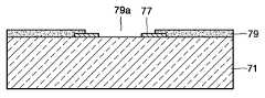
스토퍼(77)가 형성된 기판(71) 상에 포토레지스트(79)를 도포하고, 그 상부에 원통형 렌즈(도 7의 41)가 실장 될 그루브에 대응되는 패턴을 갖는 마스크(81)를 위치시킨 후, 노광한다(10d). 이어서, 세정공정을 통하여 마스크(81)와 포토레지스트의 상기 그루브에 대응되는 부분을 제거한다(도 10e).After the
이후, 식각공정을 통하여 경사진 측벽을 갖는 광부품 실장용 그루브를 형성한다(도 10f). 여기서, 기판은 <100> 결정방향을 갖는 실리콘 웨이퍼 등으로 된 것으로, 비등방 식각을 통하여 형성된다. 이 때, 스토퍼(77) 일 부분의 하부는 볼록 마스크(convex mask) 효과에 의해 식각된다.Thereafter, an groove for mounting an optical component having an inclined sidewall is formed through an etching process (FIG. 10F). Here, the substrate is made of a silicon wafer or the like having a <100> crystallographic direction, and is formed through anisotropic etching. At this time, the lower portion of the portion of the
마지막으로 포토레지스트(79)를 제거함으로써, 스토퍼(77) 제조공정 및 글루브 형성공정이 완료된다(도 10g). 도 12는 도 10g의 공정 후의 광부품 실장용 기판을 보인 평면도로서, 그 B-B'선 단면이 도 10g의 단면도이다.Finally, by removing the
상기한 바와 같이, 구성된 본 발명에 따른 광부품 실장용 기판 및 그 제조방법은 z축 방향으로의 실장 위치를 가이드하는 스토퍼를 형성함으로써, 원통형 렌즈를 장착하는 경우에도 x축 방향 뿐만 아니라 z축 방향으로의 수동 어라인먼트를 용이하게 할 수 있다. 또한, 포토리소그래피 공정을 통하여 스토퍼를 형성함으로써, z축 방향으로의 광부품의 조립공차를 ±5㎛ 이내를 유지할 수 있다.As described above, the optical component mounting substrate and the manufacturing method thereof according to the present invention have a stopper for guiding the mounting position in the z-axis direction, so that not only the x-axis direction but also the z-axis direction when the cylindrical lens is mounted Manual alignment to the furnace can be facilitated. In addition, by forming the stopper through the photolithography step, the assembly tolerance of the optical component in the z-axis direction can be maintained within ± 5 μm.
따라서, 상기한 기판을 이용하는 경우, 광스폿의 품질이 향상되어 높은 광결합 효율이 요구되는 광전 디바이스 모듈의 제작이 가능하다는 이점이 있다.Therefore, in the case of using the above-described substrate, there is an advantage that the quality of the light spot can be improved, and thus the production of the optoelectronic device module requiring high optical coupling efficiency is possible.
Claims (11)
Translated fromKoreanPriority Applications (2)
| Application Number | Priority Date | Filing Date | Title |
|---|---|---|---|
| KR1020020059779AKR100624405B1 (en) | 2002-10-01 | 2002-10-01 | Optical component mounting board and its manufacturing method |
| US10/372,191US6954578B2 (en) | 2002-10-01 | 2003-02-25 | Substrate for mounting optical component and method of manufacturing the same |
Applications Claiming Priority (1)
| Application Number | Priority Date | Filing Date | Title |
|---|---|---|---|
| KR1020020059779AKR100624405B1 (en) | 2002-10-01 | 2002-10-01 | Optical component mounting board and its manufacturing method |
Publications (2)
| Publication Number | Publication Date |
|---|---|
| KR20040029494A KR20040029494A (en) | 2004-04-08 |
| KR100624405B1true KR100624405B1 (en) | 2006-09-18 |
Family
ID=32026112
Family Applications (1)
| Application Number | Title | Priority Date | Filing Date |
|---|---|---|---|
| KR1020020059779AExpired - Fee RelatedKR100624405B1 (en) | 2002-10-01 | 2002-10-01 | Optical component mounting board and its manufacturing method |
Country Status (2)
| Country | Link |
|---|---|
| US (1) | US6954578B2 (en) |
| KR (1) | KR100624405B1 (en) |
Families Citing this family (33)
| Publication number | Priority date | Publication date | Assignee | Title |
|---|---|---|---|---|
| IL165212A (en) | 2004-11-15 | 2012-05-31 | Elbit Systems Electro Optics Elop Ltd | Device for scanning light |
| WO2007043036A1 (en) | 2005-10-11 | 2007-04-19 | Prime Sense Ltd. | Method and system for object reconstruction |
| US9330324B2 (en) | 2005-10-11 | 2016-05-03 | Apple Inc. | Error compensation in three-dimensional mapping |
| KR101331543B1 (en) | 2006-03-14 | 2013-11-20 | 프라임센스 엘티디. | Three-dimensional sensing using speckle patterns |
| US7900336B2 (en)* | 2006-04-14 | 2011-03-08 | Massachusetts Institute Of Technology | Precise hand-assembly of microfabricated components |
| DE102006032047A1 (en)* | 2006-07-10 | 2008-01-24 | Schott Ag | Optoelectronic component e.g. image signal-detecting component, manufacturing method for e.g. digital fixed image camera, involves positioning components either one by one or in groups relative to position of associated components of wafer |
| US8493496B2 (en) | 2007-04-02 | 2013-07-23 | Primesense Ltd. | Depth mapping using projected patterns |
| US8494252B2 (en) | 2007-06-19 | 2013-07-23 | Primesense Ltd. | Depth mapping using optical elements having non-uniform focal characteristics |
| US8456517B2 (en) | 2008-07-09 | 2013-06-04 | Primesense Ltd. | Integrated processor for 3D mapping |
| US8786682B2 (en)* | 2009-03-05 | 2014-07-22 | Primesense Ltd. | Reference image techniques for three-dimensional sensing |
| US8717417B2 (en)* | 2009-04-16 | 2014-05-06 | Primesense Ltd. | Three-dimensional mapping and imaging |
| WO2011013079A1 (en)* | 2009-07-30 | 2011-02-03 | Primesense Ltd. | Depth mapping based on pattern matching and stereoscopic information |
| US8830227B2 (en)* | 2009-12-06 | 2014-09-09 | Primesense Ltd. | Depth-based gain control |
| US9825425B2 (en) | 2013-06-19 | 2017-11-21 | Apple Inc. | Integrated structured-light projector comprising light-emitting elements on a substrate |
| US8982182B2 (en)* | 2010-03-01 | 2015-03-17 | Apple Inc. | Non-uniform spatial resource allocation for depth mapping |
| WO2012020380A1 (en) | 2010-08-11 | 2012-02-16 | Primesense Ltd. | Scanning projectors and image capture modules for 3d mapping |
| EP2643659B1 (en) | 2010-11-19 | 2019-12-25 | Apple Inc. | Depth mapping using time-coded illumination |
| US9167138B2 (en) | 2010-12-06 | 2015-10-20 | Apple Inc. | Pattern projection and imaging using lens arrays |
| US9030528B2 (en) | 2011-04-04 | 2015-05-12 | Apple Inc. | Multi-zone imaging sensor and lens array |
| CN104160240B (en) | 2012-02-15 | 2017-02-22 | 苹果公司 | Scanning depth engine |
| US9329080B2 (en) | 2012-02-15 | 2016-05-03 | Aplle Inc. | Modular optics for scanning engine having beam combining optics with a prism intercepted by both beam axis and collection axis |
| EP2828833B1 (en) | 2012-03-22 | 2017-03-08 | Apple Inc. | Gimbaled scanning mirror array |
| WO2014016794A1 (en) | 2012-07-26 | 2014-01-30 | Primesense Ltd. | Dual-axis scanning mirror |
| WO2014064606A1 (en) | 2012-10-23 | 2014-05-01 | Primesense Ltd. | Production of micro-mechanical devices |
| US9835853B1 (en) | 2014-11-26 | 2017-12-05 | Apple Inc. | MEMS scanner with mirrors of different sizes |
| US9784838B1 (en) | 2014-11-26 | 2017-10-10 | Apple Inc. | Compact scanner with gimbaled optics |
| US9798135B2 (en) | 2015-02-16 | 2017-10-24 | Apple Inc. | Hybrid MEMS scanning module |
| US9525863B2 (en) | 2015-04-29 | 2016-12-20 | Apple Inc. | Time-of-flight depth mapping with flexible scan pattern |
| US9703096B2 (en) | 2015-09-30 | 2017-07-11 | Apple Inc. | Asymmetric MEMS mirror assembly |
| US9897801B2 (en) | 2015-09-30 | 2018-02-20 | Apple Inc. | Multi-hinge mirror assembly |
| US10488652B2 (en) | 2016-09-21 | 2019-11-26 | Apple Inc. | Prism-based scanner |
| US10153614B1 (en) | 2017-08-31 | 2018-12-11 | Apple Inc. | Creating arbitrary patterns on a 2-D uniform grid VCSEL array |
| WO2021034371A1 (en) | 2019-08-18 | 2021-02-25 | Apple Inc. | Force-balanced micromirror with electromagnetic actuation |
Citations (5)
| Publication number | Priority date | Publication date | Assignee | Title |
|---|---|---|---|---|
| US5557695A (en)* | 1994-05-12 | 1996-09-17 | Fujitsu Limited | Waveguide-optical fiber connection structure and waveguide-optical fiber connection method |
| JPH09145958A (en)* | 1995-11-22 | 1997-06-06 | Fujikura Ltd | Optical fiber connection |
| US5793914A (en)* | 1995-08-21 | 1998-08-11 | Nec Corporation | Optical module & method for manufacturing the same |
| US5961849A (en)* | 1995-01-25 | 1999-10-05 | Cambridge Consultants Ltd. | Miniature mounting device and method |
| US20020186923A1 (en)* | 2001-06-12 | 2002-12-12 | Ynh-Sheng Lin | Method for fabricating integrated micro spherical lens for optical fiber switch and the device made therefrom |
Family Cites Families (7)
| Publication number | Priority date | Publication date | Assignee | Title |
|---|---|---|---|---|
| US4897711A (en)* | 1988-03-03 | 1990-01-30 | American Telephone And Telegraph Company | Subassembly for optoelectronic devices |
| US5017263A (en)* | 1988-12-23 | 1991-05-21 | At&T Bell Laboratories | Optoelectronic device package method |
| US6071017A (en)* | 1996-01-18 | 2000-06-06 | Methode Electronics, Inc. | Optical package with alignment means and method of assembling an optical package |
| US6123465A (en)* | 1996-03-21 | 2000-09-26 | Nippon Sheet Glass Company Ltd | Optical module |
| US5848211A (en)* | 1996-08-28 | 1998-12-08 | Hewlett-Packard Company | Photonics module having its components mounted on a single mounting member |
| JP2003098407A (en)* | 2001-09-26 | 2003-04-03 | Nec Compound Semiconductor Devices Ltd | Semiconductor optical coupling device |
| EP1327899A1 (en)* | 2002-01-07 | 2003-07-16 | Alcatel | A method for manufacturing an optical module and an optical module |
- 2002
- 2002-10-01KRKR1020020059779Apatent/KR100624405B1/ennot_activeExpired - Fee Related
- 2003
- 2003-02-25USUS10/372,191patent/US6954578B2/ennot_activeExpired - Lifetime
Patent Citations (5)
| Publication number | Priority date | Publication date | Assignee | Title |
|---|---|---|---|---|
| US5557695A (en)* | 1994-05-12 | 1996-09-17 | Fujitsu Limited | Waveguide-optical fiber connection structure and waveguide-optical fiber connection method |
| US5961849A (en)* | 1995-01-25 | 1999-10-05 | Cambridge Consultants Ltd. | Miniature mounting device and method |
| US5793914A (en)* | 1995-08-21 | 1998-08-11 | Nec Corporation | Optical module & method for manufacturing the same |
| JPH09145958A (en)* | 1995-11-22 | 1997-06-06 | Fujikura Ltd | Optical fiber connection |
| US20020186923A1 (en)* | 2001-06-12 | 2002-12-12 | Ynh-Sheng Lin | Method for fabricating integrated micro spherical lens for optical fiber switch and the device made therefrom |
Also Published As
| Publication number | Publication date |
|---|---|
| KR20040029494A (en) | 2004-04-08 |
| US20040063235A1 (en) | 2004-04-01 |
| US6954578B2 (en) | 2005-10-11 |
Similar Documents
| Publication | Publication Date | Title |
|---|---|---|
| KR100624405B1 (en) | Optical component mounting board and its manufacturing method | |
| US11378751B2 (en) | Laser patterned adapters with waveguides and etched connectors for low cost alignment of optics to chips | |
| JPH07117631B2 (en) | Automatic matching optical parts | |
| US5633968A (en) | Face-lock interconnection means for optical fibers and other optical components and manufacturing methods of the same | |
| US6811853B1 (en) | Single mask lithographic process for patterning multiple types of surface features | |
| EP1258769B1 (en) | Optical module and method for manufacturing the same | |
| US6870990B2 (en) | Optical device, optical device mounting method, and optical module | |
| US5935451A (en) | Fabrication of etched features | |
| US5980119A (en) | Single-crystal component to be applied to optical module and its fabrication method | |
| EP1184696A1 (en) | Self-aligning optical component assembly on a common substrate | |
| US6934449B2 (en) | Optical device permitting passive alignment of lens element | |
| JP2005292379A (en) | Optical coupling device and manufacturing method therefor | |
| JP2010175592A (en) | Optical element | |
| JP2005109055A (en) | Optical semiconductor device and its manufacturing method | |
| CA2324675C (en) | A substrate for mounting an optical component, a method for producing the same, and an optical module using the same | |
| US6523804B1 (en) | Metallic building element for optoelectronics | |
| KR100396742B1 (en) | Optical integrated circuit device having protrusion, fabrication method of the same and module of optical communication transmission and receiving apparatus using the same | |
| JPH09159866A (en) | Substrate for optical coupler, optical coupler and their production | |
| KR19990079489A (en) | Silicon wafer fabrication method and mounting structure of silicon wafer and photodiode chip | |
| KR20060009693A (en) | Polymer optical waveguide formation method for passive alignment with optical fiber in optical module | |
| KR100407954B1 (en) | Fabrication Method for Optical Bench of Optical Device subassemblies | |
| KR100506208B1 (en) | Method for fabricating lens on planar lightwave circuit plaform | |
| WO2004038471A1 (en) | An optical board with electrical and optical wiring layers and a method of its production | |
| JPH10170773A (en) | Method of manufacturing optical device mounting substrate and optical module | |
| JPH11337775A (en) | Packaging substrate, production of packaging substrate and production of optical module |
Legal Events
| Date | Code | Title | Description |
|---|---|---|---|
| A201 | Request for examination | ||
| PA0109 | Patent application | St.27 status event code:A-0-1-A10-A12-nap-PA0109 | |
| PA0201 | Request for examination | St.27 status event code:A-1-2-D10-D11-exm-PA0201 | |
| R18-X000 | Changes to party contact information recorded | St.27 status event code:A-3-3-R10-R18-oth-X000 | |
| R18-X000 | Changes to party contact information recorded | St.27 status event code:A-3-3-R10-R18-oth-X000 | |
| R18-X000 | Changes to party contact information recorded | St.27 status event code:A-3-3-R10-R18-oth-X000 | |
| D13-X000 | Search requested | St.27 status event code:A-1-2-D10-D13-srh-X000 | |
| PG1501 | Laying open of application | St.27 status event code:A-1-1-Q10-Q12-nap-PG1501 | |
| D14-X000 | Search report completed | St.27 status event code:A-1-2-D10-D14-srh-X000 | |
| E902 | Notification of reason for refusal | ||
| PE0902 | Notice of grounds for rejection | St.27 status event code:A-1-2-D10-D21-exm-PE0902 | |
| AMND | Amendment | ||
| E13-X000 | Pre-grant limitation requested | St.27 status event code:A-2-3-E10-E13-lim-X000 | |
| P11-X000 | Amendment of application requested | St.27 status event code:A-2-2-P10-P11-nap-X000 | |
| P13-X000 | Application amended | St.27 status event code:A-2-2-P10-P13-nap-X000 | |
| E601 | Decision to refuse application | ||
| PE0601 | Decision on rejection of patent | St.27 status event code:N-2-6-B10-B15-exm-PE0601 | |
| J201 | Request for trial against refusal decision | ||
| PJ0201 | Trial against decision of rejection | St.27 status event code:A-3-3-V10-V11-apl-PJ0201 | |
| AMND | Amendment | ||
| P11-X000 | Amendment of application requested | St.27 status event code:A-2-2-P10-P11-nap-X000 | |
| PB0901 | Examination by re-examination before a trial | St.27 status event code:A-6-3-E10-E12-rex-PB0901 | |
| E801 | Decision on dismissal of amendment | ||
| PE0801 | Dismissal of amendment | St.27 status event code:A-2-2-P10-P12-nap-PE0801 | |
| B601 | Maintenance of original decision after re-examination before a trial | ||
| PB0601 | Maintenance of original decision after re-examination before a trial | St.27 status event code:N-3-6-B10-B17-rex-PB0601 | |
| R17-X000 | Change to representative recorded | St.27 status event code:A-3-3-R10-R17-oth-X000 | |
| PN2301 | Change of applicant | St.27 status event code:A-3-3-R10-R13-asn-PN2301 St.27 status event code:A-3-3-R10-R11-asn-PN2301 | |
| PN2301 | Change of applicant | St.27 status event code:A-3-3-R10-R13-asn-PN2301 St.27 status event code:A-3-3-R10-R11-asn-PN2301 | |
| J301 | Trial decision | Free format text:TRIAL DECISION FOR APPEAL AGAINST DECISION TO DECLINE REFUSAL REQUESTED 20050330 Effective date:20060623 | |
| PJ1301 | Trial decision | St.27 status event code:A-3-3-V10-V15-crt-PJ1301 Decision date:20060623 Appeal event data comment text:Appeal Kind Category : Appeal against decision to decline refusal, Appeal Ground Text : 2002 59779 Appeal request date:20050330 Appellate body name:Patent Examination Board Decision authority category:Office appeal board Decision identifier:2005101001953 | |
| PS0901 | Examination by remand of revocation | St.27 status event code:A-6-3-E10-E12-rex-PS0901 | |
| S901 | Examination by remand of revocation | ||
| GRNO | Decision to grant (after opposition) | ||
| PS0701 | Decision of registration after remand of revocation | St.27 status event code:A-3-4-F10-F13-rex-PS0701 | |
| GRNT | Written decision to grant | ||
| PR0701 | Registration of establishment | St.27 status event code:A-2-4-F10-F11-exm-PR0701 | |
| PR1002 | Payment of registration fee | St.27 status event code:A-2-2-U10-U11-oth-PR1002 Fee payment year number:1 | |
| PG1601 | Publication of registration | St.27 status event code:A-4-4-Q10-Q13-nap-PG1601 | |
| PR1001 | Payment of annual fee | St.27 status event code:A-4-4-U10-U11-oth-PR1001 Fee payment year number:4 | |
| PR1001 | Payment of annual fee | St.27 status event code:A-4-4-U10-U11-oth-PR1001 Fee payment year number:5 | |
| PR1001 | Payment of annual fee | St.27 status event code:A-4-4-U10-U11-oth-PR1001 Fee payment year number:6 | |
| R18-X000 | Changes to party contact information recorded | St.27 status event code:A-5-5-R10-R18-oth-X000 | |
| FPAY | Annual fee payment | Payment date:20120814 Year of fee payment:7 | |
| PR1001 | Payment of annual fee | St.27 status event code:A-4-4-U10-U11-oth-PR1001 Fee payment year number:7 | |
| FPAY | Annual fee payment | Payment date:20130822 Year of fee payment:8 | |
| PR1001 | Payment of annual fee | St.27 status event code:A-4-4-U10-U11-oth-PR1001 Fee payment year number:8 | |
| FPAY | Annual fee payment | Payment date:20140822 Year of fee payment:9 | |
| PR1001 | Payment of annual fee | St.27 status event code:A-4-4-U10-U11-oth-PR1001 Fee payment year number:9 | |
| LAPS | Lapse due to unpaid annual fee | ||
| PC1903 | Unpaid annual fee | St.27 status event code:A-4-4-U10-U13-oth-PC1903 Not in force date:20150909 Payment event data comment text:Termination Category : DEFAULT_OF_REGISTRATION_FEE | |
| PC1903 | Unpaid annual fee | St.27 status event code:N-4-6-H10-H13-oth-PC1903 Ip right cessation event data comment text:Termination Category : DEFAULT_OF_REGISTRATION_FEE Not in force date:20150909 |