KR100618252B1 - Image display apparatus and its method of operation - Google Patents
Image display apparatus and its method of operationDownload PDFInfo
- Publication number
- KR100618252B1 KR100618252B1KR1020000038850AKR20000038850AKR100618252B1KR 100618252 B1KR100618252 B1KR 100618252B1KR 1020000038850 AKR1020000038850 AKR 1020000038850AKR 20000038850 AKR20000038850 AKR 20000038850AKR 100618252 B1KR100618252 B1KR 100618252B1
- Authority
- KR
- South Korea
- Prior art keywords
- common source
- line
- source line
- correction data
- data
- Prior art date
- Legal status (The legal status is an assumption and is not a legal conclusion. Google has not performed a legal analysis and makes no representation as to the accuracy of the status listed.)
- Expired - Lifetime
Links
- 238000000034methodMethods0.000titleclaimsdescription19
- 239000011159matrix materialSubstances0.000claimsabstractdescription39
- 230000004913activationEffects0.000claimsabstractdescription3
- 230000009849deactivationEffects0.000claimsabstractdescription3
- 238000012937correctionMethods0.000claimsdescription220
- 230000015654memoryEffects0.000claimsdescription135
- 238000004891communicationMethods0.000claimsdescription36
- 230000008859changeEffects0.000claimsdescription8
- 230000005855radiationEffects0.000claims2
- 230000003213activating effectEffects0.000claims1
- 239000003086colorantSubstances0.000claims1
- 238000010586diagramMethods0.000description18
- 102100021568B-cell scaffold protein with ankyrin repeatsHuman genes0.000description9
- 101000971155Homo sapiens B-cell scaffold protein with ankyrin repeatsProteins0.000description9
- 238000012546transferMethods0.000description8
- 230000000694effectsEffects0.000description6
- 230000002093peripheral effectEffects0.000description3
- 230000004044responseEffects0.000description3
- 238000009825accumulationMethods0.000description2
- 230000006870functionEffects0.000description2
- 238000011835investigationMethods0.000description2
- 230000000717retained effectEffects0.000description2
- 235000012431wafersNutrition0.000description2
- 230000005540biological transmissionEffects0.000description1
- 230000003247decreasing effectEffects0.000description1
- 238000007599dischargingMethods0.000description1
- 238000005516engineering processMethods0.000description1
- 238000007667floatingMethods0.000description1
- 238000005286illuminationMethods0.000description1
- 238000004519manufacturing processMethods0.000description1
- 238000012986modificationMethods0.000description1
- 230000004048modificationEffects0.000description1
- 238000012545processingMethods0.000description1
- 239000004065semiconductorSubstances0.000description1
- 230000001360synchronised effectEffects0.000description1
Images


Classifications
- G—PHYSICS
- G09—EDUCATION; CRYPTOGRAPHY; DISPLAY; ADVERTISING; SEALS
- G09G—ARRANGEMENTS OR CIRCUITS FOR CONTROL OF INDICATING DEVICES USING STATIC MEANS TO PRESENT VARIABLE INFORMATION
- G09G3/00—Control arrangements or circuits, of interest only in connection with visual indicators other than cathode-ray tubes
- G09G3/20—Control arrangements or circuits, of interest only in connection with visual indicators other than cathode-ray tubes for presentation of an assembly of a number of characters, e.g. a page, by composing the assembly by combination of individual elements arranged in a matrix no fixed position being assigned to or needed to be assigned to the individual characters or partial characters
- G09G3/22—Control arrangements or circuits, of interest only in connection with visual indicators other than cathode-ray tubes for presentation of an assembly of a number of characters, e.g. a page, by composing the assembly by combination of individual elements arranged in a matrix no fixed position being assigned to or needed to be assigned to the individual characters or partial characters using controlled light sources
- G09G3/30—Control arrangements or circuits, of interest only in connection with visual indicators other than cathode-ray tubes for presentation of an assembly of a number of characters, e.g. a page, by composing the assembly by combination of individual elements arranged in a matrix no fixed position being assigned to or needed to be assigned to the individual characters or partial characters using controlled light sources using electroluminescent panels
- G09G3/32—Control arrangements or circuits, of interest only in connection with visual indicators other than cathode-ray tubes for presentation of an assembly of a number of characters, e.g. a page, by composing the assembly by combination of individual elements arranged in a matrix no fixed position being assigned to or needed to be assigned to the individual characters or partial characters using controlled light sources using electroluminescent panels semiconductive, e.g. using light-emitting diodes [LED]
- G09G3/3208—Control arrangements or circuits, of interest only in connection with visual indicators other than cathode-ray tubes for presentation of an assembly of a number of characters, e.g. a page, by composing the assembly by combination of individual elements arranged in a matrix no fixed position being assigned to or needed to be assigned to the individual characters or partial characters using controlled light sources using electroluminescent panels semiconductive, e.g. using light-emitting diodes [LED] organic, e.g. using organic light-emitting diodes [OLED]
- G09G3/3216—Control arrangements or circuits, of interest only in connection with visual indicators other than cathode-ray tubes for presentation of an assembly of a number of characters, e.g. a page, by composing the assembly by combination of individual elements arranged in a matrix no fixed position being assigned to or needed to be assigned to the individual characters or partial characters using controlled light sources using electroluminescent panels semiconductive, e.g. using light-emitting diodes [LED] organic, e.g. using organic light-emitting diodes [OLED] using a passive matrix
- G—PHYSICS
- G09—EDUCATION; CRYPTOGRAPHY; DISPLAY; ADVERTISING; SEALS
- G09G—ARRANGEMENTS OR CIRCUITS FOR CONTROL OF INDICATING DEVICES USING STATIC MEANS TO PRESENT VARIABLE INFORMATION
- G09G3/00—Control arrangements or circuits, of interest only in connection with visual indicators other than cathode-ray tubes
- G09G3/20—Control arrangements or circuits, of interest only in connection with visual indicators other than cathode-ray tubes for presentation of an assembly of a number of characters, e.g. a page, by composing the assembly by combination of individual elements arranged in a matrix no fixed position being assigned to or needed to be assigned to the individual characters or partial characters
- G09G3/22—Control arrangements or circuits, of interest only in connection with visual indicators other than cathode-ray tubes for presentation of an assembly of a number of characters, e.g. a page, by composing the assembly by combination of individual elements arranged in a matrix no fixed position being assigned to or needed to be assigned to the individual characters or partial characters using controlled light sources
- G09G3/30—Control arrangements or circuits, of interest only in connection with visual indicators other than cathode-ray tubes for presentation of an assembly of a number of characters, e.g. a page, by composing the assembly by combination of individual elements arranged in a matrix no fixed position being assigned to or needed to be assigned to the individual characters or partial characters using controlled light sources using electroluminescent panels
- G09G3/32—Control arrangements or circuits, of interest only in connection with visual indicators other than cathode-ray tubes for presentation of an assembly of a number of characters, e.g. a page, by composing the assembly by combination of individual elements arranged in a matrix no fixed position being assigned to or needed to be assigned to the individual characters or partial characters using controlled light sources using electroluminescent panels semiconductive, e.g. using light-emitting diodes [LED]
- G09G3/3208—Control arrangements or circuits, of interest only in connection with visual indicators other than cathode-ray tubes for presentation of an assembly of a number of characters, e.g. a page, by composing the assembly by combination of individual elements arranged in a matrix no fixed position being assigned to or needed to be assigned to the individual characters or partial characters using controlled light sources using electroluminescent panels semiconductive, e.g. using light-emitting diodes [LED] organic, e.g. using organic light-emitting diodes [OLED]
- G09G3/3275—Details of drivers for data electrodes
- G—PHYSICS
- G09—EDUCATION; CRYPTOGRAPHY; DISPLAY; ADVERTISING; SEALS
- G09G—ARRANGEMENTS OR CIRCUITS FOR CONTROL OF INDICATING DEVICES USING STATIC MEANS TO PRESENT VARIABLE INFORMATION
- G09G2300/00—Aspects of the constitution of display devices
- G09G2300/06—Passive matrix structure, i.e. with direct application of both column and row voltages to the light emitting or modulating elements, other than LCD or OLED
- G—PHYSICS
- G09—EDUCATION; CRYPTOGRAPHY; DISPLAY; ADVERTISING; SEALS
- G09G—ARRANGEMENTS OR CIRCUITS FOR CONTROL OF INDICATING DEVICES USING STATIC MEANS TO PRESENT VARIABLE INFORMATION
- G09G2310/00—Command of the display device
- G09G2310/02—Addressing, scanning or driving the display screen or processing steps related thereto
- G09G2310/0243—Details of the generation of driving signals
- G09G2310/0251—Precharge or discharge of pixel before applying new pixel voltage
- G—PHYSICS
- G09—EDUCATION; CRYPTOGRAPHY; DISPLAY; ADVERTISING; SEALS
- G09G—ARRANGEMENTS OR CIRCUITS FOR CONTROL OF INDICATING DEVICES USING STATIC MEANS TO PRESENT VARIABLE INFORMATION
- G09G2310/00—Command of the display device
- G09G2310/02—Addressing, scanning or driving the display screen or processing steps related thereto
- G09G2310/0264—Details of driving circuits
- G09G2310/027—Details of drivers for data electrodes, the drivers handling digital grey scale data, e.g. use of D/A converters
- G—PHYSICS
- G09—EDUCATION; CRYPTOGRAPHY; DISPLAY; ADVERTISING; SEALS
- G09G—ARRANGEMENTS OR CIRCUITS FOR CONTROL OF INDICATING DEVICES USING STATIC MEANS TO PRESENT VARIABLE INFORMATION
- G09G2310/00—Command of the display device
- G09G2310/06—Details of flat display driving waveforms
- G09G2310/061—Details of flat display driving waveforms for resetting or blanking
- G—PHYSICS
- G09—EDUCATION; CRYPTOGRAPHY; DISPLAY; ADVERTISING; SEALS
- G09G—ARRANGEMENTS OR CIRCUITS FOR CONTROL OF INDICATING DEVICES USING STATIC MEANS TO PRESENT VARIABLE INFORMATION
- G09G2320/00—Control of display operating conditions
- G09G2320/02—Improving the quality of display appearance
- G09G2320/0285—Improving the quality of display appearance using tables for spatial correction of display data
- G—PHYSICS
- G09—EDUCATION; CRYPTOGRAPHY; DISPLAY; ADVERTISING; SEALS
- G09G—ARRANGEMENTS OR CIRCUITS FOR CONTROL OF INDICATING DEVICES USING STATIC MEANS TO PRESENT VARIABLE INFORMATION
- G09G2320/00—Control of display operating conditions
- G09G2320/04—Maintaining the quality of display appearance
- G09G2320/043—Preventing or counteracting the effects of ageing
- G—PHYSICS
- G09—EDUCATION; CRYPTOGRAPHY; DISPLAY; ADVERTISING; SEALS
- G09G—ARRANGEMENTS OR CIRCUITS FOR CONTROL OF INDICATING DEVICES USING STATIC MEANS TO PRESENT VARIABLE INFORMATION
- G09G2370/00—Aspects of data communication
- G09G2370/04—Exchange of auxiliary data, i.e. other than image data, between monitor and graphics controller
- G—PHYSICS
- G09—EDUCATION; CRYPTOGRAPHY; DISPLAY; ADVERTISING; SEALS
- G09G—ARRANGEMENTS OR CIRCUITS FOR CONTROL OF INDICATING DEVICES USING STATIC MEANS TO PRESENT VARIABLE INFORMATION
- G09G3/00—Control arrangements or circuits, of interest only in connection with visual indicators other than cathode-ray tubes
- G09G3/20—Control arrangements or circuits, of interest only in connection with visual indicators other than cathode-ray tubes for presentation of an assembly of a number of characters, e.g. a page, by composing the assembly by combination of individual elements arranged in a matrix no fixed position being assigned to or needed to be assigned to the individual characters or partial characters
- G09G3/22—Control arrangements or circuits, of interest only in connection with visual indicators other than cathode-ray tubes for presentation of an assembly of a number of characters, e.g. a page, by composing the assembly by combination of individual elements arranged in a matrix no fixed position being assigned to or needed to be assigned to the individual characters or partial characters using controlled light sources
- G09G3/30—Control arrangements or circuits, of interest only in connection with visual indicators other than cathode-ray tubes for presentation of an assembly of a number of characters, e.g. a page, by composing the assembly by combination of individual elements arranged in a matrix no fixed position being assigned to or needed to be assigned to the individual characters or partial characters using controlled light sources using electroluminescent panels
- G09G3/32—Control arrangements or circuits, of interest only in connection with visual indicators other than cathode-ray tubes for presentation of an assembly of a number of characters, e.g. a page, by composing the assembly by combination of individual elements arranged in a matrix no fixed position being assigned to or needed to be assigned to the individual characters or partial characters using controlled light sources using electroluminescent panels semiconductive, e.g. using light-emitting diodes [LED]
- G09G3/3208—Control arrangements or circuits, of interest only in connection with visual indicators other than cathode-ray tubes for presentation of an assembly of a number of characters, e.g. a page, by composing the assembly by combination of individual elements arranged in a matrix no fixed position being assigned to or needed to be assigned to the individual characters or partial characters using controlled light sources using electroluminescent panels semiconductive, e.g. using light-emitting diodes [LED] organic, e.g. using organic light-emitting diodes [OLED]
- G09G3/3275—Details of drivers for data electrodes
- G09G3/3283—Details of drivers for data electrodes in which the data driver supplies a variable data current for setting the current through, or the voltage across, the light-emitting elements
Landscapes
- Engineering & Computer Science (AREA)
- Physics & Mathematics (AREA)
- Computer Hardware Design (AREA)
- General Physics & Mathematics (AREA)
- Theoretical Computer Science (AREA)
- Control Of Indicators Other Than Cathode Ray Tubes (AREA)
- Control Of El Displays (AREA)
Abstract
Translated fromKoreanDescription
Translated fromKorean도 1은 본 발명의 한 실시예의 화상 표시 장치의 구조적 포맷을 도시한 개념도,1 is a conceptual diagram showing the structural format of an image display device of an embodiment of the present invention;
도 2는 도 1에 도시한 화상 표시 장치의 특정 예를 도시한 블록도,FIG. 2 is a block diagram showing a specific example of the image display device shown in FIG. 1;
도 3은 화상 표시 장치의 다른 특정 예를 도시한 블록도,3 is a block diagram showing another specific example of an image display device;
도 4는 도 3에 도시한 공통 소스 드라이버 및 스위칭 회로 제어의 타이밍도,4 is a timing diagram of a common source driver and switching circuit control shown in FIG. 3;
도 5는 본 발명의 다른 실시예의 화상 표시 장치의 구조적 포맷을 도시한 개념도,5 is a conceptual diagram showing the structural format of an image display device of another embodiment of the present invention;
도 6은 도 5에 도시한 화상 표시 장치의 특정 예를 도시한 블록도,6 is a block diagram showing a specific example of the image display device shown in FIG. 5;
도 7은 도 6의 특정 실시예에서 전기적으로 소거가능하고 프로그램가능한 ROM(EEPROM) 및 직렬 통신 인터페이스의 상세한 구조를 도시한 블록도,7 is a block diagram illustrating the detailed structure of an electrically erasable and programmable ROM (EEPROM) and a serial communication interface in the particular embodiment of FIG. 6;
도 8은 본 발명의 다른 실시예의 화상 표시 장치의 구조적 포맷을 도시한 개념도,8 is a conceptual diagram showing the structural format of an image display device of another embodiment of the present invention;
도 9는 도 8에 도시한 화상 표시 장치의 특정 예를 도시한 블록도,9 is a block diagram showing a specific example of the image display device shown in FIG. 8;
도 10은 도 9에 도시한 화상 표시 장치에서의 보정 데이터 전송 타이밍을 도시한 타이밍도,10 is a timing diagram showing a correction data transfer timing in the image display device shown in FIG. 9;
도 11은 도 9에 도시한 화상 표시 장치에서의 제어 라인 수와 ROM 독출 개시 어드레스 사이의 관계를 도시한 개략도,11 is a schematic diagram showing the relationship between the number of control lines and the ROM read start address in the image display device shown in FIG. 9;
도 12는 관련 분야 화상 표시 장치의 회로 구조를 도시한 블록도이다.12 is a block diagram showing a circuit structure of a related field image display device.
<도면의 주요부분에 대한 부호의 설명><Description of the symbols for the main parts of the drawings>
1: 전류 소스 스위칭 회로 2: 스위칭 회로부1: current source switching circuit 2: switching circuit section
3: 정전류 제어 회로부4: 발광 다이오드(LED)3: constant current control circuit portion 4: light emitting diode (LED)
5: 공통 소스 라인 6: 전류 라인5: common source line 6: current line
10: 도트 매트릭스 11: 디코더10: dot matrix 11: decoder
12: 공통 소스 드라이버 13: 스위칭 디코더 회로12: common source driver 13: switching decoder circuit
20: 버퍼 메모리부21: 표시부20: buffer memory section 21: display section
22: 수직 드라이버부23: 수평 드라이버부22: vertical driver part 23: horizontal driver part
24: 화상 데이터 보정부25: 제어부24: image data correction unit 25: control unit
26: 보정 데이터 메모리부27: 화상 데이터 입력부26: correction data memory unit 27: image data input unit
28: 통신 제어부31: 시프트 레지스터28: communication control unit 31: shift register
32: 메모리 회로33: 카운터32: memory circuit 33: counter
34: 데이터 비교기35: 정전류 드라이버부34: data comparator 35: constant current driver
41: LED 도트 매트릭스42: 공통 드라이버41: LED dot matrix 42: common driver
43: LED 드라이버 IC의 드라이버부44: LED 드라이버 IC43: driver portion of the LED driver IC 44: LED driver IC
45: 제어부 46: EEPROM45: control unit 46: EEPROM
47: 명령 제어부48:직렬 통신 인터페이스47: command control unit 48: serial communication interface
49: 보정 회로401: 레지스터49: correction circuit 401: register
402: 시프트 레지스터402: shift register
본 발명은, 매트릭스 표시 패널로 배열된 발광 다이오드(light emitting diode, 이하, LED라 칭함)와 같은 복수의 발광 소자를 구비한 장치에 관한 것이다.The present invention relates to a device having a plurality of light emitting elements, such as a light emitting diode (hereinafter referred to as LED) arranged in a matrix display panel.
최근, 1000mcd 이상의 밝은 적색, 녹색 및 청색(RGB)의 LED가 개발되었고, 대규모 LED 디스플레이의 제조가 가능해졌다. 이러한 LED 디스플레이는 저전력 소모, 경량, 및 얇은 패널 디스플레이의 가능성과 같은 특징을 갖는다. 또한, 외부에서 사용될 수 있는 대규모 디스플레이에 대한 요구가 급격히 증가되었다.Recently, more than 1000 mcd of bright red, green and blue (RGB) LEDs have been developed, allowing the manufacture of large scale LED displays. Such LED displays have features such as the possibility of low power consumption, light weight, and thin panel displays. In addition, the demand for large-scale displays that can be used externally has increased dramatically.
실제 대규모 디스플레이는 복수의 LED 유니트를 조립함으로써, 장착 공간에 적합하도록 구성된다.The actual large display is assembled to fit the mounting space by assembling a plurality of LED units.
또한, LED 디스플레이는 각각의 개별 LED를 구동할 수 있는 드라이버 회로를 구비하고 있다. 특히, 디스플레이 데이터를 각각의 LED 유니트에 전송하는 각각의 LED 디스플레이에 접속되고, 복수의 LED 유니트는 대규모의 LED 디스플레이를 형성 하도록 접속된다. 사용된 LED 유니트가 많으면 많을수록 LED 디스플레이의 규모가 커지게 된다. 예를 들어, 대규모 디스플레이는 수직 300 x 수평 400, 또는 120,000 LED 유니트를 사용할 수 있다.The LED display also has a driver circuit that can drive each individual LED. In particular, it is connected to each LED display which transmits display data to each LED unit, and a plurality of LED units are connected to form a large-scale LED display. The more LED units used, the larger the size of the LED display. For example, large displays can use a vertical 300 x horizontal 400, or 120,000 LED units.
LED 디스플레이는 다이나믹 드라이버 시스템을 그 드라이버 방법으로서 사용하고, 특히, 디스플레이는 후술하는 바와 같이, 구동시 접속된다.The LED display uses a dynamic driver system as its driver method, and in particular, the display is connected at the time of driving, as will be described later.
예를 들어, mxn 도트 매트릭스 LED 유니트에 있어서, 각 라인내의 각 LED 애노드는 공통 소스 라인에 접속되고, 각 컬럼의 각각의 LED 캐소드는 공통 전류 라인에 접속된다. m-라인 공통 소스 라인은 소정의 주기로 디스플레이하기 위해 순차적으로 턴온된다. 예를 들어, m-라인 공통 소스 라인 스위칭은 어드레스 신호에 기초하여 디코더 회로를 경유하여 수행된다.For example, in an mxn dot matrix LED unit, each LED anode in each line is connected to a common source line, and each LED cathode in each column is connected to a common current line. The m-line common source lines are sequentially turned on for display at a predetermined period. For example, m-line common source line switching is performed via the decoder circuit based on the address signal.
그러나, 선택된 공통 소스 라인에 접속된 LED가 관련 분야의 장치에서 활성화될 때, 전하(charge)는 선택되지 않은 공통 소스 라인에 접속된 비활성 LED에 축적된다. 이들의 공통 소스 라인이 선택된 때, 전하가 비활성 주기 동안에 형성되기 때문에, 과잉전류가 흐르게된다. 이 문제점의 결과로서, 저 레벨의 광의 방출을 차단하도록 제어된 LED 및 충분한 화상 콘트라스트가 획득되지 않는다.However, when the LED connected to the selected common source line is activated in a device of the related art, charge is accumulated in the inactive LED connected to the unselected common source line. When their common source line is selected, excess current flows because charge is formed during the inactive period. As a result of this problem, the controlled LED and sufficient image contrast to block the emission of low levels of light are not obtained.
그러므로, 본 발명의 제 1 목적은 축적된 전하의 효과를 감소시켜, 고화질의 화상 표시 장치 및 그 구동 방법을 제공하기 위한 것이다.Therefore, it is a first object of the present invention to reduce the effect of accumulated charge and to provide a high quality image display device and a driving method thereof.
또한, LED 디스플레이에 있어서, 보정된 화상 데이터는 고화질의 화상을 표시하기 위해 각각의 LED 소자에 전형적으로 사용된다. 이는 예를 들어, 각 소자 사이의 LED의 휘도 변화가 상대적으로 크기 때문이다.In addition, in the LED display, the corrected image data is typically used for each LED element to display a high quality image. This is because, for example, the change in luminance of the LED between each element is relatively large.
특히, 제어 회로는 각각의 LED 소자에 대응하는 보정 데이터를 저장하기 위해 판독전용메모리(ROM) 보정 데이터 메모리부를 갖는다. ROM 내에 저장된 보정 데이터에 기초한 보정된 화상 데이터가 표시된다.In particular, the control circuit has a read only memory (ROM) correction data memory section for storing correction data corresponding to each LED element. Corrected image data based on the correction data stored in the ROM is displayed.
그러나, 보정 데이터가 관련 분야 장치의 ROM에 저장되기 때문에 보정 데이터는 재기입될 수 없다. 결과적으로, 관련 분야 장치는 상이한 보정 데이터가 필요로 한때 ROM과 별도로 재기입가능한 메모리 소자를 제공할 필요가 있다는 문제점을 갖고 있다.However, correction data cannot be rewritten because the correction data is stored in the ROM of the relevant field apparatus. As a result, related art devices have a problem in that they need to provide a rewritable memory element separately from the ROM when different correction data is needed.
그러므로, 본 발명의 제 2 목적은 1개의 보정 데이터 메모리부에 복수의 보정 데이터를 저장할 수 있는 화상 표시 장치를 제공하기 위한 것이다.Therefore, a second object of the present invention is to provide an image display apparatus capable of storing a plurality of correction data in one correction data memory unit.
또한, LED 표시상에 화상 데이터를 정확하게 나타내기 위해, 화상 표시 장치내의 각각의 LED 소자의 광 방출 특성(구동 전류 대 휘도 특성)이 균일하여야 한다. 그러나, LED가 반도체 기술에 의해 웨이퍼 상에 제조되기 때문에, 발광 특성 변화는 각 로트 사이, 각 웨이퍼 사이, 및 각 칩 사이에 따라 발생된다. 그러므로, 각 화소에 대한 LED의 발광 특성 차이를 보상하기 위해 화상 데이터 진폭을 보정할 필요가 있다.In addition, in order to accurately display image data on the LED display, the light emission characteristic (driving current vs. luminance characteristic) of each LED element in the image display apparatus must be uniform. However, since LEDs are manufactured on wafers by semiconductor technology, changes in light emission characteristics occur between each lot, between each wafer, and between each chip. Therefore, it is necessary to correct the image data amplitude in order to compensate for the difference in light emission characteristics of the LED for each pixel.
관련 분야 화상 데이터 보정의 예가 후술된다.Examples of related field image data correction are described below.
도 12를 참조하면, 관련 분야 LED 표시의 한 실시예의 블록도가 도시된다. 참조번호(102)는 m-라인 n-컬럼 LED 매트릭스이고, 참조번호(107)는 제어 회로이며, 참조번호(105)는 마이크로프로세서 유니트(MPU)이고, 참조번호(106)는 보정 데이터를 저장하기 위한 ROM이며, 참조번호(102)는 공통 드라이버 회로이고, 참조번호(103)는 수평 드라이버 회로이고, 참조번호(109)는 화상 데이터를 보정하기 위한 보정회로이며, 참조번호(110)는 보정 데이터를 일시적으로 저장하기 위한 RAM이다. 수평 드라이버(103), 보정 회로(109), 및 RAM(110)은 LED 매트릭스(k=1 내지 n)의 각 컬럼에 제공된 LED 드라이버 집적회로 [(104(k)]에 집적된다.12, a block diagram of one embodiment of a related field LED indication is shown. Reference numeral 102 is an m-line n-column LED matrix,
우선, 조사(illumination)를 표시하기 전에, ROM내에 저장된 mxn 화소에 대한 보정 데이터(correction data)는 고속 버퍼로 전송된다. RAM(110)은 고속 버퍼로서 사용된다. 보정 데이터 전송은 아래와 같이 수행된다. 첫째로, ROM(106)에 보유된 보정 데이터는 MPU(105)에 의해 독출된다. 그후, MPU (105)는 어드레스 버스(111)를 경유하여 LED 드라이버 IC[104(k)]를 선택하고, 각각의 선택된 컬럼에 대응하는 보정 데이터의 1 컬럼 값 또는 m-화소를 순서에 따라 출력한다. 보정 데이터 출력은 보정 데이터 버스(112)를 경유하여 각각의 LED 드라이버 IC[104(k)]에 입력되어 LED 드라이버 IC[104(k)]의 내부 RAM(110)내에 저장된다.First, before displaying illumination, correction data for the mxn pixels stored in the ROM is transferred to the fast buffer.
LED가 조사된 때, RAM(110)내에 저장된 보정 데이터는 보정 회로(109)에 순차적으로 독출된다. 입력 화상 데이터(IMDATA)는 화상 데이터 보정을 달성하기 위해 보정 데이터에 기초한 각각의 화소에 대해 증가 또는 감소된다. 보정된 화상 데이터는 드라이버 회로(103)로 출력되고, 드라이버 회로(103)는 보정된 화상 데이터에 기초한 각각의 LED에 대한 구동 전류를 발생시킨다.When the LED is irradiated, the correction data stored in the
그러나, 상술한 관련 분야의 LED 표시에 있어서, 보정 데이터의 총 mxn 화소 값은 버퍼, 또는 RAM(110)에 저장되어야 하고, 표시 화소 카운트가 증가함에 따라, 매우 큰 RAM 용량이 필요하게 된다. 또한, 보정 회로(109)에서 RAM(110)으로부터 독출된 보정 데이터의 동작은 RAM의 용량이 증가하면 복잡하게 된다. 이외의 문제점에 있어서, 어드레스 버스(111) 및 데이터 버스(112) 모두가 각각의 n 드라이버 IC(104)(1 내지 n)으로 분기하고, 복합 와이어링을 형성하여 주변 회로 영역이 큰 각각의 n 드라이버(104)(1 내지 n)와 접속한다.However, in the LED display of the related field described above, the total mxn pixel value of the correction data must be stored in the buffer or
그러므로, 본 발명의 제 3 목적은 이러한 문제점을 고려하여, 버퍼내에 저장된 데이터를 감소시킬 수 있고, 간단한 회로 구조로 화상 데이터 보정을 달성 할 수 있는 화상 표시 장치를 제공하기 위한 것이다.Therefore, the third object of the present invention is to provide an image display apparatus which can reduce the data stored in the buffer and can achieve image data correction with a simple circuit structure in view of such a problem.
본 발명의 상기 및 다른 목적은 첨부 도면과 함께 상세한 설명을 참조함으로써 명백해진다.These and other objects of the present invention will become apparent by reference to the detailed description in conjunction with the accompanying drawings.
본 발명의 화상 표시 장치는 도트 매트릭스의 발광 소자, 드라이버 회로, 및 스위칭 회로를 구비한다. 도트 매트릭스는 m-라인 x n-컬럼으로 배열된 복수의 발광 소자이다. 각 라인의 각 발광 소자의 한 단자는 전류 라인에 접속되고, 각 라인의 각 발광 소자의 다른 단자는 공통 소스 라인에 접속된다. 드라이버 회로는 입력 조사 신호에 따라 발광 소자의 활성 또는 비활성을 제어한다. 표시 구동 활성 상태시, 드라이버 회로는 입력 표시 데이터에 따라 각 공통 소스 라인과 각 전류 라인의 한 단부의 접속을 제어한다. 스위칭 회로는 공통 활성 상태시 각 공통 소스 라인의 접속을 개방(float)하고, 비활성시, 모든 소스 라인을 접지(ground)에 접속한다.The image display device of the present invention includes a dot matrix light emitting element, a driver circuit, and a switching circuit. The dot matrix is a plurality of light emitting elements arranged in m-line x n-columns. One terminal of each light emitting element of each line is connected to a current line, and the other terminal of each light emitting element of each line is connected to a common source line. The driver circuit controls the activation or deactivation of the light emitting element according to the input irradiation signal. In the display driving active state, the driver circuit controls the connection of one end of each common source line and each current line according to the input display data. The switching circuit floats the connection of each common source line in a common active state, and connects all source lines to ground when inactive.
이 화상 표시 장치에 있어서, 비활성 상태시, 발광 소자 및 그 주변에 축적 된 전하는 비활성 상태중에 스위칭 회로를 경유하여 방전된다. 결과적으로, 규정된 발광 소자의 활성 조사중에 축적된 전하의 효과는 필연적으로 제거되고, 고화질의 화상 표시 장치가 실현된다.In this image display device, in the inactive state, the charges accumulated in the light emitting element and its surroundings are discharged through the switching circuit in the inactive state. As a result, the effect of the charge accumulated during the active irradiation of the defined light emitting element is necessarily eliminated, and a high quality image display device is realized.
본 발명의 화상 표시 장치에 있어서, 드라이버 회로는 각 공통 소스 라인에 접속된 m-유니트의 전류 소스 스위칭 회로, 및 정전류 제어 회로부로 구성될 수 있다. 비활성시, 전류 소스 스위칭 회로는 입력 어드레스 신호에 의해 선택된 공통 소스 라인에 전류 소스를 접속한다. 정전류 제어 회로부는 메모리 회로를 구비하고, 이 메모리 회로는 n-화소의 순차 입력 표시 데이터에 대한 화소 레벨 데이터를 저장한다. 활성 상태시, 정전류 제어 회로부는 메모리 회로에 저장된 화소 레벨 데이터에 대응하는 화소 레벨 폭으로 전류 라인을 구동한다.In the image display device of the present invention, the driver circuit may be composed of an m-unit current source switching circuit and a constant current control circuit portion connected to each common source line. When inactive, the current source switching circuit connects the current source to the common source line selected by the input address signal. The constant current control circuit section includes a memory circuit, which stores pixel level data for sequential input display data of n-pixels. In the active state, the constant current control circuit section drives the current line with a pixel level width corresponding to the pixel level data stored in the memory circuit.
또한, 본 발명은 m-라인 및 n-컬럼 매트릭스로 배열된 복수의 발광 소자를 구비하고, 각 컬럼의 발광 소자의 한 단자가 전류 라인에 접속되고, 각 라인의 각 발광 소자의 다른 단자가 각 공통 소스 라인에 접속되는 화상 표시 장치의 구동방법이다. 이 구동방법은 조사의 상태를 제어하는 조사 제어 신호에 따라 활성 및 비활성 상태를 제어하는 단계, 입력 표시 데이터에 기초하여 활성 상태시 각 공통 소스 라인의 한 단부 및 각 전류 라인의 한 단부를 통한 전도를 제어하는 단계, 및 활성 상태시, 각 공통 소스 라인의 다른 단부를 개방하고, 비활성 상태시, 각 공통 소스 라인의 다른 단부를 접지하는 단계를 포함하는 것을 특징으로 한다.Furthermore, the present invention has a plurality of light emitting elements arranged in m-line and n-column matrix, one terminal of the light emitting element of each column is connected to the current line, and the other terminal of each light emitting element of each line is A driving method of an image display device connected to a common source line. The driving method controls the active and inactive states according to the irradiation control signal which controls the state of the irradiation, conduction through one end of each common source line and one end of each current line in the active state based on the input display data. Controlling, and in the active state, opening the other end of each common source line, and in the inactive state, grounding the other end of each common source line.
본 발명의 화상 표시 장치의 구동방법에 있어서, 활성 상태시, 발광 소자 및 그 주변에 축적된 전하는 비활성 상태중에 스위칭 회로부를 통해 방전될 수 있다. 결과적으로, 규정된 발광 소자의 활성 조사중에 축적된 전하의 효과는 필연적으로 제거될 수 있어, 고화질의 화상 표시 장치의 구동방법이 제공된다.In the driving method of the image display device of the present invention, in the active state, the light emitting element and the electric charge accumulated in the vicinity thereof can be discharged through the switching circuit portion during the inactive state. As a result, the effect of the charge accumulated during the active irradiation of the prescribed light emitting element can be inevitably eliminated, thereby providing a driving method of a high quality image display device.
또한, 본 발명의 화상 표시 장치는 m-라인 x n-컬럼 매트릭스로 배열된 발광 소자의 표시부, 각 발광 소자에 대응하는 보정 데이터를 저장하는 보정 데이터 메모리부, 및 보정 데이터에 기초하여 입력 화상 데이터를 보정하고, 보정된 화상 데이터를 사용하여 상기 표시부상에 화상을 표시하는 제어구동 회로를 구비한다. 상기 보정 데이터 메모리부는 미리 저장된 제 1 보정 데이터를 유지하는 독출 전용 제 1 메모리 뱅크 및 기입가능한 제 2 메모리 뱅크를 갖는 단일 메모리 유니트를 구비한다.Further, the image display device of the present invention includes a display unit of light emitting elements arranged in an m-line x n-column matrix, a correction data memory unit storing correction data corresponding to each light emitting element, and input image data based on the correction data And a control driving circuit for correcting the error and displaying the image on the display using the corrected image data. The correction data memory section includes a single memory unit having a read-only first memory bank and a writable second memory bank for holding first stored correction data.
이 구조의 화상 표시 장치는 소거하지 않고, 제 1 메모리 뱅크내에 제 1 보정 데이터를 유지할 수 있고, 제 1 보정 데이터와 다른 제 2 보정 데이터를 저장하기 위해 기입가능한 제 2 메모리 뱅크를 사용할 수 있다. 필요에 따라서, 제 1 보정 데이터 또는 제 2 보정 데이터중 어느 하나가 화상 데이터를 수정하도록 선택될 수 있다. 본 발명의 화상 표시 장치에 있어서, 보정 데이터 메모리부는 전기적으로 소거가능하고 기입가능한 비휘발성 메모리를 사용하여 구성될 수 있다.The image display device of this structure can hold the first correction data in the first memory bank without erasing, and can use the writeable second memory bank to store second correction data different from the first correction data. If necessary, either the first correction data or the second correction data can be selected to correct the image data. In the image display apparatus of the present invention, the correction data memory section can be configured using an electrically erasable and writable nonvolatile memory.
또한, 본 발명의 화상 표시 장치는 통신 제어부를 구비할 수 있다. 이 통신 제어부는 제 2 메모리 뱅크내로 상기 제 1 보정 데이터와 다른 제 2 보정 데이터를 기입을 허용하고, 제 1 메모리 뱅크에의 기입을 금지할 수 있다. 또한, 기입가능한 제 2 메모리 뱅크를 기입을 금지하고, 이 메모리 뱅크내에 기입된 보정 데이터를 보호하도록 설정하는 것이 바람직할 수도 있다.In addition, the image display device of the present invention may include a communication control unit. The communication control unit can allow writing of second correction data different from the first correction data into the second memory bank, and prohibit writing to the first memory bank. It may also be desirable to set the writeable second memory bank to prohibit writing and to protect the correction data written in this memory bank.
본 발명의 화상 표시 장치의 보정 데이터 메모리부에 있어서, 어드레스가 각 화소의 발광 소자에 대응하고, 제 1 메모리 뱅크 및 제 2 메모리 뱅크가 최상위 어드레스 비트에 의해 구별될 수 있도록 각 화소에 대해 보정 데이터를 저장하는 것이 바람직하다. 이 방식에 있어서, 최하위 어드레스 비트는 메모리 뱅크와 무관한 동일 독출 어드레스에 대해 설정될 수 있다.In the correction data memory section of the image display device of the present invention, correction data for each pixel so that an address corresponds to a light emitting element of each pixel, and the first memory bank and the second memory bank can be distinguished by the most significant address bit. It is desirable to store it. In this manner, the least significant address bits can be set for the same read address independent of the memory bank.
또한, 전체 화상 데이터의 일부분을 표시하는 유니트에 상술된 화상 표시 장치를 구성하는 것이 바람직하다. 이 방식에 있어서, 대규모 표시 장치의 전체 화상은 복수의 이러한 표시 유니트에 의해 용이하게 조립될 수 있다.In addition, it is preferable to configure the above-described image display device in a unit which displays a part of the entire image data. In this manner, the entire image of the large-scale display device can be easily assembled by a plurality of such display units.
또한, 본 발명의 화상 표시 장치는In addition, the image display device of the present invention
(a) m-라인 x n-컬럼 매트릭스로 배열된 복수의 발광 소자로 이루어진 표시부,(a) a display portion consisting of a plurality of light emitting elements arranged in an m-line x n-column matrix,
(b) 각 라인에서 상기 표시부 및 소스 전류의 각 연속적인 라인을 선택하는 수직 드라이버부,(b) a vertical driver section for selecting each successive line of display and source current in each line,
(c) 상기 선택된 라인에 대한 화상 데이터에 대응하는 화상 표시부의 각 컬럼에 구동 전류를 공급하는 수평 드라이버부,(c) a horizontal driver portion for supplying a driving current to each column of the image display portion corresponding to the image data for the selected line;
(d) 각 화소에 대한 발광 소자의 변화에 따라 화상 데이터의 외부 입력, 및 상기 수평 드라이버부로의 보정된 화상 데이터의 출력을 보정하는 화상 데이터 보정부, 및(d) an image data correction unit for correcting the external input of image data and the output of the corrected image data to the horizontal driver unit according to the change of the light emitting element for each pixel;
(e) 화상 데이터를 보정하기 위해 보정 데이터를 보유하는 보정 데이터 메모리부를 구비한다.(e) a correction data memory section for holding correction data for correcting image data.
화상 데이터 보정부는 보정된 화상 데이터의 한 라인을 수평 드라이버부로 출력할 때, 상기 보정 데이터 메모리부로부터 보정 데이터의 한 라인을 독출한다.The image data correction unit reads one line of correction data from the correction data memory unit when outputting one line of corrected image data to the horizontal driver unit.
이 시스템에 있어서, 화상 데이터 보정부내에 일시적으로 보유되어야하는 보정 데이터의 량이 감소될 수 있고, RAM과 같은 큰 용량의 메모리는 버퍼 메모리로서 사용되기 위해서 필요치 않고, 화상 데이터는 간단한 회로 구조를 통해 보정될 수 있다.In this system, the amount of correction data that must be temporarily held in the image data correction unit can be reduced, and a large capacity memory such as RAM is not necessary to be used as a buffer memory, and image data is corrected through a simple circuit structure. Can be.
본 발명의 화상 표시 장치의 화상 데이터 보정부는 최소한 1 라인의 보정 데이터를 저장하기 위한 버퍼 메모리를 구비한다. 화상 데이터 보정부는 보정 데이터 메모리부로부터 그 다음 라인의 보정 데이터를 독출할 수 있고, 이는 1 라인의 보정된 화상 데이터를 수평 드라이버부로 출력한다. 이것은 화상 데이터 보정으로 인한 라인들 사이의 소정의 표시 시간 지연을 방지한다.The image data correction unit of the image display device of the present invention includes a buffer memory for storing at least one line of correction data. The image data correction unit can read the next line of correction data from the correction data memory unit, which outputs one line of corrected image data to the horizontal driver unit. This prevents any display time delay between the lines due to image data correction.
본 발명의 화상 표시 장치에 있어서, 시프트 레지스터는 버퍼 메모리로서 제공될 수 있고, 보정 데이터는 한번에 1 비트를 직접 순차적으로 시프트함으로써, 시프트 레지스터를 통해 독출될 수 있다. 이것은 보정 데이터 메모리부에 있어서, 보정 데이터를 버퍼 메모리로 전송하기 위해 분기하는 데이터 버스 라인의 필요성을 제거하고, 또한, 버퍼 메모리를 선택하기 위한 어드레스 버퍼의 필요성을 제거한다. 그러므로, 와이어링 영역은 감소될 수 있고, 와이어링 옵션은 증가할 수 있다.In the image display device of the present invention, the shift register can be provided as a buffer memory, and the correction data can be read out through the shift register by directly and sequentially shifting one bit at a time. This eliminates the need for branching data bus lines in the correction data memory section to transfer correction data to the buffer memory, and also eliminates the need for an address buffer to select the buffer memory. Therefore, the wiring area can be reduced, and the wiring options can be increased.
또한, 본 발명의 화상 표시 장치에 있어서, 2 단의 상호접속된 레지스터가 버퍼 메모리로서 제공될 수 있다. 제 1 레지스터가 상기 보정 데이터의 1 라인을 출력할 때, 상기 보정 데이터의 그 다음 라인이 제 2 레지스터에서 독출된다. 한 라인의 보정 데이터의 출력 및 독출이 완료되는 각 시간에 제 2 레지스터로부터의 보정 데이터는 제 1 레지스터로 전송될 수 있다. 이 시스템에 있어서, 화상 데이터는 간단한 회로 구조로 보정될 수 있다.Further, in the image display device of the present invention, two stages of interconnected registers can be provided as a buffer memory. When the first register outputs one line of the correction data, the next line of the correction data is read out of the second register. Each time the output and reading of a line of correction data is completed, the correction data from the second register can be transferred to the first register. In this system, image data can be corrected with a simple circuit structure.
상술한 화상 표시 장치에 있어서, 제 2 레지스터는 시프트 레지스터일 수 있고, 보정 데이터는 한 번에 1 비트를 연속적으로 시프트함으로써, 독출할 수 있다. 이것은 보정 데이터를 전송하기 위해 분기하는 데이터 버스 라인의 필요성을 제거하고, 또한, 버퍼 메모리를 선택하기 위한 어드레스 버스의 필요성을 제거한다.In the above image display apparatus, the second register may be a shift register, and the correction data can be read by continuously shifting one bit at a time. This eliminates the need for branching data bus lines to transfer correction data, and also eliminates the need for an address bus for selecting buffer memory.
본 발명의 화상 표시 장치는 발광 소자로서 LED를 사용할 수 있다. 화상 표시 장치에 있어서, LED 표시 주변 회로 구조는 간단하게 될 수 있고, 표시 장치는 콤팩트해질 수 있다.The image display device of the present invention can use an LED as a light emitting element. In the image display device, the LED display peripheral circuit structure can be simplified, and the display device can be compact.
최종적으로, 본 발명의 화상 표시 장치는 전체 화상을 부분으로 분할함으로써, 화상을 표시할 수 있다. 본 발명의 화상 표시 장치가 주변회로 구조를 간단하게 할 수 있기 때문에, 전체 화상의 일부를 표시하는 화상 데이터 유니트에 사용하기에 적합하다 예를 들어, 대규모 LED 표시 장치에 사용된 LED 유니트에 적합하다.Finally, the image display device of the present invention can display an image by dividing the entire image into parts. Since the image display device of the present invention can simplify the peripheral circuit structure, it is suitable for use in an image data unit displaying a part of the entire image. For example, it is suitable for an LED unit used in a large-scale LED display device. .
(실시예)(Example)
도 1은 도트 매트릭스(dot matrix)내에 축적된 전하를 방전하기 위해 스위칭 회로부를 구비한 화상 표시 장치를 도시한 개념도이다. 도 1의 표시 장치는 LED 도트 매트릭스(10), 전류 소스 스위칭 회로(1), 정전류 제어 회로부(3), 및 스위칭 회로부(2)를 구비한다. 도 1의 표시 장치는 발광 소자로서 LED를 사용하지만, LED 이외의 다른 소자가 발광 소자로서 사용될 수 있다.1 is a conceptual diagram showing an image display device having a switching circuit section for discharging charges accumulated in a dot matrix. The display device of FIG. 1 includes an
(1) LED 도트 매트릭스(10)는 m-라인, n-컬럼 매트릭스로 배열된다. 각각의 컬럼내의 LED(4)의 캐소드는 전류 라인(6)에 접속된다. 각각의 라인내의 각각의 LED(4)의 애노드는 공통 소스 라인(5)에 접속된다.(1) The
(2) 전류 소스 스위칭 회로(1)는 각각의 공통 소스 라인(5)에 대응하고 이에 접속하는 m-스위칭 회로를 구비한다. 전류 소스 스위칭 회로(1)는 전류 소스를, 입력 조사 제어 신호에 의해 특정된 조사 주기동안 어드레스 신호에 의해 선택된 공통 소스 라인(5)에 접속한다. 이것은 전류를, 선택된 공통 소스 라인(5)에 접속된 LED(4)에 공급한다.(2) The current
(3) 정전류 제어 회로부(3)는 n-세트의 후속 입력 화소 레벨 데이터를 저장하기 위한 메모리 회로를 구비한다. 정전류 제어 회로부(3)는 입력 조사 제어 신호에 의해 특정된 시간 간격 이상 각각의 메모리 회로에 저장된 화소 데이터에 대응하는 화소 레벨 폭에 의해 전류 라인을 구동한다.(3) The constant current
(4) 스위칭 회로부(2)는 입력 조사 제어 신호의 조사 시간 간격 전반에 걸쳐 각 공통 소스 라인의 반대 단부를 개방(float)하고, 각 입력 조사 제어 신호의 오프 간격(비-조사 간격) 중에 각 공통 소스 라인의 반대 단부를 접지한다.(4) The
상기 구성을 갖는 표시 장치에 있어서, 전류 소스 스위칭 회로(1)의 온-오프 스위칭, 정전류 회로부(3), 및 스위칭 회로부(2)는 조사 제어 신호에 따라 모두 수행된다. 조사 제어 신호의 조사 간격중에, 전류 소스 스위칭 회로(1) 및 정전류 제어 신호(3)는 활성화되고, 스위칭 회로부(2)는 비활성화된다(공통 소스 라인의 반대 단부에 접속된 각각의 스위치는 오프된다). 활성화된 때, 전류 소스 스위칭 회로(1)는 입력 어드레스 신호에 의해 선택된 공통 소스 라인을 전류 소스에 접속한다. 이 때, 정전류 제어 회로부(3)는 각각의 메모리 회로에 저장된 화소 레벨 데이터에 대응하는 화소 레벨 폭에 의해 전류 라인을 구동한다. 이러한 방식으로, 어드레스 신호에 의해 선택된 공통 소스 라인에 접속된 LED(4)는 관련된 화소 레벨 데이터에 대응하는 화소 레벨폭으로 조사된다. 또한, 비활성화된 상태에 있어서, 전류 소스 스위칭 회로(1) 및 정전류 제어 회로부(3) 모두는 비활성화되고, 스위칭 회로부(2)는 활성화된다. 결과적으로, 조사 제어 신호에 의해 표시된 오프 간격중에, 각 LED에 의해 축적된 전하 또는 그의 관련 접속은 스위칭 회로부(2)내의 각각의 폐쇄된 스위치를 경유하여 접지로 방전된다. 그러므로, 각 LED 및 그의 관련 접속은 이러한 조건하에서 전하를 축적하지 않는다.In the display device having the above configuration, the on-off switching of the current
후속적으로, 조사 간격 및 오프 간격은 연속적으로 반복된다. 각각의 라인내에 배치된 LED는 각각의 조사 간격중에 순차적으로 조사되고, 원하는 화상이 LED 도트 매트릭스상에 표시된다. 이 시스템에 있어서, 조사 간격중에 조사되지 않은 LED(또는 관련 접속)에 의해 축적된 전하는 그 다음 오프 간격중에 방전된다. 결과적으로, 조사 간격중에, LED 조사는 원하지 않는 전하를 형성하지 않고, 방전된 상태로 항상 각각의 LED 및 그의 관련 접속에 의해 제어될 수 있다.Subsequently, the irradiation interval and the off interval are repeated continuously. The LEDs arranged in each line are sequentially illuminated during each irradiation interval, and the desired image is displayed on the LED dot matrix. In this system, the charge accumulated by the LED (or associated connection) not irradiated during the irradiation interval is discharged during the next off interval. As a result, during the irradiation interval, the LED irradiation can be controlled by each LED and its associated connection at all times in a discharged state without forming unwanted charges.
따라서, 도 1의 표시 장치는 충분한 화상 콘트라스트를 얻을 수 있고, 고화질의 표시가 가능하다. 이것은 조사 제어가 전하 누적의 영향 없이 수행될 수 있다.Therefore, the display device of FIG. 1 can obtain sufficient image contrast, and can display high quality. This allows irradiation control to be performed without the effect of charge accumulation.
이하, 도 2를 참조하여, 본 발명의 표시 장치의 특정 구성을 설명한다. 도 2에 있어서, 도 1에서 동일 구성요소에는 동일한 참조번호를 붙인다.Hereinafter, with reference to FIG. 2, the specific structure of the display apparatus of this invention is demonstrated. In FIG. 2, the same reference numerals are given to the same components in FIG.
도 2에 도시한 바와 같이, 특정 실시예의 전류 소스 스위칭 회로(1)는 디코더(11) 및 공통 소스 드라이버(12)를 포함한다. 조사 제어 신호가 디지털 신호 소스 낮은 상태(LOW)인 때, 디코더(11)는 어드레스 신호에 의해 선택된 공통 소스 라인(5)과의 전류 소스 접속의 온 또는 오프하여 공통 소스 드라이버(12)를 제어한다. 조사 제어 신호가 디지털 신호 상태(HIGH)인 때, 전류 소스 스위칭 회로(1)는 전류 소스로부터 모든 공통 소스 라인의 접속을 해제하기 위해 디코더 회로(11)를 경유하여 공통 소스 드라이버(12)를 제어한다.As shown in FIG. 2, the current
조사 제어 신호가 LOW인 때, 이 형태의 전류 소스 스위칭 회로(1)는 어드레스 신호에 의해 선택된 LED 도트 매트릭스(10)의 공통 소스 라인(5)만을 접속한다.When the irradiation control signal is LOW, this type of current
정전류 제어 회로부(3)는 시프트 레지스터(31), 메모리 회로(32), 카운터(33), 데이터 비교기(34), 및 정전류 드라이버부(35)를 구비한다. 이 형태의 정전류 제어 회로부(3)에 있어서, 화소 레벨 데이터는 시프트 클럭과 동기하여 시프트 레지스트에 의해 n-배 시프트된다. 각각의 n- 전류 라인에 대응하는 화소 레벨 데이터는 래치 클럭 신호에 응답하여 각각의 메모리 회로(32)내로 클럭되어 각각의 메모리 회로(32)에 저장된다. 조사 제어 신호가 LOW인 때, 데이터 비교기 (34)로부터의 출력 신호는 정전류 드라이버부(35)에 입력된다. 데이터 비교기는 화소 레벨 데이터를 카운터 클럭으로서 사용된 화소 레벨 기준 클럭에 의해 클럭된 카운터(33)로부터의 출력값과 비교한다. 정전류 드라이버부(35)는 화소 레벨 데이 터 값에 대응하는 드라이버 펄스 폭 간격동안 각 전류 라인의 정전류의 흐름을 제어한다.The constant current
상술한 바와 같이, 조사 제어 신호가 LOW인 때, 전류 소스 스위칭 회로(1) 및 정전류 제어 회로부(3)는 LED 표시 화소 레벨 제어 수행한다. 조사 제어 신호가 HIGH인 때, LED 도트 매트릭스는 전류 소스 스위칭 회로(1) 또는 정전류 제어 회로부(3)에 접속되지 않는다.As described above, when the irradiation control signal is LOW, the current
조사 제어 신호가 HIGH인 때, 스위칭 회로부(2)는 모든 공통 소스 라인(5)을 접지하도록 스위치를 턴온시킨다. 조사 제어 신호가 LOW인 때, 스위치는 모든 공통 소스 라인(5)을 접속해제(플로트)하기 위해 턴오프된다.When the irradiation control signal is HIGH, the switching
상술한 바와 같이 구성된 도 2의 표시 장치는, 조사 제어 신호가 LOW인 때, 지정된 LED를 조사하도록 정전류로 LED 도트 매트릭스(10)를 구동한다. 조사 제어 신호가 HIGH인 때, LED 도트 매트릭스(10)는 플로트된다. 이 경우, LED 도트 매트릭스(10)의 각 LED내에 축적된 잔류 전하 및 관련 접속은 스위칭 회로부(2)를 통해 방전된다.The display device of FIG. 2 configured as described above drives the
상술한 도 2의 실시예는 조사 제어 신호가 LOW인 때, 정전류로 LED 도트 매트릭스(10)를 구동하고, 조사 제어 신호가 HIGH인 때, 스위칭 회로부(2)를 턴온하도록 구성된다. 그러나, 본 발명은 이 시스템에 제한되지 않으며, 제어는 LOW 레벨 및 HIGH 레벨의 반전에 의해 수행될 수 있다.The above-described embodiment of Fig. 2 is configured to drive the
도 3에는, 본 발명의 화상 표시 장치의 다른 실시예가 도시된다. 도 3의 구성 요소는 도 1 및 도 2의 동일한 구성요소에는 동일한 참조번호를 붙인다. 도 3에 도시한 화상 표시 장치는 스위칭 회로부(2)의 각 스위치(SW1-6)를 각각 제어하는 스위칭 디코더 회로(13)를 구비하고, 스위칭 디코더 회로(13)는 어드레스 신호 및 조사 제어 신호와 같은 입력 신호에 기초하여 스위칭 회로부(2)의 스위칭 디코더 회로(13)의 각 스위치(SW 1-6)의 온 및 오프를 제어한다.3 shows another embodiment of the image display device of the present invention. Components in FIG. 3 are assigned the same reference numerals to the same components in FIGS. 1 and 2. The image display device shown in Fig. 3 has a switching
조사 제어 신호가 논리 HIGH인 때, 스위칭 디코더 회로(13)는 이 스위칭에 접속된 공통 소스 라인만을 접지하도록 어드레스 신호의 온에 의해 선택된 스위치만을 제어한다. 이때, 어드레스 신호에 의해 선택되지 않은 모든 나머지 스위치는 오프 되고, 이 들 스위치에 접속된 모든 나머지 공통 소스 라인은 플로팅 상태로 유지된다.When the irradiation control signal is logic HIGH, the switching
도 4의 타이밍도는 공통 소스 드라이버(12)의 전류 소스 스위칭 회로(1) 및 스위칭 회로부의 각 스위치(SW1-6)에 대한 표시 장치의 제어를 도시한 것이다. 도 4에 도시한 공통 라인(1-6)은 스위칭 회로부(2)의 대응하는 스위치(SW 1-6)에 접속된 공통 소스 라인이다.4 shows control of the display device for the current
도 4에 도시한 바와 같이, 조사 제어 신호가 논리 LOW 인 때, 전류 소스 스위칭 회로(1)는 어드레스 신호 내지 전류 소스에 의해 선택된 공통 소스 라인(5)만을 접속하도록 공통 소스 드라이버(12)를 제어한다. 또한, 조사 제어 신호가 논리 HIGH인 때, 스위칭 디코더회로(13)는 공통 소스 라인을 접지하기 위해 어드레스 신호에 의해 선택된 스위치만을 턴온한다. 예를 들어, 어드레스 신호가 0이고, 조사 제어 신호가 LOW 인 때, 공통 라인(1)은 온으로 제어되고, 전류 소스는 공통 소스 라인에만 접속된다. 이 때, 모든 스위치(SW 1-6)는 오프로 제어된다. 그 다음, 어드레스 신호가 0이고, 조사 제어 신호가 HIGH인 때, 공통 라인(1)은 OFF로 제어될 뿐만 아니라, 공통 라인(1)의 다른 단부에 접속된 SW 1 만이 온으로 제어되고, 공통 소스 라인만이 접지된다. 조사된 LED가 (조사되지 않은)비활성 상태로 진행한때, 스위칭 디코더 회로(13)는 LED에 접속된 공통 소스 라인을 접지하도록 스위칭 회로부(2)를 즉시 제어한다. 이것은 조사된 LED가 턴오프된 때 전하의 축적을 효과적으로 방지할 수 있다.As shown in Fig. 4, when the irradiation control signal is logic LOW, the current
상술한 방식으로, 공통 라인(1-6) 및 스위치(SW 1-6)는 어드레스 신호에 따라 선택되고, 선택된 공통 소스 라인 및 스위치는 제어 신호의 로우 및 하이 레벨에 의해 온 또는 오프 제어된다. LED 조사의 연속적인 반복 및 이 화상 표시 장치를 접지하는 공통 소스 라인에 의해 LED 도트 매트릭스상에 지정된 화상이 표시된다. 이 표시 장치에 있어서, 선택된 공통 소스 라인에 접속된 스위치만이 턴온된다. 그러므로, 선택되지 않은 라인 LED를 통해 흐르는 저 레벨 전류는 확실히 방지되고, 선택되지 않은 LED의 저 레벨 조사가 방지될 수 있다.In the above-described manner, the common line 1-6 and the switch SW 1-6 are selected according to the address signal, and the selected common source line and the switch are controlled on or off by the low and high levels of the control signal. An image designated on the LED dot matrix is displayed by successive repetition of LED irradiation and a common source line which grounds this image display device. In this display device, only the switch connected to the selected common source line is turned on. Therefore, low level current flowing through the unselected line LED can be reliably prevented, and low level irradiation of the unselected LED can be prevented.
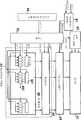
도 5는 독출 전용 제 1 메모리 뱅크 및 기입가능한 제2 메모리 뱅크로 이루어지는 보정 데이터 메모리부를 구비하는 화상 표시 장치의 전체 개념적 구조를 도시하는 블록도이다. 도 5의 화상 표시 장치는 m-라인 x n-컬럼 매트릭스로 배열된 발광 소자의 표시부(21), 각각의 발광 소자에 대응하는 보정 데이터를 저장하기 위한 보정 데이터 메모리부(26), 및 보정된 데이터에 기초하여 입력 화상 데이터를 보정하고 보정된 화상 데이터를 사용하여 표시부(21)상에 화상을 표시하기 위한 제어구동 회로를 구비한다. 제어구동 회로는 수직 드라이버부(22), 수평 드라이버부(23), 화상 데이터 보정부(24), 제어부(25), 화상 데이터 입력부(27), 통신제어부(28), 및 버퍼 메모리(20)를 구비한다. 화상 표시 장치에 있어서, 화상 데이터 입력부(27)로 입력되는 화상 데이터는 제어부(25)로 전송된다.Fig. 5 is a block diagram showing the overall conceptual structure of an image display device having a correction data memory section comprising a read-only first memory bank and a writable second memory bank. The image display device of FIG. 5 includes a
제어부(25)에 접속된 보정 데이터 메모리부(26)는 제 1 메모리 뱅크 및 제 2 메모리 뱅크를 가진다. 예를 들어, 보정 데이터 메모리부(26)는 EEPROM(데이터가 전기적으로 소거 또는 재기입될 수 있는 비휘발성 메모리)일 수 있다. 각 화소에 대한 휘도 변화를 보정하기 위한 데이터와 같은 제 1 보정 데이터는 제 1 메모리 뱅크내에 저장된다.The correction
본 실시예에 있어서, 휘도 변화 보정 데이터는 보정 데이터의 한 예로서 사용되지만, 본 발명은 이 형태의 보정 데이터에 제한되지 않는다.In the present embodiment, the luminance change correction data is used as an example of the correction data, but the present invention is not limited to this type of correction data.
화상 데이터 보정부(24)는 제어부(25) 및 버퍼 메모리(20)로의 각각의 화소 입력에 대한 제 1 보정 데이터 또는 제 2 보정 데이터에 따라 화상 데이터 입력부(27) 및 제어부(25)를 통해 각각의 화소 입력에 대해 화상 데이터를 보정한다. 화상 데이터 보정부(24)는 각 화소에 대응하는 화소 레벨데이터로서 보정된 데이터를 수평 드라이버부(23)로 출력한다. 이 화상 표시 장치 실시예에서 버퍼 메모리(20)는 1 내지 n 컬럼에 대응하는 1 내지 n 메모리 유니트(20)를 갖는다.The
수평 드라이버부(23)는 각각의 n-컬럼에 대응하는 n-메모리 유니트를 구비한다. 각 화소에 대응하는 입력 화소 레벨데이터는 이 화소를 포함하는 컬럼에 제공된 메모리에 저장된다. 수평 드라이버부(23)는 제어부(25)로부터의 제어 신호에 응답하여 메모리에 저장된 화소 레벨 데이터에 대응하는 화소 레벨 폭에 대한 지정된 전류 라인을 구동한다.The
또한, 수직 드라이버부(22)는 m-공통 소스 라인 각각에 접속된 m-스위칭 회로를 구비한다. 수직 드라이버부(22)는 전류 소스를 제어부(25)로부터의 제어 신호에 따라 특정된 공통 소스 라인에 접속한다.The vertical driver portion 22 also has an m-switching circuit connected to each of the m common source lines. The vertical driver portion 22 connects the current source to the common source line specified in accordance with the control signal from the
상술한 바와 같이, 제어부(25)는 보정 데이터메모리부(26)로부터 제 1 보정 데이터 또는 제 2 보정 데이터를 독출하여 이 데이터를 버퍼 메모리(20)에 저장한다. 제어부(20)는 또한, 버퍼 메모리(20) 및 화상 데이터보정부(24)에서 데이터 입력 출력 타이밍을 제어한다. 또한, 제어부(25)는 공통 소스 라인을 수직 드라이버부(22)내의 전류 소스와 접속하기 위해 스위칭을 제어한다. 최종적으로, 제어부(25)는 수평 제어부(23)내의 전류 라인을 구동하기 위해 스위칭을 제어한다. 이러한 방식으로, 제어부(25)는 표시부(21)의 각각의 화소를 순차적으로 조사하여 표시부(21)상의 입력 화상 데이터에 대응하는 화상을 표시한다.As described above, the
특히, 본 실시예의 화상 표시 장치는 아래의 특징을 갖는다.In particular, the image display device of this embodiment has the following features.
(1) 보정 데이터 메모리부(26)는 각각의 화소에 대응하는 미리 저장된 제 1 보정 데이터를 포함하는 제 1 메모리 뱅크 및 제 2 재기입가능한 메모리 뱅크를 구비한다.(1) The correction
(2) 화상 표시 장치는 통신제어부(28)를 구비한다. 통신 제어부(28)는 제 1 보정 데이터와 다른 제 2 보정 데이터가 제 2 메모리 뱅크에 기입될 수 있게 하고, 제 1 메모리 뱅크로의 기입을 금지한다.(2) The image display device includes a
(3) 제어부(25)는 제 1 메모리 뱅크에 저장된 제 1 보정 데이터 또는 제 2 메모리 뱅크에 저장된 제 2 보정 데이터중 어느 하나를 선택할 수 있다.(3) The
이러한 특징에 따르면, 도 5의 화상 표시 장치는 제 1 보정 데이터와 상이한 제 2 보정 데이터를 저장하기 위해 재기입가능한 제 2 메모리를 사용할 수 있고, 제 1 메모리 뱅크에 보유된 제 1 보정 데이터의 소거를 방지할 수 있다. 결과적으로, 제 1 보정 데이터 또는 제 2 보정 데이터중 어느 하나를 선택함으로써, 필요에 따라 화상 데이터를 보정할 수 있다.According to this feature, the image display device of FIG. 5 may use a rewritable second memory to store second correction data different from the first correction data, and erase the first correction data held in the first memory bank. Can be prevented. As a result, by selecting either the first correction data or the second correction data, the image data can be corrected as necessary.
실시예Example(2 개의 뱅크(2 banks보정correction 제어 회로에서의 휘도 Luminance in control circuit보정correction 데이터, 도 6) Data, FIG. 6)
이하, 도 6을 참조하여 본 발명의 화상 표시 장치의 한 실시예를 설명한다. 본 실시예의 화상 표시 장치는 표시부로서 LED 도트 매트릭스(41), 수직 드라이버부로서 공통 드라이버(42), 보정 데이터 메모리부로서 EEPROM(46), 화상 데이터 보정부로서 LED 드라이버 IC(44)의 보정 회로(49), 수평 드라이버부로서 LED 드라이버 IC(44)의 드라이버부(43), 제어부로서 명령 제어부(47) 및 제어부(45), 통신 제어부로서 직렬 통신 인터페이스(48), 및 버퍼 메모리로서 LED 드라이버 IC(44)의 시프트 레지스터(402) 및 레지스터(401)를 구비한다.Hereinafter, an embodiment of the image display device of the present invention will be described with reference to FIG. The image display device of this embodiment is a correction circuit of the
명령 제어부(47)는 공통 드라이버(42)에 공통 소스 라인 선택 신호(LINE ADR)를 입력하고, 조사 제어 신호를 각 드라이버부(43) 및 보정 회로(49)에 입력한다.The
이 실시예에 있어서, EEPROM(46)은 예를 들어, 보정 데이터의 선적시(shipping time) 공장(factory)에서 기입되는 BANK0, 및 사용자가 선적 후, 보정 데이터를 기입할 수 있는 BANK1을 포함한다. 제어부(45)는 직렬 통신 인터페이스(48)로부터의 제어 신호에 응답하여 BANK0 또는 BANK1 중 어느 하나로부터 보정 데이터를 선택한다. 이 실시예에 있어서, 기입 보호 설정은 재기입 데이터로부터 보정 데이터가 쉽핑 시간에 팩토리에서 기입된 BANK0으로 사용자가 접근하는 것을 금지시킨다.In this embodiment, the
이 실시예에서 직렬 통신 인터페이스(48)는 수신된 신호에 포함된 명령에 따라 여러 가지 처리를 수행한다. EEPROM(46)에 대한 독출 및 기입의 제어는 이하 상세히 설명된다.In this embodiment the
이하, EEPROM(46) 판독 및 기입을 제어하기 위해 EEPROM(46)의 구조 및 직렬 통신 인터페이스(48)를 상세히 설명한다. 도 7에 도시한 바와 같이, 직렬 통신 인터페이스(48)는 어드레스 레지스터(48b), 제어 레지스터(48e), 및 AND 논리 회로(48c 및 48d)를 포함하는 기입 보호 제어부(48f), 이외에 부수적으로 명령 제어(48a)로 구성된다.The structure of the
직렬 통신 인터페이스(48)로의 입력 신호(RXD)는 EEPROM (46)에 기입될 데이터를 명령하는 명령(기입 명령), 명령 제어부(48a)로 입력되는 기입가능한 통신 데이터를 포함한다. 도 7에 도시한 바와 같이, 기입가능한 데이터는 이곳에 데이터를 기입하기 위한 위치를 지정하는 개시 어드레스 데이터(도 7의 개시 어드레스) 및 기입될 데이터(도 7의 WRITE DATA)를 포함한다.The input signal RXD to the
기입 명령을 포함하는 RXD 입력 신호가 직렬 통신 인터페이스(48)에 의해 수신될 때, 명령 제어부(48a)는 기입 보호를 제거하기 위한 명령 데이터(WP 설정-제 거 명령 데이터)를 제어 레지스터(48e)로 출력한다. 명령 제어부(48a)는 또한 개시 어드레스 데이터의 최상위 비트(highest order bit)(A12)를 어드레스 레지스터(48b)로 출력하고, 논리 1을 AND 논리 회로(48c)로 출력한다. 또한, 명령 제어부(48a)는 기입가능한 통신 데이터를 EEPROM(46)의 어드레스 디코더(46a)로 출력한다.When an RXD input signal containing a write command is received by the
여기서, 최상위 비트(A12)가 0인 때, BANK0은 기입하기 위한 ROM 영역을 나타내고, 최상위 비트(A12)가 1인 때, BANK1은 기입하기 위한 ROM 영역을 나타낸다.Here, when the most significant bit A12 is 0, BANK0 indicates a ROM area for writing, and when the most significant bit A12 is 1, BANK1 indicates a ROM area for writing.
본 발명에 있어서, EEPROM(46)은 2 이상의 메모리 블록을 포함한다. 2 이상의 메모리 블록의 경우에 있어서, 최상위 2 이상 비트는 적용가능한 메모리 뱅크를 나타내기 위해 사용될 수 있다.In the present invention, the
제어 레지스터(48e)는 기입 보호 모드로 사전 설정되고, 기입 보호 모드를 나타내는 논리 0을 AND 논리 회로(48d)로 출력한다. 그러나, 기입 보호의 제거를 나타내는 명령 데이터(WP 설정 제거 명령 데이터)는 명령 제어부(48a)로부터 입력될 때, 기입 보호 제거를 나타내는 논리 1은 AND 논리 회로(48d)로 출력된다.The
논리 1이 BANK1을 나타내는 어드레스 레지스터를 통해 입력되고, 제어 레지스터(48e)가 기입 보호를 제거하기 위해 논리 1을 발생시킬 때, AND 논리 회로(48d)는 논리 1을 AND 논리 회로(48c)에 출력한다.When
명령 제어부(48a)가 논리 1을 발생시키고, 논리 1이 AND 논리 회로(48c)로 출력할 때, AND 논리 회로(48c)는 논리 1을 EEPROM(46)의 XWP 단자로 출력한다. 다른 모든 경우에 AND 논리 회로(48c)는 논리 0을 출력한다. 논리 1이 EEPROM(46)의 XWP 단자로 입력된 때, 기입 보호는 제거된다(WP-OFF). 논리 0이 EEPROM(46)의 XWP 단자로 입력된 때, 기입 보호는 유지된다(WP-ON).When the
XWP 단자는 EEPROM(46)의 기입 보호 단자이고, 데이터 기입이 이 단자에서 유효 또는 무효로 된다. XWP=0(LOW)인 때, EEPROM에 대한 데이터 기입은 무효로 되어 기입 보호모드가 설정된다. XWP=1(HIGH)인 때, EEPROM에 대한 데이터 기입은 유효로 되어 기입 보호모드가 설정되지 않는다.The XWP terminal is a write protection terminal of the
EEPROM(46)에서 BANK0과 BANK1사이의 스위칭은 기입가능한 통신 데이터내에 포함된 최상위 비트(A12)에 기초하여 어드레스 디코더(46a)에 의해 달성된다. 또한, 독출용 메모리 뱅크 선택은 최상위 비트(A12)를 사용하는 데이터 기입에서와 동일한 방식으로 수행된다. 즉, 메모리 뱅크 선택은 명령 제어부(48a)로부터 입력되는 기입가능한 통신 데이터에 포함된 최상위(A12)에 기초하여 EEPROM(46) 어드레스 디코더(46a)에 의해 수행될 수 있다.Switching between BANK0 and BANK1 in the
도 7에는 13 비트 와이드 어드레스 버스의 한 예가 도시되었지만, 최상위 비트에 의한 메모리 뱅크 선택은 13 비트 이상 또는 13 비트 이하의 방식에서와 동일하게 수행될 수 있다.Although an example of a 13-bit wide address bus is shown in FIG. 7, memory bank selection by most significant bit may be performed in the same manner as in a 13-bit or more or 13-bit or less manner.
상술한 EEPROM(46) 및 직렬 통신 인터페이스(48) 구성에 있어서, EEPROM(46) BANK0 보정 데이터는 항상 보호되어 있고, BANK1 보정데이터는 RXD 신호에 따라 재기입될 수 있다. 또한, BANK0 또는 BANK1 이들로부터 보정 데이터를 독출하도록 선택될 수 있다.In the above-described
직렬 통신 인터페이스(48)의 직접 접속에 의해 EEPROM(46)의 제어는 상술한 바와 같다. 그러나, EEPROM(46)은 도 6에 도시한 바와 같이, 중간 제어부(45)를 통해 EEPROM(46)과 직렬 통신 인터페이스(48)간의 접속에 의해 동일 형태로 제어될 수 있다. 특히, 직렬 통신 인터페이스(48)로부터 EEPROM(46)으로의 각각의 제어 신호는 직접 접속의 형태로 제어부(45)를 통해 EEPROM(46)으로 단순히 입력된다. EEPROM(46)으로부터 독출된 보정 데이터는 EEPROM(46)과 직렬 통신 인터페이스(48)사이에 접속된 제어부(45)에 의해 LED 드라이버 IC (44)의 시프트 레지스터(402)로 분기된다.The control of the
또한, 직렬 통신 인터페이스(48)에 의해 수신된 RXD 신호는 외부 콘트롤러(도시하지 않음)로부터 입력된다. 도 6에 도시한 바와 같이, EEPROM(46)으로부터 독출된 보정 데이터와 같은 데이터는 예를 들어, TXD 신호로서 직렬 통신 인터페이스(48)에 의해 외부 콘트롤러로 전송될 수 있다.In addition, the RXD signal received by the
상술한 도 6의 표시 장치 실시예에 있어서, 화상 데이터, 수직 동기 신호(Vsync), 및 수평 동기 신호(Hsync)는 화상 데이터 입력부(도시하지 않음)를 통해 제어부(47)로 입력된다. 입력 화상 데이터는 명령 제어부(47)로부터 LED 드라이버 IC(44) 보정 회로(49)로 전송된다.In the display device embodiment of FIG. 6 described above, the image data, the vertical synchronizing signal Vsync, and the horizontal synchronizing signal Hsync are input to the
또한, 수직 동기 신호(Vsync) 및 수평 동기 신호(Hsync)는 제어부(45), LED 드라이버 IC(44)의 보정 회로(49) 및 드라이버부(43), 및 공통 드라이버(42)로 입력된다.The vertical synchronizing signal Vsync and the horizontal synchronizing signal Hsync are input to the control unit 45, the
제어부(45)는 입력 수직 동기 신호(Vsync) 및 수평 동기 신호(Hsync)에 동기하여 표시 장치의 각각의 요소를 제어한다. 또한, 직렬 통신 인터페이스(48)에서 의 입력 신호에 따라 EEPROM(46) BANK0 또는 BANK1로부터 독출된 보정 데이터는 제어부(45) 명령에 따라 시프트 레지스터(402)로 순차적으로 전송된다. 보정 데이터의 한 개의 라인 값이 시프트 레지스터(402)로 전송된 후, 데이터는 대응 레지스터(401)를 통해 각 보정 회로(49)로 입력된다. 특히, 이 화상 데이터에 따른 화상 데이터 및 보정 데이터는 보정 회로(49)로 입력된다.The controller 45 controls each element of the display device in synchronization with the input vertical synchronization signal Vsync and the horizontal synchronization signal Hsync. Further, correction data read out from the
보정 회로(49)로의 화상 데이터 입력은 보정 데이터에 따라 보정 회로(49)에 의해 보정된다. 그 다음, 그 결과는 화소 레벨 데이터로서 취해지고, 각각의 드라이버부(43)로 입력한다. 보정된 화상 데이터(화소 레벨 데이터)에 기초하여 LED 도트 매트릭스(41)의 선정된 LED 라인은 화상 데이터에 따른 화상을 표시하기 위해 공통 드라이버(42) 및 각 드라이버부(43)에 의해 조사된다.The input of the image data to the
상술한 본 발명의 화상 표시 장치의 실시예에 있어서, EEPROM(46)의 BANK0에 저장된 보정 데이터, 예를 들어, 선적시 공장에서 기입된 보정 데이터는 소거되지 않고, 보유된다. 재기입가능한 BANK1은 예를 들어, 동작의 환경에 대해 설명하도록 수정된 보정 데이터를 저장하기 위해 사용자에 의해 사용될 수 있다. 필요에 따라 보정 데이터를 선택하는 것이 화상 데이터를 보정하기 위해 설정될 수 있다.In the embodiment of the image display device of the present invention described above, correction data stored in BANK0 of the
또한, 본 발명의 실시예의 구성에 있어서, EEPROM과 같은 단일 메모리 소자는 ROM 및 EEPROM과 같은 2 개의 메모리 소자를 제공하는 대신에 사용될 수 있다.In addition, in the configuration of the embodiment of the present invention, a single memory element such as EEPROM may be used instead of providing two memory elements such as ROM and EEPROM.
이 실시예에 있어서, 기입 보호 특징(WP 기능)을 갖는 EEPROM(46)이 기술되 었다. 기입 대 독출 전용 제어는 기입 인에이블 제어 신호의 출력 상태 즉, EEPROM 기입 동안 타이밍을 제어하는 XWE를 제어함으로써, WP 기능을 갖지 않고, EEPROM에서 달성될 수 있다. 예를 들어, 활성 LOW 기입 인에이블 펄스 XWE의 경우에, 직렬 통신 인터페이스가 기입 보호 모드내에서 기입 명령을 수신할 때, 동일 기입 보호 특징은 XWE를 항상 논리 HIGH로 설정함으로써, 달성될 수 있다.In this embodiment, an
특히, 본 발명은 상술한 실시예의 구조에 제한되지 않는다. 시스템이 최소한 1 개의 보정 데이터를 갖는 경우, 보정 데이터 메모리부는 기입 보호 영역 및 기입될 수 있는 영역을 구비한다.In particular, the present invention is not limited to the structure of the above-described embodiment. When the system has at least one correction data, the correction data memory section includes a write protection area and an area that can be written.
본 발명의 대규모 LED 표시상의 화상 표시는, 전체 화상을 LED 유니트 상의 부분 및 장착부로 분할하는 것이 바람직하다. 예를 들어, 사용자가 특정 구동조건으로 제 2 메모리 뱅크를 이미 설정한 대규모 LED 표시는 한 부분의 LED 유니트를 대체할 필요가 있다. 제 2 메모리 뱅크는 대체된 LED 유니트에 대해서만 조정하기 위해 재기입될 수 있고, 사용자의 구동조건에 대한 재조정은 용이하게 달성될 수 있다.In the image display on the large-scale LED display of the present invention, it is preferable to divide the entire image into portions and mounting portions on the LED unit. For example, a large LED display in which the user has already set the second memory bank to a particular driving condition needs to replace one part of the LED unit. The second memory bank can be rewritten to adjust only for the replaced LED unit, and the readjustment of the user's driving conditions can be easily achieved.
또한, 본 발명은 발광 다이오드를 사용하는 화상 표시 장치에 제한되지 않는다.In addition, the present invention is not limited to the image display apparatus using the light emitting diode.
도 8은 보정 데이터 메모리부로부터 1 개의 보정 데이터를 독출하여 각각의 시간동안, 1 개의 보정된 화상 데이터를 출력하는 화상 데이터 보정부를 갖는 화상 장치 실시예를 개략적으로 나타내는 블록도이다. 도 8에 도시한 화상 표시 장치는,FIG. 8 is a block diagram schematically showing an embodiment of an image device having an image data correction unit that reads one correction data from the correction data memory unit and outputs one corrected image data during each time period. In the image display device shown in Fig. 8,
(a) m-라인 x n-컬럼 매트릭스로 배열된 복수의 발광 소자로 이루어진 표시부(61),(a) a
(b) 표시부(61)의 각 라인 및 각 라인에 대한 소스 전류를 순차적으로 선택하는 수직 드라이버부(62),(b) a
(c) 선택된 라인에 대응하는 화상 데이터에 따른 표시부(61)가 컬럼에 구동 전류를 공급하는 수평 드라이버부(63),(c) the
(d) 각각의 화소에 대해 발광 소자의 특성의 변화에 따른 외부 입력 화상 데이터(IMDATA)를 보정하여 수평 드라이버부(63)에 보정된 데이터를 출력하는 화상 데이터 보정부(64), 및(d) an image data correction unit 64 for correcting the external input image data IMDATA according to the change of the characteristics of the light emitting element for each pixel and outputting the corrected data to the
(e) 화상 데이터 보정에 대한 보정 데이터를 보유하는 보정 데이터 메모리부 (66)를 구비한다. 이 시스템의 각 소자의 동작은 제어부(65)에 의해 제어된다.(e) A correction
화상 데이터 보정부(64)는 제어부(65)를 경유하여 보정 데이터 메모리부(66)로부터 보정 데이터(CRDATA)를 독출하고, 이 보정 데이터에 기초하여 제어부(65)를 경유하여 화상 데이터(IMDATA) 입력을 보정하고, 수평 드라이버부(63)로 보정된 화상 데이터를 출력한다. 총 mxn 화소의 보정 데이터는 모두 한번에 독출되는 것이 아니라, 다른 보정 데이터가 1 라인의 화상 데이터의 출력과 병렬로 한번에 1 라인 (n 화소)을 독출한다.The image data correction unit 64 reads the correction data CRDATA from the correction
정지 화상에 대한 화상 데이터의 경우에, 모두 임의의 버퍼 메모리를 제공하지 않고 화상 데이터를 보정할 수 있다. 그러나, 동화상의 경우에는 1 또는 2 라인의 보정 데이터를 저장할 수 있는 버퍼 메모리는 라인들 사이의 표시 시간 지연(time lag)을 방지하기에 바람직하다. 버퍼 메모리(60)는 예를 들어, 2 단의 상호접속된 레지스터(601 및 602)로서 구성될 수 있다.In the case of the image data for a still image, it is possible to correct the image data without providing any buffer memory. However, in the case of moving images, a buffer memory capable of storing one or two lines of correction data is preferable to prevent display time lag between lines. Buffer memory 60 may be configured, for example, as two stages of
독출 데이터 판독은 예를 들어, 이하의 방법으로 진행될 수 있다. 화상 데이터 보정부(64)는 3 단의 (상부 및 하부)의 상호 접속 레지스터(601 및 602)로 이루어진다. 제 1 레지스터(601)가 1 라인의 보정 데이터를 보정 회로(69)로 출력할 때, 보정 데이터의 다음 라인은 제 2 레지스터(602)로 독출된다. 제 1 레지스터(601)가 1 라인의 보정 데이터의 독출이 완료하고, 제 2 레지스터(602)가 1 라인의 보정 데이터의 독출을 완료한때 제 2 레지스터(602)의 내용이 제 1 레지스터(601)로 전송된다.Read data reading can be performed, for example, in the following manner. The image data correction unit 64 is composed of three stages of interconnect registers 601 and 602 (upper and lower). When the
데이터(n- 화소가 1 화소에 대한 비트 카운트를 측정하는)의 정확히 1 표시 라인 값에 대한 D-플립플롭 어레이는 예를 들어, 제 1 및 제 2 레지스터(601, 602)로서 사용될 수 있다. 보정 데이터 입력 와이어링을 간단히 하기 위해서는 시프트 레지스터를 형성하기 위해 마스터-슬레이브 순차에 따라 제 2의 레지스터(602)의 플립플롭을 접속하는 것이 바람직하다. 이러한 구성에 있어서, 제 2 레지스터(602)의 좌측 단부에서 플립플롭에 대한 보정 데이터 입력은 클럭(CLK) 타이밍에 동기하여 오른쪽으로 순차적으로 전송(시프트)하고, 데이터는 그러므로, 제 2 레지스터(602) 내로 독출된다. 그러므로, 보정 데이터 입력에 대한 각 컬럼으로 분기하는 버스 라인은 불필요하고, 클럭 신호를 각 플립플롭으로 공급하는 와이어링은 필요로 하는 모든 와이어링이다.The D-flip-flop array for exactly one display line value of the data (n-pixels measure the bit count for one pixel) can be used, for example, as the first and
도 9는 도 8에 도시한 화상 표시 장치의 상세한 구조를 도시하는 블록도이 다. 우선, 각 부의 구성이 설명된다. 표시부인 LED 도트 매트릭스(71)는 m-라인 x n-컬럼 매트릭스로 배열된 LED로 이루어진다. 각 라인에 배치된 모든 LED의 애노드는 1 개의 공통 소스 라인에 접속된다. 각 라인에 배치된 모든 LED의 캐소드는 1 개의 전류 라인에 접속된다. 수직 드라이버부인 공통 드라이버(72)는 M-스위칭 회로를 구비한 전류 스위칭 및 관련 전류 소스를 포함한다. 공통 드라이버(72)는 공통 소스 라인을 전류 소스에 접속함으로써, 공통 소스 라인에 접속된 LED에 전류를 공급한다. 수평 드라이버부인 드라이버 회로(73)는 보정 회로(79)로부터의 화상 데이터 출력의 화소 레벨 폭에 따른 각각 컬럼에 대한 구동 전류의 온 및 오프를 제어하는 정 전류 제어 회로를 포함한다.FIG. 9 is a block diagram showing the detailed structure of the image display device shown in FIG. First, the structure of each part is demonstrated. The
화상 데이터 보정부는 한번에 1 라인의 입력 화상 데이터를 보정하여 순차적으로 출력하는 보정 회로(79), 및 보정 데이터를 저장하기 위해 버퍼 메모리인 레지스터(701) 및 시프트 레지스터(702)로 이루어진다. 각 레지스터(701) 및 시프트 레지스터(702)는 1 컬럼의 화소에 대한 비트 수에 대응하는 플립플롭을 갖는다. 또한, 각 레지스터(701)의 플립플롭은 시프트 레지스터 (702)의 대응 플립플롭에 접속된다. 제어부는 제어회로(77)(CTL) 및 직접 메모리 억세스 콘트롤러(DMAC) (75)로 이루어진다. 보정 데이터 메모리부인 ROM(76)은 EEPROM과 같은 메모리를 포함한다. LED 도트 매트릭스(71)의 각 LED의 발광 특성의 변화로 인한 휘도 차이를 보정하기 위한 휘도 보정 데이터는 ROM(76)에 저장된다. 보정 데이터는 각각의 화소 및 각각의 컬러에 따른 각각의 LED에 대한 구동 전류를 제어하기 위한 데이터이다. LED 조사 시간 또는 구동 전류 단독 대신에 조사 시간과 구동 전류의 조합 을 제어하기 위한 데이터이 적절한 데이터이다.The image data correction unit includes a
드라이버 회로(73), 보정 회로(79), 레지스터(701), 및 시프트 레지스터 (702)는 LED 도트 매트릭스(71)의 각 컬럼에 제공되어, 각 컬럼에 제공되고, 각 컬럼에서 LED 드라이버 IC(k)(k=1 내지 n)내에 포함된다. 각각의 컬럼에서의 시프트 레지스터(702)는 데이터 시프팅을 허용하도록 함께 접속된다. 또한, 적절한 수의 컬럼에서 LED 드라이버 IC의 수, 드라이버 회로 등을 줄이기 위해 1 개의 LED 드라이버 IC내로 조합될 수 있다.The
보정 데이터 ROM(76)에의 기입 및 이곳으로부터의 독출은 직렬 통신 인터페이스인 SCI(78)을 통해 화상 데이터와 독립적으로 수행될 수 있다. ROM(76)에의 기입은 또한, 직접 전송 방법을 사용하여 ROM(76)에 직접 접속하거나, 여러 형태의 인터페이스 및 병렬 버스를 경유하여 수행될 수 있다. 데이터가 ROM(76)에 기입되고, 보정 데이터가 ROM(76)으로부터 독출될 때, DMAC(75)에 의한 데이터 전송은 차단되고, SCI(78)을 통한 데이터 수신은 우선권이 주어진다. 이것은 ROM(76) 억세스에 대한 경쟁을 제어한다.Writing to and reading from the
이 실시예의 화상 데이터의 화상 데이터의 흐름은 아래와 같이 진행한다. 화상 데이터(IMDATA)는 CTL(77)로 입력되어 보정 회로(79)로 분배된다. 화상 데이터의 각 라인은 보정 회로(79)에 의해 보정된 후, 이는 드라이버 회로(73)로 출력된다.The flow of image data of the image data of this embodiment proceeds as follows. The image data IMDATA is input to the
그 다음, 보정 데이터의 흐름은 도 10의 타이밍도를 참조하여 설명된다. 설명을 간단히 하기 위해, 도 10은 3 개의 공통 소스 라인(#1 내지 #2)의 조사의 경 우를 순서에 따라 도시한다. 수평 및 수직 화상 타이밍 데이터(Vsync 및 Hsync)가 CTL(77)로 입력될 때 라인(#0) 보정 데이터는 시프트 레지스터(702)내로 독출되도록 개시한다. CTL(77)로의 Vsync 입력은 LINE ADR 신호로서 공통 드라이버(72)로 전송되고, Hsync는 BLANK 신호로서 드라이버 회로(73) 및 보정 회로(79)로 전송된다.Next, the flow of the correction data is described with reference to the timing diagram of FIG. For simplicity of explanation, FIG. 10 shows, in order, the case of irradiation of three common
(1) 우선, CTL(77)은 ROM(76)으로부터 라인(#0) 보정 데이터를 독출하기 위한 개시 어드레스(ADDRESS)를 DMAC(75)내로 입력한다. DMAC(75)는 데이터 입력-출력 버스(DIO)를 경유하여 ROM(76)에 독출하기 위한 개시 어드레스를 기입하고, 기입 인에이블 신호(XWE)를 ROM(76)에 발생한다. 도 11에 개략적으로 도시한 바와 같이, ROM(76)에 대한 개시 어드레스는 선택된 라인에 대응하는 ROM 메모리 맵내의 보정 데이터의 개시 어드레스를 나타낸다. CTL(77)은 Vsync 및 Hsync로부터 결정된 라인 수에 대응하는 보정 데이터를 독출하기 위한 개시 어드레스를 발생한다.(1) First, the
(2) 독출하기 위한 개시 어드레스를 기입한 후, DMAC(75)는 데이터 버스(DIO)를 경유하여 ROM(76)으로부터 라인(#0) 보정 데이터를 독출하고, 독출 인에이블 신호(XOE)를 발생한다. ROM(76)은 XOE 상의 LOW 펄스 카운트에 대응하는 보정 데이터를 순차적으로 출력한다.(2) After writing the start address for reading out, the
(3) DMAC(75)내로의 라인(#0) 보정 데이터(CRDATA) 판독은 드라이버 IC[74(k)]내의 시프트 레지스터(702)전송된다. 보정 데이터는 클럭(CLK)과 동기하는 시간에 1 비트를 시프트함으로써, 시프트 레지스터(702)내로 순차적으로 전송된다.(3) The read of the
라인(#0)보정 데이터가 시프트 레지스터(702)내로 독출될지라도, 레지스터(701)는 최종 라인인 라인(#2) 보정 데이터를 보유한다. 레지스터(701)에 유지된 라인(#2) 보정 데이터는 드라이버 회로(73)에 출력하고, 라인(#2) LED가 조사되고, 보정 데이터는 레지스터(701)내에 유지된다. 그 다음 Hsync 펄스가 입력될 때, 래치 신호(LATCH)는 DMAC(75)로부터 레지스터(701)로 발생되고, 시프트 레지스터(702)에 저장된 라인(#0) 보정 데이터는 한번에 레지스터(701)로 전송되어 라인 (#0) LED 조사가 개시된다. 그 다음, 라인(#1) 보정 데이터를 독출하기 위한 개시 어드레스는 CTL(75)로부터 DMAC(75)로 입력된다. 상술한 방식으로, DMAC(75)는 ROM(76)으로부터 라인 (#1) 보정 데이터를 독출하여 이를 시프트 레지스터(702)내에 기입한다.Although the
이러한 방식으로, 이전의 라인이 조사될지라도, 조사될 다음 라인의 각 화소를 보정하기 위한 데이터의 입력이 완료된다. 시프트 레지스터(702)로의 보정 데이터 입력은 1 라인으로부터 그 다음 라인으로의 스위칭 조사 바로 전에 레지스터(701)내로 전송되어 유지된다. 이 보유된 보정 데이터에 기초하여 보정 회로(79)는 활성 표시 라인의 각 LED의 휘도 변화에 대해 보상함으로써, 화상 데이터를 보정한다. 이들 동작의 연속적인 반복에 의해 LED 휘도 보정은 전체 표시 장치에 걸쳐 달성된다.In this way, even if the previous line is irradiated, the input of data for correcting each pixel of the next line to be irradiated is completed. Correction data input to the
우발적으로 시프트 레지스터(702)내로의 보정 데이터의 전송은 1 표시 라인의 조사하는 시간내에 완료되어야 한다. 그러므로, 라인당 너무 많은 화상 데이터를 갖지 않는 LED 유니트를 사용하는 대형 스크린 LED 표시 장치와 같은 화상 데이 터는 시프트 레지스터를 경유하여 데이터 전송을 구현하는데 적합하다.Incidentally, the transfer of correction data into the
여기서, 데이터가 직렬 형태로 독출되는 직렬 EEPROM은 ROM(76)으로서 기술된다. 그러나, n-비트 어드레스 및 데이터 버스를 갖는 EEPROM이 ROM(76)으로서 사용될 수 있지만, 데이터 전송은 병렬 버스를 통해 수행될 수도 있다.Here, the serial EEPROM from which data is read in serial form is described as the
전 색(full color) 표시 장치의 경우에 있어서, 각각의 화소는 3 RGB 컬러 LED로 이루어진다. 각각의 RGB 컬러에 대한 화상 데이터는 상술한 방식으로 보정될 수 있다.In the case of a full color display, each pixel consists of 3 RGB color LEDs. Image data for each RGB color can be corrected in the manner described above.
상술한 실시예들은 각각의 특성을 쉽게 이해되도록 별도의 실시예로서 제공되었다. 도 1 및 도 2에 도시된 화상 표시 장치는 축적된 전하를 방전하기 위해 발광 소자의 공통 소스 라인을 접지에 접속하는 스위칭부를 갖는다. 도 5 및 도 6에 도시한 화상 표시 장치는 보정 데이터를 저장하여 메모리에의 기입을 금지하는 제 1 메모리 뱅크 및 기입될 수 있는 제 2 메모리 뱅크를 갖는 보정 데이터 메모리부로 구성된다. 도 8 및 도 9에 도시한 화상 표시 장치에 있어서는 각각의 시간에 1 라인의 보정된 화상 데이터는 화상 데이터 보정부에서 수평 드라이버부로 출력되고, 보정 데이터의 그 다음 라인은 보정 데이터 메모리부로부터 독출된다. 그러나, 가장 이상적인 화상 표시 장치는 상술한 모든 회로를 구비한 장치에 의해 실현될 수 있다.The above-described embodiments are provided as separate embodiments so that each characteristic is easily understood. The image display device shown in Figs. 1 and 2 has a switching section which connects a common source line of the light emitting element to ground to discharge the accumulated charge. The image display device shown in Figs. 5 and 6 is composed of a correction data memory section having a first memory bank for storing correction data and prohibiting writing to the memory and a second memory bank that can be written. In the image display apparatus shown in Figs. 8 and 9, one line of corrected image data at each time is output from the image data correcting section to the horizontal driver section, and the next line of correction data is read out from the correcting data memory section. . However, the most ideal image display device can be realized by a device having all the circuits described above.
본 발명에 따른 화상 표시 장치에 따르면, 비활성 상태시, 발광 소자 및 그 주변에 축적된 전하는 비활성 상태중에 스위칭 회로를 경유하여 방전된다. 결과적 으로, 규정된 발광 소자의 활성 조사중에 축적된 전하의 효과는 필연적으로 제거되고, 고화질의 화상 표시 장치가 실현된다.According to the image display device according to the present invention, in the inactive state, the charges accumulated in the light emitting element and its surroundings are discharged through the switching circuit during the inactive state. As a result, the effect of the charge accumulated during the active irradiation of the defined light emitting element is necessarily eliminated, and a high quality image display device is realized.
본 발명의 화상 표시 장치의 구동방법에 따르면, 활성 상태시, 발광 소자 및 그 주변에 축적된 전하는 비활성 상태중에 스위칭 회로부를 통해 방전될 수 있다. 결과적으로, 규정된 발광 소자의 활성 조사중에 축적된 전하의 효과는 필연적으로 제거될 수 있어, 고화질의 화상 표시 장치의 구동방법이 제공된다.According to the driving method of the image display device of the present invention, in the active state, the light emitting element and the electric charge accumulated in the vicinity thereof can be discharged through the switching circuit portion during the inactive state. As a result, the effect of the charge accumulated during the active irradiation of the prescribed light emitting element can be inevitably eliminated, thereby providing a driving method of a high quality image display device.
본 발명은 본 발명의 필수적인 특성의 범주를 벗어나지 않고서도 변형될 수 있기 때문에, 본 실시예는 상술한 상세한 설명에 의해 한정되는 것이 아니라 첨부된 청구의 범위에 의해 정해지고, 청구의 범위내에 속하는 모든 변형 또는 이들과의 등가물은 본 청구의 범위에 의해 포함된다.Since the present invention can be modified without departing from the scope of the essential features of the invention, the present embodiment is not to be limited by the foregoing detailed description, but is defined by the appended claims, and all of the claims fall within the scope of the claims. Modifications or equivalents thereof are encompassed by the claims.
Claims (39)
Translated fromKoreanApplications Claiming Priority (6)
| Application Number | Priority Date | Filing Date | Title |
|---|---|---|---|
| JP194551 | 1999-07-08 | ||
| JP19455199 | 1999-07-08 | ||
| JP30313499AJP3358600B2 (en) | 1999-10-25 | 1999-10-25 | Image display device with image data correction function |
| JP302493 | 1999-10-25 | ||
| JP303134 | 1999-10-25 | ||
| JP30249399AJP3679657B2 (en) | 1999-10-25 | 1999-10-25 | Image display device |
Publications (2)
| Publication Number | Publication Date |
|---|---|
| KR20010029903A KR20010029903A (en) | 2001-04-16 |
| KR100618252B1true KR100618252B1 (en) | 2006-09-04 |
Family
ID=27326960
Family Applications (1)
| Application Number | Title | Priority Date | Filing Date |
|---|---|---|---|
| KR1020000038850AExpired - LifetimeKR100618252B1 (en) | 1999-07-08 | 2000-07-07 | Image display apparatus and its method of operation |
Country Status (8)
| Country | Link |
|---|---|
| US (2) | US6545652B1 (en) |
| EP (3) | EP1612764B1 (en) |
| KR (1) | KR100618252B1 (en) |
| CN (3) | CN100336093C (en) |
| CA (1) | CA2313550C (en) |
| MY (1) | MY124036A (en) |
| SG (2) | SG98413A1 (en) |
| TW (1) | TW468143B (en) |
Families Citing this family (70)
| Publication number | Priority date | Publication date | Assignee | Title |
|---|---|---|---|---|
| JP3737889B2 (en)* | 1998-08-21 | 2006-01-25 | パイオニア株式会社 | Light emitting display device and driving method |
| US6724149B2 (en)* | 1999-02-24 | 2004-04-20 | Sanyo Electric Co., Ltd. | Emissive display device and electroluminescence display device with uniform luminance |
| US7088322B2 (en) | 2000-05-12 | 2006-08-08 | Semiconductor Energy Laboratory Co., Ltd. | Semiconductor device |
| JP3906653B2 (en)* | 2000-07-18 | 2007-04-18 | ソニー株式会社 | Image display device and manufacturing method thereof |
| US7292209B2 (en)* | 2000-08-07 | 2007-11-06 | Rastar Corporation | System and method of driving an array of optical elements |
| GB0105148D0 (en)* | 2001-03-02 | 2001-04-18 | Koninkl Philips Electronics Nv | Active Matrix Display Device |
| US6943761B2 (en)* | 2001-05-09 | 2005-09-13 | Clare Micronix Integrated Systems, Inc. | System for providing pulse amplitude modulation for OLED display drivers |
| TWI221268B (en) | 2001-09-07 | 2004-09-21 | Semiconductor Energy Lab | Light emitting device and method of driving the same |
| US6777885B2 (en)* | 2001-10-12 | 2004-08-17 | Semiconductor Energy Laboratory Co., Ltd. | Drive circuit, display device using the drive circuit and electronic apparatus using the display device |
| WO2003034384A2 (en) | 2001-10-19 | 2003-04-24 | Clare Micronix Integrated Systems, Inc. | Method and system for precharging oled/pled displays with a precharge latency |
| US20030169219A1 (en)* | 2001-10-19 | 2003-09-11 | Lechevalier Robert | System and method for exposure timing compensation for row resistance |
| US7742064B2 (en)* | 2001-10-30 | 2010-06-22 | Semiconductor Energy Laboratory Co., Ltd | Signal line driver circuit, light emitting device and driving method thereof |
| US7576734B2 (en)* | 2001-10-30 | 2009-08-18 | Semiconductor Energy Laboratory Co., Ltd. | Signal line driving circuit, light emitting device, and method for driving the same |
| JP3923341B2 (en) | 2002-03-06 | 2007-05-30 | 株式会社半導体エネルギー研究所 | Semiconductor integrated circuit and driving method thereof |
| JP3498745B1 (en)* | 2002-05-17 | 2004-02-16 | 日亜化学工業株式会社 | Light emitting device and driving method thereof |
| KR101102372B1 (en)* | 2003-01-17 | 2012-01-05 | 가부시키가이샤 한도오따이 에네루기 켄큐쇼 | Semiconductor device and light-emitting device |
| JP4530622B2 (en)* | 2003-04-10 | 2010-08-25 | Okiセミコンダクタ株式会社 | Display panel drive device |
| KR100903099B1 (en)* | 2003-04-15 | 2009-06-16 | 삼성모바일디스플레이주식회사 | Method and device for driving an electroluminescent display panel that efficiently performs booting |
| JP2005004117A (en)* | 2003-06-16 | 2005-01-06 | Hitachi Ltd | Display device |
| JP2005004118A (en)* | 2003-06-16 | 2005-01-06 | Hitachi Ltd | Display device |
| CN100371975C (en)* | 2003-06-25 | 2008-02-27 | 盛群半导体股份有限公司 | driving method of light emitting diode |
| US7961160B2 (en)* | 2003-07-31 | 2011-06-14 | Semiconductor Energy Laboratory Co., Ltd. | Display device, a driving method of a display device, and a semiconductor integrated circuit incorporated in a display device |
| RU2006126711A (en)* | 2003-12-15 | 2008-01-27 | Марк ИШАКОВ (IL) | UNIVERSAL MULTIFUNCTION KEY OF INPUT / OUTPUT DEVICES |
| US20050272474A1 (en)* | 2004-06-03 | 2005-12-08 | Nokia Corporation | Controlling the appearance of a hand-portable electronic device |
| JP2005351920A (en)* | 2004-06-08 | 2005-12-22 | Semiconductor Energy Lab Co Ltd | Control circuit for display device and display device and electronic equipment containing the same and driving method for the same |
| CN1860512A (en)* | 2004-06-18 | 2006-11-08 | 株式会社东芝 | Video display device and luminance characteristic correcting method of video display device |
| US7372430B2 (en)* | 2004-07-15 | 2008-05-13 | Nittoh Kogaku K.K. | Light emitting device and light receiving and emitting driving circuit |
| US7317433B2 (en)* | 2004-07-16 | 2008-01-08 | E.I. Du Pont De Nemours And Company | Circuit for driving an electronic component and method of operating an electronic device having the circuit |
| JP2006047510A (en)* | 2004-08-02 | 2006-02-16 | Oki Electric Ind Co Ltd | Display panel driving circuit and driving method |
| US20060092329A1 (en)* | 2004-10-29 | 2006-05-04 | Canon Kabushiki Kaisha | Image display apparatus and correction apparatus thereof |
| US7647083B2 (en) | 2005-03-01 | 2010-01-12 | Masimo Laboratories, Inc. | Multiple wavelength sensor equalization |
| KR101136286B1 (en)* | 2005-10-17 | 2012-04-19 | 엘지디스플레이 주식회사 | Flat Display Apparatus And Picture Quality Controling Method Thereof |
| KR101182307B1 (en)* | 2005-12-07 | 2012-09-20 | 엘지디스플레이 주식회사 | Flat Display Panel, Picture Quality Controlling Apparatus thereof and Picture Quality Controlling Method thereof |
| KR100815587B1 (en)* | 2006-01-17 | 2008-03-20 | 빛샘전자주식회사 | Fault detection device and method for light emitting diode dot matrix module |
| US8265723B1 (en) | 2006-10-12 | 2012-09-11 | Cercacor Laboratories, Inc. | Oximeter probe off indicator defining probe off space |
| CN101004894B (en)* | 2006-10-20 | 2010-05-19 | 北京巨数数字技术开发有限公司 | Scanning type LED display device and method for eliminating forward hidden brightness of scanning type LED display device |
| CN101866613B (en)* | 2007-01-08 | 2012-05-23 | 北京巨数数字技术开发有限公司 | Scanning type LED display device and method for eliminating forward moving hidden brightness thereof |
| US10499029B2 (en)* | 2007-01-09 | 2019-12-03 | Capso Vision Inc | Methods to compensate manufacturing variations and design imperfections in a display device |
| EP2139383B1 (en) | 2007-03-27 | 2013-02-13 | Masimo Laboratories, Inc. | Multiple wavelength optical sensor |
| US8374665B2 (en) | 2007-04-21 | 2013-02-12 | Cercacor Laboratories, Inc. | Tissue profile wellness monitor |
| US7569997B2 (en)* | 2007-05-06 | 2009-08-04 | Ascend Visual System, Inc. | Self-calibrated integration method of light intensity control in LED backlighting |
| US8049709B2 (en) | 2007-05-08 | 2011-11-01 | Cree, Inc. | Systems and methods for controlling a solid state lighting panel |
| CN101408684B (en)* | 2007-10-12 | 2010-08-25 | 群康科技(深圳)有限公司 | Liquid crystal display apparatus and drive method thereof |
| CN101217022B (en)* | 2008-01-04 | 2010-06-02 | 深圳市奥拓电子有限公司 | A LED display screen display calibration system and calibration method |
| JP4884413B2 (en)* | 2008-03-13 | 2012-02-29 | 日本テキサス・インスツルメンツ株式会社 | LED control device |
| TWI394125B (en)* | 2008-04-11 | 2013-04-21 | Chunghwa Picture Tubes Ltd | Back light module |
| TW200947350A (en)* | 2008-05-09 | 2009-11-16 | Nexcom Int Co Ltd | Video signal processing system and method |
| US8599625B2 (en)* | 2008-10-23 | 2013-12-03 | Marvell World Trade Ltd. | Switch pin multiplexing |
| KR100893892B1 (en)* | 2008-11-17 | 2009-04-20 | 진영정보통신 주식회사 | LED display board with remote control |
| JP2010140953A (en)* | 2008-12-09 | 2010-06-24 | Sanyo Electric Co Ltd | Light-emitting element driving circuit |
| CN101447173B (en)* | 2008-12-22 | 2013-11-06 | 范红霞 | System for adjusting point-to-point brightness in a plant and method |
| US9839381B1 (en) | 2009-11-24 | 2017-12-12 | Cercacor Laboratories, Inc. | Physiological measurement system with automatic wavelength adjustment |
| WO2011069122A1 (en) | 2009-12-04 | 2011-06-09 | Masimo Corporation | Calibration for multi-stage physiological monitors |
| DE102010055797A1 (en)* | 2010-12-23 | 2012-06-28 | Continental Automotive Gmbh | Electric motor vehicle with a display device |
| CN103400549B (en)* | 2012-09-29 | 2016-04-13 | 西安诺瓦电子科技有限公司 | The LED pixel correction coefficient method for uploading of LED display |
| TWI545552B (en)* | 2014-03-27 | 2016-08-11 | Sitronix Technology Corp | Drive color display display black and white gray image of the drive circuit and its data conversion circuit |
| KR20170093832A (en)* | 2014-11-28 | 2017-08-16 | 가부시키가이샤 한도오따이 에네루기 켄큐쇼 | Image processing device, display system, and electronic device |
| CN108735137B (en)* | 2017-06-07 | 2022-03-22 | 浙江苏泊尔家电制造有限公司 | Circuit system for household appliance display screen and cooking appliance |
| TWI633531B (en)* | 2017-10-13 | 2018-08-21 | 點晶科技股份有限公司 | Light emitting diode driving circuit and light emitting diode display device |
| KR102519929B1 (en)* | 2017-12-18 | 2023-04-10 | 삼성전자주식회사 | Display apparatus |
| CN108230992B (en)* | 2017-12-26 | 2020-03-06 | 青岛海尔科技有限公司 | Light-emitting tube matrix driving method, device and storage medium |
| JP2019149767A (en)* | 2018-02-28 | 2019-09-05 | パナソニック液晶ディスプレイ株式会社 | Display device calibration system, display device, photographing device, server device, and display device calibration method |
| US10699631B2 (en)* | 2018-09-12 | 2020-06-30 | Prilit Optronics, Inc. | LED sensing system and display panel sensing system |
| KR102657536B1 (en)* | 2018-10-24 | 2024-04-12 | 엘지디스플레이 주식회사 | Display panel and method of deactivating light emitting diode in display panel |
| CN111462682B (en)* | 2020-05-06 | 2024-12-27 | 利亚德光电股份有限公司 | Light emitting diode LED drive circuit, light emitting diode LED display system |
| CN112599106B (en)* | 2020-12-31 | 2022-07-08 | 绵阳惠科光电科技有限公司 | Display panel, driving method thereof and display device |
| US11837181B2 (en)* | 2021-02-26 | 2023-12-05 | Nichia Corporation | Color balancing in display of multiple images |
| EP4322151A4 (en)* | 2021-04-08 | 2025-01-29 | LG Electronics Inc. | DISPLAY DEVICE AND IMAGE DISPLAY DEVICE COMPRISING SAME |
| CN115394244B (en)* | 2022-10-28 | 2023-01-24 | 惠科股份有限公司 | Display driving circuit, display driving method and display device |
| CN117079577B (en)* | 2023-10-18 | 2024-03-19 | 惠科股份有限公司 | Display panel, display panel driving method and display device |
Citations (8)
| Publication number | Priority date | Publication date | Assignee | Title |
|---|---|---|---|---|
| US4864182A (en)* | 1987-01-06 | 1989-09-05 | Sharp Kabushiki Kaisha | Driving circuit for thin film EL display device |
| KR940004520A (en)* | 1992-08-20 | 1994-03-15 | 쓰지 하루오 | Display |
| EP0702347A1 (en)* | 1994-07-18 | 1996-03-20 | Kabushiki Kaisha Toshiba | Dot-matrix LED display and method of adjusting brightness of the same |
| US5581160A (en)* | 1994-02-09 | 1996-12-03 | Nec Corporation | Method and apparatus for lighting an EL element |
| EP0784305A1 (en)* | 1996-01-11 | 1997-07-16 | Motorola, Inc. | Organic light emitting diode array drive apparatus |
| JPH09305146A (en)* | 1996-05-15 | 1997-11-28 | Pioneer Electron Corp | Display device |
| US5844368A (en)* | 1996-02-26 | 1998-12-01 | Pioneer Electronic Corporation | Driving system for driving luminous elements |
| KR19990030246A (en)* | 1997-09-30 | 1999-04-26 | 가시오 가즈오 | Driving circuit and driving method of display element |
Family Cites Families (32)
| Publication number | Priority date | Publication date | Assignee | Title |
|---|---|---|---|---|
| US3696393A (en)* | 1971-05-10 | 1972-10-03 | Hughes Aircraft Co | Analog display using light emitting diodes |
| DE3222973A1 (en) | 1982-05-26 | 1983-12-01 | BBC Aktiengesellschaft Brown, Boveri & Cie., 5401 Baden, Aargau | Circuit arrangement for displaying binary signals by means of antiparallel-connected pairs of light-emitting diodes |
| DE3400056A1 (en)* | 1984-01-03 | 1985-07-11 | Robert Bosch Gmbh, 7000 Stuttgart | Multi-digit digital indicator |
| FR2579807B1 (en) | 1985-03-26 | 1987-12-18 | Radiotechnique Compelec | COLORFUL LIGHT SIGN FOR INFORMATION DISPLAY |
| US4825201A (en)* | 1985-10-01 | 1989-04-25 | Mitsubishi Denki Kabushiki Kaisha | Display device with panels compared to form correction signals |
| DE4021333C1 (en)* | 1990-07-04 | 1991-11-07 | Telenorma Gmbh, 6000 Frankfurt, De | |
| JPH0498089A (en) | 1990-08-17 | 1992-03-30 | Toshiba Corp | Condenser |
| JPH04257464A (en)* | 1991-02-08 | 1992-09-11 | Ricoh Co Ltd | LED array drive device |
| JPH05265419A (en) | 1992-03-19 | 1993-10-15 | Hitachi Ltd | Display controller |
| JP3268001B2 (en)* | 1992-03-25 | 2002-03-25 | シャープ株式会社 | LED dot matrix type display device |
| JPH0667622A (en)* | 1992-08-21 | 1994-03-11 | Sharp Corp | Led display panel driver circuit |
| JPH06186942A (en)* | 1992-12-15 | 1994-07-08 | Ricoh Co Ltd | Display device |
| DE69420437T2 (en)* | 1993-02-19 | 1999-12-23 | Asahi Glass Co. Ltd., Tokio/Tokyo | Display device and method for generating data signals for a display device |
| JP3180858B2 (en) | 1993-05-28 | 2001-06-25 | 横河電機株式会社 | Liquid crystal display |
| JPH07199861A (en)* | 1993-12-30 | 1995-08-04 | Takiron Co Ltd | Emission luminous intensity adjusting device for dot matrix light emitting diode display unit |
| US5727192A (en)* | 1995-03-24 | 1998-03-10 | 3Dlabs Inc. Ltd. | Serial rendering system with auto-synchronization on frame blanking |
| JPH0934406A (en)* | 1995-07-14 | 1997-02-07 | Matsushita Electric Ind Co Ltd | Full color LED panel |
| DE69531294D1 (en)* | 1995-07-20 | 2003-08-21 | St Microelectronics Srl | Method and apparatus for unifying brightness and reducing phosphorus degradation in a flat image emission display device |
| US5748160A (en) | 1995-08-21 | 1998-05-05 | Mororola, Inc. | Active driven LED matrices |
| JPH09244596A (en) | 1996-03-12 | 1997-09-19 | Fuji Xerox Co Ltd | Display control device |
| JPH09258693A (en) | 1996-03-26 | 1997-10-03 | Stanley Electric Co Ltd | Full color LED dot matrix display |
| JP4059537B2 (en) | 1996-10-04 | 2008-03-12 | 三菱電機株式会社 | Organic thin film EL display device and driving method thereof |
| JPH10341358A (en) | 1997-06-06 | 1998-12-22 | Nec Corp | Image quality control system |
| JPH11161219A (en) | 1997-09-10 | 1999-06-18 | Toray Ind Inc | Light emitting device drive circuit |
| JP2993475B2 (en) | 1997-09-16 | 1999-12-20 | 日本電気株式会社 | Driving method of organic thin film EL display device |
| JP3765918B2 (en)* | 1997-11-10 | 2006-04-12 | パイオニア株式会社 | Light emitting display and driving method thereof |
| US6317138B1 (en)* | 1998-03-31 | 2001-11-13 | Sony Corporation | Video display device |
| JP3568097B2 (en)* | 1998-04-22 | 2004-09-22 | パイオニア株式会社 | Light emitting display and driving method thereof |
| KR100598137B1 (en)* | 1998-09-16 | 2006-07-07 | 소니 가부시끼 가이샤 | Display apparatus |
| JP2000098974A (en)* | 1998-09-24 | 2000-04-07 | Pioneer Electronic Corp | Capacitive light emitting element display device and its drive method |
| JP2000221935A (en) | 1999-02-04 | 2000-08-11 | Victor Co Of Japan Ltd | Matrix type display device |
| JP3341735B2 (en)* | 1999-10-05 | 2002-11-05 | 日本電気株式会社 | Driving device for organic thin film EL display device and driving method thereof |
- 2000
- 2000-07-03MYMYPI20003033patent/MY124036A/enunknown
- 2000-07-03SGSG200003688Apatent/SG98413A1/enunknown
- 2000-07-03SGSG200300700Apatent/SG119173A1/enunknown
- 2000-07-04TWTW089113250Apatent/TW468143B/ennot_activeIP Right Cessation
- 2000-07-05EPEP05012344.7Apatent/EP1612764B1/ennot_activeExpired - Lifetime
- 2000-07-05EPEP05012345.4Apatent/EP1594117B1/ennot_activeExpired - Lifetime
- 2000-07-05EPEP00114437Apatent/EP1067505A3/ennot_activeWithdrawn
- 2000-07-06CACA002313550Apatent/CA2313550C/ennot_activeExpired - Lifetime
- 2000-07-06USUS09/610,991patent/US6545652B1/ennot_activeExpired - Lifetime
- 2000-07-07KRKR1020000038850Apatent/KR100618252B1/ennot_activeExpired - Lifetime
- 2000-07-07CNCNB03127871XApatent/CN100336093C/ennot_activeExpired - Fee Related
- 2000-07-07CNCNB001204289Apatent/CN1195292C/ennot_activeExpired - Lifetime
- 2000-07-07CNCNB031278728Apatent/CN100336094C/ennot_activeExpired - Lifetime
- 2002
- 2002-12-12USUS10/317,041patent/US6847342B2/ennot_activeExpired - Lifetime
Patent Citations (8)
| Publication number | Priority date | Publication date | Assignee | Title |
|---|---|---|---|---|
| US4864182A (en)* | 1987-01-06 | 1989-09-05 | Sharp Kabushiki Kaisha | Driving circuit for thin film EL display device |
| KR940004520A (en)* | 1992-08-20 | 1994-03-15 | 쓰지 하루오 | Display |
| US5581160A (en)* | 1994-02-09 | 1996-12-03 | Nec Corporation | Method and apparatus for lighting an EL element |
| EP0702347A1 (en)* | 1994-07-18 | 1996-03-20 | Kabushiki Kaisha Toshiba | Dot-matrix LED display and method of adjusting brightness of the same |
| EP0784305A1 (en)* | 1996-01-11 | 1997-07-16 | Motorola, Inc. | Organic light emitting diode array drive apparatus |
| US5844368A (en)* | 1996-02-26 | 1998-12-01 | Pioneer Electronic Corporation | Driving system for driving luminous elements |
| JPH09305146A (en)* | 1996-05-15 | 1997-11-28 | Pioneer Electron Corp | Display device |
| KR19990030246A (en)* | 1997-09-30 | 1999-04-26 | 가시오 가즈오 | Driving circuit and driving method of display element |
Also Published As
| Publication number | Publication date |
|---|---|
| CN1495696A (en) | 2004-05-12 |
| MY124036A (en) | 2006-06-30 |
| EP1594117B1 (en) | 2013-08-28 |
| US6847342B2 (en) | 2005-01-25 |
| SG119173A1 (en) | 2006-02-28 |
| CA2313550C (en) | 2007-06-26 |
| US20030085854A1 (en) | 2003-05-08 |
| CN100336094C (en) | 2007-09-05 |
| TW468143B (en) | 2001-12-11 |
| EP1067505A2 (en) | 2001-01-10 |
| US6545652B1 (en) | 2003-04-08 |
| CN1195292C (en) | 2005-03-30 |
| KR20010029903A (en) | 2001-04-16 |
| CN1495695A (en) | 2004-05-12 |
| EP1067505A3 (en) | 2002-10-30 |
| EP1594117A3 (en) | 2007-12-19 |
| CA2313550A1 (en) | 2001-01-08 |
| CN1282065A (en) | 2001-01-31 |
| EP1612764A3 (en) | 2007-12-19 |
| EP1612764A2 (en) | 2006-01-04 |
| SG98413A1 (en) | 2003-09-19 |
| EP1594117A2 (en) | 2005-11-09 |
| EP1612764B1 (en) | 2017-10-25 |
| CN100336093C (en) | 2007-09-05 |
Similar Documents
| Publication | Publication Date | Title |
|---|---|---|
| KR100618252B1 (en) | Image display apparatus and its method of operation | |
| US8068113B2 (en) | Display control semiconductor integrated circuit | |
| US8525762B2 (en) | Systems and methods for adjusting display parameters of an active matrix organic light emitting diode panel | |
| EP2299427A1 (en) | Driving System for Active-Matrix Displays | |
| US20050253833A1 (en) | Controller driver and display apparatus | |
| KR20090087445A (en) | Data driver and display device | |
| US20090021519A1 (en) | Data distribution device and data distribution method | |
| US10249232B2 (en) | Display panel driver setting method, display panel driver, and display apparatus including the same | |
| US20060125760A1 (en) | Method of driving a display device, display controller and display device for performing the same | |
| KR101399464B1 (en) | Method for controlling a display panel by capacitive coupling | |
| US7979755B2 (en) | Semiconductor integrated circuit device for display controller | |
| CA2558774C (en) | Image display apparatus which corrects pre-stored pixel correction data | |
| US8330755B2 (en) | Image display device and driving method for same for collective write in | |
| US7698607B2 (en) | Repairing microdisplay frame buffers | |
| JP3679657B2 (en) | Image display device | |
| JP3358600B2 (en) | Image display device with image data correction function | |
| US20240331652A1 (en) | Source driver, display controller, and display device | |
| CN109545131B (en) | Display driver, display device and method of operating display driver | |
| CN114078411A (en) | Gamma reference voltage generator and display device including the same | |
| KR20130069179A (en) | Apparatus and method of driving display device | |
| JP2006292855A (en) | Display device driving method and display driving device | |
| JP2006276099A (en) | Apparatus and method for driving light emitting display panel | |
| JPH08129366A (en) | LCD driver gradation control method |
Legal Events
| Date | Code | Title | Description |
|---|---|---|---|
| PA0109 | Patent application | Patent event code:PA01091R01D Comment text:Patent Application Patent event date:20000707 | |
| PG1501 | Laying open of application | ||
| A201 | Request for examination | ||
| PA0201 | Request for examination | Patent event code:PA02012R01D Patent event date:20010914 Comment text:Request for Examination of Application Patent event code:PA02011R01I Patent event date:20000707 Comment text:Patent Application | |
| E902 | Notification of reason for refusal | ||
| PE0902 | Notice of grounds for rejection | Comment text:Notification of reason for refusal Patent event date:20040129 Patent event code:PE09021S01D | |
| E902 | Notification of reason for refusal | ||
| PE0902 | Notice of grounds for rejection | Comment text:Notification of reason for refusal Patent event date:20050331 Patent event code:PE09021S01D | |
| E902 | Notification of reason for refusal | ||
| PE0902 | Notice of grounds for rejection | Comment text:Notification of reason for refusal Patent event date:20050930 Patent event code:PE09021S01D | |
| E902 | Notification of reason for refusal | ||
| PE0902 | Notice of grounds for rejection | Comment text:Notification of reason for refusal Patent event date:20060224 Patent event code:PE09021S01D | |
| E701 | Decision to grant or registration of patent right | ||
| PE0701 | Decision of registration | Patent event code:PE07011S01D Comment text:Decision to Grant Registration Patent event date:20060724 | |
| GRNT | Written decision to grant | ||
| PR0701 | Registration of establishment | Comment text:Registration of Establishment Patent event date:20060823 Patent event code:PR07011E01D | |
| PR1002 | Payment of registration fee | Payment date:20060823 End annual number:3 Start annual number:1 | |
| PG1601 | Publication of registration | ||
| PR1001 | Payment of annual fee | Payment date:20090807 Start annual number:4 End annual number:4 | |
| PR1001 | Payment of annual fee | Payment date:20100811 Start annual number:5 End annual number:5 | |
| PR1001 | Payment of annual fee | Payment date:20110720 Start annual number:6 End annual number:6 | |
| FPAY | Annual fee payment | Payment date:20120802 Year of fee payment:7 | |
| PR1001 | Payment of annual fee | Payment date:20120802 Start annual number:7 End annual number:7 | |
| FPAY | Annual fee payment | Payment date:20130801 Year of fee payment:8 | |
| PR1001 | Payment of annual fee | Payment date:20130801 Start annual number:8 End annual number:8 | |
| FPAY | Annual fee payment | Payment date:20140808 Year of fee payment:9 | |
| PR1001 | Payment of annual fee | Payment date:20140808 Start annual number:9 End annual number:9 | |
| FPAY | Annual fee payment | Payment date:20150716 Year of fee payment:10 | |
| PR1001 | Payment of annual fee | Payment date:20150716 Start annual number:10 End annual number:10 | |
| FPAY | Annual fee payment | Payment date:20160720 Year of fee payment:11 | |
| PR1001 | Payment of annual fee | Payment date:20160720 Start annual number:11 End annual number:11 | |
| FPAY | Annual fee payment | Payment date:20170719 Year of fee payment:12 | |
| PR1001 | Payment of annual fee | Payment date:20170719 Start annual number:12 End annual number:12 | |
| FPAY | Annual fee payment | Payment date:20180730 Year of fee payment:13 | |
| PR1001 | Payment of annual fee | Payment date:20180730 Start annual number:13 End annual number:13 | |
| FPAY | Annual fee payment | Payment date:20190729 Year of fee payment:14 | |
| PR1001 | Payment of annual fee | Payment date:20190729 Start annual number:14 End annual number:14 | |
| PC1801 | Expiration of term | Termination date:20210107 Termination category:Expiration of duration |