KR100618051B1 - Apparatus and method for detecting voltage glitches - Google Patents
Apparatus and method for detecting voltage glitchesDownload PDFInfo
- Publication number
- KR100618051B1 KR100618051B1KR1020050083498AKR20050083498AKR100618051B1KR 100618051 B1KR100618051 B1KR 100618051B1KR 1020050083498 AKR1020050083498 AKR 1020050083498AKR 20050083498 AKR20050083498 AKR 20050083498AKR 100618051 B1KR100618051 B1KR 100618051B1
- Authority
- KR
- South Korea
- Prior art keywords
- data
- circuit
- sense amplifier
- level
- integrated circuit
- Prior art date
- Legal status (The legal status is an assumption and is not a legal conclusion. Google has not performed a legal analysis and makes no representation as to the accuracy of the status listed.)
- Expired - Lifetime
Links
Images


Classifications
- H—ELECTRICITY
- H03—ELECTRONIC CIRCUITRY
- H03K—PULSE TECHNIQUE
- H03K5/00—Manipulating of pulses not covered by one of the other main groups of this subclass
- G—PHYSICS
- G11—INFORMATION STORAGE
- G11C—STATIC STORES
- G11C7/00—Arrangements for writing information into, or reading information out from, a digital store
- G11C7/10—Input/output [I/O] data interface arrangements, e.g. I/O data control circuits, I/O data buffers
- G11C7/1051—Data output circuits, e.g. read-out amplifiers, data output buffers, data output registers, data output level conversion circuits
- G—PHYSICS
- G11—INFORMATION STORAGE
- G11C—STATIC STORES
- G11C29/00—Checking stores for correct operation ; Subsequent repair; Testing stores during standby or offline operation
- G11C29/02—Detection or location of defective auxiliary circuits, e.g. defective refresh counters
- G11C29/026—Detection or location of defective auxiliary circuits, e.g. defective refresh counters in sense amplifiers
- G—PHYSICS
- G11—INFORMATION STORAGE
- G11C—STATIC STORES
- G11C7/00—Arrangements for writing information into, or reading information out from, a digital store
- G11C7/02—Arrangements for writing information into, or reading information out from, a digital store with means for avoiding parasitic signals
- G—PHYSICS
- G11—INFORMATION STORAGE
- G11C—STATIC STORES
- G11C7/00—Arrangements for writing information into, or reading information out from, a digital store
- G11C7/10—Input/output [I/O] data interface arrangements, e.g. I/O data control circuits, I/O data buffers
- G11C7/1051—Data output circuits, e.g. read-out amplifiers, data output buffers, data output registers, data output level conversion circuits
- G11C7/1063—Control signal output circuits, e.g. status or busy flags, feedback command signals
- H—ELECTRICITY
- H03—ELECTRONIC CIRCUITRY
- H03K—PULSE TECHNIQUE
- H03K17/00—Electronic switching or gating, i.e. not by contact-making and –breaking
- H03K17/22—Modifications for ensuring a predetermined initial state when the supply voltage has been applied
- G—PHYSICS
- G11—INFORMATION STORAGE
- G11C—STATIC STORES
- G11C7/00—Arrangements for writing information into, or reading information out from, a digital store
- G11C7/06—Sense amplifiers; Associated circuits, e.g. timing or triggering circuits
Landscapes
- Physics & Mathematics (AREA)
- Nonlinear Science (AREA)
- Semiconductor Integrated Circuits (AREA)
- Power Sources (AREA)
- Storage Device Security (AREA)
- Tests Of Electronic Circuits (AREA)
- Measurement Of Current Or Voltage (AREA)
Abstract
Translated fromKoreanDescription
Translated fromKorean본 발명의 상세한 설명에서 인용되는 도면을 보다 충분히 이해하기 위하여 각 도면의 상세한 설명이 제공된다.The detailed description of each drawing is provided in order to provide a thorough understanding of the drawings cited in the detailed description of the invention.
도 1은 전원공격을 방지하기 위한 커패시터를 구비하는 감지 증폭기를 구비하는 집적회로를 나타낸다.1 shows an integrated circuit having a sense amplifier having a capacitor for preventing a power attack.
도 2는 본 발명의 제1실시예에 따른 전압 글리치 검출회로를 구비하는 집적회로를 나타낸다.2 shows an integrated circuit having a voltage glitch detection circuit according to a first embodiment of the present invention.
도 3은 본 발명의 제1실시예에 따른 전압 글리치 검출회로를 구비하는 집적회로의 동작을 나타내는 흐름도이다.3 is a flowchart illustrating the operation of an integrated circuit including a voltage glitch detection circuit according to a first embodiment of the present invention.
도 4는 본 발명의 제2실시예에 따른 전압 글리치 검출회로를 구비하는 집적회로를 나타낸다.4 shows an integrated circuit having a voltage glitch detection circuit according to a second embodiment of the present invention.
도 5는 본 발명의 제2실시예에 따른 전압 글리치 검출회로를 구비하는 집적회로의 동작을 나타내는 흐름도이다.5 is a flowchart illustrating the operation of an integrated circuit including a voltage glitch detection circuit according to a second embodiment of the present invention.
도 6은 본 발명의 제3실시예에 따른 전압 글리치 검출회로를 나타낸다.6 shows a voltage glitch detection circuit according to a third embodiment of the present invention.
도 7은 본 발명의 제3실시예에 따른 전압 글리치 검출회로를 구비하는 집적회로를 나타낸다.7 illustrates an integrated circuit including a voltage glitch detection circuit according to a third embodiment of the present invention.
본 발명은 집적회로에 관한 것으로, 보다 상세하게는 집적회로에서 발생될 수 있는 전압 글리치를 검출하기 위한 전압 글리치 검출회로, 상기 전압 글리치 검출회로를 구비하는 집적회로, 및 상기 집적회로의 동작을 제어하는 방법에 관한 것이다.BACKGROUND OF THE INVENTION 1. Field of the Invention The present invention relates to an integrated circuit, and more particularly, to a voltage glitch detecting circuit for detecting voltage glitches that may occur in an integrated circuit, an integrated circuit having the voltage glitch detecting circuit, and controlling the operation of the integrated circuit. It is about how to.
집적회로 카드(IC card)는 스마트 카드(smart card)라고도 불리며, 신용카드 크기의 플라스틱 카드에 반도체 칩(또는 집적회로)이 부착된 형태로, 기존의 마그네틱 스트립 카드(magnetic stripe card)에 비하여 안전성이 높고, 저장된 데이터가 지워질 염려가 없을 뿐만 아니라, 데이터에 대한 보안성이 높다.An IC card is also called a smart card, and a semiconductor chip (or integrated circuit) is attached to a credit card-sized plastic card, and is safer than a conventional magnetic stripe card. This high, stored data does not have to be erased, and the security of the data is high.
집적회로 카드 내부에 저장된 데이터는 안전하게 보관되어야 하며, 상기 데이터가 외부로 유출되는 경우에는 사용자나 시스템 운영자에게도 커다란 위험이 된다. 특히, 공격자가 집적회로 카드 내부에 저장된 데이터를 알아내기 위하여 직접적으로 집적회로 카드 내부의 신호를 모니터링하는 경우, 치명적으로 데이터가 손실된다.The data stored inside the integrated circuit card should be stored securely, and if the data is leaked to the outside, it is a great risk for the user or the system operator. In particular, if an attacker directly monitors the signal inside the integrated circuit card to find out the data stored inside the integrated circuit card, the data is fatally lost.
따라서 집적회로 카드는 비정상적인 조건(예컨대, 비정상적인 전압, 주파수, 온도, 글리치, 또는 빛 노출 등)을 검출하기 위한 대응되는 검출기들을 구비하며, 상기 대응되는 검출기들 중에서 적어도 어느 하나의 검출기가 상기 비정상적인 조건을 검출하고, 그 검출결과로서 검출신호를 출력하는 경우, 상기 집적회로 카드에 내장된 CPU를 비롯한 모든 회로들은 상기 검출신호에 응답하여 리셋된다. 따라서 집적회로 카드는 외부 공격에 의한 데이터의 유출이나 파괴, 변조 등으로부터 데이터를 보호할 수 있다.Thus, the integrated circuit card has corresponding detectors for detecting abnormal conditions (e.g., abnormal voltage, frequency, temperature, glitches, or light exposure, etc.), wherein at least one of the corresponding detectors detects the abnormal condition. Is detected and outputs a detection signal as the detection result, all the circuits including the CPU built in the integrated circuit card are reset in response to the detection signal. Therefore, the integrated circuit card can protect the data from leakage, destruction, or tampering with the data by external attack.
도 1은 전원공격을 방지하기 위한 커패시터를 구비하는 감지 증폭기를 구비하는 집적회로를 나타낸다. 도 1을 참조하면, 집적회로(10)는 메모리 어레이(12), 로우 디코더(14), 컬럼 디코더(16), 감지증폭기(18), 출력버퍼(20), 및 커패시터(22)를 구비한다.1 shows an integrated circuit having a sense amplifier having a capacitor for preventing a power attack. Referring to FIG. 1, an
상기 메모리 어레이(12)는 다수의 비휘발성 메모리 셀들, 예컨대 EEPROM 셀들, 또는 플레쉬 메모리 셀들을 구비한다. 상기 로우 디코더(14)와 상기 컬럼 디코더(16)는 제어회로(미도시)로부터 출력된 로우 어드레스(XADD)와 컬럼 어드레스(YADD)에 기초하여 소정의 데이터를 기입할 또는 소정의 데이터를 독출할 상기 메모리 어레이(12)의 영역을 지정한다.The
상기 감지 증폭기(18)는 상기 메모리 어레이(12)로부터 출력된 전압을 증폭하고, 로우 디코더(14)와 컬럼 디코더(16)에 의하여 지정된 영역에 저장된 데이터(0 또는 1)에 따라 로우 레벨(또는 '0') 또는 하이 레벨(또는 '1')로 설정된 데이터를 출력한다. 상기 출력버퍼(20)는 상기 감지 증폭기(18)로부터 출력된 데이터를 래치하고, 안정된 데이터를 출력한다.The
상기 커패시터(22)는, 내부전원(VDD)의 불안정 또는 메모리 셀 어레이(12)의 데이터를 부정하게 알아내기 위한 전원공격(power attack)을 방지하기 위하여, 감지 증폭기(18)의 내부전원(VDD)과 접지전압(VSS)사이에 접속된다. 그러나, 상기 커 패시터(22)가 보호할 수 있는 한계를 넘는 전원공격이 공격자에 의하여 시도되는 경우, 예컨대 내부전원(VDD)에 의도적인 글리치가 발생하는 경우, 상기 감지 증폭기(18)는 메모리 어레이(12)에 저장된 데이터를 제대로 독출하지 못한다. 즉, 상기 감지 증폭기(18)에서 독출 실패(read fail)가 발생하는 문제점이 있다.The
따라서 본 발명이 이루고자 하는 기술적인 과제는 집적회로에서 발생될 수 있는 전압 글리치를 검출하기 위한 전압 글리치 검출회로, 상기 전압 글리치 검출회로를 구비하는 집적회로, 및 상기 집적회로의 동작을 제어하는 방법을 제공하는 것이다.Accordingly, the present invention provides a voltage glitch detection circuit for detecting voltage glitches that may occur in an integrated circuit, an integrated circuit including the voltage glitch detection circuit, and a method of controlling the operation of the integrated circuit. To provide.
상기 기술적 과제를 달성하기 위한 전압 글리치 검출회로는 모니터링 메모리 어레이, 모니터링 감지 증폭기, 데이터 저장회로, 및 비교회로를 구비한다. 상기 모니터링 메모리 어레이는 적어도 하나의 비휘발성 메모리 셀을 구비하며, 기준 데이터를 저장한다. 상기 모니터링 감지 증폭기는 독출 동작시 동작 제어신호에 응답하여 상기 모니터링 메모리 어레이로부터 상기 기준 데이터의 레벨을 증폭하고, 상기 기준 데이터에 기초하여 하이 레벨 또는 로우 레벨로 설정된 데이터를 출력한다.The voltage glitch detection circuit for achieving the above technical problem includes a monitoring memory array, a monitoring sense amplifier, a data storage circuit, and a comparison circuit. The monitoring memory array includes at least one nonvolatile memory cell and stores reference data. The monitoring sense amplifier amplifies the level of the reference data from the monitoring memory array in response to an operation control signal during a read operation, and outputs data set to a high level or a low level based on the reference data.
상기 데이터 저장회로는 적어도 하나의 래치를 구비하며, 상기 적어도 하나의 래치는 상기 기준 데이터를 저장한다. 상기 비교회로는 상기 모니터링 감지증폭기로부터 독출되며 상기 하이 레벨 또는 상기 로우 레벨로 설정된 데이터와 상기 데이터 저장회로로부터 독출된 기준 데이터를 수신하고 이들을 비교하고 그 비교결과에 따른 검출신호를 출력한다.The data storage circuit has at least one latch, and the at least one latch stores the reference data. The comparison circuit receives data read from the monitoring sensing amplifier and set to the high level or the low level and reference data read from the data storage circuit, compares them, and outputs a detection signal according to the comparison result.
상기 기술적 과제를 달성하기 위한 전압 글리치 검출회로는 레지스터와 비교회로를 구비한다. 상기 레지스터는 외부전압과 접지전압을 동작전압들로 하며, 클락신호에 응답하여 상기 외부전압의 레벨과 상기 접지전압의 레벨 중에서 어느 하나의 레벨을 갖는 입력신호를 수신하고, 상기 외부전압의 레벨과 상기 접지전압의 레벨 중에서 어느 하나의 레벨을 갖는 데이터 신호를 래치한다. 상기 비교회로는 내부전압과 상기 레지스터에 의하여 래치된 데이터 신호를 수신하고 이들을 비교하고 그 비교결과에 따른 검출신호를 출력한다.The voltage glitch detection circuit for achieving the above technical problem includes a resistor and a comparison circuit. The resistor uses an external voltage and a ground voltage as operating voltages, and receives an input signal having one of a level of the external voltage and a level of the ground voltage in response to a clock signal, and receives a level of the external voltage. The data signal having one of the levels of the ground voltage is latched. The comparison circuit receives an internal voltage and a data signal latched by the register, compares them, and outputs a detection signal according to the comparison result.
본 발명에 따른 독출 동작시 감지 증폭기를 이용하여 적어도 하나의 메모리 셀을 구비하는 메모리에 저장된 데이터를 독출하는 집적회로는 제1데이터 저장회로, 모니터링 감지증폭기, 제2데이터 저장회로, 비교회로, 리셋신호 발생기, 및 CPU를 구비한다. 상기 제1데이터 저장회로는 기준 데이터를 저장한다. 상기 모니터링 감지 증폭기는 상기 독출 동작시 상기 제1데이터 저장회로에 저장된 상기 기준 데이터를 독출한다. 상기 제2데이터 저장회로는 적어도 하나의 래치를 구비하며 상기 적어도 하나의 래치는 상기 기준 데이터를 저장한다. 상기 비교회로는 상기 모니터링 감지 증폭기로부터 독출된 데이터와 상기 제2데이터 저장회로로부터 독출된 상기 기준 데이터를 수신하고 이들을 비교하고 그 비교결과에 따른 검출신호를 출력한다. 상기 리셋신호 발생기는 상기 검출신호에 응답하여 리셋신호를 발생하고, 상기 CPU는 상기 집적회로의 동작을 제어하고 상기 리셋신호에 응답하여 리셋 된다.An integrated circuit for reading data stored in a memory having at least one memory cell using a sense amplifier in a read operation according to the present invention includes a first data storage circuit, a monitoring sense amplifier, a second data storage circuit, a comparison circuit, A reset signal generator and a CPU. The first data storage circuit stores reference data. The monitoring sense amplifier reads the reference data stored in the first data storage circuit during the read operation. The second data storage circuit has at least one latch and the at least one latch stores the reference data. The comparison circuit receives the data read from the monitoring sense amplifier and the reference data read from the second data storage circuit, compares them, and outputs a detection signal according to the comparison result. The reset signal generator generates a reset signal in response to the detection signal, and the CPU controls the operation of the integrated circuit and is reset in response to the reset signal.
본 발명에 따른 집적회로는 메모리 어레이, 감지 증폭기, 제1데이터 저장회로, 모니터링 감지 증폭기, 제2데이터 저장회로, 비교회로, 리셋신호 발생회로, 및 CPU를 구비한다. 상기 메모리 어레이는 다수의 비휘발성 메모리 셀들을 구비한다. 상기 감지 증폭기는 독출 동작시 상기 다수의 메모리 셀들 중에서 대응되는 메모리 셀에 저장된 데이터를 독출한다. 상기 제1데이터 저장회로는 기준 데이터를 저장한다. 상기 모니터링 감지 증폭기는 상기 독출 동작시 상기 제1데이터 저장회로에 저장된 상기 기준 데이터를 독출한다. 상기 제2데이터 저장회로는 적어도 하나의 래치를 구비하며 상기 적어도 하나의 래치는 상기 기준 데이터를 저장한다.An integrated circuit according to the present invention includes a memory array, a sense amplifier, a first data storage circuit, a monitoring sense amplifier, a second data storage circuit, a comparison circuit, a reset signal generation circuit, and a CPU. The memory array includes a plurality of nonvolatile memory cells. The sense amplifier reads data stored in a corresponding memory cell among the plurality of memory cells during a read operation. The first data storage circuit stores reference data. The monitoring sense amplifier reads the reference data stored in the first data storage circuit during the read operation. The second data storage circuit has at least one latch and the at least one latch stores the reference data.
상기 비교회로는 상기 모니터링 감지 증폭기로부터 독출된 데이터와 상기 제2데이터 저장회로로부터 독출된 상기 기준 데이터를 수신하고, 이들을 비교하고, 그 비교결과에 따른 검출신호를 출력한다. 상기 리셋신호 발생기는 상기 비교회로로부터 출력된 검출신호에 응답하여 리셋신호를 발생한다. 상기 CPU는 상기 리셋신호에 응답하여 리셋된다.The comparison circuit receives the data read from the monitoring sense amplifier and the reference data read from the second data storage circuit, compares them, and outputs a detection signal according to the comparison result. The reset signal generator generates a reset signal in response to the detection signal output from the comparison circuit. The CPU is reset in response to the reset signal.
상기 기술적 과제를 당성하기 위한 집적회로는 레지스터, 비교회로, 리셋신호 발생기, 및 CPU를 구비한다. 상기 레지스터는 외부전압과 접지전압을 동작전압들로 하며, 클락신호에 응답하여 상기 외부전압의 레벨과 상기 접지전압의 레벨 중에서 어느 하나의 레벨을 갖는 입력신호를 수신하고, 상기 외부전압의 레벨과 상기 접지전압의 레벨 중에서 어느 하나의 레벨을 갖는 데이터 신호를 래치한다. 상기 비교회로는 내부전압과 상기 레지스터에 의하여 래치된 데이터 신호를 수신하고 이 들을 비교하고 그 비교결과에 따른 검출신호를 출력한다. 상기 리셋신호 발생기는 상기 비교회로로부터 출력된 상기 검출신호에 응답하여 리셋신호를 발생한다. 상기 CPU는 상기 리셋신호에 응답하여 리셋된다.An integrated circuit for achieving the above technical problem includes a register, a comparison circuit, a reset signal generator, and a CPU. The resistor uses an external voltage and a ground voltage as operating voltages, and receives an input signal having one of a level of the external voltage and a level of the ground voltage in response to a clock signal, and receives a level of the external voltage. The data signal having one of the levels of the ground voltage is latched. The comparison circuit receives an internal voltage and a data signal latched by the register, compares them, and outputs a detection signal according to the comparison result. The reset signal generator generates a reset signal in response to the detection signal output from the comparison circuit. The CPU is reset in response to the reset signal.
상기 기술적 과제를 달성하기 위한 독출 동작시 감지 증폭기를 이용하여 적어도 하나의 메모리 셀을 구비하는 메모리에 저장된 데이터를 독출하는 집적회로의 동작을 제어하는 방법은 상기 감지증폭기가 독출 동작을 수행할 때마다, 모니터링 감지 증폭기가 모니터링 메모리 어레이에 저장된 기준 데이터에 따라 하이 레벨 또는 로우 레벨로 설정된 데이터를 출력하는 단계, 기준 데이터와 상기 모니터링 감지 증폭기로부터 출력된 데이터를 비교하는 단계, 및 상기 기준 데이터와 상기 모니터링 감지 증폭기가 독출한 데이터가 서로 다른 경우, 상기 집적회로의 동작을 제어하는 CPU를 리셋시키기 위한 리셋신호를 발생한다.A method of controlling an operation of an integrated circuit that reads data stored in a memory having at least one memory cell by using a sense amplifier during a read operation to achieve the technical problem is performed when the sense amplifier performs a read operation. Every step, by the monitoring sense amplifier outputting data set to a high level or a low level according to the reference data stored in the monitoring memory array, comparing the reference data and the data output from the monitoring sense amplifier, and the reference data and the When the data read by the monitoring sense amplifiers are different from each other, a reset signal for resetting the CPU controlling the operation of the integrated circuit is generated.
상기 기술적 과제를 달성하기 위한 집적회로의 동작을 제어하는 방법은 외부전압과 접지전압을 동작전압들로 하는 래치가 클락신호에 응답하여 상기 외부전압의 레벨을 갖는 데이터 또는 상기 접지전압의 레벨을 갖는 데이터를 래치하는 단계, 내부전압의 레벨과 상기 래치에 의하여 래치된 데이터의 레벨을 비교하는 단계, 및 상기 내부전압의 레벨과 상기 래치에 의하여 래치된 데이터의 레벨이 서로 다른 경우, 상기 집적회로의 동작을 제어하는 CPU를 리셋시키기 위한 리셋신호를 발생한다.A method of controlling an operation of an integrated circuit for achieving the technical problem includes a latch having an external voltage and a ground voltage as operating voltages having a level of data or the ground voltage in response to a clock signal. Latching data, comparing a level of an internal voltage with a level of data latched by the latch, and when the level of the internal voltage and the level of data latched by the latch are different from each other, Generates a reset signal for resetting the CPU controlling the operation.
본 발명과 본 발명의 동작상의 이점 및 본 발명의 실시에 의하여 달성되는 목적을 충분히 이해하기 위해서는 본 발명의 바람직한 실시예를 예시하는 첨부 도 면 및 첨부 도면에 기재된 내용을 참조하여야만 한다.In order to fully understand the present invention, the operational advantages of the present invention, and the objects achieved by the practice of the present invention, reference should be made to the accompanying drawings which illustrate preferred embodiments of the present invention and the contents described in the accompanying drawings.
이하, 첨부한 도면을 참조하여 본 발명의 바람직한 실시예를 설명함으로써, 본 발명을 상세히 설명한다. 각 도면에 제시된 동일한 참조부호는 동일한 부재를 나타낸다.Hereinafter, exemplary embodiments of the present invention will be described in detail with reference to the accompanying drawings. Like reference numerals in the drawings denote like elements.
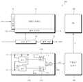
도 2는 본 발명의 제1실시예에 따른 전압 글리치 검출회로를 구비하는 집적회로를 나타낸다. 도 2를 참조하면, 상기 집적회로(100)는 메모리 어레이(12), 로우 디코더(14), 컬럼 디코더(16), 감지 증폭기(18), 출력버퍼(20), 전압 글리치 검출회로(110), 리셋신호 발생기(130), 및 CPU(150)을 구비한다. 본 발명에 따른 집적회로(100)는 스마트 카드 또는 집적회로 카드에 장착될 수 있다.2 shows an integrated circuit having a voltage glitch detection circuit according to a first embodiment of the present invention. Referring to FIG. 2, the
전압 글리치 검출회로(110)는 모니터링 감지 증폭기(113)가 독출한 디지털 데이터와 기준 데이터 저장회로(115)에 저장되어 있는 디지털 데이터를 비교하고, 그 비교결과에 기초하여 감지 증폭기(18)와 상기 모니터링 감지 증폭기(113)로 공급되는 내부전압(VDD)에 발생되는 글리치를 검출한다.The voltage
상기 전압 글리치 검출회로(110)는 모니터링 메모리 어레이(111), 모니터링 감지증폭기(113), 기준 데이터 저장회로(115), 및 비교회로(117)를 구비한다.The voltage
상기 모니터링 메모리 어레이(111)는 적어도 하나의 메모리 셀을 구비하며, 상기 적어도 하나의 메모리 셀의 전기적 특성은 메모리 어레이(12)를 구성하는 다수의 메모리 셀들 각각의 전기적 특성과 동일한 것이 바람직하다. 그리고, 상기 적어도 하나의 메모리 셀은 EEPROM 셀 또는 플레쉬 메모리 셀과 같은 비휘발성 메모리 셀로 구현된다.The
또한, 상기 모니터링 메모리 어레이(111)는 데이터 저장회로로서, 메모리 어레이(12)를 구성하는 각 메모리 셀에 흐르는 전류를 모델링한 소자, 예컨대 저항으로 구현될 수 있다.In addition, the
상기 모니터링 감지증폭기(113)는 감지 증폭기(18)의 독출 동작을 모니터링하기 위한 증폭기로서, 상기 감지 증폭기(18)의 특성과 실질적으로 동일한 특성을 갖는다. 또한, 상기 모니터링 감지증폭기(113)는 상기 감지 증폭기(18)가 메모리 어레이(12)로부터 데이터를 독출하는 타이밍과 동일한 타이밍으로 상기 모니터링 메모리 어레이(111)에 저장된 데이터를 감지 증폭한다. 내부전압(VDD)은 상기 감지 증폭기(18)와 상기 모니터링 감지증폭기(113)로 공급된다.The
상기 기준 데이터 저장회로(115)는 레지스터로 구현될 수 있으며, 적어도 하나의 래치(예컨대, D 플립-플롭)로 구현된다. 상기 기준 데이터 저장회로(115)는 클락신호(CLK)에 응답하여 기준 디지털 데이터를 저장한다.The reference
상기 비교회로(117)는 상기 모니터링 감지증폭기(113)로부터 출력된 로우 레벨로 설정되거나 또는 하이 레벨로 설정된 데이터와 상기 기준 데이터 저장회로(115)로부터 출력된 데이터를 수신하고, 이들을 비교하고, 그 비교결과에 따른 검출신호(DET)를 출력한다. 상기 비교회로(117)는 모니터링 감지증폭기(113)의 출력단자에 접속된 제1입력단자, 상기 기준 데이터 저장회로(115)의 출력단에 접속된 제2입력단자, 및 검출신호(DET)를 출력하는 출력단자를 구비하는 배타 논리합 게이트(119)로 구현될 수 있으나 이에 한정되는 것은 아니다.The
상기 리셋신호 발생기(130)는 상기 비교회로(117)로부터 출력된 검출신호 (DET)에 응답하여 리셋신호(RST)를 발생한다. 집적회로(100)의 동작을 제어하는 상기 CPU(150)는 리셋신호(RST)에 응답하여 리셋된다.The
도 3은 본 발명의 제1실시예에 따른 전압 글리치 검출회로를 구비하는 집적회로의 동작을 나타내는 흐름도이다. 도 2와 도 3을 참조하여 본 발명에 따른 집적회로의 동작을 설명하면 다음과 같다.3 is a flowchart illustrating the operation of an integrated circuit including a voltage glitch detection circuit according to a first embodiment of the present invention. The operation of the integrated circuit according to the present invention will be described with reference to FIGS. 2 and 3 as follows.
집적회로(100)로 소정의 전원이 인가되면, 다수의 래치들로 구현된 상기 기준 데이터 저장회로(115)는 클락신호(CLK)에 응답하여 초기화된다. 즉, 상기 기준 데이터 저장회로(115)는 상기 클락신호(CLK)에 응답하여 기준 데이터(예컨대, 01001100)를 저장한다.When a predetermined power is applied to the
상기 모니터링 메모리 어레이(111)에는 상기 기준 데이터 저장회로(115)에 저장된 기준 데이터(예컨대, 01001100)와 동일한 데이터(예컨대, 01001100)가 저장되어 있다고 가정한다.It is assumed that the
독출 동작시 마다, 감지 증폭기(18)는, 동작 제어신호(OCS)에 응답하여, 로우 어드레스(XADD)와 컬럼 어드레스(YADD)에 기초하여 로우 디코더(14)와 컬럼 디코도(16)에 의하여 지정된 메모리 어레이(12)의 영역에 저장된 데이터(0 또는 1)를 감지하고, 증폭하고, 상기 영역에 저장된 데이터(0 또는 1)에 따라 로우 레벨 또는 하이 레벨로 설정된 데이터를 출력한다.In each read operation, the
상기 독출 동작시 마다, 상기 모니터링 감지증폭기(113)는, 동작 제어신호(OCS)에 응답하여, 모니터링 메모리 어레이(111)에 저장된 데이터(예컨대, 01001100)를 감지하고, 증폭하고, 로우 레벨 또는 하이 레벨로 설정된 데이터를 출 력한다(S110). 그리고, 비교회로(117)는 상기 모니터링 감지증폭기(113)로부터 출력된 데이터(예컨대, 01001100)와 기준 데이터 저장회로(115)에 저장된 데이터(예컨대, 01001100)를 수신하고, 이들을 비교하고(S120), 그 비교결과에 따른 감지신호(DET)를 출력한다.In each read operation, the
상기 모니터링 감지증폭기(113)로 공급되는 내부전압(VDD)에 글리치가 발생되거나, 또는 잡음 등에 의하여 상기 내부전압(VDD)이 안정적이지 못할 경우, 상기 모니터링 감지증폭기(113)는 모니터링 메모리 어레이(111)에 저장된 데이터(예컨대, 01001100)를 정확하게 증폭하지 못한다. 따라서 상기 모니터링 감지증폭기(113)가 상기 모니터링 메모리 어레이(111)로부터 독출한 데이터가 11001100인 경우, 비교회로(117)는 하이 레벨(또는 1)을 갖는 검출신호(DET)를 출력한다(S140). 즉, 상기 모니터링 감지증폭기(113)에서는 독출 실패가 발생한다.When a glitch is generated in the internal voltage VDD supplied to the
리셋신호 발생기(130)는 하이 레벨을 갖는 검출신호(DET)에 응답하여 하이 레벨을 갖는 리셋신호(RST)를 발생한다. 따라서 CPU(150)는 하이 레벨을 갖는 리셋신호(RST)에 응답하여 리셋되므로, 상기 CPU(150)는 더 이상 메모리 어레이(12)를 억세스할 수 없다(S150). 따라서 메모리 어레이(12)에 저장된 데이터는 공격자로부터 안전하게 보호된다.The
그러나, 상기 모니터링 감지증폭기(113)로 공급되는 내부전압(VDD)에 글리치가 발생되지 않거나, 또는 잡음 등에 불구하고 상기 내부전압(VDD)이 안정적인 경우, 상기 모니터링 감지증폭기(113)는 상기 모니터링 메모리 어레이(111)로부터 01001100인 데이터를 독출할 수 있으므로, 비교회로(117)는 로우 레벨(또는 0)을 갖는 검출신호(DET)를 출력한다.However, when glitches are not generated in the internal voltage VDD supplied to the
이때, 리셋신호 발생기(130)는 로우 레벨을 갖는 검출신호(DET)에 응답하여 로우 레벨을 갖는 리셋신호(RST)를 발생한다. 따라서 CPU(150)는 로우 레벨을 갖는 리셋신호(RST)에 응답하여 정상적으로 메모리 어레이(12)를 억세스할 수 있다(S130). 즉, 감지 증폭기(18)는 CPU(150)의 제어하에 정상적인 독출 동작을 수행한다.At this time, the
공격자가 집적회로(100)로 공급되는 외부전압을 비정상 상태로 만드는 경우, 상기 외부전압에 연관된 내부전압(VDD)도 비정상 상태로 된다. 즉, 상기 모니터링 감지증폭기(113)로 공급되는 내부전압(VDD)의 불안정으로 인하여 상기 모니터링 감지증폭기(113)에서 독출 실패가 발생되는 경우, 상기 모니터링 감지증폭기(113)의 특성과 동일한 특성을 갖는 감지 증폭기(18)로 공급되는 내부전압(VDD)도 불안정할 것이다.When the attacker makes the external voltage supplied to the
도 4는 본 발명의 제2실시예에 따른 전압 글리치 검출회로를 구비하는 집적회로를 나타낸다. 도 2와 도 4를 참조하면, 도 4에 도시된 집적회로(200)의 구조와 동작은 전압 글리치 검출회로(210)를 제외하고 도 2에 도시된 집적회로(100)의 구조와 동작과 동일하다.4 shows an integrated circuit having a voltage glitch detection circuit according to a second embodiment of the present invention. 2 and 4, the structure and operation of the
상기 전압 글리치 검출회로(210)는 외부전압(VCC)으로 동작하는 래치(211과 217)로부터 출력된 데이터와 내부전압(VDD)을 비교하고, 비교결과에 따른 검출신호(DET)를 발생한다. 즉, 상기 검출신호(DET)의 레벨은 외부전압(VCC)의 안정성을 판단하는 기준이 된다.The voltage
상기 전압 글리치 검출회로(210)는 제1래치(211), 제1비교회로(213), 제2래치(217), 제2비교회로(219), 및 논리합 게이트(223)를 구비한다.The voltage
상기 제1래치(211)는 외부전압(VCC)이 정상적인 레벨을 갖는 경우 클락신호(CLK)에 응답하여 상기 외부전압(VCC)의 레벨을 갖는 신호(또는 데이터)를 래치한다. 그러나, 외부전압(VCC)이 글리치 또는 잡음 등에 의하여 비정상적인 레벨(예컨대, 순간적으로 접지전압(VSS))을 갖는 경우, 제1래치(211)는 로우 레벨(또는 "0")을 갖는 데이터를 래치할 수 있다.The
상기 제1비교회로(213)는 제1래치(211)의 출력 신호와 내부전압(VDD)을 수신하고, 이들을 비교하고, 비교결과에 따른 검출신호(DET1)를 출력한다. 상기 제1비교회로(213)는 상기 내부전압(VDD)을 수신하는 제1입력단자, 상기 제1래치(211)의 출력 신호를 래치하는 제2입력단자, 및 상기 검출신호(DET1)를 출력하는 출력단자를 구비하는 배타 논리합 게이트(215)로 구현될 수 있으나 이에 한정되는 것은 아니다. 예컨대, 상기 제1비교회로(213)는 외부전압(VCC)이 정상적인 레벨을 갖는 경우 로우 레벨을 갖는 검출신호(DET1)를 출력하나, 상기 외부전압(VCC)이 비정상적인 레벨을 갖는 경우 하이 레벨을 갖는 검출신호(DET1)를 출력한다.The
상기 제2래치(217)는 외부전압(VCC)이 정상적인 레벨을 갖는 경우 클락신호(CLK)에 응답하여 접지전압(VSS)의 레벨을 갖는 신호(또는 데이터)를 래치한다. 그러나, 외부전압(VCC)이 글리치 또는 잡음 등에 의하여 비정상적인 레벨(예컨대, 순간적으로 접지전압(VSS))을 갖는 경우 제2래치(217)는 하이 레벨(또는 "1")을 갖는 데이터를 래치할 수 있다.The
상기 제2비교회로(219)는 제2래치(211)의 출력 신호와 접지전압(VSS)을 수신하고, 이들을 비교하고, 비교결과에 따른 검출신호(DET2)를 출력한다. 상기 제2비교회로(219)는 배타 논리합 게이트(221)로 구현될 수 있으나 이에 한정되는 것은 아니다.The
예컨대, 상기 제2비교회로(219)는 외부전압(VCC)이 정상적인 레벨을 갖는 경우 로우 레벨을 갖는 검출신호(DET2)를 출력하나, 상기 외부전압(VCC)이 비정상적인 레벨을 갖는 경우 하이 레벨을 갖는 검출신호(DET2)를 출력한다.For example, the
상기 논리합 게이트(223)는 제1비교회로(213)와 제2비교회로(219)의 출력신호들(DET1과 DET2)을 수신하고, 이들을 논리합하고, 그 결과에 따른 검출신호(DET)를 출력한다. 상기 논리합 게이트(223)는 외부전압(VCC)이 정상적인 레벨을 갖는 경우 로우 레벨을 갖는 검출신호(DET)를 출력하나, 상기 외부전압(VCC)이 비정상적인 레벨을 갖는 경우 하이 레벨을 갖는 검출신호(DET)를 출력한다.The OR
도 5는 본 발명의 제2실시예에 따른 전압 글리치 검출회로를 구비하는 집적회로의 동작을 나타내는 흐름도이다. 도 4와 도 5를 참조하여 본 발명에 따른 집적회로의 동작을 설명하면 다음과 같다.5 is a flowchart illustrating the operation of an integrated circuit including a voltage glitch detection circuit according to a second embodiment of the present invention. The operation of the integrated circuit according to the present invention will be described with reference to FIGS. 4 and 5 as follows.
대응되는 래치(211과 217)는 클락신호(CLK)에 응답하여 외부전압(VCC)의 레벨을 갖는 데이터 또는 접지전압(VSS)의 레벨을 갖는 데이터를 래치한다(S210). 대응되는 래치(211과 217)는 외부전압(VCC)이 정상적인 레벨을 갖는 경우 대응되는 입력신호(VSS 또는 VSS)의 레벨을 갖는 데이터를 래치하나, 상기 외부전압(VCC)이 글리치 또는 잡음 등에 의하여 비정상적인 레벨을 갖는 경우 상기 대응되는 래치 (211과 217)는 상기 입력신호(VCC 또는 VSS)의 레벨과 다른 레벨(VSS 또는 VCC)을 갖는 데이터를 래치한다.The corresponding latches 211 and 217 latch data having the level of the external voltage VCC or data having the level of the ground voltage VSS in response to the clock signal CLK(S210) . The corresponding latches 211 and 217 latch the data having the level of the corresponding input signal VSS or VSS when the external voltage VCC has a normal level, but the external voltage VCC is caused by a glitch or noise. When the level is abnormal, the corresponding
대응되는 비교회로(213과 219)는 내부전압(VDD 또는 VSS)의 레벨과 대응되는 래치(211과 217)에 의하여 래치된 데이터의 레벨을 비교하고, 그 비교결과에 따른 대응되는 검출신호(DET1과 DET2)를 출력한다(S220).The
외부전압(VCC)이 정상적인 레벨을 갖는 경우, 대응되는 비교회로(213과 219)는 로우 레벨을 갖는 대응되는 검출신호(DET1과 DET2)를 출력하므로 전압 글리치 검출회로(210)는 로우 레벨을 갖는 검출신호(DET)를 출력한다.When the external voltage VCC has a normal level, the
리셋신호 발생기(130)는 로우 레벨을 갖는 검출신호(DET)에 응답하여 로우 레벨을 갖는 리셋신호(RST)를 발생한다. 따라서 CPU(150)는 로우 레벨을 갖는 리셋신호(RST)에 응답하여 정상적으로 메모리 어레이(12)를 억세스할 수 있다(S230).The
그러나, 글리치 또는 잡음 등에 의하여 상기 외부전압(VCC)이 비정상적인 레벨을 갖는 경우, 비교회로들(213과 219) 중에서 적어도 하나는 하이 레벨을 갖는 검출신호(DET1 및/또는 DET2)를 출력하므로 전압 글리치 검출회로(210)는 하이 레벨을 갖는 검출신호(DET)를 출력한다.However, when the external voltage VCC has an abnormal level due to glitch or noise, at least one of the
리셋신호 발생기(130)는 하이 레벨을 갖는 검출신호(DET)에 응답하여 하이 레벨을 갖는 리셋신호(RST)를 발생한다(S240). 따라서 CPU(150)는 하이 레벨을 갖는 리셋신호(RST)에 응답하여 리셋되므로, 상기 CPU(150)는 더 이상 메모리 어레이(12)를 억세스할 수 없다(S250).The
도 6은 본 발명의 제3실시예에 따른 전압 글리치 검출회로를 나타낸다. 도 6 을 참조하면, 전압 글리치 검출회로(310)는 모니터링 메모리 어레이(111), 모니터링 감지증폭기(113), 기준 데이터 저장회로(115), 비교회로(117), 제1래치(211), 제1비교회로(213), 제2래치(217), 제2비교회로(219), 및 논리합 게이트(311)를 구비한다.6 shows a voltage glitch detection circuit according to a third embodiment of the present invention. Referring to FIG. 6, the voltage
상기 전압 글리치 검출회로(310)는 도 2와 도 3을 참조하여 상세히 설명한 바와 같이 감지 증폭기(18)로 공급되는 비정상적인 내부전압(VDD)에 따른 감지 증폭기(18)의 독출 동작을 모니터링하여 검출신호(DET1)를 출력하거나, 또는 도 4와 도5를 참조하여 상세히 설명한 바와 같이 대응되는 래치(211과 217)로 공급되는 비정상적인 외부전압(VCC)의 변동을 모니터링하고 대응되는 검출신호(DET2와 DET3)를 출력하고, 비정상적인 외부전압(VCC)의 변동과 비정상 적인 내부전압(VDD)의 변동 중에서 적어도 하나를 검출하고, 그 검출 결과(DET)를 출력한다.The voltage
도 7은 본 발명의 제3실시예에 따른 전압 글리치 검출회로를 구비하는 집적회로를 나타낸다. 도 7에 도시된 집적회로(300)는 메모리 어레이(12), 로우 디코더(14), 컬럼 디코더(16), 감지 증폭기(18), 출력버퍼(20), 전압 글리치 검출회로(310), 리셋신호 발생기(130), 및 CPU(150)를 구비한다.7 illustrates an integrated circuit including a voltage glitch detection circuit according to a third embodiment of the present invention. The
상기 전압 글리치 검출회로(310)가 비정상 동작 조건, 예컨대 비정상적인 내부전압(VDD) 또는 비정상적인 외부전압(VCC)을 검출한 결과로서 하이 레벨을 갖는 검출신호(DET)를 출력하는 경우, 리셋신호 발생기(130)는 하이 레벨을 갖는 리셋신호(RST)를 CPU(130)로 출력한다. 집적회로(300)의 동작을 제어하는 상기 CPU(130)는 하이 레벨을 갖는 리셋신호(RST)에 응답하여 리셋된다.When the voltage
본 발명은 도면에 도시된 일 실시 예를 참고로 설명되었으나 이는 예시적인 것에 불과하며, 본 기술 분야의 통상의 지식을 가진 자라면 이로부터 다양한 변형 및 균등한 타 실시예가 가능하다는 점을 이해할 것이다. 따라서, 본 발명의 진정한 기술적 보호 범위는 첨부된 등록청구범위의 기술적 사상에 의해 정해져야 할 것이다.Although the present invention has been described with reference to one embodiment shown in the drawings, this is merely exemplary, and those skilled in the art will understand that various modifications and equivalent other embodiments are possible therefrom. Therefore, the true technical protection scope of the present invention will be defined by the technical spirit of the appended claims.
상술한 바와 같이 본 발명에 따른 전압 글리치 검출회로는 모니터링 감지 증폭기를 이용하여 감지 증폭기로 공급되는 불안정한 또는 비정상적인 내부전압을 용이하게 모니터링할 수 있는 이점이 있다.As described above, the voltage glitch detection circuit according to the present invention has an advantage of easily monitoring an unstable or abnormal internal voltage supplied to the sense amplifier by using the monitoring sense amplifier.
상술한 바와 같이 본 발명에 따른 전압 글리치 검출회로는 외부전압을 동작전압으로 하는 래치의 데이터 레벨과 내부 전압을 비교하고, 그 비교결과에 따라 상기 외부전압의 비정상 여부를 용이하게 검출할 수 있는 이점이 있다.As described above, the voltage glitch detection circuit according to the present invention compares the data level of the latch with the external voltage as the operating voltage and the internal voltage, and can easily detect whether the external voltage is abnormal according to the comparison result. There is this.
상술한 바와 같이 CPU와 본 발명에 따른 전압 글리치 검출회로를 구비하는 집적회로는 상기 집적회로로 공급되는 비정상적인 내부전압 또는 비정상적인 외부전압을 검출하고 검출 결과에 기초하여 상기 CPU를 리셋시킬 수 있으므로 상기 집적회로에 저장된 데이터의 보안성이 증가하는 이점이 있다.As described above, an integrated circuit having a CPU and a voltage glitch detection circuit according to the present invention can detect an abnormal internal voltage or an abnormal external voltage supplied to the integrated circuit and reset the CPU based on a detection result. There is an advantage that the security of the data stored in the circuit is increased.
Claims (15)
Translated fromKoreanPriority Applications (6)
| Application Number | Priority Date | Filing Date | Title |
|---|---|---|---|
| KR1020050083498AKR100618051B1 (en) | 2005-09-08 | 2005-09-08 | Apparatus and method for detecting voltage glitches |
| US11/434,933US7483328B2 (en) | 2005-09-08 | 2006-05-17 | Voltage glitch detection circuits and methods thereof |
| TW095121175ATWI315408B (en) | 2005-09-08 | 2006-06-14 | Integrated circuit, voltage glitch detection circuits and methods thereof |
| FR0652959AFR2891943B1 (en) | 2005-09-08 | 2006-07-13 | METHOD AND CIRCUIT FOR DETECTING TRANSIENT VOLTAGE |
| DE102006034271ADE102006034271B4 (en) | 2005-09-08 | 2006-07-18 | Voltage perturbation detection circuit, associated integrated circuit and control method |
| JP2006225637AJP4554573B2 (en) | 2005-09-08 | 2006-08-22 | Voltage glitch detection circuit and detection method thereof |
Applications Claiming Priority (1)
| Application Number | Priority Date | Filing Date | Title |
|---|---|---|---|
| KR1020050083498AKR100618051B1 (en) | 2005-09-08 | 2005-09-08 | Apparatus and method for detecting voltage glitches |
Publications (1)
| Publication Number | Publication Date |
|---|---|
| KR100618051B1true KR100618051B1 (en) | 2006-08-30 |
Family
ID=37601329
Family Applications (1)
| Application Number | Title | Priority Date | Filing Date |
|---|---|---|---|
| KR1020050083498AExpired - LifetimeKR100618051B1 (en) | 2005-09-08 | 2005-09-08 | Apparatus and method for detecting voltage glitches |
Country Status (6)
| Country | Link |
|---|---|
| US (1) | US7483328B2 (en) |
| JP (1) | JP4554573B2 (en) |
| KR (1) | KR100618051B1 (en) |
| DE (1) | DE102006034271B4 (en) |
| FR (1) | FR2891943B1 (en) |
| TW (1) | TWI315408B (en) |
Cited By (1)
| Publication number | Priority date | Publication date | Assignee | Title |
|---|---|---|---|---|
| KR102188138B1 (en)* | 2020-03-05 | 2020-12-07 | 주식회사 로제타텍 | Fire alarm apparatus |
Families Citing this family (15)
| Publication number | Priority date | Publication date | Assignee | Title |
|---|---|---|---|---|
| US20080086781A1 (en)* | 2006-10-06 | 2008-04-10 | Stephane Rodgers | Method and system for glitch protection in a secure system |
| KR100837275B1 (en)* | 2006-12-06 | 2008-06-11 | 삼성전자주식회사 | Smart card to detect light |
| WO2009034490A1 (en)* | 2007-09-10 | 2009-03-19 | Nxp B.V. | Integrated circuit with data line monitoring and alarm signal |
| GB2508172A (en)* | 2012-11-22 | 2014-05-28 | St Microelectronics Res & Dev | A power-on reset signal generator which can detect short transient dips in the power supply voltage |
| US8892903B1 (en)* | 2012-12-06 | 2014-11-18 | Xilinx, Inc. | Detection of power analysis attacks |
| GB2510129B (en)* | 2013-01-24 | 2015-06-10 | Nds Ltd | Passing hidden information using attack detectors |
| KR102081923B1 (en)* | 2013-02-04 | 2020-02-26 | 삼성전자주식회사 | Memory system and operating method of meomry controller |
| US10302698B1 (en)* | 2017-05-08 | 2019-05-28 | Xilinx, Inc. | Estimation of power consumed by combinatorial circuitry |
| US10733327B2 (en) | 2018-06-26 | 2020-08-04 | Taiwan Semiconductor Manufacturing Co., Ltd. | Method and apparatus for protecting a PUF generator |
| US10466275B1 (en)* | 2018-06-28 | 2019-11-05 | Xilinx, Inc. | Glitch detector and test glitch generator |
| US11164648B2 (en) | 2019-06-18 | 2021-11-02 | Nxp Usa, Inc. | Glitch profiling in an integrated circuit |
| US11855641B2 (en) | 2020-07-07 | 2023-12-26 | Infineon Technologies LLC | Integrated resistor network and method for fabricating the same |
| KR102834966B1 (en) | 2020-10-30 | 2025-07-16 | 삼성전자주식회사 | Glitch detector, security device including the same and electronic device including the same |
| US11977664B2 (en)* | 2021-11-19 | 2024-05-07 | Nxp Usa, Inc. | Supply voltage proportionality monitoring in a system-on-chip (SOC) |
| US12068050B2 (en) | 2022-06-02 | 2024-08-20 | Micron Technology, Inc. | Glitch detection redundancy |
Citations (3)
| Publication number | Priority date | Publication date | Assignee | Title |
|---|---|---|---|---|
| JPH11317096A (en) | 1998-02-06 | 1999-11-16 | Samsung Electronics Co Ltd | Self-test circuit for composite semiconductor memory device and self-test method using the same |
| KR20030092777A (en)* | 2002-05-31 | 2003-12-06 | 삼성전자주식회사 | Circuit For Detecting A Volatage Glitch, An Integrated Circuit Device Having The Same, And An Apparatus And Method For Securing An Integrated Circuit Device From A Voltage Glitch Attack |
| JP2004030887A (en) | 2002-05-29 | 2004-01-29 | Agilent Technol Inc | Integrated circuit including FeRAM cell and test method therefor |
Family Cites Families (10)
| Publication number | Priority date | Publication date | Assignee | Title |
|---|---|---|---|---|
| US6085342A (en)* | 1997-05-06 | 2000-07-04 | Telefonaktiebolaget L M Ericsson (Publ) | Electronic system having a chip integrated power-on reset circuit with glitch sensor |
| JP4231572B2 (en)* | 1998-07-07 | 2009-03-04 | 沖電気工業株式会社 | Voltage monitoring circuit and memory card incorporating the same |
| JP2000076139A (en)* | 1998-08-28 | 2000-03-14 | Nippon Telegr & Teleph Corp <Ntt> | Portable information storage medium |
| US6161213A (en)* | 1999-02-17 | 2000-12-12 | Icid, Llc | System for providing an integrated circuit with a unique identification |
| EP1154375A1 (en) | 2000-05-11 | 2001-11-14 | Infineon Technologies AG | Circuit for detection of external influences on a semiconductor chip |
| JP3827534B2 (en)* | 2001-03-01 | 2006-09-27 | シャープ株式会社 | Reference voltage generating circuit and memory reading circuit for semiconductor memory device |
| DE10162306A1 (en) | 2001-12-19 | 2003-07-03 | Philips Intellectual Property | Method and arrangement for verifying NV fuses as well as a corresponding computer program product and a corresponding computer-readable storage medium |
| KR100476892B1 (en) | 2002-04-29 | 2005-03-17 | 삼성전자주식회사 | Tamper-resistant method and data processing system using the same |
| JP4124692B2 (en)* | 2003-04-25 | 2008-07-23 | シャープ株式会社 | Nonvolatile semiconductor memory device |
| JP4322686B2 (en) | 2004-01-07 | 2009-09-02 | 株式会社東芝 | Nonvolatile semiconductor memory device |
- 2005
- 2005-09-08KRKR1020050083498Apatent/KR100618051B1/ennot_activeExpired - Lifetime
- 2006
- 2006-05-17USUS11/434,933patent/US7483328B2/enactiveActive
- 2006-06-14TWTW095121175Apatent/TWI315408B/enactive
- 2006-07-13FRFR0652959Apatent/FR2891943B1/enactiveActive
- 2006-07-18DEDE102006034271Apatent/DE102006034271B4/enactiveActive
- 2006-08-22JPJP2006225637Apatent/JP4554573B2/enactiveActive
Patent Citations (3)
| Publication number | Priority date | Publication date | Assignee | Title |
|---|---|---|---|---|
| JPH11317096A (en) | 1998-02-06 | 1999-11-16 | Samsung Electronics Co Ltd | Self-test circuit for composite semiconductor memory device and self-test method using the same |
| JP2004030887A (en) | 2002-05-29 | 2004-01-29 | Agilent Technol Inc | Integrated circuit including FeRAM cell and test method therefor |
| KR20030092777A (en)* | 2002-05-31 | 2003-12-06 | 삼성전자주식회사 | Circuit For Detecting A Volatage Glitch, An Integrated Circuit Device Having The Same, And An Apparatus And Method For Securing An Integrated Circuit Device From A Voltage Glitch Attack |
Cited By (2)
| Publication number | Priority date | Publication date | Assignee | Title |
|---|---|---|---|---|
| KR102188138B1 (en)* | 2020-03-05 | 2020-12-07 | 주식회사 로제타텍 | Fire alarm apparatus |
| US12183185B2 (en) | 2020-03-05 | 2024-12-31 | Rozetatech Co., Ltd. | Fire alarm apparatus |
Also Published As
| Publication number | Publication date |
|---|---|
| JP4554573B2 (en) | 2010-09-29 |
| TWI315408B (en) | 2009-10-01 |
| FR2891943B1 (en) | 2012-01-13 |
| TW200710419A (en) | 2007-03-16 |
| FR2891943A1 (en) | 2007-04-13 |
| US20070058452A1 (en) | 2007-03-15 |
| US7483328B2 (en) | 2009-01-27 |
| DE102006034271A1 (en) | 2007-03-22 |
| DE102006034271B4 (en) | 2008-10-02 |
| JP2007073041A (en) | 2007-03-22 |
Similar Documents
| Publication | Publication Date | Title |
|---|---|---|
| JP4554573B2 (en) | Voltage glitch detection circuit and detection method thereof | |
| US7535744B2 (en) | Semiconductor integrated circuit and IC card system having internal information protection | |
| US7969763B2 (en) | Detector circuit for detecting an external manipulation of an electrical circuit, circuit arrangement comprising a plurality of detector circuits, memory device and method for operating a detector circuit | |
| US5875142A (en) | Integrated circuit with temperature detector | |
| KR100591026B1 (en) | Integrated Circuit Memory with Fuse Detection Circuit | |
| US6201742B1 (en) | Circuit that prevents illegal transformation of data in a non-volatile memory and a method for the same | |
| US7916517B2 (en) | Circuit arrangement and method for recognizing manipulation attempts | |
| KR20090036182A (en) | Memory device capable of detecting light attack and its method | |
| KR20110010733A (en) | Secure random number generator | |
| US20070019473A1 (en) | Apparatus and method for improving write/read endurance of non-volatile memory | |
| US20100169752A1 (en) | Storage circuit with fault detection and method for operating the same | |
| CN106683703B (en) | Data reading method, integrated circuit and chip | |
| US20250167139A1 (en) | Laser detecting circuit and semiconductor apparatus including the same | |
| US7450451B2 (en) | Nonvolatile memory system and method for controlling nonvolatile memory | |
| KR20050046520A (en) | Memory system having flash memory where otp block is included | |
| US6456539B1 (en) | Method and apparatus for sensing a memory signal from a selected memory cell of a memory device | |
| US12040004B2 (en) | Storage device with counter | |
| KR100830584B1 (en) | Flash memory device and smart card including it | |
| US7787315B2 (en) | Semiconductor device and method for detecting abnormal operation | |
| US7139186B2 (en) | Failure detection circuit | |
| US6751139B2 (en) | Integrated circuit reset circuitry | |
| US7710762B2 (en) | Device for protecting SRAM data | |
| US20240354449A1 (en) | Glitch detector and glitch detection method using the same | |
| US12189541B1 (en) | Memory device and control method for controlling memory device | |
| US11700003B2 (en) | Microcontroller, operation system and control method thereof |
Legal Events
| Date | Code | Title | Description |
|---|---|---|---|
| A201 | Request for examination | ||
| PA0109 | Patent application | Patent event code:PA01091R01D Comment text:Patent Application Patent event date:20050908 | |
| PA0201 | Request for examination | ||
| E701 | Decision to grant or registration of patent right | ||
| PE0701 | Decision of registration | Patent event code:PE07011S01D Comment text:Decision to Grant Registration Patent event date:20060818 | |
| GRNT | Written decision to grant | ||
| PR0701 | Registration of establishment | Comment text:Registration of Establishment Patent event date:20060823 Patent event code:PR07011E01D | |
| PR1002 | Payment of registration fee | Payment date:20060824 End annual number:3 Start annual number:1 | |
| PG1601 | Publication of registration | ||
| PR1001 | Payment of annual fee | Payment date:20090814 Start annual number:4 End annual number:4 | |
| PR1001 | Payment of annual fee | Payment date:20100729 Start annual number:5 End annual number:5 | |
| PR1001 | Payment of annual fee | Payment date:20110729 Start annual number:6 End annual number:6 | |
| FPAY | Annual fee payment | Payment date:20120801 Year of fee payment:7 | |
| PR1001 | Payment of annual fee | Payment date:20120801 Start annual number:7 End annual number:7 | |
| FPAY | Annual fee payment | Payment date:20130731 Year of fee payment:8 | |
| PR1001 | Payment of annual fee | Payment date:20130731 Start annual number:8 End annual number:8 | |
| FPAY | Annual fee payment | Payment date:20140731 Year of fee payment:9 | |
| PR1001 | Payment of annual fee | Payment date:20140731 Start annual number:9 End annual number:9 | |
| FPAY | Annual fee payment | Payment date:20160801 Year of fee payment:11 | |
| PR1001 | Payment of annual fee | Payment date:20160801 Start annual number:11 End annual number:11 | |
| FPAY | Annual fee payment | Payment date:20180731 Year of fee payment:13 | |
| PR1001 | Payment of annual fee | Payment date:20180731 Start annual number:13 End annual number:13 | |
| PR1001 | Payment of annual fee | Payment date:20200731 Start annual number:15 End annual number:15 | |
| PR1001 | Payment of annual fee | Payment date:20210728 Start annual number:16 End annual number:16 | |
| PR1001 | Payment of annual fee | Payment date:20220727 Start annual number:17 End annual number:17 | |
| PR1001 | Payment of annual fee | Payment date:20230801 Start annual number:18 End annual number:18 | |
| PR1001 | Payment of annual fee | Payment date:20240729 Start annual number:19 End annual number:19 |