KR100617883B1 - Thin film deposition method using ECDTMD - Google Patents
Thin film deposition method using ECDTMDDownload PDFInfo
- Publication number
- KR100617883B1 KR100617883B1KR1020050003196AKR20050003196AKR100617883B1KR 100617883 B1KR100617883 B1KR 100617883B1KR 1020050003196 AKR1020050003196 AKR 1020050003196AKR 20050003196 AKR20050003196 AKR 20050003196AKR 100617883 B1KR100617883 B1KR 100617883B1
- Authority
- KR
- South Korea
- Prior art keywords
- thin film
- reactant
- chamber
- film deposition
- depositing
- Prior art date
- Legal status (The legal status is an assumption and is not a legal conclusion. Google has not performed a legal analysis and makes no representation as to the accuracy of the status listed.)
- Expired - Fee Related
Links
Images

Classifications
- H—ELECTRICITY
- H01—ELECTRIC ELEMENTS
- H01L—SEMICONDUCTOR DEVICES NOT COVERED BY CLASS H10
- H01L21/00—Processes or apparatus adapted for the manufacture or treatment of semiconductor or solid state devices or of parts thereof
- H01L21/02—Manufacture or treatment of semiconductor devices or of parts thereof
- H01L21/04—Manufacture or treatment of semiconductor devices or of parts thereof the devices having potential barriers, e.g. a PN junction, depletion layer or carrier concentration layer
- H01L21/18—Manufacture or treatment of semiconductor devices or of parts thereof the devices having potential barriers, e.g. a PN junction, depletion layer or carrier concentration layer the devices having semiconductor bodies comprising elements of Group IV of the Periodic Table or AIIIBV compounds with or without impurities, e.g. doping materials
- H01L21/28—Manufacture of electrodes on semiconductor bodies using processes or apparatus not provided for in groups H01L21/20 - H01L21/268
- H01L21/283—Deposition of conductive or insulating materials for electrodes conducting electric current
- H01L21/285—Deposition of conductive or insulating materials for electrodes conducting electric current from a gas or vapour, e.g. condensation
- H01L21/28506—Deposition of conductive or insulating materials for electrodes conducting electric current from a gas or vapour, e.g. condensation of conductive layers
- H01L21/28512—Deposition of conductive or insulating materials for electrodes conducting electric current from a gas or vapour, e.g. condensation of conductive layers on semiconductor bodies comprising elements of Group IV of the Periodic Table
- H01L21/28556—Deposition of conductive or insulating materials for electrodes conducting electric current from a gas or vapour, e.g. condensation of conductive layers on semiconductor bodies comprising elements of Group IV of the Periodic Table by chemical means, e.g. CVD, LPCVD, PECVD, laser CVD
- C—CHEMISTRY; METALLURGY
- C23—COATING METALLIC MATERIAL; COATING MATERIAL WITH METALLIC MATERIAL; CHEMICAL SURFACE TREATMENT; DIFFUSION TREATMENT OF METALLIC MATERIAL; COATING BY VACUUM EVAPORATION, BY SPUTTERING, BY ION IMPLANTATION OR BY CHEMICAL VAPOUR DEPOSITION, IN GENERAL; INHIBITING CORROSION OF METALLIC MATERIAL OR INCRUSTATION IN GENERAL
- C23C—COATING METALLIC MATERIAL; COATING MATERIAL WITH METALLIC MATERIAL; SURFACE TREATMENT OF METALLIC MATERIAL BY DIFFUSION INTO THE SURFACE, BY CHEMICAL CONVERSION OR SUBSTITUTION; COATING BY VACUUM EVAPORATION, BY SPUTTERING, BY ION IMPLANTATION OR BY CHEMICAL VAPOUR DEPOSITION, IN GENERAL
- C23C16/00—Chemical coating by decomposition of gaseous compounds, without leaving reaction products of surface material in the coating, i.e. chemical vapour deposition [CVD] processes
- C23C16/44—Chemical coating by decomposition of gaseous compounds, without leaving reaction products of surface material in the coating, i.e. chemical vapour deposition [CVD] processes characterised by the method of coating
- C23C16/448—Chemical coating by decomposition of gaseous compounds, without leaving reaction products of surface material in the coating, i.e. chemical vapour deposition [CVD] processes characterised by the method of coating characterised by the method used for generating reactive gas streams, e.g. by evaporation or sublimation of precursor materials
- C23C16/4481—Chemical coating by decomposition of gaseous compounds, without leaving reaction products of surface material in the coating, i.e. chemical vapour deposition [CVD] processes characterised by the method of coating characterised by the method used for generating reactive gas streams, e.g. by evaporation or sublimation of precursor materials by evaporation using carrier gas in contact with the source material
- C23C16/4482—Chemical coating by decomposition of gaseous compounds, without leaving reaction products of surface material in the coating, i.e. chemical vapour deposition [CVD] processes characterised by the method of coating characterised by the method used for generating reactive gas streams, e.g. by evaporation or sublimation of precursor materials by evaporation using carrier gas in contact with the source material by bubbling of carrier gas through liquid source material
- H—ELECTRICITY
- H01—ELECTRIC ELEMENTS
- H01L—SEMICONDUCTOR DEVICES NOT COVERED BY CLASS H10
- H01L21/00—Processes or apparatus adapted for the manufacture or treatment of semiconductor or solid state devices or of parts thereof
- H01L21/02—Manufacture or treatment of semiconductor devices or of parts thereof
- H01L21/02041—Cleaning
- H01L21/02043—Cleaning before device manufacture, i.e. Begin-Of-Line process
- H01L21/02046—Dry cleaning only
- H—ELECTRICITY
- H01—ELECTRIC ELEMENTS
- H01L—SEMICONDUCTOR DEVICES NOT COVERED BY CLASS H10
- H01L21/00—Processes or apparatus adapted for the manufacture or treatment of semiconductor or solid state devices or of parts thereof
- H01L21/02—Manufacture or treatment of semiconductor devices or of parts thereof
- H01L21/02104—Forming layers
- H01L21/02107—Forming insulating materials on a substrate
- H01L21/02109—Forming insulating materials on a substrate characterised by the type of layer, e.g. type of material, porous/non-porous, pre-cursors, mixtures or laminates
- H01L21/02112—Forming insulating materials on a substrate characterised by the type of layer, e.g. type of material, porous/non-porous, pre-cursors, mixtures or laminates characterised by the material of the layer
- H01L21/02172—Forming insulating materials on a substrate characterised by the type of layer, e.g. type of material, porous/non-porous, pre-cursors, mixtures or laminates characterised by the material of the layer the material containing at least one metal element, e.g. metal oxides, metal nitrides, metal oxynitrides or metal carbides
- H01L21/02175—Forming insulating materials on a substrate characterised by the type of layer, e.g. type of material, porous/non-porous, pre-cursors, mixtures or laminates characterised by the material of the layer the material containing at least one metal element, e.g. metal oxides, metal nitrides, metal oxynitrides or metal carbides characterised by the metal
- H01L21/02186—Forming insulating materials on a substrate characterised by the type of layer, e.g. type of material, porous/non-porous, pre-cursors, mixtures or laminates characterised by the material of the layer the material containing at least one metal element, e.g. metal oxides, metal nitrides, metal oxynitrides or metal carbides characterised by the metal the material containing titanium, e.g. TiO2
- H—ELECTRICITY
- H01—ELECTRIC ELEMENTS
- H01L—SEMICONDUCTOR DEVICES NOT COVERED BY CLASS H10
- H01L21/00—Processes or apparatus adapted for the manufacture or treatment of semiconductor or solid state devices or of parts thereof
- H01L21/02—Manufacture or treatment of semiconductor devices or of parts thereof
- H01L21/04—Manufacture or treatment of semiconductor devices or of parts thereof the devices having potential barriers, e.g. a PN junction, depletion layer or carrier concentration layer
- H01L21/18—Manufacture or treatment of semiconductor devices or of parts thereof the devices having potential barriers, e.g. a PN junction, depletion layer or carrier concentration layer the devices having semiconductor bodies comprising elements of Group IV of the Periodic Table or AIIIBV compounds with or without impurities, e.g. doping materials
- H01L21/30—Treatment of semiconductor bodies using processes or apparatus not provided for in groups H01L21/20 - H01L21/26
- H01L21/324—Thermal treatment for modifying the properties of semiconductor bodies, e.g. annealing, sintering
Landscapes
- Engineering & Computer Science (AREA)
- Chemical & Material Sciences (AREA)
- Computer Hardware Design (AREA)
- Microelectronics & Electronic Packaging (AREA)
- Power Engineering (AREA)
- Condensed Matter Physics & Semiconductors (AREA)
- General Physics & Mathematics (AREA)
- Manufacturing & Machinery (AREA)
- Physics & Mathematics (AREA)
- Chemical Kinetics & Catalysis (AREA)
- General Chemical & Material Sciences (AREA)
- Materials Engineering (AREA)
- Mechanical Engineering (AREA)
- Metallurgy (AREA)
- Organic Chemistry (AREA)
- Chemical Vapour Deposition (AREA)
- Electrodes Of Semiconductors (AREA)
Abstract
Translated fromKoreanDescription
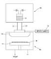
Translated fromKorean도 1은 본 발명에 따른 박막증착방법이 수행되는 박막증착장치의 일 실시예를 도시한 도면,1 is a view showing an embodiment of a thin film deposition apparatus is performed a thin film deposition method according to the present invention,
도 2는 본 발명에 따른 박막증착방법이 수행되는 박막증착장치의 다른 실시예를 도시한 도면.2 is a view showing another embodiment of a thin film deposition apparatus in which the thin film deposition method according to the present invention is performed.
<도면의 주요부분에 대한 부호의 설명><Description of the symbols for the main parts of the drawings>
10 ... 반응기10 ... reactor
11 ... 챔버11 ... chamber
12 ... 서셉터12 ... susceptor
13 ... 샤워헤드13 ... showerhead
20 ... 가스박스20 ... gas box
21 ... 캐니스터21 ... canister
L1, L2, L3 ... 제1,2,3가스라인L1, L2, L3 ... first, second, third gas lines
본 발명은 ECTDMAT(Ethylcyclopentadienyltris(dimethylamino) titanium)을 이용하여 박막을 증착하는 박막증착방법에 관한 것이다.The present invention relates to a thin film deposition method for depositing a thin film using ECTDMAT (Ethylcyclopentadienyltris (dimethylamino) titanium).
현재 대형 소자 업체를 중심으로 커패시터 일렉트로드(capacitor electrode) 및 Al 공정에서의 배리어 머티리얼(barrier material)에 적용하고 있는 TiN 공정에서는 Ti 소스로서 주로 TiCl4을 사용하고 있다. 그러나 TiCl4를 사용하게 되면 Cl 성분이 잔류하게 되는데 Cl은 부식성이 있어 소자의 성능을 저하시킨다.Currently, TiCl4 mainly uses TiCl4 as the Ti source in the TiN process, which is applied to the capacitor electrode and the barrier material in the Al process, mainly among large device makers. However, the use of TiCl4 leaves Cl, which is corrosive and degrades device performance.
따라서 이를 제거하기 위하여 500℃ 이상의 고온 공정을 적용하게 되는데 이것은 또 다른 문제, 즉 TiN 막이 유전재료와 반응하거나 산화되어 커패시터(capacitor)의 전기적 특성을 저하시킬 뿐만 아니라 부식성의 Cl 성분은 배선 공정에의 적용을 제한하는 원인이 된다.Therefore, in order to remove this, a high temperature process of 500 ° C. or more is applied. This is another problem, that is, the TiN film reacts with or oxidizes with the dielectric material, thereby degrading the electrical characteristics of the capacitor. It causes the application to be restricted.
이와 같은 문제점을 해결하고자 400℃ 이하의 저온영역에서 TiN 박막을 형성할 수 있을 뿐만 아니라 Cl 성분을 근원적으로 제거할 수 있는 TDMAT, TEMAT와 같은 유기금속 계열 소스들이 사용되었다.In order to solve this problem, organometallic sources such as TDMAT and TEMAT, which can not only form a TiN thin film in a low temperature region of 400 ° C. or less, but also remove Cl components, are used.
그러나 해당 소스들은 H2O와 쉽게 반응하여 산소에 의한 불순물(oxygen contamination)과 공정 중 파티클 생성이라는 바람직하지 않은 결과를 초래하고 또한 NH3 와의 높은 반응성으로 인하여 공정 파티클을 생성시키며 아미드 알킬 리간드(amide alkyl ligand)에서 비롯된 carbon 성분은 비저항을 높여 결과적으로 소자 성능을 저하시키는 원인이 된다.However, these sources easily react with H2O, which results in undesirable effects such as oxygen contamination and in-process particle formation, and also due to the high reactivity with NH3, it produces process particles and amide alkyl ligands. The carbon component derived from increases the specific resistance, which in turn causes the device performance to degrade.
본 발명은 상기와 같은 문제점을 해결하기 위하여 창출된 것으로서, 로우 아미드 타입(low amide type)의 소스인 ECTDMAT(Ethylcyclo- pentadienyltris(dimethylamino) titanium)을 이용하여 비교적 저온에서 박막증착이 가능하고 막질이 우수한 Ti 함유 박막을 증착하는 박막증착방법을 제공하는 것을 목적으로 한다.The present invention has been made to solve the above problems, using a low amide type (ECTDMAT) (Ethylcyclo- pentadienyltris (dimethylamino) titanium) is a thin film can be deposited at a relatively low temperature and excellent film quality An object of the present invention is to provide a thin film deposition method for depositing a Ti-containing thin film.
상기와 같은 목적을 달성하기 위하여, 본 발명에 따른 박막증착방법의 일 실시예는, 기판상에 Ti 원소를 포함하는 박막을 증착하기 위하여, 제1,2반응물질이 유입되는 반응기 챔버(11) 내의 서셉터 상에 기판을 안착시키는 기판안착단계(S1)와, 상기 기판상에 상기 박막을 증착하기 위한 제1반응물질과 제2반응물질을 상기 기판(w) 상에 분사하여 박막을 증착하는 박막증착단계(S2)를 포함하고, 상기 박막증착단계(S2)는, 제1반응물질로 ECTDMAT (Ethylcyclopentadienyltris(dimethylamino) titanium)을 이용하는 것을 특징으로 한다.In order to achieve the above object, one embodiment of the thin film deposition method according to the present invention, in order to deposit a thin film containing a Ti element on the substrate, the
본 발명에 있어서, 상기 박막증착단계(S2)는, 제1반응물질로서 상기 ECTDMAT를 상기 챔버(11)로 피딩하는 제1피딩단계(S2-1)와, 상기 제1반응물질을 상기 챔버(11)로부터 퍼지하는 제1퍼지단계(S2-2)와, 상기 챔버(11)로 제2반응물질을 피딩하는 제2피딩단계(S2-3)와, 상기 챔버(11)로부터 반응하지 않거나 반응하여 생성된 부산물을 퍼지하는 제2퍼지단계(S2-4)로 구성되는 ALD 싸이클을 반복함으로써 가판(w)상에 박막을 증착한다.In the present invention, the thin film deposition step (S2), the first feeding step (S2-1) for feeding the ECTDMAT as the first reaction material to the
본 발명에 있어서, 상기 박막증착단계(S2)는, 상기 박막증착단계(S2')는, 제1반응물질로서 상기 ECTDMAT를 상기 챔버(11)로 피딩하는 제1피딩단계(S2'-1)와 제2반응물질을 상기 챔버(11)로 피딩하는 제2피딩단계(S2'-3)를 동시에 수행하는 단계와, 불활성가스를 상기 챔버(11)로 유입시켜 박막증착에 사용되지 않은 나머지 가스를 퍼지시키는 퍼지단계를 포함하여 이루어지는 CVD 싸이클을 적어도 1회 이상 반복함으로써 기판(w) 상에 박막을 증착한다.In the present invention, the thin film deposition step (S2), the thin film deposition step (S2 '), the first feeding step (S2'-1) for feeding the ECTDMAT as the first reaction material to the
상기와 같은 목적을 달성하기 위하여, 본 발명에 따른 박막증착방법의 다른 실시예는, 기판상에 Ti 원소를 포함하는 박막을 증착하기 위하여, 제1,2,3반응물질이 유입되는 챔버(11)의 서셉터 상에 기판을 안착시키는 기판안착단계(S1)와, 상기 기판상에 상기 박막을 증착하기 위한 제1반응물질과 제2반응물질과 제3반응물질을 상기 기판(w) 상에 분사하여 박막을 증착하는 박막증착단계(S2)를 포함하고, 상기 박막증착단계(S2)는, 제1반응물질로 ECTDMAT을 이용하는 것을 특징으로 한다.In order to achieve the above object, another embodiment of the thin film deposition method according to the present invention, in order to deposit a thin film containing a Ti element on the substrate, the
본 발명에 있어서, 상기 박막증착단계(S2)는, 제1반응물질로서 상기 ECTDMAT를 상기 챔버(11)로 피딩하는 제1피딩단계(S2-1)와, 상기 제1반응물질을 상기 챔버(11)로부터 퍼지하는 제1퍼지단계(S2-2)와, 상기 챔버(11)로 제2반응물질을 피딩하는 제2피딩단계(S2-3)와, 상기 챔버(11)로부터 반응하지 않거나 반응하여 생성된 부산물을 퍼지하는 제2퍼지단계(S2-4)와, 제3반응물질을 상기 챔버(11)로 피딩하는 제3피딩단계(S2-5)와, 상기 챔버(11)로부터 반응하지 않거나 반응하여 생성된 부산물을 퍼지하는 제3퍼지단계(S2-6)로 구성되는 ALD 싸이클을 반복함으로써 가판(w)상에 박막을 증착한다.In the present invention, the thin film deposition step (S2), the first feeding step (S2-1) for feeding the ECTDMAT as the first reaction material to the
본 발명에 있어서, 상기 박막증착단계(S2')는, 제1반응물질로서 상기 ECTDMAT를 상기 챔버(11)로 피딩하는 제1피딩단계(S2'-1)와 제2반응물질을 상기 챔버(11)로 피딩하는 제2피딩단계(S2'-3)와 제3반응물질을 상기 챔버(11)로 피딩하는 제3피딩단계(S2'-5)를 동시에 수행하는 단계와, 불활성가스를 상기 챔버(11)로 유입시켜 박막증착에 사용되지 않은 나머지 가스를 퍼지시키는 퍼지단계를 포함하여 이루어지는 CVD 싸이클을 적어도 1회 이상 반복함으로써 기판(w) 상에 박막을 증착한다.In the present invention, the thin film deposition step (S2 '), the first feeding step (S2'-1) for feeding the ECTDMAT as the first reaction material to the
상기와 같은 목적을 달성하기 위하여, 본 발명에 따른 박막증착방법의 또 다른 실시예는, 기판상에 Ti 원소를 포함하는 박막을 증착하기 위하여, 반응물질이 유입되는 챔버 내의 서셉터 상에 기판을 안착시키는 기판안착단계(S1)와, 상기 기판상에 상기 박막을 증착하기 위한 반응물질을 상기 기판(w) 상에 분사하여 박막을 증착하는 박막증착단계(S2)를 포함하고, 상기 박막증착단계(S2)는, 반응물질로 ECTDMAT을 이용하고, 상기 챔버(11)로 인가출력이 50w ~ 2000W 의 범위의 플라즈마를 직접 인가하는 다이렉트 플라즈마(direct plasma) 분위기 또는, 외부에서 발생된 인가출력이 50w ~ 2000w 인 플라즈마를 상기 챔버(11) 내로 유도하는 리모트 플라즈마(remote plasma) 분위기에서, 자체 열분해작용에 의하여 Ti 와 TiN 이 혼용된 박막을 증착하는 것을 특징으로 한다.bIn order to achieve the above object, another embodiment of the thin film deposition method according to the present invention, in order to deposit a thin film containing a Ti element on the substrate, the substrate on the susceptor in the chamber into which the reactant is introduced And a thin film deposition step (S2) for depositing a thin film by spraying a reaction material for depositing the thin film on the substrate (W) onto the substrate (W). S2 is a direct plasma atmosphere in which ECTDMAT is used as a reaction material and a plasma having an applied output of 50 w to 2000 W is directly applied to the
이하 첨부된 도면을 참조하면서 본 발명에 따른 박막증착방법을 상세히 설명한다.Hereinafter, a thin film deposition method according to the present invention will be described in detail with reference to the accompanying drawings.
도 1은 본 발명에 따른 박막증착방법이 수행되는 박막증착장치의 일 실시예를 도시한 도면이고, 도 2는 본 발명에 따른 박막증착방법이 수행되는 박막증착장치의 다른 실시예를 도시한 도면이다.1 is a view showing an embodiment of a thin film deposition apparatus is performed a thin film deposition method according to the present invention, Figure 2 is a view showing another embodiment of a thin film deposition apparatus is performed a thin film deposition method according to the present invention to be.
도시된 바와 같이, 본 발명에 따른 박막증착방법이 적용되는 박막증착장치 는, 기판(w)이 수납되는 반응기(10)와, 반응기(10)로 반응물질과 불활성가스를 공급하는 가스박스(20)로 구성된다.As shown, the thin film deposition apparatus to which the thin film deposition method according to the present invention is applied includes a
반응기(10)는, 기판(w)을 안착시키기 위한 서셉터(12)가 내장된 챔버(11)와, 기판(w)을 향하는 다수개의 분사홀이 형성된 샤워헤드(13)와, 플라즈마를 발생하는 플라즈마발생기(RF generator and matching network))를 포함한다. 이때, 서셉터(12)는 안착된 기판(w)을 임의의 온도로 가열한다.The
가스박스(20)는 ECTDMAT(Ethylcyclopentadienyltris(dimethylamino) titanium)가 수용되는 캐니스터(21)와, ECTDMAT를 반응기(10)로 이송하기 위한 이송가스나 반응기(10)를 퍼지하기 위한 퍼지가스의 유량을 제어하는 MFC 등을 포함하고, 캐니스터(21)나 MFC, 또는 반응기(10) 사이의 제1,2가스라인(L1)(L2)등에는 다수개의 밸브(V)가 설치된다. 여기서, 제1가스라인(L1)은 제1반응물질 및/또는 불활성가스가 경유하는 라인이고, 제2가스라인(L2)은 제2반응물질 및/또는 불활성가스가 경유하는 라인으로 정의한다. 그리고, 도 2에 도시된 바와 같이 제3가스라인(L3)을 채용하였을 때 그 제3가스라인(L3)으로는 제3반응물질 및/또는 불활성가스가 경유하게 된다.The
상기한 박막증착장를 이용하여 기판상에 Ti 함유 박막을 증착하는 박막증착방법의 다양한 실시예를 설명한다.Various embodiments of a thin film deposition method for depositing a Ti-containing thin film on a substrate using the thin film deposition site will be described.
먼저, 본 발명에 따른 박막증착방법의 제1실시예를 설명한다. 박막증착방법의 제1실시예는 제1반응물질로서 ECTDMAT를 이용하고, 제1반응물질과 다른 제2반응물질을 이용하며, ALD 방식을 통하여 기판상에 Ti 함유 박막을 증착하는 것이다.First, a first embodiment of a thin film deposition method according to the present invention will be described. The first embodiment of the thin film deposition method uses ECTDMAT as the first reactant, uses a second reactant different from the first reactant, and deposits a Ti-containing thin film on the substrate through an ALD method.
여기서, ECTDMAT 는 기존 TDMAT 의 아미드 알킬 리간드(amide alkyl ligand)(-NMe2)를 벌키 알킬 리간드(bulky alkyl ligand)(Cp : cyclopentadienyl)로 치환시킨 것이다. ECTDMAT 의 구조는 다름과 같다.Here, ECTDMAT is to replace the amide alkyl ligand (-NMe2) of the conventional TDMAT with a bulky alkyl ligand (Cp: cyclopentadienyl). The structure of ECTDMAT is as follows.


위 구조에서 보듯이 ECTDMAT는 TDMAT의 네 개의 아미드 알킬 리간드(amide alkyl ligand) 중 하나의 리간드(ligand)가 벌키 알킬 리간드(bulky alkyl ligand) 로 치환된 것이며, 이러한 치환 결과 기존 TDMAT 및 TDEAT의 단점인 H2O 및 NH3와의 반응성을 낮추게 되어 산소에 의한 불순물(oxygen contamination) 및 공정 파티클 생성으로 인한 소자 성능 저하를 감소시킬 수 있다.As shown in the above structure, ECTDMAT is one of the four amide alkyl ligands of TDMAT is substituted with a bulky alkyl ligand, which results in the disadvantages of conventional TDMAT and TDEAT. Reactivity with H 2 O and NH 3 can be reduced to reduce device performance due to oxygen contamination and process particle generation.
상기한 ECTDMAT를 이용하여 기판상에 Ti 원소를 포함하는 박막을 증착하기 위하여, 가스라인(L1)(L2)에 의하여 제1,2반응물질이 유입되는 챔버(11) 내의 서셉터 상에 기판을 안착시키는 기판안착단계(S1)와, 기판상에 박막을 증착하기 위한 제1반응물질과 제2반응물질을 기판(w) 상에 분사하여 박막을 증착하는 박막증착단계(S2)를 수행한다.In order to deposit a thin film containing Ti elements on the substrate using the ECTDMAT, the substrate is placed on the susceptor in the
기판안착단계(S1)는 로봇암(미도시)이 기판을 챔버(11)로 유입시킨 후 서셉터(12) 상에 안착시키는 단계이며, 이 단계에서 기판(w)의 예열이 함께 이루어진다.Substrate seating step (S1) is a step in which a robot arm (not shown) is introduced into the
박막증착단계(S2)는 제1반응물질로서 ECTDMAT (Ethylcyclopentadienyltris(dimethylamino) titanium)을 챔버(11)로 공급하고, 제2반응물질로서 제1반응물질과 다른 반응물질을 챔버(11)로 공급하는 단계이다. 상기한 박막증착단계(S2)의 동작을 좀더 상세히 설명하면 다음과 같다.In the thin film deposition step S2, ECTDMAT (Ethylcyclopentadienyltris (dimethylamino) titanium) is supplied to the
박막증착단계(S2)는, 제1반응물질로서 ECTDMAT를 챔버(11)로 피딩하는 제1피딩단계(S2-1)와, 제1반응물질을 챔버(11)로부터 퍼지하는 제1퍼지단계(S2-2)와, 챔버(11)로 제2반응물질을 피딩하는 제2피딩단계(S2-3)와, 챔버(11)로부터 반응하지 않거나 반응하여 생성된 부산물을 퍼지하는 제2퍼지단계(S2-4)로 구성되는 ALD 싸이클을 반복함으로써 가판(w)상에 박막을 증착한다.Thin film deposition step (S2), the first feeding step (S2-1) for feeding the ECTDMAT as the first reaction material to the
즉, 첫번째 단계인 제1피딩단계(S2-1)에서는 ECTDMAT 가 Ar 버블링(bubbling) 방식으로 제1가스라인(L1)을 통하여 챔버(11) 내로 피딩되며 이 제1피딩단계(S2-1)를 통하여 제1반응물질은 기판(w) 표면에 흡착된다. 이때, 제2가스라인(L2)으로는 불활성가스인 Ar 을 흐르게 하여 가스라인 및 챔버(11) 내의 압력을 일정하게 유지한다.That is, in the first feeding step S2-1, the ECTDMAT is fed into the
두번째 단계인 제1퍼지단계(S2-2)에서는 제1반응물질의 피딩이 완료된 후, Ar 을 제1가스라인(L1)을 통하여 유입시킴으로써 제1가스라인(L1) 및 챔버(11)에 잔존하는 제1반응물질을 제거한다.In the second purge step (S2-2), after feeding of the first reactant is completed, Ar is introduced through the first gas line L1 to remain in the first gas line L1 and the
세번째 단계인 제2피딩단계(S2-3)에서는 제2반응물질을 제2가스라인(L2)을 통하여 챔버(11) 내로 피딩하여 기판(w) 상에서 제1반응물질과의 표면반응(surface reaction)을 통한 박막이 형성되도록 한다. 이때에도 제1가스라인(L1)으로 Ar 을 흐르게 하여 챔버(11) 내의 압력을 일정하게 유지하도록 한다.In the third feeding step (S2-3), the second reaction material is fed into the
네번째 단계인 제2퍼지단계(S2-4)에서는 제2반응물질의 피딩이 완료된 후, Ar을 제2가스라인(L2)을 통하여 유입시킴으로써 제2가스라인(L2) 및 챔버(11)에 잔존하는 제2원료물질 및 반응부산물을 제거한다.In the fourth purge step (S2-4), after feeding of the second reactant is completed, Ar is introduced through the second gas line (L2) to remain in the second gas line (L2) and the chamber (11). To remove the second raw material and reaction by-products.
이때, 플라즈마발생기(14)는 챔버(11) 내부에 인가출력이 50W ~ 2000W 의 범위인 플라즈마를 직접 발생시키는 다이렉트 플라즈마(direct plasma) 분위기를 형성할 수 있다. 또는, 챔버(11) 외부에서 인가출력이 50W ~2000W 의 범위인 플라즈마를 발생시킨 후 그 플라즈마를 챔버(11) 내로 유도하는 리모트 플라즈마(remote plasma) 분위기를 형성할 수 있다.In this case, the
박막증착단계(S2)는 상기와 같이 챔버(11)에 플라즈마를 인가한 상태에서 수행될 수도 있고, 또는 플라즈마가 인가되지 않은 상태에서 수행될 수도 있다.The thin film deposition step S2 may be performed in a state in which plasma is applied to the
또한, 기판(w) 온도는 100도 ~ 800도 범위로 가열된 상태에서, Ar 기체 분위기 하에서 수소(H2)를 포함하는 가스를 환원기체로 하여 박막을 증착할 수도 있다. 이 경우, H2 는 ECTDMAT의 리간드(ligand)를 제거하여 형성되는 박막을 치밀화 시킨다.In addition, the thin film may be deposited using a gas containing hydrogen (H 2) as a reducing gas in an Ar gas atmosphere while the substrate w is heated in a range of 100 ° to 800 °. In this case, H2 densifies the thin film formed by removing the ligand of ECTDMAT.
여기서, 제1반응물질로 ECTDMAT를 이용하고, 제2반응물질로 N2, NH3 와 같이 N을 함유하는 분자 혹은 분자단을 이용한다. 이 경우, 기판상에 TiN 박막을 증착할 수 있다.Here, ECTDMAT is used as the first reactant, and molecules or molecular groups containing N such as N2 and NH3 are used as the second reactant. In this case, the TiN thin film can be deposited on the substrate.
또는, 제1반응물질로 ECTDMAT를 이용하고, 제2반응물질로 TMA 를 이용한다. 이 경우, 기판상에 TiAlN 박막을 증착할 수 있다.Alternatively, ECTDMAT is used as the first reactant and TMA is used as the second reactant. In this case, the TiAlN thin film can be deposited on the substrate.
또한, 제1반응물질로 ECTDMAT를 이용하고, 제2반응물질로 TEMASi, SiH4, SiH2Cl2, Si2H6 중 어느 하나를 선택하여 이용한다. 이 경우, 기판(w) 상에 TiSiN 박막을 증착할 수 있다.In addition, ECTDMAT is used as the first reactant, and any one of TEMASi, SiH4, SiH2Cl2, and Si2H6 is selected and used as the second reactant. In this case, a TiSiN thin film may be deposited on the substrate w.
그리고, 제1반응물질로 ECTDMAT를 사용하고, 제2반응물질로 O2,O3, 및 H2O 중 어느 하나를 선택한다. 이 경우, 기판(w) 상에 티타늄옥사이드(TiOX) 박막을 증착할 수 있다.Then, ECTDMAT is used as the first reactant, and any one of O 2, O 3, and H 2 O is selected as the second reactant. In this case, a titanium oxide (TiOX) thin film may be deposited on the substrate w.
한편, 본 실시예에서 상기 제1반응물질은 Ar에 의한 버블링(bubbling) 방식에 의해 이송되지만 반드시 이에 한정되는 것은 아니다. 예를 들어, 상기 제1반응물질들을 액상 상태에서 가스라인을 통하여 이송한 후 챔버(11) 바로 직전에서 기화시키는 액체운송방식(LDS ; Liquid Delivery System)을 이용할 수도 있다. 이러한 액체운송방식은 당업계에서 공지의 것이므로 더 이상의 상세한 설명은 생략한다.Meanwhile, in the present embodiment, the first reactant is transferred by a bubbling method using Ar, but is not necessarily limited thereto. For example, a liquid delivery system (LDS) may be used in which the first reactants are transferred through a gas line in a liquid state and then vaporized immediately before the
다음, 본 발명에 따른 박막증착방법의 제2실시예를 설명한다. 박막증착방법의 제2실시예는 제1반응물질로서 ECTDMAT를 이용하고, 제1반응물질과 다른 제2반응물질을 이용하며, CVD 방식을 통하여 기판상에 Ti 함유 박막을 증착하는 것이다.Next, a second embodiment of the thin film deposition method according to the present invention will be described. A second embodiment of the thin film deposition method uses ECTDMAT as a first reactant, uses a second reactant different from the first reactant, and deposits a Ti-containing thin film on the substrate by a CVD method.
기판상에 Ti 원소를 포함하는 박막을 증착하기 위하여, 가스라인(22)(23)에 의하여 제1,2반응물질이 유입되는 반응기(10)의 챔버(11) 내의 서셉터 상에 기판을 안착시키는 기판안착단계(S1)와, 기판상에 박막을 증착하기 위한 제1반응물질과 제2반응물질을 상기 기판(w) 상에 분사하여 박막을 증착하는 박막증착단계(S2)를 수행한다.In order to deposit a thin film containing Ti element on the substrate, the substrate is mounted on the susceptor in the
기판안착단계(S1)는 로봇암(미도시)이 기판을 챔버(11)로 유입시킨 후 서셉터(12) 상에 안착시키는 단계이며, 이 단계에서 기판(w)의 예열이 함께 이루어진다.Substrate seating step (S1) is a step in which a robot arm (not shown) is introduced into the
박막증착단계(S2)는 제1반응물질로서 ECTDMAT (Ethylcyclopentadienyltris(dimethylamino) titanium)을 챔버(11)로 공급하고, 제2반응물질로서 제1반응물질과 다른 반응물질을 챔버(11)로 공급하는 단계이다. 상기한 박막증착단계(S2)의 동작을 좀더 상세히 설명하면 다음과 같다.In the thin film deposition step S2, ECTDMAT (Ethylcyclopentadienyltris (dimethylamino) titanium) is supplied to the
박막증착단계(S2)는, 제1반응물질로서 ECTDMAT를 챔버(11)로 피딩하는 제1피딩단계(S2'-1)와 제2반응물질을 챔버(11)로 피딩하는 제2피딩단계(S2'-3)를 동시에 수행하는 단계와, 불활성가스를 챔버(11)로 유입시켜 박막증착에 사용되지 않은 나머지 가스를 퍼지시키는 퍼지단계를 포함하여 이루어지는 CVD 싸이클을 적어도 1회 이상 반복함으로써 기판(w) 상에 박막을 증착한다.Thin film deposition step (S2), the first feeding step (S2 '-1) for feeding the ECTDMAT as the first reaction material to the
이때, 플라즈마발생기(14)는 챔버(11) 내부에 인가출력이 50W ~ 2000W 의 범위인 플라즈마를 직접 발생시키는 다이렉트 플라즈마(direct plasma) 분위기를 형성할 수 있다. 또는, 챔버(11) 외부에서 인가출력이 50W ~2000W 의 범위인 플라즈마를 발생시킨 후 그 플라즈마를 챔버(11) 내로 유도하는 리모트 플라즈마(remote plasma) 분위기를 형성할 수 있다.In this case, the
박막증착단계(S2)는 상기와 같이 챔버(11)에 플라즈마를 인가한 상태에서 수행될 수도 있고, 또는 플라즈마가 인가되지 않은 상태에서 수행될 수도 있다.The thin film deposition step S2 may be performed in a state in which plasma is applied to the
또한, 기판(w) 온도는 100도 ~ 800도 범위로 가열된 상태에서, Ar 기체 분위기 하에서 수소를 포함하는 가스를 환원기체로 하여 박막을 증착할 수도 있다. 이 경우, H2 는 ECTDMAT의 리간드(ligand)를 제거하여 형성되는 박막을 치밀화 시킨다.In addition, the thin film may be deposited using a gas containing hydrogen as a reducing gas under an Ar gas atmosphere while the substrate w is heated in a range of 100 to 800 degrees. In this case, H2 densifies the thin film formed by removing the ligand of ECTDMAT.
여기서, 제1반응물질로 ECTDMAT를 이용하고, 제2반응물질로 N2, NH3 와 같이 N을 함유하는 분자 혹은 분자단을 이용한다. 이 경우, 기판상에 TiN 박막을 증착할 수 있다.Here, ECTDMAT is used as the first reactant, and molecules or molecular groups containing N such as N2 and NH3 are used as the second reactant. In this case, the TiN thin film can be deposited on the substrate.
또는, 제1반응물질로 ECTDMAT를 이용하고, 제2반응물질로 TMA 를 이용한다. 이 경우, 기판상에 TiAlN 박막을 증착할 수 있다.Alternatively, ECTDMAT is used as the first reactant and TMA is used as the second reactant. In this case, the TiAlN thin film can be deposited on the substrate.
또한, 제1반응물질로 ECTDMAT를 이용하고, 제2반응물질로 TEMASi, SiH4, SiH2Cl2, Si2H6 중 어느 하나를 선택하여 이용한다. 이 경우, 기판(w) 상에 TiSiN 박막을 증착할 수 있다.In addition, ECTDMAT is used as the first reactant, and any one of TEMASi, SiH4, SiH2Cl2, and Si2H6 is selected and used as the second reactant. In this case, a TiSiN thin film may be deposited on the substrate w.
그리고, 제1반응물질로 ECTDMAT를 사용하고, 제2반응물질로 O2,O3, 및 H2O 중 어느 하나를 선택한다. 이 경우, 기판(w) 상에 티타늄옥사이드(TiOX) 박막을 증착할 수 있다.Then, ECTDMAT is used as the first reactant, and any one of O 2, O 3, and H 2 O is selected as the second reactant. In this case, a titanium oxide (TiOX) thin film may be deposited on the substrate w.
한편, 본 실시예에서 상기 제1반응물질은 Ar에 의한 버블링(bubbling) 방식에 의해 이송되지만 반드시 이에 한정되는 것은 아니다. 예를 들어, 상기 제1반응물질들을 액상 상태에서 가스라인을 통하여 이송한 후 챔버(11) 바로 직전에서 기화시키는 액체운송방식(LDS ; Liquid Delivery System)을 이용할 수도 있다. 이러한 액체운송방식은 당업계에서 공지의 것이므로 더 이상의 상세한 설명은 생략한다.Meanwhile, in the present embodiment, the first reactant is transferred by a bubbling method using Ar, but is not necessarily limited thereto. For example, a liquid delivery system (LDS) may be used in which the first reactants are transferred through a gas line in a liquid state and then vaporized immediately before the
다음, 본 발명에 따른 박막증착방법의 제3실시예를 설명한다. 박막증착방법의 제3실시예는 제1반응물질로서 ECTDMAT를 이용하고, 제1반응물질과 다른 제2반응물질과, 제1반응물질과 다른 제3반응물질을 이용하며, ALD 방식을 통하여 기판상에 Ti 함유 박막을 증착하는 것이다.Next, a third embodiment of the thin film deposition method according to the present invention will be described. The third embodiment of the thin film deposition method uses ECTDMAT as the first reactant, uses a second reactant different from the first reactant, and uses a third reactant different from the first reactant. It is to deposit a thin film containing Ti on.
기판상에 Ti 원소를 포함하는 박막을 증착하기 위하여, 도 2에 도시된 바와 같이 3 개의 가스라인, 즉 제1,2,3가스라인(L1)(L2)(L3)을 각각 경유하는 제1,2,3반응물질 및/또는 불활성가스가 유입되는 챔버(11) 내의 서셉터 상에 기판을 안착시키는 기판안착단계(S1)와, 기판상에 박막을 증착하기 위한 제1반응물질과 제2반 응물질과 제3반응물질을 기판(w) 상에 분사하여 박막을 증착하는 박막증착단계(S2)를 수행한다.In order to deposit a thin film containing a Ti element on the substrate, as shown in Figure 2, the first through the three gas lines, namely the first, second and third gas lines (L1) (L2) (L3), respectively And a substrate seating step S1 for seating the substrate on the susceptor in the
기판안착단계(S1)는 로봇암(미도시)이 기판을 챔버(11)로 유입시킨 후 서셉터(12) 상에 안착시키는 단계이며, 이 단계에서 기판(w)의 예열이 함께 이루어진다.Substrate seating step (S1) is a step in which a robot arm (not shown) is introduced into the
박막증착단계(S2)는, 제1반응물질로서 ECTDMAT를 챔버(11)로 피딩하는 제1피딩단계(S2-1)와, 제1반응물질을 챔버(11)로부터 퍼지하는 제1퍼지단계(S2-2)와, 챔버(11)로 제2반응물질을 피딩하는 제2피딩단계(S2-3)와, 챔버(11)로부터 반응하지 않거나 반응하여 생성된 부산물을 퍼지하는 제2퍼지단계(S2-4)와, 제3반응물질을 챔버(11)로 피딩하는 제3피딩단계(S2-5)와, 챔버(11)로부터 반응하지 않거나 반응하여 생성된 부산물을 퍼지하는 제3퍼지단계(S2-6)로 구성되는 ALD 싸이클을 반복함으로써 가판(w)상에 박막을 증착한다.Thin film deposition step (S2), the first feeding step (S2-1) for feeding the ECTDMAT as the first reaction material to the
이때, 플라즈마발생기(14)는 챔버(11) 내부에 인가출력이 50W ~ 2000W 의 범위인 플라즈마를 직접 발생시키는 다이렉트 플라즈마(direct plasma) 분위기를 형성할 수 있다. 또는, 챔버(11) 외부에서 인가출력이 50W ~2000W 의 범위인 플라즈마를 발생시킨 후 그 플라즈마를 챔버(11) 내로 유도하는 리모트 플라즈마(remote plasma) 분위기를 형성할 수 있다.In this case, the
박막증착단계(S2)는 상기와 같이 챔버(11)에 플라즈마를 인가한 상태에서 수행될 수도 있고, 또는 플라즈마가 인가되지 않은 상태에서 수행될 수도 있다.The thin film deposition step S2 may be performed in a state in which plasma is applied to the
또한, 기판(w) 온도는 100도 ~ 800도 범위로 가열된 상태에서, Ar 기체 분위기 하에서 수소를 포함하는 가스를 환원기체로 하여 박막을 증착할 수도 있다.In addition, the thin film may be deposited using a gas containing hydrogen as a reducing gas under an Ar gas atmosphere while the substrate w is heated in a range of 100 to 800 degrees.
여기서, 제1반응물질로 ECTDMAT를 이용하고, 제2반응물질로 N2, NH3 와 같이 N을 함유하는 분자 혹은 분자단을 이용하고, 제3반응물질로서 TMA를 이용할 수 있다. 이 경우, 기판상에 TiAlN 박막을 증착할 수 있다.Here, ECTDMAT may be used as the first reactant, N-containing molecules or molecular groups such as N2 and NH3 may be used as the second reactant, and TMA may be used as the third reactant. In this case, the TiAlN thin film can be deposited on the substrate.
또는, 제1반응물질로 ECTDMAT를 이용하고, 제2반응물질로서 N2, NH3 중 어느 하나를 이용하며, 제3반응물질로서 TEMASi, SiH4, SiH2Cl2, Si2H6 중 어느 하나를 이용할 수도 있다. 이 경우, 기판상에 TiSiN 박막을 증착할 수 있다.Alternatively, ECTDMAT may be used as the first reactant, N2 and NH3 may be used as the second reactant, and TEMASi, SiH4, SiH2Cl2, or Si2H6 may be used as the third reactant. In this case, the TiSiN thin film can be deposited on the substrate.
한편, 본 실시예에서 상기 제1반응물질은 Ar에 의한 버블링(bubbling) 방식에 의해 이송되지만 반드시 이에 한정되는 것은 아니다. 예를 들어, 상기 제1반응물질들을 액상 상태에서 가스라인을 통하여 이송한 후 챔버(11) 바로 직전에서 기화시키는 액체운송방식(LDS ; Liquid Delivery System)을 이용할 수도 있다. 이러한 액체운송방식은 당업계에서 공지의 것이므로 더 이상의 상세한 설명은 생략한다.Meanwhile, in the present embodiment, the first reactant is transferred by a bubbling method using Ar, but is not necessarily limited thereto. For example, a liquid delivery system (LDS) may be used in which the first reactants are transferred through a gas line in a liquid state and then vaporized immediately before the
다음, 본 발명에 따른 박막증착방법의 제4실시예를 설명한다. 박막증착방법의 제4실시예는 제1반응물질로서 ECTDMAT를 이용하고, 제1반응물질과 다른 제2반응물질과, 제1반응물질과 다른 제3반응물질을 이용하며, ALD 방식을 통하여 기판상에 Ti 함유 박막을 증착하는 것이다.Next, a fourth embodiment of the thin film deposition method according to the present invention will be described. The fourth embodiment of the thin film deposition method uses ECTDMAT as the first reactant, uses a second reactant different from the first reactant, and uses a third reactant different from the first reactant. It is to deposit a thin film containing Ti on.
기판상에 Ti 원소를 포함하는 박막을 증착하기 위하여, 도 2에 도시된 바와 같이 3 개의 가스라인, 즉 제1,2,3가스라인(L1)(L2)(L3)을 각각 경유하는 제1,2,3반응물질 및/또는 불활성가스가 유입되는 챔버(11) 내의 서셉터 상에 기판을 안착시키는 기판안착단계(S1)와, 기판상에 박막을 증착하기 위한 제1반응물질과 제2반응물질과 제3반응물질을 기판(w) 상에 분사하여 박막을 증착하는 박막증착단계(S2')를 수행한다.In order to deposit a thin film containing a Ti element on the substrate, as shown in Figure 2, the first through the three gas lines, namely the first, second and third gas lines (L1) (L2) (L3), respectively And a substrate seating step S1 for seating the substrate on the susceptor in the
기판안착단계(S1)는 로봇암(미도시)이 기판을 챔버(11)로 유입시킨 후 서셉터(12) 상에 안착시키는 단계이며, 이 단계에서 기판(w)의 예열이 함께 이루어진다.Substrate seating step (S1) is a step in which a robot arm (not shown) is introduced into the
박막증착단계(S2')는, 제1반응물질로서 상기 ECTDMAT를 상기 챔버(11)로 피딩하는 제1피딩단계(S2'-1)와 제2반응물질을 상기 챔버(11)로 피딩하는 제2피딩단계(S2'-3)와 제3반응물질을 상기 챔버(11)로 피딩하는 제3피딩단계(S2'-5)를 동시에 수행하는 단계와, 불활성가스를 챔버(11)로 유입시켜 박막증착에 사용되지 않은 나머지 가스를 퍼지시키는 퍼지단계를 포함하여 이루어지는 CVD 싸이클을 적어도 1회 이상 반복함으로써 기판(w) 상에 박막을 증착한다.Thin film deposition step (S2 '), the first feeding step (S2'-1) for feeding the ECTDMAT to the
이때, 플라즈마발생기(14)는 챔버(11) 내부에 인가출력이 50W ~ 2000W 의 범위인 플라즈마를 직접 발생시키는 다이렉트 플라즈마(direct plasma) 분위기를 형성할 수 있다. 또는, 챔버(11) 외부에서 인가출력이 50W ~2000W 의 범위인 플라즈마를 발생시킨 후 그 플라즈마를 챔버(11) 내로 유도하는 리모트 플라즈마(remote plasma) 분위기를 형성할 수 있다.In this case, the
박막증착단계(S2')는 상기와 같이 챔버(11)에 플라즈마를 인가한 상태에서 수행될 수도 있고, 또는 플라즈마가 인가되지 않은 상태에서 수행될 수도 있다.The thin film deposition step S2 ′ may be performed while plasma is applied to the
또한, 기판(w) 온도는 100도 ~ 800도 범위로 가열된 상태에서, Ar 기체 분위기 하에서 수소를 포함하는 가스를 환원기체로 하여 박막을 증착할 수도 있다.In addition, the thin film may be deposited using a gas containing hydrogen as a reducing gas under an Ar gas atmosphere while the substrate w is heated in a range of 100 to 800 degrees.
여기서, 제1반응물질로 ECTDMAT를 이용하고, 제2반응물질로 N2, NH3 와 같이 N을 함유하는 분자 혹은 분자단을 이용하며, 제3반응물질로서 TMA를 이용할 수 있다. 이 경우, 기판상에 TiAlN 박막을 증착할 수 있다.Here, ECTDMAT may be used as the first reactant, N-containing molecules or molecular groups such as N2 and NH3 may be used as the second reactant, and TMA may be used as the third reactant. In this case, the TiAlN thin film can be deposited on the substrate.
또는, 제1반응물질로 ECTDMAT를 이용하고, 제2반응물질로서 N2, NH3 와 같이 N을 함유하는 분자 혹은 분자단을 이용하며, 제3반응물질로서 TEMASi, SiH4, SiH2Cl2, Si2H6 중 어느 하나를 이용할 수도 있다. 이 경우, 기판상에 TiSiN 박막을 증착할 수 있다.Alternatively, ECTDMAT is used as the first reactant, N-containing molecules or molecular groups such as N2 and NH3 are used as the second reactant, and any one of TEMASi, SiH4, SiH2Cl2, and Si2H6 is used as the third reactant. It can also be used. In this case, the TiSiN thin film can be deposited on the substrate.
한편, 본 실시예에서 상기 제1반응물질은 Ar에 의한 버블링(bubbling) 방식에 의해 이송되지만 반드시 이에 한정되는 것은 아니다. 예를 들어, 상기 제1반응물질들을 액상 상태에서 가스라인을 통하여 이송한 후 챔버(11) 바로 직전에서 기화시키는 액체운송방식(LDS ; Liquid Delivery System)을 이용할 수도 있다. 이러한 액체운송방식은 당업계에서 공지의 것이므로 더 이상의 상세한 설명은 생략한다.Meanwhile, in the present embodiment, the first reactant is transferred by a bubbling method using Ar, but is not necessarily limited thereto. For example, a liquid delivery system (LDS) may be used in which the first reactants are transferred through a gas line in a liquid state and then vaporized immediately before the
다음, 본 발명에 따른 박막증착방법의 제5실시예를 설명한다. 박막증착방법의 제5실시예는 제1반응물질로서 ECTDMAT 만을 이용하고 챔버(11)에 플라즈마를 인가한 상태에서, 기판을 가열시킴으로써, 자체 열분해 작용에 의하여 기판(w) 상에 Ti 함유 박막을 증착하는 것이다.Next, a fifth embodiment of the thin film deposition method according to the present invention will be described. The fifth embodiment of the thin film deposition method uses a ECTDMAT as the first reaction material and heats the substrate in a state where plasma is applied to the
이를 상세히 설명하면, 기판상에 Ti 원소를 포함하는 박막을 증착하기 위하여, 반응물질이 유입되는 반응기 내의 서셉터 상에 기판을 안착시키는 기판안착단계(S1)와, 상기 기판상에 상기 박막을 증착하기 위한 반응물질을 상기 기판(w) 상에 분사하여 박막을 증착하는 박막증착단계(S2)를 포함한다.In detail, in order to deposit a thin film containing a Ti element on a substrate, a substrate seating step (S1) for depositing a substrate on a susceptor in a reactor into which a reactant is introduced, and depositing the thin film on the substrate. And a thin film deposition step (S2) of depositing a thin film by spraying a reactant on the substrate (w).
이때, 박막증착단계(S2)는, 반응물질로 ECTDMAT(Ethylcyclopentadienyltris(dimethylamino) titanium)을 이용하고, 챔버(11)로 인가출력이 50w ~ 2000W 의 범위의 플라즈마를 직접 인가하는 다이렉트 플라즈마(direct plasma) 분위기나, 외부에서 발생된 인가출력이 50w ~ 2000w 인 플라즈마를 상기 챔버(11) 내로 유도하는 리모트 플라즈마(remote plasma) 분위기에서, 자체 열분해작용에 의하여 Ti 와 TiN 이 혼용된 박막을 증착한다.At this time, the thin film deposition step (S2), using the ECTDMAT (Ethylcyclopentadienyltris (dimethylamino) titanium) as a reaction material, direct plasma (direct plasma) for directly applying a plasma of the applied power range of 50w ~ 2000W to the
본 발명은 도면에 도시된 일 실시예를 참고로 설명되었으나 이는 예시적인 것에 불과하며, 본 기술 분야의 통상의 지식을 가진 자라면 이로부터 다양한 변형 및 균등한 타 실시예가 가능하다는 점을 이해할 것이다.Although the present invention has been described with reference to one embodiment shown in the drawings, this is merely exemplary, and those skilled in the art will understand that various modifications and equivalent other embodiments are possible therefrom.
상술한 바와 같이 본 발명에 따른 박막증착방법에 따르면, 로우 아미드 타입(low amide type)의 소스인 ECTDMAT(Ethylcyclo- pentadienyltris(dimethylamino) titanium)을 이용함으로써 비교적 저온에서 박막증착이 가능하고 막질이 우수한 Ti 함유 박막을 증착할 수 있다.As described above, according to the thin film deposition method according to the present invention, by using ECTDMAT (Ethylcyclo- pentadienyltris (dimethylamino) titanium) which is a low amide type source, it is possible to deposit thin films at a relatively low temperature and have excellent film quality. The containing thin film can be deposited.
Claims (39)
Translated fromKoreanPriority Applications (1)
| Application Number | Priority Date | Filing Date | Title |
|---|---|---|---|
| KR1020050003196AKR100617883B1 (en) | 2005-01-13 | 2005-01-13 | Thin film deposition method using ECDTMD |
Applications Claiming Priority (1)
| Application Number | Priority Date | Filing Date | Title |
|---|---|---|---|
| KR1020050003196AKR100617883B1 (en) | 2005-01-13 | 2005-01-13 | Thin film deposition method using ECDTMD |
Publications (2)
| Publication Number | Publication Date |
|---|---|
| KR20060082623A KR20060082623A (en) | 2006-07-19 |
| KR100617883B1true KR100617883B1 (en) | 2006-09-11 |
Family
ID=37173247
Family Applications (1)
| Application Number | Title | Priority Date | Filing Date |
|---|---|---|---|
| KR1020050003196AExpired - Fee RelatedKR100617883B1 (en) | 2005-01-13 | 2005-01-13 | Thin film deposition method using ECDTMD |
Country Status (1)
| Country | Link |
|---|---|
| KR (1) | KR100617883B1 (en) |
Cited By (1)
| Publication number | Priority date | Publication date | Assignee | Title |
|---|---|---|---|---|
| KR101210458B1 (en)* | 2009-10-30 | 2012-12-10 | 가부시키가이샤 히다치 고쿠사이 덴키 | Method of manufacturing semiconductor device and substrate processing apparatus |
Citations (3)
| Publication number | Priority date | Publication date | Assignee | Title |
|---|---|---|---|---|
| US5659057A (en) | 1996-02-09 | 1997-08-19 | Micron Technology, Inc. | Five- and six-coordinate precursors for titanium nitride deposition |
| US6071562A (en) | 1998-05-07 | 2000-06-06 | Lsi Logic Corporation | Process for depositing titanium nitride films |
| KR20010079799A (en)* | 1998-09-11 | 2001-08-22 | 추후제출 | Method for growing oxide thin films containing barium and strontium |
- 2005
- 2005-01-13KRKR1020050003196Apatent/KR100617883B1/ennot_activeExpired - Fee Related
Patent Citations (3)
| Publication number | Priority date | Publication date | Assignee | Title |
|---|---|---|---|---|
| US5659057A (en) | 1996-02-09 | 1997-08-19 | Micron Technology, Inc. | Five- and six-coordinate precursors for titanium nitride deposition |
| US6071562A (en) | 1998-05-07 | 2000-06-06 | Lsi Logic Corporation | Process for depositing titanium nitride films |
| KR20010079799A (en)* | 1998-09-11 | 2001-08-22 | 추후제출 | Method for growing oxide thin films containing barium and strontium |
Cited By (1)
| Publication number | Priority date | Publication date | Assignee | Title |
|---|---|---|---|---|
| KR101210458B1 (en)* | 2009-10-30 | 2012-12-10 | 가부시키가이샤 히다치 고쿠사이 덴키 | Method of manufacturing semiconductor device and substrate processing apparatus |
Also Published As
| Publication number | Publication date |
|---|---|
| KR20060082623A (en) | 2006-07-19 |
Similar Documents
| Publication | Publication Date | Title |
|---|---|---|
| US11967488B2 (en) | Method for treatment of deposition reactor | |
| US12354871B2 (en) | Ultrathin atomic layer deposition film accuracy thickness control | |
| US10777407B2 (en) | Selective deposition of silicon nitride on silicon oxide using catalytic control | |
| KR100640550B1 (en) | Plasma ALD Thin Film Deposition Method | |
| US6305314B1 (en) | Apparatus and concept for minimizing parasitic chemical vapor deposition during atomic layer deposition | |
| US6540838B2 (en) | Apparatus and concept for minimizing parasitic chemical vapor deposition during atomic layer deposition | |
| US9745658B2 (en) | Chamber undercoat preparation method for low temperature ALD films | |
| KR101862334B1 (en) | Apparatuses for atomic layer deposition | |
| KR100734748B1 (en) | In-situ nitride thin film deposition method | |
| US20020192955A1 (en) | Radical-assisted sequential CVD | |
| WO2010012595A1 (en) | Method of forming a tantalum-containing layer on a substrate | |
| US20240222115A1 (en) | Method and system for depositing boron carbon nitride | |
| KR100617883B1 (en) | Thin film deposition method using ECDTMD | |
| US20110206862A1 (en) | Titanium Nitride Film Deposition by Vapor Deposition Using Cyclopentadienyl Alkylamino Titanium Precursors | |
| TW201329277A (en) | Film deposition using tantalum precursors | |
| KR100589282B1 (en) | Thin film deposition method containing TA element | |
| KR100628000B1 (en) | RUB thin film deposition method | |
| WO2021207540A1 (en) | Apparatuses and methods of protecting nickel and nickel containing components with thin films | |
| KR20050097679A (en) | Method for depositing thin film on wafer using n-h compound | |
| KR20020001387A (en) | Method of forming a TiN layer in a semiconductor device | |
| KR100474972B1 (en) | Method for depositing thin film on wafer using aluminum compound | |
| KR20180029921A (en) | System for treatment of deposition reactor |
Legal Events
| Date | Code | Title | Description |
|---|---|---|---|
| A201 | Request for examination | ||
| PA0109 | Patent application | St.27 status event code:A-0-1-A10-A12-nap-PA0109 | |
| PA0201 | Request for examination | St.27 status event code:A-1-2-D10-D11-exm-PA0201 | |
| PN2301 | Change of applicant | St.27 status event code:A-3-3-R10-R13-asn-PN2301 St.27 status event code:A-3-3-R10-R11-asn-PN2301 | |
| R17-X000 | Change to representative recorded | St.27 status event code:A-3-3-R10-R17-oth-X000 | |
| D13-X000 | Search requested | St.27 status event code:A-1-2-D10-D13-srh-X000 | |
| D14-X000 | Search report completed | St.27 status event code:A-1-2-D10-D14-srh-X000 | |
| E902 | Notification of reason for refusal | ||
| PE0902 | Notice of grounds for rejection | St.27 status event code:A-1-2-D10-D21-exm-PE0902 | |
| P11-X000 | Amendment of application requested | St.27 status event code:A-2-2-P10-P11-nap-X000 | |
| P13-X000 | Application amended | St.27 status event code:A-2-2-P10-P13-nap-X000 | |
| PG1501 | Laying open of application | St.27 status event code:A-1-1-Q10-Q12-nap-PG1501 | |
| E701 | Decision to grant or registration of patent right | ||
| PE0701 | Decision of registration | St.27 status event code:A-1-2-D10-D22-exm-PE0701 | |
| GRNT | Written decision to grant | ||
| PR0701 | Registration of establishment | St.27 status event code:A-2-4-F10-F11-exm-PR0701 | |
| PR1002 | Payment of registration fee | St.27 status event code:A-2-2-U10-U11-oth-PR1002 Fee payment year number:1 | |
| PG1601 | Publication of registration | St.27 status event code:A-4-4-Q10-Q13-nap-PG1601 | |
| PR1001 | Payment of annual fee | St.27 status event code:A-4-4-U10-U11-oth-PR1001 Fee payment year number:4 | |
| PR1001 | Payment of annual fee | St.27 status event code:A-4-4-U10-U11-oth-PR1001 Fee payment year number:5 | |
| PN2301 | Change of applicant | St.27 status event code:A-5-5-R10-R11-asn-PN2301 | |
| PN2301 | Change of applicant | St.27 status event code:A-5-5-R10-R14-asn-PN2301 | |
| PR1001 | Payment of annual fee | St.27 status event code:A-4-4-U10-U11-oth-PR1001 Fee payment year number:6 | |
| R18-X000 | Changes to party contact information recorded | St.27 status event code:A-5-5-R10-R18-oth-X000 | |
| PR1001 | Payment of annual fee | St.27 status event code:A-4-4-U10-U11-oth-PR1001 Fee payment year number:7 | |
| FPAY | Annual fee payment | Payment date:20130531 Year of fee payment:8 | |
| PR1001 | Payment of annual fee | St.27 status event code:A-4-4-U10-U11-oth-PR1001 Fee payment year number:8 | |
| FPAY | Annual fee payment | Payment date:20140605 Year of fee payment:9 | |
| PR1001 | Payment of annual fee | St.27 status event code:A-4-4-U10-U11-oth-PR1001 Fee payment year number:9 | |
| LAPS | Lapse due to unpaid annual fee | ||
| PC1903 | Unpaid annual fee | St.27 status event code:A-4-4-U10-U13-oth-PC1903 Not in force date:20150824 Payment event data comment text:Termination Category : DEFAULT_OF_REGISTRATION_FEE | |
| R18-X000 | Changes to party contact information recorded | St.27 status event code:A-5-5-R10-R18-oth-X000 | |
| PC1903 | Unpaid annual fee | St.27 status event code:N-4-6-H10-H13-oth-PC1903 Ip right cessation event data comment text:Termination Category : DEFAULT_OF_REGISTRATION_FEE Not in force date:20150824 | |
| P22-X000 | Classification modified | St.27 status event code:A-4-4-P10-P22-nap-X000 |