KR100615694B1 - Control system to control multiple function blocks - Google Patents
Control system to control multiple function blocksDownload PDFInfo
- Publication number
- KR100615694B1 KR100615694B1KR1020040064308AKR20040064308AKR100615694B1KR 100615694 B1KR100615694 B1KR 100615694B1KR 1020040064308 AKR1020040064308 AKR 1020040064308AKR 20040064308 AKR20040064308 AKR 20040064308AKR 100615694 B1KR100615694 B1KR 100615694B1
- Authority
- KR
- South Korea
- Prior art keywords
- setting
- function
- bus
- control unit
- data
- Prior art date
- Legal status (The legal status is an assumption and is not a legal conclusion. Google has not performed a legal analysis and makes no representation as to the accuracy of the status listed.)
- Expired - Fee Related
Links
Images


Classifications
- G—PHYSICS
- G06—COMPUTING OR CALCULATING; COUNTING
- G06F—ELECTRIC DIGITAL DATA PROCESSING
- G06F13/00—Interconnection of, or transfer of information or other signals between, memories, input/output devices or central processing units
- G06F13/10—Program control for peripheral devices
- G—PHYSICS
- G06—COMPUTING OR CALCULATING; COUNTING
- G06F—ELECTRIC DIGITAL DATA PROCESSING
- G06F13/00—Interconnection of, or transfer of information or other signals between, memories, input/output devices or central processing units
- G06F13/38—Information transfer, e.g. on bus
- G06F13/40—Bus structure
- G06F13/4004—Coupling between buses
- G06F13/4027—Coupling between buses using bus bridges
Landscapes
- Engineering & Computer Science (AREA)
- Theoretical Computer Science (AREA)
- General Engineering & Computer Science (AREA)
- Physics & Mathematics (AREA)
- General Physics & Mathematics (AREA)
- Computer Hardware Design (AREA)
- Bus Control (AREA)
Abstract
Translated fromKoreanDescription
Translated fromKorean도 1은 종래 제어 시스템의 구성을 나타내는 모식도,1 is a schematic diagram showing the configuration of a conventional control system;
도 2는 본 발명의 일실시예에 따른 제어 시스템의 구성을 나타내는 모식도,2 is a schematic diagram showing the configuration of a control system according to an embodiment of the present invention;
도 3은 도 2의 제어시스템에서 중앙처리부가 세팅제어부로 전송하는 세팅명령의 구성을 나타내는 모식도,3 is a schematic diagram showing the configuration of a setting command transmitted from the central processing unit to the setting control unit in the control system of FIG.
도 4는 세팅제어부내의 CS 버퍼의 구성을 나타내는 모식도,4 is a schematic diagram showing the configuration of a CS buffer in a setting control unit;
도 5는 본 발명의 제2실시예에 따른 제어 시스템의 구성을 나타내는 모식도,5 is a schematic diagram showing the configuration of a control system according to a second embodiment of the present invention;
도 6은 본 발명의 제3실시예에 따른 제어 시스템의 구성을 나타내는 모식도, 그리고,6 is a schematic diagram showing the configuration of a control system according to a third embodiment of the present invention;
도 7은 본 발명의 일실시예에 따른 기능레지스터 세팅방법을 설명하기 위한 흐름도이다.7 is a flowchart illustrating a method of setting a functional register according to an embodiment of the present invention.
* 도면 주요 부분에 대한 부호의 설명 *Explanation of symbols on the main parts of the drawing
110, 220, 320 : 중앙처리부120, 230, 330 : 메모리110, 220, 320:
130, 240, 340 : 세팅제어부100, 210, 250, 310, 350, 360 : 버스130, 240, 340: setting
260, 370 : 버스 인터페이스260, 370: bus interface
본 발명은 버스를 이용한 제어시스템 및 그 방법에 관한 것으로, 보다 상세하게는, 복수개의 기능블럭을 구비한 시스템에 있어서, 세팅제어부를 이용하여 각 기능블럭의 기능레지스터를 세팅하도록 하는 제어시스템 및 그 방법에 관한 것이다.The present invention relates to a control system using a bus and a method thereof, and more particularly, to a control system for setting a function register of each function block using a setting control unit in a system having a plurality of function blocks. It is about a method.
전자 기술의 발달에 힘입어 다양한 기능을 구비한 전자기기가 개발되고 있다. 구체적으로 예를 들면 최신 화상형성장치의 경우 JPEG 압축기능, 네트워크 통신기능 등의 다양한 기능을 지원하고 있다.With the development of electronic technology, electronic devices having various functions have been developed. Specifically, for example, the latest image forming apparatus supports various functions such as JPEG compression function and network communication function.
이에 따라, 전자기기는 각 기능을 수행하는 복수개의 기능블럭과 전체 시스템을 제어하는 중앙처리부를 구비하게 된다. 중앙처리부는 버스(bus)를 이용하여 각 기능블럭들을 제어하여 각각의 기능을 수행하도록 한다.Accordingly, the electronic device includes a plurality of functional blocks for performing each function and a central processing unit for controlling the entire system. The central processing unit controls each function block using a bus to perform each function.
도 1은 버스를 이용한 종래 전자기기의 제어시스템을 설명하기 위한 모식도이다. 도 1에 따르면, 종래 제어시스템은 중앙처리부(10), 메모리(20), 버스(30), 및, 기능블럭(41, 42, ..., k)를 포함한다. 각 기능블럭은 기능레지스터(Function Register : 이하, FR)를 구비한다.1 is a schematic diagram for explaining a control system of a conventional electronic device using a bus. According to FIG. 1, the conventional control system includes a central processing unit 10, a
한편, 이러한 제어시스템에 있어서, 각 기능블럭들이 특정 동작을 수행할 수 있도록 하기 위해서는, 각 기능블럭 내의 기능레지스터(Function Register : FR)들이 동작 상태(operation mode)에 맞게 소정의 데이터로 세팅(setting)되어야 한다.On the other hand, in such a control system, in order to enable each functional block to perform a specific operation, the function registers (FR) in each functional block are set to predetermined data in accordance with an operation mode. Should be
FR을 세팅하기 위한 종래 방법 중 하나로, 중앙처리부(10)가 직접 각 기능블 럭 내의 FR을 한번에 하나씩 세팅하는 방법이 있다. 이에 따르면, 도 1의 경우, 제2기능블럭(F2)에 대해서는 n개의 FR 데이터를 세팅해 주어야 한다. 따라서, FR 수가 많을 수록 중앙처리부(10)의 효율성이 떨어지게 된다. 또한, 매 FR 세팅시마다 버스(30)를 이용하여야 하므로 버스(30) 이용이 효율적이지 못하다는 문제점도 있었다.As one of the conventional methods for setting the FR, there is a method in which the central processing unit 10 directly sets the FRs in each functional block one at a time. Accordingly, in the case of FIG. 1, n FR data should be set for the second functional block F2. Therefore, as the number of FRs increases, the efficiency of the central processing unit 10 decreases. In addition, there is a problem that the
한편, FR을 세팅하는 또다른 방법으로, 메모리(20)로부터 직접 FR데이터를 독출하여 자동세팅하는 기능을 구비한 기능블럭을 사용할 수 있다. 즉, 중앙처리부(10)가 레지스터 세팅 명령을 각 기능블럭(41, 42, ..., k)에 전송하면, 각 기능블럭(41, 42, ..., k)이 메모리(20)에 정해진 위치에서 FR 데이터를 직접 독출하여 FR을 자동 세팅하게 된다. 하지만, 이러한 방법이 구현되기 위해서는, 각 기능블럭이 메모리로부터 데이터를 직접 독출하는 DMA(Direct Memory Access) 기능, 독출한 데이터가 FR을 설정하기 위한 데이터인지 판단하는 기능, 그리고, 독출한 데이터에 따라 FR을 자동 세팅하는 기능 등을 구비하여야 한다. 하지만, 현재 상용되고 있는 기능블럭들은 이러한 기능을 갖추지 않은 것이 대부분이므로 기존 기능블럭과의 호환성이 결여된다는 문제점이 있다. 또한, 이러한 기능을 구비한 기능블럭을 사용하게 되면 전체 제어 시스템의 제조비용이 증가하게 된다는 문제점이 있다.On the other hand, as another method of setting the FR, a function block having a function of reading and automatically setting the FR data directly from the
본 발명은 상술한 문제점을 해결하기 위한 것으로, 본 발명의 목적은 FR 세팅을 전담하는 세팅제어부를 구비하여 중앙처리부의 효율성을 높이는 제어시스템 및 그 방법을 제공함에 있다.The present invention has been made to solve the above problems, and an object of the present invention is to provide a control system and a method for increasing the efficiency of the central processing unit having a setting control unit dedicated to the FR setting.
본 발명의 또다른 목적은 세팅제어를 위한 버스를 별도로 더 구비하여, 버스의 활용성을 높일 수 있는 제어시스템 및 그 방법을 제공함에 있다.Still another object of the present invention is to provide a control system and a method for increasing the utility of the bus, further comprising a bus for setting control.
이상과 같은 목적을 달성하기 위한 본 발명의 일실시예에 따른 제어시스템은, 적어도 하나의 기능레지스터를 각각 구비한 복수개의 기능블럭, 상기 복수개의 기능블럭 각각의 기능레지스터 값을 설정하기 위한 세팅명령을 출력하는 중앙처리부, 및, 상기 중앙처리부로부터 상기 세팅명령이 수신되면, 상기 세팅명령에 따라 상기 복수개의 기능블럭 각각의 기능레지스터를 소정의 세팅 데이터로 세팅하는 세팅제어부를 포함한다.A control system according to an embodiment of the present invention for achieving the above object, a plurality of functional blocks each having at least one functional register, a setting command for setting the function register value of each of the plurality of functional blocks And a setting control unit for setting the function registers of the plurality of function blocks to predetermined setting data according to the setting command when the setting command is received from the central processing unit.
바람직하게는, 상기 기능레지스터에 대한 세팅 데이터가 저장된 메모리, 및, 상기 중앙처리부, 상기 메모리, 및 상기 세팅제어부 간의 데이터 교환작업을 지원하는 제1버스를 더 포함할 수 있다.Preferably, the apparatus may further include a memory in which setting data for the function register is stored, and a first bus that supports data exchange between the central processing unit, the memory, and the setting control unit.
보다 바람직하게는, 상기 세팅제어부는, 상기 기능레지스터의 주소 및 상기 기능레지스터 데이터로 구성된 CS(Command Set)를 저장하기 위한 CS 버퍼(Command Set buffer)를 포함한다.More preferably, the setting control unit includes a command set buffer (CS) for storing a command set (CS) composed of an address of the function register and the function register data.
한편, 상기 세팅명령은, 상기 세팅제어부의 ID, 상기 세팅제어부의 동작 모드를 지정하는 모드정보, 상기 CS 버퍼 내의 소정의 CS를 지정하는 인덱스 정보, 상기 CS의 길이 정보, 및, 상기 메모리로부터 CS를 로딩할 영역에 대한 주소정보 중 적어도 하나 이상을 포함할 수 있다.The setting command may include an ID of the setting controller, mode information for designating an operation mode of the setting controller, index information for designating a predetermined CS in the CS buffer, length information of the CS, and a CS from the memory. It may include at least one or more of the address information for the area to be loaded.
이 경우, 상기 모드정보는, 상기 주소정보에 의해 지정된 메모리 영역으로부 터 CS를 독출하여 CS 버퍼에 저장하는 로딩 모드, 상기 CS 버퍼에 저장된 CS에 따라 상기 특수기능레지스터를 세팅하는 실행 모드, 상기 CS를 로딩한 후, 이에 따라 세팅하는 로딩 및 실행 모드, 및 상기 CS 버퍼 내에서 상기 인덱스에 의해 지정된 소정 CS를 삭제하는 클리어 모드 중 하나의 모드를 설정하는 정보가 될 수 있다.In this case, the mode information may include a loading mode of reading a CS from the memory area designated by the address information and storing the CS in a CS buffer, an execution mode of setting the special function register according to the CS stored in the CS buffer, After loading the CS, it may be information for setting one of a loading and execution mode set accordingly, and a clear mode for deleting a predetermined CS designated by the index in the CS buffer.
한편, 상기 세팅제어부는, 상기 세팅명령 내의 상기 모드정보가 실행 모드로 설정되었다면, 상기 인덱스에 의해 지정된 CS에 따라 소정 기능 블럭의 기능레지스터를 세팅하게 된다.On the other hand, if the mode information in the setting command is set to the execution mode, the setting controller sets the function register of the predetermined function block according to the CS designated by the index.
본 발명의 또다른 제2실시예에 따르면, 상기 세팅제어부가 각 기능블럭으로 상기 기능레지스터 데이터를 전송하여 세팅할 수 있도록, 상기 세팅제어부 및 상기 복수개의 기능블럭을 상호 연결시키는 제2버스를 더 포함할 수 있다. 이 경우, 상기 제1버스 및 상기 제2버스를 상호 연결시키는 버스 인터페이스를 더 포함하는 것이 바람직하다.According to a second embodiment of the present invention, a second bus for interconnecting the setting control unit and the plurality of function blocks is further configured so that the setting control unit transmits and sets the function register data to each function block. It may include. In this case, it is preferable to further include a bus interface for interconnecting the first bus and the second bus.
본 발명의 또다른 제3실시예에 따르면, 상기 세팅제어부가 각 기능블럭으로 상기 기능레지스터 데이터를 전송하여 세팅할 수 있도록, 상기 세팅제어부 및 상기 복수개의 기능블럭을 상호 연결시키는 세팅 컨트롤 버스, 상기 제1버스와 연결된 버스 인터페이스, 및, 상기 복수개의 기능블럭 및 상기 버스 인터페이스를 상호 연결시키는 제2버스를 더 포함할 수 있다.According to a third embodiment of the present invention, a setting control bus interconnecting the setting control unit and the plurality of function blocks so that the setting control unit transmits and sets the function register data to each function block. The apparatus may further include a bus interface connected to a first bus and a second bus interconnecting the plurality of function blocks and the bus interface.
이하에서, 첨부된 도면을 참조하여 본 발명에 대하여 자세하게 설명한다.Hereinafter, with reference to the accompanying drawings will be described in detail with respect to the present invention.
도 2는 본 발명의 일실시예에 따른 제어시스템의 구성을 나타내는 모식도이다. 도 2에 따르면, 본 제어시스템은 버스(100), 중앙처리부(110), 메모리(120), 세팅제어부(130), 및 복수개의 기능블럭(141, 142, ..., l)을 포함한다.2 is a schematic diagram showing the configuration of a control system according to an embodiment of the present invention. According to FIG. 2, the control system includes a
버스(100)는 각 구성요소간의 데이터 전송통로로써의 역할을 한다.The
중앙처리부(110)는 전체 시스템을 제어하는 역할을 한다. 중앙처리부(110)는 각 기능블럭(141, 142, ..., l)의 FR(Function Register)를 세팅하기 위한 세팅명령을 버스(100)를 통해 세팅제어부(130)로 전송한다.The
세팅제어부(130)는 수신된 세팅명령을 확인하여 메모리(120)로부터 CS(command set)를 로드(load)하거나, 사전에 로드된 CS에 따라 각 기능블럭(141, 142, ..., l)의 FR을 세팅하게 된다. 한편, 세팅제어부(130)는 내부 CS 버퍼(Command Set buffer)를 구비하여, 메모리(120)로부터 로드된 CS를 저장하게 된다. CS는 FR 주소 및 그 주소에 대응되는 FR 데이터로 구성된다. 이에 따라, 중앙처리부(110)로부터 CS 버퍼에 저장된 CS에 따라 FR을 세팅하라는 세팅명령이 입력되면, 각 기능블럭(141, 142, ..., l)에 대해서 개별적으로 FR을 세팅하게 된다.The
한편, DMA(Direct Memory Access)기능 및 FR 자동 세팅 기능을 구비한 기능블럭에 대해서는 세팅제어부(130)가 그 기능블럭을 제어하여 직접 메모리(120)로부터 FR 데이터를 추출한 후 세팅하도록 할수도 있다.On the other hand, for a function block having a DMA (Direct Memory Access) function and the FR automatic setting function, the
복수개의 기능블럭(141, 142, ..., l)은 소정의 데이터로 세팅된 FR을 이용하여 각각 네트워크 통신 기능, JPEG 압축기능 등과 같은 특수한 기능을 수행하게 된다.The plurality of function blocks 141, 142,..., L perform special functions such as network communication function, JPEG compression function, etc., respectively, by using the FR set to predetermined data.
도 3은 중앙처리부(110)로부터 세팅제어부(130)로 전송되는 세팅명령의 구성을 나타내는 모식도이다. 도 3에 따르면, 세팅명령은 ID, 모드(Mode) 정보, 인덱스 (Index), 데이터 길이(Length), 메모리 주소(Memory address)를 포함한다. ID는 세팅제어부(130)를 지정하기 위한 것이다. 세팅제어부(130)는 세팅명령의 ID가 자신의 ID(도 3에서는, FF90)와 일치하면 이를 수신한다.3 is a schematic diagram showing the configuration of a setting command transmitted from the
모드 정보는 세팅제어부(130)의 모드를 지정하기 위한 것으로, 2 bits 신호인 00, 01, 10, 11로 표시될 수 있다. 모드 정보 00은 메모리(120)의 데이터를 독출하여 세팅제어부(130)내의 CS 버퍼에 저장하는 로딩 모드(loading mode), 01은 CS 버퍼에 저장된 CS에 따라 FR을 세팅하는 실행 모드(executing mode), 10은 데이터를 저장함과 동시에 FR 세팅하는 로딩 및 실행 모드, 그리고, 11은 CS 버퍼에 저장된 FR 데이터를 삭제하는 클리어(clear) 모드 등과 같이 지정할 수 있다.The mode information is for designating a mode of the
인덱스는 각 CS 버퍼의 주소를 지정하는 인덱스 넘버를 의미한다. 인덱스에 의해 지정된 CS에 대해서 지정된 모드 종류에 따라 FR 데이터 기록 또는 FR 세팅 등의 동작을 수행하게 된다.The index means an index number that specifies the address of each CS buffer. For the CS designated by the index, the operation such as FR data recording or FR setting is performed according to the designated mode type.
한편, 데이터 길이(Length)는 CS 버퍼 내의 하나의 CS의 길이를 지정하며, 메모리 주소(Memory address)는 CS 버퍼에 기록할 데이터를 추출하기 위한 메모리 영역을 지정하는 역할을 한다. 메모리 주소는 모드 정보가 00 또는 10일 경우, 즉, CS 버퍼에 데이터를 로딩하는 경우에만 사용되는 정보이다.On the other hand, the data length (Length) designates the length of one CS in the CS buffer, the memory address (Memory address) serves to specify a memory area for extracting data to be written to the CS buffer. The memory address is information used only when the mode information is 00 or 10, that is, when data is loaded into the CS buffer.
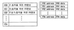
도 4는 세팅제어부(130) 내의 CS 버퍼의 구성 및 CS 버퍼에 기록된 하나의 CS(Command Set)의 구성을 나타내는 모식도이다. CS 버퍼에는 각 기능블럭의 FR 세팅을 위한 CS가 저장되며, 각 CS는 인덱스에 의해 구별된다. 세팅제어부(130)는 중앙처리부(110)로부터 실행모드로 설정된 세팅명령이 수신되면(즉, 모드 정보가 01 또는 10), 인덱스를 확인하여 특정 CS를 선택한다. 이 경우, 각 CS는 복수개의 FR 주소 및 이에 대응되는 FR 데이터로 구성되므로, 데이터 길이를 확인하여 실행할 CS의 길이를 선택한다. 이에 따라, 선택된 CS에 포함되는 FR 주소 및 FR 데이터를 해당 기능블럭에 전송하여 FR을 세팅하게 된다.4 is a schematic diagram showing the configuration of the CS buffer in the
도 3과 같은 세팅명령이 전송된 경우를 예를 들어 구체적으로 설명하면, 인덱스가 1이므로 CS1을 실행하게 된다. CS1은 제2기능블럭의 FR0 내지 FRm 주소, 및, FR0 내지 FRm 데이터로 구성된다. 한편, 데이터 길이가 4이므로, 제2기능블럭의 FR0 내지 FR3을 FR0 데이터 내지 FR3 데이터에 따라서 세팅하게 된다.For example, the case in which the setting command as shown in FIG. 3 is transmitted will be described in detail. Since the index is 1, CS1 is executed. CS1 is composed of FR0 to FRm addresses of the second functional block, and FR0 to FRm data. On the other hand, since the data length is 4, FR0 to FR3 of the second functional block are set according to the FR0 data to FR3 data.
한편, 도 3의 세팅 명령 중에서 모드 정보가 00인 경우를 가정하면, 로딩 모드이므로 지정된 메모리 주소(0x1000_0000)로부터 FR 주소 및 FR 데이터를 독출하여 지정된 CS에 기록하게 된다.On the other hand, assuming that the mode information is 00 in the setting command of FIG. 3, since it is a loading mode, the FR address and FR data are read from the designated memory address (0x1000_0000) and recorded in the designated CS.
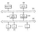
도 5는 본 발명의 제2실시예에 따른 제어시스템의 구성을 나타내는 모식도이다. 도 5에 따른 제어시스템은, 제1버스(210), 중앙처리부(220), 메모리(230), 세팅제어부(240), 제2버스(250), 버스인터페이스(bus interface : 260), 및, 복수개의 기능블럭(271, 272, ..., r)을 포함한다.5 is a schematic diagram showing the configuration of a control system according to a second embodiment of the present invention. The control system according to FIG. 5 includes a
제1버스(210)는 중앙처리부(220), 메모리(230), 세팅제어부(240) 간의 데이터 전송통로로써의 역할을 한다. 중앙처리부(220)는 제1버스(210)를 통해 세팅제어부(240)로 세팅명령을 전송하며, 세팅제어부(240)는 제1버스(210)를 통해 메모리(230)로부터 CS를 로딩하여 CS 버퍼에 저장하게 된다. 제1버스(210) 및 제2버스(250)는 버스인터페이스(260)를 통해 상호 연결된다.The
한편, 세팅제어부(240)는 별도의 제2버스(250)를 이용하여 각 기능블럭(271, 272, ..., r)의 FR을 세팅하게 된다. 즉, 세팅제어부(240)는 중앙처리부(220)로부터 특정 CS를 실행하라는 세팅명령이 입력되면, CS 버퍼에 기록된 FR 주소 및 FR 데이터를 제2버퍼(250)를 통해 해당 기능블럭에 전송하여 세팅한다. 본 실시예에 따르면, FR 세팅을 위한 제2버스(250)를 별도로 더 구비함으로써 버스 사용 효율을 높일 수 있다. 중앙처리부(220)에서 전송하는 세팅명령 및 CS 버퍼의 구조 등은 상술한 바와 같으므로 더이상의 설명은 생략한다.Meanwhile, the setting
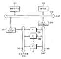
도 6은 본 발명의 제3실시예에 따른 제어 시스템의 구성을 나타내는 모식도이다. 도 6에 따른 제어시스템은, 제1버스(310), 중앙처리부(320), 메모리(330), 세팅제어부(340), 세팅컨트롤버스(350), 제2버스(360), 버스 인터페이스(370), 및, 복수개의 기능블럭(371, 372, ..., s)을 포함한다.6 is a schematic diagram showing the configuration of a control system according to a third embodiment of the present invention. The control system according to FIG. 6 includes a
중앙처리부(320)는 도 3에 도시된 바와 같은 구조의 세팅명령을 제1버스(310)를 통해 세팅제어부(340)로 전송한다. 이에 따라, 세팅제어부(340)는 지정된 CS를 로딩하거나, 세팅작업을 실행하게 된다. 이 경우, 세팅제어부(340)는 세팅컨트롤버스(350)를 이용하여 각 기능블럭(381, 382, ..., s)으로 FR데이터 등을 전송함으로써, FR을 세팅하게 된다. 세팅컨트롤버스(350)는 세팅작업을 위해 별도로 준비된 버스로써, 제1버스(310)를 효율적으로 이용하기 위한 것이다.The
한편, 각 기능블럭(371, 372, ..., s) 및 메모리(330) 간의 연결을 위해 별도로 제2버스(360) 및 버스 인터페이스(370)를 더 구비할 수도 있다. 이에 따라, 제1버스(310) 내에서의 전송지연 등을 방지할 수 있다. 세팅컨트롤버스(350)를 더 구비한다는 점을 제외하면, 도 6의 실시예도 상술한 실시예들과 동일한 방식으로 기능레지스터를 세팅하므로, 세팅방법에 대한 더 이상의 설명은 생략한다.Meanwhile, a
한편, 상술한 실시예 들에서 사용되는 버스는 일반적인 제어시스템에서 사용되는 AMBA AHB(Advanced Microcontroller Bus Architecture Advanced High- performance Bus), PCI(Peripheral Component Interconnect) 등이 될 수 있다.On the other hand, the bus used in the above-described embodiments may be an AMBA Advanced Microcontroller Bus Architecture Advanced High-performance Bus (AHB), Peripheral Component Interconnect (PCI), and the like used in a general control system.
도 7은 이러한 본 발명의 실시예에서 사용되는 세팅제어부(130, 240, 340)에서 각 기능블럭의 세팅을 제어하는 방법을 설명하기 위한 흐름도이다. 도 7에 따르면, 세팅제어부(130, 240, 340)는 중앙처리부(110, 220, 320)로부터 세팅명령이 수신되면(S710), 세팅명령 내의 모드정보를 확인하여 CS를 로딩할 것인지를 판단한다(S720).7 is a flowchart illustrating a method of controlling the setting of each functional block in the setting
이에 따라, CS를 로딩할 것으로 판단되면, 세팅명령 내에서 지정한 메모리주소로부터 CS를 독출한 후, 세팅명령 내에서 지정한 CS 인덱스에 따라 CS 버퍼내에 저장하는 로딩작업을 수행한다.Accordingly, when it is determined that the CS is to be loaded, the CS is read from the memory address specified in the setting command, and then the loading operation is performed in the CS buffer according to the CS index specified in the setting command.
한편, 세팅명령 내의 모드정보가 세팅을 실행하라는 실행모드인 것으로 판단되면(S740), 인덱스에 의해 지정된 CS를 각 기능블럭에 전송하여 FR을 세팅하게 된다. 이상과 같이, 세팅제어부(130, 240, 340)가 각 기능블럭의 FR 세팅작업을 전담하게 되므로, 중앙처리부(110, 220, 320)의 연산부담이 경감될 수 있다.On the other hand, if it is determined that the mode information in the setting command is the execution mode for executing the setting (S740), the CS designated by the index is transmitted to each function block to set the FR. As described above, since the setting
이러한 세팅방법은, 각 기능블럭 내에서 특정한 기능을 하기 위해 확보되는 특수기능레지스터(Special Function Register : SFR)에 특정 데이터를 세팅하는 경우에도 그대로 사용될 수 있다.This setting method can be used as it is even when setting specific data in a special function register (SFR) secured to perform a specific function in each function block.
이상 설명한 바와 같이, 본 발명에 따르면 제어시스템에 포함된 기능블럭 전부가 DMA 기능, 레지스터 자동세팅기능 등을 구비하지 않은 경우라도, 세팅제어부를 이용하여 각 기능블럭의 기능레지스터를 세팅하는 작업을 전담하도록 함으로써 중앙처리부를 효율적으로 사용할 수 있게 된다. 또한, 기능레지스터 세팅을 위한 버스를 추가로 구비함으로써 버스 사용효율도 높일 수 있다.As described above, according to the present invention, even if all of the function blocks included in the control system do not have the DMA function, the register automatic setting function, and the like, the task of setting the function registers of the respective function blocks by the setting control unit is dedicated. By doing so, the central processing unit can be used efficiently. In addition, the bus usage efficiency can be improved by additionally providing a bus for setting the functional register.
또한, 이상에서는 본 발명의 바람직한 실시예에 대하여 도시하고 설명하였지만, 본 발명은 상술한 특정의 실시예에 한정되지 아니하며, 청구범위에서 청구하는 본 발명의 요지를 벗어남이 없이 당해 발명이 속하는 기술분야에서 통상의 지식을 가진자에 의해 다양한 변형실시가 가능한 것은 물론이고, 이러한 변형실시들은 본 발명의 기술적 사상이나 전망으로부터 개별적으로 이해되어져서는 안될 것이다.In addition, although the preferred embodiment of the present invention has been shown and described above, the present invention is not limited to the specific embodiments described above, but the technical field to which the invention belongs without departing from the spirit of the invention claimed in the claims. Of course, various modifications can be made by those skilled in the art, and these modifications should not be individually understood from the technical spirit or the prospect of the present invention.
Claims (9)
Translated fromKoreanPriority Applications (2)
| Application Number | Priority Date | Filing Date | Title |
|---|---|---|---|
| KR1020040064308AKR100615694B1 (en) | 2004-08-16 | 2004-08-16 | Control system to control multiple function blocks |
| US11/201,114US20060036779A1 (en) | 2004-08-16 | 2005-08-11 | Method and control system for controlling a plurality of function blocks |
Applications Claiming Priority (1)
| Application Number | Priority Date | Filing Date | Title |
|---|---|---|---|
| KR1020040064308AKR100615694B1 (en) | 2004-08-16 | 2004-08-16 | Control system to control multiple function blocks |
Publications (2)
| Publication Number | Publication Date |
|---|---|
| KR20060015917A KR20060015917A (en) | 2006-02-21 |
| KR100615694B1true KR100615694B1 (en) | 2006-08-25 |
Family
ID=35801328
Family Applications (1)
| Application Number | Title | Priority Date | Filing Date |
|---|---|---|---|
| KR1020040064308AExpired - Fee RelatedKR100615694B1 (en) | 2004-08-16 | 2004-08-16 | Control system to control multiple function blocks |
Country Status (2)
| Country | Link |
|---|---|
| US (1) | US20060036779A1 (en) |
| KR (1) | KR100615694B1 (en) |
Families Citing this family (5)
| Publication number | Priority date | Publication date | Assignee | Title |
|---|---|---|---|---|
| KR20150010135A (en)* | 2013-07-18 | 2015-01-28 | 에스케이하이닉스 주식회사 | Semiconductor device and memory system having the same |
| US10210350B2 (en) | 2015-08-10 | 2019-02-19 | Samsung Electronics Co., Ltd. | Electronic device against side channel attacks |
| DE102020106357A1 (en) | 2019-03-11 | 2020-09-17 | Samsung Electronics Co., Ltd. | STORAGE DEVICE AND INSTRUCTION RING STORAGE QUEUE PROCEDURE |
| CN111679785B (en) | 2019-03-11 | 2025-03-11 | 三星电子株式会社 | Memory device for processing operation and operation method thereof, and data processing system |
| DE102020105628A1 (en) | 2019-03-11 | 2020-09-17 | Samsung Electronics Co., Ltd. | Method for performing internal processing operations with a predefined protocol interface of a storage device |
Family Cites Families (4)
| Publication number | Priority date | Publication date | Assignee | Title |
|---|---|---|---|---|
| JP2002342259A (en)* | 2001-05-21 | 2002-11-29 | Hitachi Ltd | DMA controller and automatic DMA controller generation device |
| KR100462177B1 (en)* | 2002-08-26 | 2004-12-17 | 삼성전자주식회사 | Embedded controller capable of backing up operating states of a peripheral device in the real time |
| KR100487539B1 (en)* | 2002-09-02 | 2005-05-03 | 삼성전자주식회사 | Nonvolatile semiconductor memory device for connecting to serial advanced techonology attachement cable |
| JP4241625B2 (en)* | 2003-03-31 | 2009-03-18 | 富士通マイクロエレクトロニクス株式会社 | Semiconductor device |
- 2004
- 2004-08-16KRKR1020040064308Apatent/KR100615694B1/ennot_activeExpired - Fee Related
- 2005
- 2005-08-11USUS11/201,114patent/US20060036779A1/ennot_activeAbandoned
Also Published As
| Publication number | Publication date |
|---|---|
| US20060036779A1 (en) | 2006-02-16 |
| KR20060015917A (en) | 2006-02-21 |
Similar Documents
| Publication | Publication Date | Title |
|---|---|---|
| US6954806B2 (en) | Data transfer apparatus and method | |
| CN112631969B (en) | Virtual multichannel data transmission method and system based on PCIE interface | |
| US8266371B2 (en) | Non-volatile storage device, host device, non-volatile storage system, data recording method, and program | |
| JPH11250228A (en) | Image processing apparatus and image processing system | |
| CN102918515B (en) | Store data in the multiple impact dampers in Memory Controller any in | |
| CN111782154A (en) | Data moving method, device and system | |
| CN112445412A (en) | Data storage method and device | |
| KR101459200B1 (en) | Transmission control device, memory control device, and plc provided with the transmission control device | |
| KR100615694B1 (en) | Control system to control multiple function blocks | |
| US20080109627A1 (en) | Nonvolatile Memory Device And Method For Accessing Nonvolatile Memory Device | |
| CN112764673B (en) | Hyperspectral linear array data storage rate optimization method, device and storage medium | |
| CN106980513A (en) | A kind of switching method and device of dual boot file | |
| CN117008843B (en) | Control page linked list construction device and electronic equipment | |
| JPH0776932B2 (en) | Data transmission method | |
| CN118363662A (en) | Configuration method, device and storage system of memory register | |
| JPH11232213A (en) | Data transfer system for input/output device | |
| KR100950356B1 (en) | Data transmission unit supporting multiple coherency units | |
| CN113032300A (en) | Data transmission control method | |
| CN117811939B (en) | Remote terminal simulation method based on 1553B bus | |
| CN106294207B (en) | Data feedback method, buffer, controller and system | |
| CN100371916C (en) | SCSI magnetic disc recording device and mehtod | |
| CN113032301B (en) | Memory controller, system on chip and electronic device | |
| JP4723334B2 (en) | DMA transfer system | |
| CN111045961A (en) | Data processing method and storage controller using the same | |
| JPH04277850A (en) | Descriptor control system |
Legal Events
| Date | Code | Title | Description |
|---|---|---|---|
| A201 | Request for examination | ||
| PA0109 | Patent application | St.27 status event code:A-0-1-A10-A12-nap-PA0109 | |
| PA0201 | Request for examination | St.27 status event code:A-1-2-D10-D11-exm-PA0201 | |
| PN2301 | Change of applicant | St.27 status event code:A-3-3-R10-R13-asn-PN2301 St.27 status event code:A-3-3-R10-R11-asn-PN2301 | |
| PN2301 | Change of applicant | St.27 status event code:A-3-3-R10-R13-asn-PN2301 St.27 status event code:A-3-3-R10-R11-asn-PN2301 | |
| E902 | Notification of reason for refusal | ||
| PE0902 | Notice of grounds for rejection | St.27 status event code:A-1-2-D10-D21-exm-PE0902 | |
| PG1501 | Laying open of application | St.27 status event code:A-1-1-Q10-Q12-nap-PG1501 | |
| P11-X000 | Amendment of application requested | St.27 status event code:A-2-2-P10-P11-nap-X000 | |
| P13-X000 | Application amended | St.27 status event code:A-2-2-P10-P13-nap-X000 | |
| E701 | Decision to grant or registration of patent right | ||
| PE0701 | Decision of registration | St.27 status event code:A-1-2-D10-D22-exm-PE0701 | |
| GRNT | Written decision to grant | ||
| PR0701 | Registration of establishment | St.27 status event code:A-2-4-F10-F11-exm-PR0701 | |
| PR1002 | Payment of registration fee | St.27 status event code:A-2-2-U10-U11-oth-PR1002 Fee payment year number:1 | |
| PG1601 | Publication of registration | St.27 status event code:A-4-4-Q10-Q13-nap-PG1601 | |
| LAPS | Lapse due to unpaid annual fee | ||
| PC1903 | Unpaid annual fee | St.27 status event code:A-4-4-U10-U13-oth-PC1903 Not in force date:20090818 Payment event data comment text:Termination Category : DEFAULT_OF_REGISTRATION_FEE | |
| PC1903 | Unpaid annual fee | St.27 status event code:N-4-6-H10-H13-oth-PC1903 Ip right cessation event data comment text:Termination Category : DEFAULT_OF_REGISTRATION_FEE Not in force date:20090818 | |
| R18-X000 | Changes to party contact information recorded | St.27 status event code:A-5-5-R10-R18-oth-X000 |