KR100614652B1 - Image processing apparatus and method with reduced power consumption - Google Patents
Image processing apparatus and method with reduced power consumptionDownload PDFInfo
- Publication number
- KR100614652B1 KR100614652B1KR20040091505AKR20040091505AKR100614652B1KR 100614652 B1KR100614652 B1KR 100614652B1KR 20040091505 AKR20040091505 AKR 20040091505AKR 20040091505 AKR20040091505 AKR 20040091505AKR 100614652 B1KR100614652 B1KR 100614652B1
- Authority
- KR
- South Korea
- Prior art keywords
- image data
- data
- line memory
- pixel
- data segment
- Prior art date
- Legal status (The legal status is an assumption and is not a legal conclusion. Google has not performed a legal analysis and makes no representation as to the accuracy of the status listed.)
- Expired - Fee Related
Links
Images


Classifications
- H—ELECTRICITY
- H04—ELECTRIC COMMUNICATION TECHNIQUE
- H04N—PICTORIAL COMMUNICATION, e.g. TELEVISION
- H04N1/00—Scanning, transmission or reproduction of documents or the like, e.g. facsimile transmission; Details thereof
- H04N1/41—Bandwidth or redundancy reduction
- H—ELECTRICITY
- H04—ELECTRIC COMMUNICATION TECHNIQUE
- H04N—PICTORIAL COMMUNICATION, e.g. TELEVISION
- H04N19/00—Methods or arrangements for coding, decoding, compressing or decompressing digital video signals
- H04N19/42—Methods or arrangements for coding, decoding, compressing or decompressing digital video signals characterised by implementation details or hardware specially adapted for video compression or decompression, e.g. dedicated software implementation
- H04N19/423—Methods or arrangements for coding, decoding, compressing or decompressing digital video signals characterised by implementation details or hardware specially adapted for video compression or decompression, e.g. dedicated software implementation characterised by memory arrangements
Landscapes
- Engineering & Computer Science (AREA)
- Multimedia (AREA)
- Signal Processing (AREA)
- Compression Or Coding Systems Of Tv Signals (AREA)
- Studio Devices (AREA)
- Compression Of Band Width Or Redundancy In Fax (AREA)
- Editing Of Facsimile Originals (AREA)
Abstract
Translated fromKoreanDescription
Translated fromKorean도 1은 통상적인 VGA(Variable Graphics Array) 표준의 화상 처리 장치를 개략적으로 도시한 블록도;1 is a block diagram schematically showing an image processing apparatus of a conventional Variable Graphics Array (VGA) standard;
도 2는 카메라 프로세서로부터의 화상 데이터가 라스터 스캔 순서로 라인 메모리에 기입되는 것을 보여주는 도면;2 shows that image data from a camera processor is written to the line memory in raster scan order;
도 3은 라인 메모리에 저장된 화상 데이터가 블록 스캔 순서로 독출되는 것을 보여주는 도면;3 is a diagram showing that image data stored in a line memory is read out in block scan order;
도 4는 본 발명의 바람직한 실시예에 따른 화상 데이터 처리 장치를 보여주는 블록도;4 is a block diagram showing an image data processing apparatus according to a preferred embodiment of the present invention;
도 5는 VGA 표준에 따른 한 프레임의 영상 데이터를 보여주는 도면;5 shows image data of one frame according to the VGA standard;
도 6은 도 5에 도시된 한 페이즈를 구체적으로 보여주는 도면;FIG. 6 shows a phase specifically shown in FIG. 5; FIG.
도 7은 도 4에 도시된 라인 메모리(130)의 바람직한 실시예를 보여주는 도면;FIG. 7 shows a preferred embodiment of the
도 8은 카메라 프로세서(110)로부터 출력되는 화상 데이터를 보여주는 도면;8 shows image data output from the
도 9a 내지 도 9d는 조합기(120)로부터 출력되는 한 페이즈의 데이터 세그먼트들이 라인 메모리(130)에 기입된 예들을 보여주는 도면들;9A-9D show examples in which one phase of data segments output from combiner 120 is written into
도 10a 및 도 10b는 데이터 세그먼트들이 라인 메모리(130)로부터/에 독출/기입될 때 신호들의 타이밍도들; 그리고10A and 10B are timing diagrams of signals as data segments are read / written from / from
도 11은 해상도가 VGA인 경우 컬러 성분 데이터를 라인 메모리에 저장할 때 0.13um에서의 전력 소비량을 보여주고 있다.FIG. 11 shows power consumption at 0.13 um when color component data is stored in the line memory when the resolution is VGA.
*도면의 주요 부분에 대한 설명* Description of the main parts of the drawing
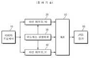
100 : 화상 데이터 처리 장치110 : 카메라 프로세서100: image data processing device 110: camera processor
120 : 조합기130 : 라인 메모리120: combiner 130: line memory
140 : 어드레스 발생기150 : 분리기140: address generator 150: separator
160 : JPEG 엔진160: JPEG engine
본 발명은 화상 처리 장치 및 방법에 관한 것으로, 좀 더 구체적으로는 하나의 라인 메모리를 사용하여 라스터 스캔 순서의 화상 데이터와 블록 스캔 순서의 화상 데이터 사이의 상호 변환을 처리하는 화상 처리 장치 및 방법에 관한 것이다.The present invention relates to an image processing apparatus and method, and more particularly, to an image processing apparatus and method for processing mutual conversion between raster scan order image data and block scan order image data using one line memory. It is about.
잘 알려진 바와 같이, JPEG(Joint Photographic Experts Group)은 데이터 압축을 위해 이산 코사인 변환(Discrete Cosine Transform:DCT)을 사용한다. DCT 압축 기술은 데이터를 8픽셀*8픽셀 단위의 블록으로 나누어 데이터를 처리한다. 하지만 카메라의 화상 처리부는 화상 데이터를 라인 단위로, 즉, 라스터 포맷(raster format)(라스터 스캔 순서:한 화상 전체에 대해서 좌에서 우로, 위에서 아래로)으 로 연속적으로 출력한다. 따라서, 라스터 스캔 순서의 화상 데이터를 블록 스캔 순서로 변환하기 위해서는, 최소 8 라인의 화상 데이터를 저장할 수 있는 라인 메모리가 필요하다. 8 라인이 저장된 라인 메모리로부터 8*8 픽셀의 화상 블록을 만드는 동안 카메라의 화상 처리부는 새로운 화상 데이터를 출력하기 때문에 연속적인 처리를 위해서는 8 라인의 라인 메모리가 더 필요하다. 즉, 하나의 라인 메모리에 화상 데이터가 기입되는 동안 다른 라인 메모리에 저장된 화상 데이터에 대한 8*8 블록 독출이 이루어진다. 화상 데이터는 휘도 성분 Y와 색차 성분 U 및 V로 구성되기 때문에 이들 각각의 성분들에 대해서 두 개의 라인 메모리가 필요하다.As is well known, the Joint Photographic Experts Group (JPEG) uses Discrete Cosine Transform (DCT) for data compression. DCT compression technology processes data by dividing it into blocks of 8 pixels by 8 pixels. However, the image processing unit of the camera continuously outputs the image data in line units, that is, in raster format (raster scan order: from left to right and top to bottom for an entire image). Therefore, in order to convert the image data in the raster scan order into the block scan order, a line memory capable of storing at least eight lines of image data is required. Since the image processing section of the camera outputs new image data while making an image block of 8 * 8 pixels from the line memory in which eight lines are stored, eight more line memories are required for continuous processing. That is, while the image data is written in one line memory, 8 * 8 block reads are performed on the image data stored in the other line memory. Since the image data is composed of the luminance component Y and the chrominance components U and V, two line memories are required for each of these components.
도 1은 통상적인 VGA(Variable Graphics Array) 표준의 화상 처리 장치를 개략적으로 도시한 블록도로서, 단지 휘도 성분 Y에 대한 라인 메모리 시스템을 도시한다. 카메라 프로세서(10)에서 첫 번째 8 라인의 휘도 Y 성분이 출력되어 라인 메모리_Y0(20)에 순차적으로 저장된다. 두 번째 8 라인의 휘도 성분 Y가 라인 메모리_Y1(40)에 순차적으로 저장됨과 동시에 라인 메모리_Y0(20)에 대한 8*8 블록 단위 독출이 이루어진다. 이 때, 멀티플렉서(50)는 어드레스 발생 회로(30)의 제어에 응답해서 라인 메모리_Y0(12)로부터 독출된 8*8 화상 블록을 JPEG 엔진(22)으로 전달한다. 라인 메모리들(20, 40)에 대한 기입 및 독출 어드레스는 어드레스 발생 회로(30)에서 생성된다.Fig. 1 is a block diagram schematically showing an image processing apparatus of a conventional Variable Graphics Array (VGA) standard, showing only a line memory system for luminance component Y. The luminance Y component of the first eight lines is output from the
도 2는 카메라 프로세서(10)로부터의 화상 데이터가 라스터 스캔 순서로 라인 메모리에 기입되는 것을 보여주고 있고, 도 3은 라인 메모리에 저장된 화상 데이터가 블록 스캔 순서로 독출되는 것을 보여주고 있다. 도 2 및 도 3에서, 수평 방향 픽셀 수는 640이고, V는 수직 방향 픽셀 수(즉, 라인 수)는 480이다. 하나의 라인 메모리에는 8 개의 라인들에 속하는 640*8 픽셀들의 데이터가 저장된다. 하나의 픽셀의 데이터가 8-bit이면, 라인 메모리의 크기(size)는 640*8*8 비트이다. 이 실시예에서는, VGA를 기준으로 설명하나, 해상도에 따라서 라인 메모리의 크기는 변경된다.2 shows that the image data from the
다시 도 1을 참조하면, 라인 메모리들(20, 40)에 대한 기입 어드레스는 0 부터 640*8-1까지 순차적으로 증가한다.Referring back to FIG. 1, the write addresses for the
블록 단위 독출을 위한 라인 메모리들에 대한 독출 어드레스(raddr)는 아래 수학식 1에 기재된 알고리즘에 따라 정해진다. 또한, 시스템 클럭 신호에 동기해서 하나의 픽셀 데이터가 카메라 프로세서(10)로부터 출력될 때마다 기입 어드레스(waddr)이 순차적으로 증가한다. M[0][] 및 M[1][]은 8-bit 단위로 액세스가 가능한 라인 메모리들(20, 40)을 가리킨다.The read address raddr for the line memories for block unit read is determined according to the algorithm described in
parity = 0;parity = 0;
for(i=0; i<640; i++){for (i = 0; i <640; i ++) {
waddr = 0;waddr = 0;
for(v=0; v<8; v++){for (v = 0; v <8; v ++) {
for(h=0; h<8; h++){for (h = 0; h <8; h ++) {
raddr=v * 640 + i * 8 + h;raddr = v * 640 + i * 8 + h;
dout = M[parity][raddr];dout = M [parity] [raddr];
M[~parity][waddr] = din;M [~ parity] [waddr] = din;
waddr++;waddr ++;
}}
}}
parity = ~parity;parity = ~ parity;
}}
독출 어드레스(raddr)는 아래 수학식 2에 기재된 알고리즘에 따라서 구해질 수도 있다.The read address raddr may be obtained according to the algorithm described in
parity = 0;parity = 0;
for(i=0; i<imax ;i++){for (i = 0; i <imax; i ++) {
waddr = 0;waddr = 0;
for(v=0; v<8; v++){for (v = 0; v <8; v ++) {
addrp = (v*80 + i)<<3;addrp = (v * 80 + i) << 3;
for(h=0; h<8; h++){for (h = 0; h <8; h ++) {
raddr=addrp + h;raddr = addrp + h;
dout = M[parity][raddr];dout = M [parity] [raddr];
M[~parity][waddr] = din;M [~ parity] [waddr] = din;
waddr++;waddr ++;
}}
}}
parity = ~parity;parity = ~ parity;
}}
여기서, i는 블록 순서를, v는 한 블록에서 수직 방향 라인 순서를, 그리고 h는 하나의 블록에 포함되는 수평 방향 픽셀의 순서를 나타낸다.Here, i denotes a block order, v denotes a vertical line order in one block, and h denotes an order of horizontal pixels included in one block.
이와 같은 통상적인 화상 처리 방법은 각 색 성분에 대하여 두 개의 라인 메모리들을 사용한다. 예컨대, VGA 표준의 경우, 휘도 성분 Y에 대해서 640*8바이트의 라인 메모리를 두 개 사용한다. 따라서, 시스템의 저전력화를 위해 메모리를 칩에 내장할 경우, 칩 크기가 증가하는 문제점이 발생한다. 특히 처리하고자 하는 화상의 크기가 증가할수록 그 문제는 더욱 심각해진다.This conventional image processing method uses two line memories for each color component. For example, in the VGA standard, two line memories of 640 * 8 bytes are used for the luminance component Y. Therefore, when the memory is embedded in the chip for lowering the system, a problem arises in that the chip size increases. In particular, as the size of the image to be processed increases, the problem becomes more serious.
본 출원인에 의해 "라스터 스캔 순서 화상 데이터와 블록 스캔 순서 화상 데이터 사이의 변환을 위한 화상 처리 장치 및 방법"이란 제목으로 2002년 11월 7일 출원된 국내공개특허공보 2004-40677호는 이와 같은 문제점을 해결하기 위해 제안되었다.Korean Patent Application Publication No. 2004-40677 filed November 7, 2002 entitled "Image Processing Apparatus and Method for Conversion Between Raster Scan Sequence Image Data and Block Scan Sequence Image Data" by the applicant, It was proposed to solve the problem.
상기 특허는, 각 색 성분에 대하여 하나의 라인 메모리들을 사용함으로써 화상 처리 장치의 크기를 감소시켰다. 그러나, 상기 특허는 매 픽셀 데이터마다 라인 메모리를 액세스하여 기입/독출 동작이 수행되도록 함으로써 전력 소비가 크다는 단점이 있다.The patent reduces the size of the image processing apparatus by using one line memories for each color component. However, the patent has a disadvantage in that power consumption is high by accessing the line memory every pixel data so that a write / read operation is performed.
따라서 본 발명의 목적은 라인 메모리의 크기를 감소시킬 수 있는 라스터 스캔 순서와 블록 스캔 순서 사이의 화상 데이터를 상호 변환하되, 전력 소비가 감소된 화상 처리 장치를 제공하는데 있다.Accordingly, an object of the present invention is to provide an image processing apparatus which converts image data between a raster scan order and a block scan order which can reduce the size of the line memory, but reduces power consumption.
본 발명의 다른 목적은 하나의 라인 메모리를 사용하여 라스터 스캔 순서와 블록 스캔 순서 사이의 화상 데이터를 상호 변환하되, 전력 소비가 감소된 어드레스 발생기를 제공하는데 있다.Another object of the present invention is to provide an address generator which converts image data between a raster scan order and a block scan order using one line memory, but reduces power consumption.
본 발명의 또 다른 목적은 라인 메모리의 크기를 감소시킬 수 있는 라스터 스캔 순서와 블록 스캔 순서 사이의 화상 데이터를 상호 변환하되, 전력 소비가 감소된 화상 처리 방법을 제공하는데 있다.It is still another object of the present invention to provide an image processing method in which power consumption is reduced while converting image data between a raster scan order and a block scan order that can reduce the size of the line memory.
상술한 바와 같은 목적을 달성하기 위한 본 발명의 화상 데이터 처리 장치는: 라스터 스캔 순서의 화상 데이터를 픽셀 단위로 공급하는 화상 데이터 처리기와, 상기 화상 데이터 처리기로부터 n 개의 픽셀들의 화상 데이터를 순차적으로 입력받아서 하나의 데이터 세그먼트로 조합하는 조합기와, 기입 인에이블 신호, 독출 인에이블 신호 및 어드레스 신호를 발생하는 어드레스 발생기와, 상기 어드레스 신호 및 상기 기입 인에이블 신호에 응답해서 상기 조합기로부터의 데이터 세그먼트를 저장하고, 그리고 상기 어드레스 신호 및 상기 독출 인에이블 신호에 응답해서 저장된 데이터 세그먼트를 출력하는 라인 메모리와, 상기 라인 메모리로부터 출력된 데이터 세그먼트를 n 개의 픽셀들의 화상 데이터로 분리하는 분리기, 그리고 상 기 분리기로부터 각 픽셀의 화상 데이터를 순차적으로 입력받는 영상 처리 엔진을 포함한다.An image data processing apparatus of the present invention for achieving the above object includes: an image data processor for supplying image data in a raster scan order on a pixel basis, and image data of n pixels sequentially from the image data processor; A combiner that receives the input and combines it into one data segment, an address generator that generates a write enable signal, a read enable signal and an address signal, and a data segment from the combiner in response to the address signal and the write enable signal. A line memory for storing and outputting a stored data segment in response to the address signal and the read enable signal, a separator for separating the data segment output from the line memory into n pixels of image data, and the separator. From each And an image processing engine that sequentially receives pixel image data.
바람직한 실시예에 있어서, 상기 어드레스 발생기는, 상기 라인 메모리에 저장된 상기 데이터 세그먼트들이 블록 스캔 순서로 독출되도록 상기 어드레스 신호를 발생한다.In a preferred embodiment, the address generator generates the address signal such that the data segments stored in the line memory are read in block scan order.
바람직한 실시예에 있어서, 상기 조합기는, 클럭 신호에 동기해서 상기 화상 데이터 처리기로부터 n 개의 픽셀들의 화상 데이터를 순차적으로 입력받는다.In a preferred embodiment, the combiner sequentially receives n pixel image data from the image data processor in synchronization with a clock signal.
이 실시예에 있어서, 상기 분리기는, 상기 클럭 신호에 동기해서 상기 라인 메모리로부터 출력된 데이터 세그먼트를 n 개의 픽셀들의 화상 데이터로 분리한다.In this embodiment, the separator separates the data segment output from the line memory into n pixel data in synchronization with the clock signal.
이 실시예에 있어서, 상기 기입 인에이블 신호는 상기 조합기로부터 상기 데이터 세그먼트가 출력되고 나서 다음 데이터 세그먼트가 출력되기 전에 활성화된다.In this embodiment, the write enable signal is activated after the data segment is output from the combiner but before the next data segment is output.
이 실시예에 있어서, 상기 독출 인에이블 신호는 상기 기입 인에이블 신호보다 먼저 활성화된다.In this embodiment, the read enable signal is activated before the write enable signal.
이 실시예에 있어서, 상기 영상 처리 엔진은 JPEG(Joint Photographic Expert Group) 엔진이고, 상기 JPEG 엔진은 8 픽셀*8 픽셀 단위 블록의 영상 데이터를 처리한다.In this embodiment, the image processing engine is a Joint Photographic Expert Group (JPEG) engine, and the JPEG engine processes image data of 8 pixel * 8 pixel unit blocks.
이 실시예에 있어서, 상기 화상 데이터 처리기는, 수평 해상도(H) 및 수직 해상도(V)에 따른 H*V 픽셀 화상 데이터를 순차적으로 출력하며, 상기 H*V 픽셀 화상 데이터는, 각각이 상기 수평 해상도(H)*8 픽셀들을 포함하는 (V/8) 개의 페이즈 들로 나뉘어진다.In this embodiment, the image data processor sequentially outputs H * V pixel image data according to horizontal resolution (H) and vertical resolution (V), wherein the H * V pixel image data is each horizontal Resolution (H) is divided into (V / 8) phases containing 8 pixels.
이 실시예에 있어서, 상기 라인 메모리로부터 출력되는 상기 데이터 세그먼트는 이전 페이즈의 데이터 세그먼트이다.In this embodiment, the data segment output from the line memory is the data segment of the previous phase.
이 실시예에 있어서, 상기 라인 메모리에 저장되는 상기 데이터 세그먼트는 현재 페이즈의 데이터 세그먼트이다.In this embodiment, the data segment stored in the line memory is the data segment of the current phase.
이 실시예에 있어서, 상기 라인 메모리는, (상기 수평 해상도(H) * 8 * 각 픽셀의 데이터 비트 수)의 크기이다.In this embodiment, the line memory is the size of (the horizontal resolution (H) * 8 * the number of data bits of each pixel).
이 실시예에 있어서, 상기 조합기는, 상기 화상 데이터 처리기로부터 8 개의 픽셀들의 화상 데이터를 순차적으로 입력받아서 하나의 데이터 세그먼트로 조합하며, 상기 데이터 세그먼트의 크기는 (8 픽셀 * 한 픽셀의 데이터 크기)이다.In this embodiment, the combiner sequentially receives the image data of eight pixels from the image data processor and combines them into one data segment, and the size of the data segment is (8 pixels * data size of one pixel). to be.
본 발명의 다른 특징에 따른 라스터 스캔 순서의 화상 데이터를 블록 스캔 순서의 화상 데이터로 변환하기 위한 화상 데이터 처리 방법은: 상기 라스터 스캔 순서의 화상 데이터를 순차적으로 공급받는 단계와, n 개의 픽셀에 대한 화상 데이터를 하나의 데이터 세그먼트로 조합하는 단계와, 어드레스 신호를 발생하는 단계와, 상기 어드레스 신호 및 독출 인에이블 신호에 응답해서 라인 메모리에 저장된 이전 페이즈의 데이터 세그먼트를 독출하는 단계와, 상기 어드레스 신호 및 기입 인에이블 신호에 응답해서 현재 페이즈의 상기 데이터 세그먼트를 상기 라인 메모리에 저장하는 단계와, 상기 독출된 데이터 세그먼트를 n 개의 픽셀들의 화상 데이터로 분리하는 단계, 그리고 상기 분리된 n 개의 픽셀들의 화상 데이터를 순차적으로 영상 처리 엔진으로 제공하는 단계를 포함한다.According to another aspect of the present invention, an image data processing method for converting image data in raster scan order into image data in block scan order includes: sequentially receiving image data in raster scan order and n pixels; Combining the image data for the data into one data segment, generating an address signal, reading a data segment of a previous phase stored in a line memory in response to the address signal and the read enable signal; Storing the data segment of the current phase in the line memory in response to the address signal and write enable signal, separating the read data segment into image data of n pixels, and the separated n Image data of the pixels are sequentially transferred to the image processing engine. Providing a step.
바람직한 실시예에 있어서, 상기 독출 인에이블 신호는 상기 기입 인에이블 신호보다 먼저 활성화된다.In a preferred embodiment, the read enable signal is activated before the write enable signal.
바람직한 실시예에 있어서, 상기 어드레스 신호 발생 단계는, 상기 라인 메모리에 저장된 상기 데이터 세그먼트들이 블록 스캔 순서로 독출되도록 상기 어드레스 신호를 발생한다.In the preferred embodiment, the address signal generating step generates the address signal such that the data segments stored in the line memory are read in a block scan order.
이 실시예에 있어서, 상기 영상 처리 엔진은 JPEG(Joint Photographic Expert Group) 엔진이고, 상기 JPEG 엔진은 8 픽셀*8 픽셀 단위 블록의 영상 데이터를 처리한다.In this embodiment, the image processing engine is a Joint Photographic Expert Group (JPEG) engine, and the JPEG engine processes image data of 8 pixel * 8 pixel unit blocks.
이 실시예에 있어서, 상기 라스터 스캔 순서의 화상 데이터를 순차적으로 공급받는 단계는, 수평 해상도(H) 및 수직 해상도(V)에 따른 H*V 픽셀 화상 데이터를 순차적으로 공급하며, 상기 H*V 픽셀 화상 데이터는, 각각이 상기 수평 해상도(H)*8 픽셀들을 포함하는 (V/8) 개의 페이즈들로 나뉘어진다.In this embodiment, the step of sequentially receiving the image data in the raster scan order, sequentially supply H * V pixel image data according to the horizontal resolution (H) and vertical resolution (V), the H * The V pixel image data is divided into (V / 8) phases, each containing the horizontal resolution H * 8 pixels.
이 실시예의 상기 독출 단계에서, 상기 라인 메모리로부터 독출되는 상기 데이터 세그먼트는 이전 페이즈의 데이터 세그먼트이다.In the read step of this embodiment, the data segment read from the line memory is the data segment of the previous phase.
이 실시예의 상기 저장 단계에서, 상기 라인 메모리에 저장되는 상기 데이터 세그먼트는 현재 페이즈의 데이터 세그먼트이다.In the storing step of this embodiment, the data segment stored in the line memory is a data segment of the current phase.
이 실시예에 있어서, 상기 라인 메모리의 크기는, (상기 수평 해상도(H) * 8 * 각 픽셀의 데이터 비트 수)이다.In this embodiment, the size of the line memory is (the horizontal resolution (H) * 8 * the number of data bits of each pixel).
이 실시예에 있어서, 상기 데이터 세그먼트의 크기는 (8 픽셀 * 한 픽셀의 데이터 크기)이다.In this embodiment, the size of the data segment is (8 pixels * data size of one pixel).
상술한 바와 같은 화상 처리 장치 및 방법은, 특히, 라스터 포맷을 블록 포맷으로 전환할 때, 카메라 프로세서에서 발생된 화상 데이터를 각 색 성분별로 분리하여 하나의 라인 메모리에 저장한 후, 블록 포맷으로 읽기에 적합한 순서로 블록 단위로 독출하여 JPEG 엔진으로 전달한다. 하나의 통합 라인 메모리를 사용하기 때문에 메모리 크기를 줄일 수 있고 이에 따라 칩 사이즈를 감소시킬 수 있다. 특히, 하나의 블록에 포함된 라인 단위로 라인 메모리를 액세스함으로써 전력 소비가 감소된다.The image processing apparatus and method as described above, in particular, when converting a raster format into a block format, separates the image data generated by the camera processor for each color component, stores them in one line memory, and then converts the image data into a block format. It reads block by block in the proper order and delivers it to JPEG engine. By using one integrated line memory, the memory size can be reduced, thereby reducing the chip size. In particular, power consumption is reduced by accessing the line memory in units of lines included in one block.
(실시예)(Example)
이하 본 발명의 바람직한 실시예를 첨부된 도면들을 참조하여 상세히 설명한다. 도 4는 본 발명의 바람직한 실시예에 따른 화상 데이터 처리 장치를 보여주는 블록도이다. 도 4를 참조하면, 본 발명의 화상 데이터 처리 장치(100)는 카메라 프로세서(110), 조합기(packer, 120), 라인 메모리(130), 어드레스 발생기(140), 분리기(unpacker, 150) 및 JPEG 엔진(160)을 포함한다.Hereinafter, exemplary embodiments of the present invention will be described in detail with reference to the accompanying drawings. 4 is a block diagram showing an image data processing apparatus according to a preferred embodiment of the present invention. Referring to FIG. 4, the image
카메라 프로세서(110)는 라스터 스캔 순서로 화상 데이터를 출력한다. 화상 데이터는 휘도 성분 Y와 색차 성분 U, V를 포함하며, 도면에는 단지 휘도 성분 Y를 위한 라인 메모리Y(130)를 도시하였다. 카메라 프로세서(110)는 클럭 신호에 동기화하여 화상 데이터를 출력하며, 출력된 휘도 성분 Y는 라인 메모리(130)에 저장된다. 처리하고자 하는 화상 데이터의 해상도가 H*V이고, JPEG 엔진(160)이 h*v 블록 단위로 화상 데이터를 처리한다면, 라인 메모리_Y(130)는 H*v 바이트의 크기를 갖는다. 예컨대, 카메라 프로세서(110)의 해상도가 VGA 표준인 640*480이고, JPEG 압축 방식의 경우, H=640, V=480 그리고 h=v=8이다. 이하에서는 VGA 표준에서 h와 v가 8인 경우를 예로 들어 설명한다.The
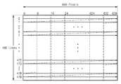
도 5는 VGA 표준에 따른 한 프레임의 영상 데이터를 보여주고 있다. 한 프레임은 가로로 640 픽셀, 세로로 480 픽셀 즉, 640*480=307,200 픽셀을 포함한다. 도 4에 도시된 라인 메모리(130)는 640*8 픽셀의 화상 데이터를 저장할 수 있는 크기를 갖는다. 한 프레임은 480/8 즉, 60개의 페이즈들(Phase1-Phase60)을 포함한다. 즉, 한 페이즈의 화상 데이터가 라인 메모리(130)에 동시에 저장될 수 있다.5 shows image data of one frame according to the VGA standard. One frame contains 640 pixels horizontally and 480 pixels vertically, that is, 640 * 480 = 307,200 pixels. The
앞서 설명한 바와 같이, JPEG 엔진(160)의 DCT 압축 기술은 8픽셀*8픽셀 크기의 블록 단위로 화상 데이터를 처리한다. 한 프레임은 80 개의 블록들(B0-B79)로 나뉘어진다.As described above, the DCT compression technique of the
도 6은 도 5에 도시된 한 페이즈를 구체적으로 보여주는 도면이다. 하나의 블록은 가로로 8 개의 픽셀들과 세로로 8 개의 픽셀들 즉, 8 개의 라인들(L0-L7)을 포함한다. 이하 설명에서, 한 블록 내 특정 라인에 속하는 8 개의 픽셀들은 '데이터 세그먼트'라 지칭한다. 그러므로, 하나의 블록은 8 개의 세그먼트들을 포함하며, 한 페이즈는 640 개의 세그먼트들(S0-S639)을 포함한다.FIG. 6 is a view illustrating one phase illustrated in FIG. 5 in detail. One block includes eight pixels horizontally and eight pixels vertically, that is, eight lines L0-L7. In the following description, eight pixels belonging to a specific line in one block are referred to as 'data segments'. Therefore, one block includes eight segments, and one phase includes 640 segments S0-S639.
다시 도 4를 참조하면, 카메라 프로세서(110)는 클럭 신호(CLK)에 동기해서 픽셀 단위로 화상 데이터(PELI[7:0])를 조합기(120)로 제공한다. 이 실시예에서, 각 픽셀 데이터의 크기는 8-비트이다. 조합기(120)는 카메라 프로세서(110)로부터 제공된 8개의 픽셀 데이터를 하나의 데이터 세그먼트(PELI_P[63:0])로 조합한다. 조합기(120)에 의해서 조합된 데이터 세그먼트(PELI_P[63:0])는 블록 내 동일한 라 인의 8 개의 픽셀 데이터이다.Referring back to FIG. 4, the
라인 메모리(130)는 기입 인에이블 신호(WEN)와 어드레스 신호(ADDRP)에 응답해서 조합기(120)로부터 출력되는 데이터 세그먼트(PELI_P[63:0])를 저장한다. 다시 말하면, 64-비트 화상 데이터가 라인 메모리(130)의 어드레스(ADDRP)에 저장된다.The
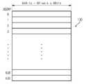
도 7은 도 4에 도시된 라인 메모리(130)의 바람직한 실시예를 보여주고 있다. 도 7에 도시된 라인 메모리(130)는 0부터 639까지의 어드레스 신호(ADDRP)에 의해서 지정될 수 있는 640 개의 어드레스 공간을 갖는다. 각 어드레스 공간의 데이터 폭은 (8픽셀*8비트)=64비트이다. 따라서, 라인 메모리(130)의 크기는 8*8*640 비트이고, 한 페이즈 내 80 블록의 화상 데이터를 저장할 수 있다.FIG. 7 shows a preferred embodiment of the
라인 메모리(130)는 어드레스 발생기(140)로부터의 독출 인에이블 신호(REN)와 어드레스 신호(ADDRP)에 응답해서 저장된 데이터 세그먼트(PELO_P[63:0])를 출력한다. 라인 메모리(130)로부터 출력되는 일련의 데이터 세그먼트들은 블록 스캔 순서이다.The
분리기(150)는 라인 메모리(130)로부터 출력되는 데이터 세그먼트(PELO_P[63:0])를 픽셀 단위 즉, 8-비트씩 분리해서 픽셀 데이터(PELO[7:0])를 출력한다. JPEG 엔진(160)은 분리기(150)로부터의 픽셀 데이터(PELO[7:0])를 받아들여서 내부 신호 처리를 수행한다.The
어드레스 발생 회로(140)는 라인 메모리(130)에 대한 공통 독출/기입 어드레스 신호(ADDRP)와 기입 인에이블 신호(WEN) 및 독출 인에이블 신호(REN)를 발생한 다. 본 발명의 바람직한 실시예에서 라인 메모리(140)에 대한 독출 어드레스와 기입 어드레스는 동일하다. 즉, 라인 메모리(130)의 어드레스(ADDRP)에 저장된 화상 데이터를 독출한 후 바로 그 어드레스(ADDRP)에 입력된 화상 데이터가 기입된다.The
구체적으로, 어드레스 발생기(140)는 아래 수학식 3과 같은 알고리즘을 이용하여 어드레스 신호(ADDRP)를 발생한다.Specifically, the
no_size = (no_hor_bk << 3) - 1;no_size = (no_hor_bk << 3)-1;
block_offset = 1;block_offset = 1;
line_offset = no_hor_bk;line_offset = no_hor_bk;
while (!finished){while (! finished) {
for (i=0; i<no_hor_bk; i++){ for (i = 0; i <no_hor_bk; i ++) {
for(v=0; v<8; v++){for (v = 0; v <8; v ++) {
addrp= (block_offset * i + line_offset * v) % no_size;addrp = (block_offset * i + line_offset * v)% no_size;
if (v==7 && i=no_hor_bk - 1) addrp = no_size;if (v == 7 && i = no_hor_bk-1) addrp = no_size;
dout_pack = M[addpr[; din_pack = 0;dout_pack = M [addpr [; din_pack = 0;
for (h=0; h<8; h++){for (h = 0; h <8; h ++) {
dout = dout_pack[63:56];dout = dout_pack [63:56];
din_pack = {din_pack <<8, din};din_pack = {din_pack << 8, din};
dout_pack = dout_pack<<;dout_pack = dout_pack <<;
}}
M{addrp] = din_pack;M {addrp] = din_pack;
}}
} }
block_offset = line_offset; block_offset = line_offset;
line_offset = (line_offset * no_hor_bk) % no_size; line_offset = (line_offset * no_hor_bk)% no_size;
}}
여기서, addrp은 어드레스 신호(ADDRP)이고, i는 블록 인덱스, v는 수직 방향 픽셀 인덱스(즉, 라인 인덱스) 그리고 h는 수평 방향 픽셀 인덱스이다. no_hor_bk는 한 페이즈에 속하는 블록의 갯수 H/h=640/8이고, no_size는 수평 방향 픽셀의 수-1를 나타낸다. 상기 수학식 3에서 640대신 다른 값을 사용하면 처리하고자 하는 한 프레임의 크기에 부합하는 어드레스 신호가 생성된다.Where addrp is an address signal ADDRP, i is a block index, v is a vertical pixel index (ie, a line index), and h is a horizontal pixel index. no_hor_bk is the number of blocks belonging to one phase, H / h = 640/8, and no_size represents the number of horizontal pixels-1. Using another value instead of 640 in
이와 같은 알고리즘에 의하여, 카메라 프로세서(110)로부터 공급되어서 조합기(120)에 의해 64-비트 데이터로 조합된 라스터 스캔 순서의 데이터 세그먼트(PELI_P[63:0])는 라인 메모리(130)에 저장된 후 블록 스캔 순서의 데이터 세그먼트(PELO_P[63:0])로 독출되어서 분리기(150)에 의해 한 픽셀 데이터씩 분리된 후 JPEG 엔진(160)으로 제공된다.By such an algorithm, the data segment PELI_P [63: 0] of raster scan order supplied from the
라스터 스캔 순서의 데이터 세그먼트(PELI_P[63:0])를 라인 메모리(130)에 저장한 후 블록 스캔 순서의 데이터 세그먼트(PELO_P[63:0])를 독출하기 위해서는 앞서 설명한 수학식 3의 알고리즘에 따라서 어드레스 신호(ADDRP)를 발생해야만 한다. 어드레스 발생기(140)에서 발생되는 어드레스 신호(ADDRP)에 대한 이해를 돕기 위하여 한 프레임의 크기가 80*32인 화상 데이터가 일 예로서 설명된다.After storing the data segment PELI_P [63: 0] of the raster scan order in the
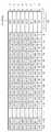
도 8은 카메라 프로세서(110)로부터 출력되는 화상 데이터를 보여준다. 도 8에서, 카메라 프로세서(110)의 수평 해상도는 80이고, 수직 해상도는 32인 것으로 가정하고, 또한, 라인 메모리(130)는 80*8 픽셀 화상 데이터를 저장할 수 있는 크기를 갖는다고 가정하면, 한 프레임은 4 개의 페이즈들(Phase1-Phase4)을 포함한다. 각 페이즈는 80 개의 세그먼트들(S0-S79)을 포함한다. 세그먼트들(S0-S79) 각각은 8 개의 픽셀들을 포함한다. 세그먼트들(S0-S79)의 각 숫자는 카메라 프로세서(110)로부터 출력되는 화상 데이터의 순서를 의미한다.8 shows image data output from the
도 9a 내지 도 9d는 조합기(120)로부터 출력되는 한 페이즈의 데이터 세그먼트들이 라인 메모리(130)에 기입된 예들을 보여주는 도면들이고, 도 10a 및 도 10b는 데이터 세그먼트들이 라인 메모리(130)로부터/에 독출/기입될 때 신호들의 타이밍도들이다.9A-9D are diagrams showing examples in which one phase of data segments output from the
먼저 도 9a 및 도 10a를 참조하여, 페이즈1(Phase 1)의 데이터 세그먼트들이 라인 메모리(130)에 저장되는 방법이 설명된다. 조합기(120)는 카메라 프로세서(110)로부터 출력되는 페이즈1(Phase 1)에 속하는 픽셀 데이터(PELI[7:0])를 8개씩 조합하여 데이터 세그먼트(PELI_P[63:0])를 생성한다. 조합기(120)는 클럭 신호 (CLK)의 8 주기마다 생성된 데이터 세그먼트(PELI_P[63:0])를 출력한다. 조합기(120)로부터 출력되는 데이터 세그먼트(PELI_P[63:0])는 라인 스캔 순서이다.First, referring to FIGS. 9A and 10A, a method of storing data segments of
어드레스 발생기(140)는 8 클럭 사이클마다 기입 인에이블 신호(WEN)를 활성화하며, 어드레스 신호(ADDRP)를 발생한다. 어드레스 신호(ADDRP) 발생 알고리즘은 앞서 설명한 수학식 3과 같다. 도 9a에 도시된 실시예에서, 어드레스 발생기(140)에 의해 발생되는 어드레스 신호(ADDRP)는 0, 1, 2, 3, …, 78, 79 순이다.The
라인 메모리(130)는 기입 인에이블 신호(WEN)와 어드레스 신호(ADDRP)에 응답해서 조합기(120)로부터 출력되는 데이터 세그먼트들(S0-S79)을 순차적으로 저장한다. 그러므로, 라인 메모리(130)의 어드레스들 0, 1, 2, 3, 4, …, 78, 79 각각에는 세그먼트 S0, S1, S2, S3, S4, …, S78, S79이 저장된다. 도 9a에서, 빗금친 부분은 다음 도 9b에서 설명될 페이즈 2에 속하는 세그먼트들에 대한 기입 동작과 함께 페이즈 1에 속하는 세그먼트들에 대한 블록 스캔 순서로 독출될 첫 번째 블록(8*8)이다.The
도 9b는 라인 메모리(130)로부터 페이즈 1에 속하는 데이터 세그먼트들에 대한 독출 동작과 아울러 페이즈 2에 속하는 데이터 세그먼트들에 대한 기입 동작이 완료되었을 때 라인 메모리(130)에 저장된 페이즈 2에 속하는 데이터 세그먼트들을 보여주고 있다.9B shows a data segment belonging to
도 9b 및 도 10b를 참조하면, 어드레스 발생기(140)에서 발생되는 어드레스 신호(ADDRP)는 0, 10, 20, 30 … 70, 1 … 71, …, 9 …79 순이다. 그러므로, 라인 메모리(130)로부터 독출되는 데이터 세그먼트는, 페이즈1(Phase 1)에 속하는 데 이터 세그먼트 S0, S10, S20 … S70, S1 … S71, …, S9 …S79 순이다. 이는 도 9a를 참조하면 쉽게 이해 될 수 있으며, 라인 메모리(130)로부터 출력되는 데이터 세그먼트는 블록 스캔 순서이다. 독출 인에이블 신호(REN)가 활성화된 후 기입 인에이블 신호(WEN)가 활성화되므로, 어드레스 신호(ADDRP)가 0일 때, 라인 메모리(130)는 독출 인에이블 신호(REN)에 응답해서 페이즈1(Phase 1)의 세그먼트 S0를 출력한 후, 기입 인에이블 신호(WEN)에 응답해서 페이즈2(Phase 2)의 세그먼트 S0를 저장한다. 이와 같은 방법으로, 페이즈1(Phase 1)에 속하는 세그먼트들이 라인 메모리(130)로부터 순차적으로 독출되며, 또한 페이즈2(Phase 2)에 속하는 세그먼트들이 라인 메모리(130)에 순차적으로 저장된다. 도 9b에서, 빗금친 부분은 다음 도 9c에서 설명될 페이즈 3에 속하는 세그먼트들에 대한 기입 동작과 함께 페이즈 2에 속하는 세그먼트들에 대한 블록 스캔 순서로 독출될 첫 번째 블록(8*8)이다.9B and 10B, the address signal ADDRP generated by the
도 9c는 라인 메모리(130)로부터 페이즈 2에 속하는 데이터 세그먼트들에 대한 독출 동작과 아울러 페이즈 3에 속하는 데이터 세그먼트들에 대한 기입 동작이 완료되었을 때 라인 메모리(130)에 저장된 페이즈 3에 속하는 데이터 세그먼트들을 보여주고 있다.9C shows a data segment belonging to
도 9c를 참조하면, 어드레스 발생기(140)에서 발생되는 어드레스 신호(ADDRP)는 0, 21, 42, 63 … 68, 10 … 78, …, 11 …79 순이다. 그러므로, 라인 메모리(130)로부터 독출되는 데이터 세그먼트는, 페이즈2(Phase 2)에 속하는 데이터 세그먼트 S0, S10, S20 … S70, S1 … S71, …, S9 …S79 순이다. 이는 도 9b를 참조하면 쉽게 이해 될 수 있으며, 라인 메모리(130)로부터 출력되는 데이터 세 그먼트는 블록 스캔 순서이다.Referring to FIG. 9C, the address signal ADDRP generated by the
도 9d는 라인 메모리(130)로부터 페이즈 3에 속하는 데이터 세그먼트들에 대한 독출 동작과 아울러 페이즈 4에 속하는 데이터 세그먼트들에 대한 기입 동작이 완료되었을 때 라인 메모리(130)에 저장된 페이즈 4에 속하는 데이터 세그먼트들을 보여주고 있다.9D shows a data segment belonging to
도 9d를 참조하면, 어드레스 발생기(140)에서 발생되는 어드레스 신호(ADDRP)는 0, 52, 25, 77 … 48, 21 … 69, …, 31 …79 순이다. 그러므로, 라인 메모리(130)로부터 독출되는 데이터 세그먼트는, 페이즈3(Phase 3)에 속하는 데이터 세그먼트 S0, S10, S20 … S70, S1 … S71, …, S9 …S79 순이다. 이는 도 9c를 참조하면 쉽게 이해 될 수 있으며, 라인 메모리(130)로부터 출력되는 데이터 세그먼트는 블록 스캔 순서이다.9D, the address signals ADDRP generated by the
상술한 바와 같은 본 발명의 바람직한 실시예에 따르면, 카메라 프로세서(110)로부터 출력되는 8-비트 픽셀 데이터(PELI[7:0])는 조합기(120)에 의해서 64 비트씩 조합된다. 픽셀 데이터 단위가 아닌 조합된 데이터 세그먼트(PELI_P[63:0) 단위로 라인 메모리(130)가 액세스되므로 라인 메모리(130) 액세스에 수반되는 전력 소비량이 감소된다.According to a preferred embodiment of the present invention as described above, the 8-bit pixel data PELI [7: 0] output from the
도 11은 해상도가 VGA인 경우 컬러 성분 데이터를 라인 메모리에 저장할 때 0.13um에서의 전력 소비량을 보여주고 있다.FIG. 11 shows power consumption at 0.13 um when color component data is stored in the line memory when the resolution is VGA.
어드레스 신호(ADDRP)를 발생하는 알고리즘의 다른 예들이 아래 수학식 4 및 수학식 5에 기재되어 있다.Other examples of the algorithm for generating the address signal ADDRP are described in
no_size = (no_hor_bk<<3) - 1;no_size = (no_hor_bk << 3)-1;
block_offset = 1;block_offset = 1;
line_offset = no_hor_bk;line_offset = no_hor_bk;
while (!finished){while (! finished) {
block_number = 0; block_number = 0;
for (i=0; i<no_hor_bk; i++){ for (i = 0; i <no_hor_bk; i ++) {
line_number = 0; line_number = 0;
for (v=0; v<8; v++){ for (v = 0; v <8; v ++) {
addrp = (block_number + line_number); addrp = (block_number + line_number);
if (addrp>=no_size) addrp -= no_size; if (addrp> = no_size) addrp-= no_size;
if (v==7 && i=no_hor_bk-1) addrp = no_size; if (v == 7 && i = no_hor_bk-1) addrp = no_size;
dout_pack = M[addrp]; din_pack = 0; dout_pack = M [addrp]; din_pack = 0;
for (h=0; h<8; h++) { for (h = 0; h <8; h ++) {
dout = dout_pack[63:56]; dout = dout_pack [63:56];
din_pack = {din_pack<<8,din}; din_pack = {din_pack << 8, din};
dout_pack = dout_pack<<8; dout_pack = dout_pack << 8;
} }
M[addrp] = din_pack; M [addrp] = din_pack;
line_number += line_offset; line_number + = line_offset;
if (line_number>=no_size) line_number -= no_size; if (line_number> = no_size) line_number-= no_size;
} }
block_number += block_offset; block_number + = block_offset;
if (block_number>=no_size) block_number -= no_size; if (block_number> = no_size) block_number-= no_size;
} }
block_offset = line_offset; block_offset = line_offset;
line_offset = (line_offset * no_hor_bk) % no_size; line_offset = (line_offset * no_hor_bk)% no_size;
} }
block_offset = 1;block_offset = 1;
line_offset = no_hor_bk;line_offset = no_hor_bk;
while (!finished){while (! finished) {
addrp = 0; addrp = 0;
block_number = 0; block_number = 0;
for (i=0; i<no_hor_bk; i++){ for (i = 0; i <no_hor_bk; i ++) {
line_number = 0; line_number = 0;
for (v=0; v<8; v++){ for (v = 0; v <8; v ++) {
if (addrp>=no_size) addrp -= no_size; if (addrp> = no_size) addrp-= no_size;
if (v==7 && i=no_hor_bk-1) addrp = no_size; if (v == 7 && i = no_hor_bk-1) addrp = no_size;
dout_pack = M[addrp]; din_pack = 0; dout_pack = M [addrp]; din_pack = 0;
for (h=0; h<8; h++) { for (h = 0; h <8; h ++) {
dout = dout_pack[63:56]; dout = dout_pack [63:56];
din_pack = {din_pack<<8,din}; din_pack = {din_pack << 8, din};
dout_pack = dout_pack<<8; dout_pack = dout_pack << 8;
} }
M[addrp] = din_pack; M [addrp] = din_pack;
line_number += line_offset; line_number + = line_offset;
if (line_number>=no_size) line_number -= no_size; if (line_number> = no_size) line_number-= no_size;
addrp = (block_number + line_number); addrp = (block_number + line_number);
if (addrp>=no_size) addrp -= no_size; if (addrp> = no_size) addrp-= no_size;
} }
block_number += block_offset; block_number + = block_offset;
if (block_number>=no_size) block_number -= no_size; if (block_number> = no_size) block_number-= no_size;
} }
block_offset = line_offset; block_offset = line_offset;
line_offset = (line_offset * no_hor_bk) % no_size; line_offset = (line_offset * no_hor_bk)% no_size;
} }
수학식 3의 알고리즘의 3 개의 승산기를 필요로 하나, 수학식 4의 알고리즘에 의하면, 승산기가 불필요하다. 또한, 효율적인 하드웨어 구현을 위해서 어드레스 신호(addrp)를 생성하는 부분을 수학식 5의 알고리즘과 같이 수정할 수 있다.Three multipliers of the algorithm of
한편, 본 발명은 다수의 성분을 가진 칼라 신호에 대응하기 위하여 특정한 크로마 포맷(chroma format)(예컨대, 4:2:2, 4:4:4 등)에 적합하도록 라인 메모리의 크기는 변경될 수 있다. 예를 들어, 4:2:2 포맷의 경우 라인 메모리의 크기는 H*2*8이 되며, 4:4:4 포맷의 경우 라인 메모리의 크기는 H*3*8이 된다.Meanwhile, the present invention can change the size of the line memory so as to conform to a specific chroma format (eg, 4: 2: 2, 4: 4: 4, etc.) in order to correspond to a color signal having a plurality of components. have. For example, in the 4: 2: 2 format, the line memory size is H * 2 * 8, and in the 4: 4: 4 format, the line memory size is H * 3 * 8.
예시적인 바람직한 실시예를 이용하여 본 발명을 설명하였지만, 본 발명의 범위는 개시된 실시예에 한정되지 않는다는 것이 잘 이해될 것이다. 따라서, 청구범위는 그러한 변형 예들 및 그 유사한 구성들 모두를 포함하는 것으로 가능한 폭넓게 해석되어야 한다.While the invention has been described using exemplary preferred embodiments, it will be understood that the scope of the invention is not limited to the disclosed embodiments. Accordingly, the claims should be construed as broadly as possible to cover all such modifications and similar constructions.
이와 같은 본 발명에 의하면, 색 성분마다 하나의 라인 메모리를 사용하므로서 라인 메모리 크기가 감소된다. 따라서, 칩에 내장시 작은 크기의 칩을 얻을 수 있다. 더욱이, 본 발명은 8 픽셀 데이터 조합인 데이터 세그먼트 단위로 라인 메모리를 액세스하므로, 픽셀 데이터 단위로 라인 메모리를 액세스하는 것에 비해 전력 소모가 적다.According to the present invention as described above, the line memory size is reduced by using one line memory for each color component. Thus, a small size chip can be obtained when embedded in the chip. Furthermore, the present invention accesses the line memory in data segment units, which is a combination of 8 pixel data, and therefore consumes less power than accessing the line memory in pixel data units.
Claims (24)
Translated fromKoreanPriority Applications (3)
| Application Number | Priority Date | Filing Date | Title |
|---|---|---|---|
| KR20040091505AKR100614652B1 (en) | 2004-11-10 | 2004-11-10 | Image processing apparatus and method with reduced power consumption |
| US11/151,151US20060098012A1 (en) | 2004-11-10 | 2005-06-13 | Apparatus and method for processing image with reduced memory capacity and power consumption |
| JP2005310198AJP2006141001A (en) | 2004-11-10 | 2005-10-25 | Image processing apparatus and method with reduced power consumption |
Applications Claiming Priority (1)
| Application Number | Priority Date | Filing Date | Title |
|---|---|---|---|
| KR20040091505AKR100614652B1 (en) | 2004-11-10 | 2004-11-10 | Image processing apparatus and method with reduced power consumption |
Publications (2)
| Publication Number | Publication Date |
|---|---|
| KR20060042740A KR20060042740A (en) | 2006-05-15 |
| KR100614652B1true KR100614652B1 (en) | 2006-08-22 |
Family
ID=36315842
Family Applications (1)
| Application Number | Title | Priority Date | Filing Date |
|---|---|---|---|
| KR20040091505AExpired - Fee RelatedKR100614652B1 (en) | 2004-11-10 | 2004-11-10 | Image processing apparatus and method with reduced power consumption |
Country Status (3)
| Country | Link |
|---|---|
| US (1) | US20060098012A1 (en) |
| JP (1) | JP2006141001A (en) |
| KR (1) | KR100614652B1 (en) |
Families Citing this family (2)
| Publication number | Priority date | Publication date | Assignee | Title |
|---|---|---|---|---|
| CN108293121B (en)* | 2015-11-24 | 2021-04-23 | 三星电子株式会社 | Video decoding method and device and encoding method and device |
| JP6757141B2 (en)* | 2016-01-18 | 2020-09-16 | キヤノン株式会社 | Image processing device, its control method, and program |
Family Cites Families (6)
| Publication number | Priority date | Publication date | Assignee | Title |
|---|---|---|---|---|
| KR100207705B1 (en)* | 1996-12-04 | 1999-07-15 | 윤종용 | Apparatus and method of addressing for dct block and raster scan |
| JP2001285644A (en)* | 2000-03-31 | 2001-10-12 | Sony Corp | Control method for line memory |
| AUPR192800A0 (en)* | 2000-12-06 | 2001-01-04 | Canon Kabushiki Kaisha | Digital image compression and decompression |
| JP4015890B2 (en)* | 2002-06-28 | 2007-11-28 | 松下電器産業株式会社 | Pixel block data generation apparatus and pixel block data generation method |
| US7379609B2 (en)* | 2002-07-19 | 2008-05-27 | Samsung Electronics Co., Ltd. | Image processing apparatus and method for conversion between raster and block formats |
| KR100502413B1 (en)* | 2002-11-07 | 2005-07-19 | 삼성전자주식회사 | Image processing apparatus and method for converting image data between raster scan order and block scan order |
- 2004
- 2004-11-10KRKR20040091505Apatent/KR100614652B1/ennot_activeExpired - Fee Related
- 2005
- 2005-06-13USUS11/151,151patent/US20060098012A1/ennot_activeAbandoned
- 2005-10-25JPJP2005310198Apatent/JP2006141001A/enactivePending
Also Published As
| Publication number | Publication date |
|---|---|
| KR20060042740A (en) | 2006-05-15 |
| US20060098012A1 (en) | 2006-05-11 |
| JP2006141001A (en) | 2006-06-01 |
Similar Documents
| Publication | Publication Date | Title |
|---|---|---|
| KR100794307B1 (en) | Image processing apparatus and method | |
| US5920343A (en) | Imaging system with image processing for re-writing a portion of a pixel block | |
| EP0828238A2 (en) | Image memory storage system and method for a block oriented image processing system | |
| KR100502413B1 (en) | Image processing apparatus and method for converting image data between raster scan order and block scan order | |
| US20040100661A1 (en) | Pixel block data generating device and pixel block data generating method | |
| JP2002508909A (en) | Memory-based VLSI architecture for image compression | |
| KR100451584B1 (en) | Device for encoding and decoding a moving picture using of a wavelet transformation and a motion estimation | |
| US20020080880A1 (en) | Effective motion estimation for hierarchical search | |
| JP4628647B2 (en) | On-the-fly transfer of data between RGB and YCrCb color space for DCT interface | |
| KR100614652B1 (en) | Image processing apparatus and method with reduced power consumption | |
| US6542429B2 (en) | Method of controlling line memory | |
| EP0820199B1 (en) | Image signal processing apparatus and method | |
| US8732363B2 (en) | Data processing apparatus and data processing method | |
| US9021162B2 (en) | Data packet generation apparatus and data packet generation method | |
| JP2007158550A (en) | Image processing apparatus and image processing method | |
| KR100353894B1 (en) | Memory architecture for buffering jpeg input data and addressing method thereof | |
| JP3710066B2 (en) | Electronic still video camera | |
| JP5738639B2 (en) | Data processing apparatus and data processing method | |
| JP3530371B2 (en) | Image processing device | |
| JP2002354400A (en) | Data storage / readout method, image data storage device using the method, and image correction device using the storage device | |
| JP3352346B2 (en) | Image signal processing device | |
| TW200838311A (en) | Method for buffering output pixel data of a JPEG image | |
| JP6242417B2 (en) | Data processing apparatus and data processing method | |
| JPH04104692A (en) | Image data transfer control method | |
| KR19980075855A (en) | Method and device for controlling frame memory for compressing video signal |
Legal Events
| Date | Code | Title | Description |
|---|---|---|---|
| A201 | Request for examination | ||
| PA0109 | Patent application | St.27 status event code:A-0-1-A10-A12-nap-PA0109 | |
| PA0201 | Request for examination | St.27 status event code:A-1-2-D10-D11-exm-PA0201 | |
| PN2301 | Change of applicant | St.27 status event code:A-3-3-R10-R13-asn-PN2301 St.27 status event code:A-3-3-R10-R11-asn-PN2301 | |
| PN2301 | Change of applicant | St.27 status event code:A-3-3-R10-R13-asn-PN2301 St.27 status event code:A-3-3-R10-R11-asn-PN2301 | |
| PG1501 | Laying open of application | St.27 status event code:A-1-1-Q10-Q12-nap-PG1501 | |
| E701 | Decision to grant or registration of patent right | ||
| PE0701 | Decision of registration | St.27 status event code:A-1-2-D10-D22-exm-PE0701 | |
| GRNT | Written decision to grant | ||
| PR0701 | Registration of establishment | St.27 status event code:A-2-4-F10-F11-exm-PR0701 | |
| PR1002 | Payment of registration fee | St.27 status event code:A-2-2-U10-U11-oth-PR1002 Fee payment year number:1 | |
| PG1601 | Publication of registration | St.27 status event code:A-4-4-Q10-Q13-nap-PG1601 | |
| LAPS | Lapse due to unpaid annual fee | ||
| PC1903 | Unpaid annual fee | St.27 status event code:A-4-4-U10-U13-oth-PC1903 Not in force date:20090815 Payment event data comment text:Termination Category : DEFAULT_OF_REGISTRATION_FEE | |
| PC1903 | Unpaid annual fee | St.27 status event code:N-4-6-H10-H13-oth-PC1903 Ip right cessation event data comment text:Termination Category : DEFAULT_OF_REGISTRATION_FEE Not in force date:20090815 | |
| R18-X000 | Changes to party contact information recorded | St.27 status event code:A-5-5-R10-R18-oth-X000 |