KR100613182B1 - Multilayer substrate and method of providing relaxed SiSi layer and SiSi / Si hetero structure on insulator - Google Patents
Multilayer substrate and method of providing relaxed SiSi layer and SiSi / Si hetero structure on insulatorDownload PDFInfo
- Publication number
- KR100613182B1 KR100613182B1KR1020037005157AKR20037005157AKR100613182B1KR 100613182 B1KR100613182 B1KR 100613182B1KR 1020037005157 AKR1020037005157 AKR 1020037005157AKR 20037005157 AKR20037005157 AKR 20037005157AKR 100613182 B1KR100613182 B1KR 100613182B1
- Authority
- KR
- South Korea
- Prior art keywords
- layer
- way
- sige
- substrate
- relaxed
- Prior art date
- Legal status (The legal status is an assumption and is not a legal conclusion. Google has not performed a legal analysis and makes no representation as to the accuracy of the status listed.)
- Expired - Fee Related
Links
Images


Classifications
- H—ELECTRICITY
- H01—ELECTRIC ELEMENTS
- H01L—SEMICONDUCTOR DEVICES NOT COVERED BY CLASS H10
- H01L21/00—Processes or apparatus adapted for the manufacture or treatment of semiconductor or solid state devices or of parts thereof
- H01L21/02—Manufacture or treatment of semiconductor devices or of parts thereof
- H01L21/04—Manufacture or treatment of semiconductor devices or of parts thereof the devices having potential barriers, e.g. a PN junction, depletion layer or carrier concentration layer
- H01L21/18—Manufacture or treatment of semiconductor devices or of parts thereof the devices having potential barriers, e.g. a PN junction, depletion layer or carrier concentration layer the devices having semiconductor bodies comprising elements of Group IV of the Periodic Table or AIIIBV compounds with or without impurities, e.g. doping materials
- H01L21/20—Deposition of semiconductor materials on a substrate, e.g. epitaxial growth solid phase epitaxy
- H—ELECTRICITY
- H01—ELECTRIC ELEMENTS
- H01L—SEMICONDUCTOR DEVICES NOT COVERED BY CLASS H10
- H01L21/00—Processes or apparatus adapted for the manufacture or treatment of semiconductor or solid state devices or of parts thereof
- H01L21/70—Manufacture or treatment of devices consisting of a plurality of solid state components formed in or on a common substrate or of parts thereof; Manufacture of integrated circuit devices or of parts thereof
- H01L21/71—Manufacture of specific parts of devices defined in group H01L21/70
- H01L21/76—Making of isolation regions between components
- H01L21/762—Dielectric regions, e.g. EPIC dielectric isolation, LOCOS; Trench refilling techniques, SOI technology, use of channel stoppers
- H01L21/7624—Dielectric regions, e.g. EPIC dielectric isolation, LOCOS; Trench refilling techniques, SOI technology, use of channel stoppers using semiconductor on insulator [SOI] technology
- H01L21/76251—Dielectric regions, e.g. EPIC dielectric isolation, LOCOS; Trench refilling techniques, SOI technology, use of channel stoppers using semiconductor on insulator [SOI] technology using bonding techniques
- H01L21/76256—Dielectric regions, e.g. EPIC dielectric isolation, LOCOS; Trench refilling techniques, SOI technology, use of channel stoppers using semiconductor on insulator [SOI] technology using bonding techniques using silicon etch back techniques, e.g. BESOI, ELTRAN
- H—ELECTRICITY
- H01—ELECTRIC ELEMENTS
- H01L—SEMICONDUCTOR DEVICES NOT COVERED BY CLASS H10
- H01L21/00—Processes or apparatus adapted for the manufacture or treatment of semiconductor or solid state devices or of parts thereof
- H01L21/02—Manufacture or treatment of semiconductor devices or of parts thereof
- H01L21/04—Manufacture or treatment of semiconductor devices or of parts thereof the devices having potential barriers, e.g. a PN junction, depletion layer or carrier concentration layer
- H01L21/18—Manufacture or treatment of semiconductor devices or of parts thereof the devices having potential barriers, e.g. a PN junction, depletion layer or carrier concentration layer the devices having semiconductor bodies comprising elements of Group IV of the Periodic Table or AIIIBV compounds with or without impurities, e.g. doping materials
- H01L21/20—Deposition of semiconductor materials on a substrate, e.g. epitaxial growth solid phase epitaxy
- H01L21/2003—Deposition of semiconductor materials on a substrate, e.g. epitaxial growth solid phase epitaxy characterised by the substrate
- H01L21/2007—Bonding of semiconductor wafers to insulating substrates or to semiconducting substrates using an intermediate insulating layer
Landscapes
- Engineering & Computer Science (AREA)
- Microelectronics & Electronic Packaging (AREA)
- Condensed Matter Physics & Semiconductors (AREA)
- General Physics & Mathematics (AREA)
- Manufacturing & Machinery (AREA)
- Computer Hardware Design (AREA)
- Physics & Mathematics (AREA)
- Power Engineering (AREA)
- Recrystallisation Techniques (AREA)
- Element Separation (AREA)
- Bipolar Transistors (AREA)
- Junction Field-Effect Transistors (AREA)
- Thin Film Transistor (AREA)
Abstract
Translated fromKoreanDescription
Translated fromKorean본 발명은 SiGe 층을 제 2 기판에 전사하며, 미세 전자 공학 및 광전자 공학에서의 신규 애플리케이션을 가지는 새로운 물질 구조를 형성하는 것에 관한 것이다. 특히, 절연체 구조 상의 변형 Si/SiGe 층은 상보성 금속 산화물 반도체(complementary metal oxide semiconductor, CMOS) 트랜지스터, 조절 도핑된 전계 효과 트랜지스터(MODFETs), 높은 전자 이동도 트랜지스터(HEMTs) 및 바이폴라 트랜지스터(BTs)와 같은 고속 장치(high speed device)를 제조하는데 유용하며, Si 상의 SiGe 층 헤테로 구조는 통신, 감시(surveillance) 및 의료 애플리케이션을 위한 Si형 초 적외선(far infrared)을 제공하는 광검파기(photodetector)를 제조하는데 사용될 수 있다.The present invention relates to transferring a SiGe layer to a second substrate and forming a new material structure with new applications in microelectronics and optoelectronics. In particular, the strained Si / SiGe layer on the insulator structure is comprised of complementary metal oxide semiconductor (CMOS) transistors, regulated doped field effect transistors (MODFETs), high electron mobility transistors (HEMTs) and bipolar transistors (BTs). Useful for manufacturing such high speed devices, the SiGe layer heterostructure on Si fabricates a photodetector that provides Si-type far infrared for communication, surveillance and medical applications. It can be used to
미세 전자 공학에서의 애플리케이션의 경우, 높은 캐리어 이동도가 바람직하다. 변형 Si/SiGe 채널에서의 전자 이동도는 벌크 Si에서의 전자 이동도보다 상당히 높은 것으로 밝혀졌다. 예를 들면, 상온에서 측정된 변형 Si에서의 전자 이동 도의 값은 벌크 Si에서의 400cm2/Vs에 비하여 약 3000cm2/Vs정도 된다. 유사하게, 높은 Ge 농도(60%~80%)를 가지는 변형 SiGe에서의 정공 이동도(hole mobility)는 800cm2/Vs에 달하는 것으로, 이는 벌크 Si에서의 정공 이동도인 150cm2/Vs의 약 5배의 값이 된다. 현재 기술 수준의 Si 장치에서 이 물질들을 사용하는 것은 훨씬 더 높은 성능, 특히 더 높은 동작 속도를 가져올 것으로 기대된다. 그러나, MODFET 및 HBT를 위한 하부 도통 기판 또는 하부 기판과 CMOS에서의 활성 장치 영역의 상호 작용은 고속 장치의 완전한 구현을 제한하는 바람직하지 않은 특징들이 된다. 이 문제를 해결하기 위해, SiGe 장치 층을 기판으로부터 격리하는 절연층이 제안된다. 따라서, 절연 물질 상에 변형 Si/SiGe를 제조할 수 있는 기술이 요구된다.For applications in microelectronics, high carrier mobility is desirable. The electron mobility in the strained Si / SiGe channel was found to be significantly higher than the electron mobility in bulk Si. For example, electromigration-degree value of the measured strain Si at room temperature is approximately 3000cm2 / Vs compared to 400cm2 / Vs in a bulk Si. Similarly, the hole mobility in the strained SiGe having a high Ge concentration (60% to 80%) is also (hole mobility) is 800cm2 / to Vs up to which the hole mobility in bulk Si also in 150cm2 / Vs about 5 times the value. The use of these materials in current state-of-the-art Si devices is expected to result in much higher performance, especially higher operating speeds. However, the interaction of the bottom conductive substrate or bottom substrate with the active device region in CMOS for MODFETs and HBTs is an undesirable feature that limits the complete implementation of high speed devices. In order to solve this problem, an insulating layer is proposed which isolates the SiGe device layer from the substrate. Thus, there is a need for a technique capable of producing strained Si / SiGe on insulating materials.
SiGe 온 절연체(SiGe-On-Insulator, SGOI)를 생성하기 위한 두 개의 이용 가능한 기술이 있다. 하나는 T. Mizuno 등에 의한 출판물 "High Performance Strained-Si p-MOSFETs on SiGe-On-Insulator Substrates Fabricated by SIMOX Technology," IEDM, 99-934에서 개시되는 것과 같은 SIMOX를 통한 기술이다. 그러나, 이 방법은 격자 불일치에 의해서 야기되는 기존의 결점에 더하여 산소 주입(oxygen implantation)은 완화된 SiGe 층에서 다른 손상을 유도하기 때문에 여러 가지 제한점을 가진다. 그리고, 산소 주입 이후에 산화물을 형성하는데 필요한 고온 어닐(>1100℃)은 변형 Si/SiGe 층에 불리한데, 그 이유는 Ge가 600℃를 초과하는 온도에서 확산하고 집적하는 경향이 있기 때문으로서, 이러한 것은 Ge 함유량이 10%를 초과할 경우에 보다 더 커지게 된다.There are two available techniques for producing SiGe-On-Insulators (SGOIs). One is a technique via SIMOX, such as disclosed in T. Mizuno et al., "High Performance Strained-Si p-MOSFETs on SiGe-On-Insulator Substrates Fabricated by SIMOX Technology," IEDM, 99-934. However, this method has several limitations, in addition to the existing defects caused by lattice mismatch, because oxygen implantation leads to other damage in the relaxed SiGe layer. And the high temperature annealing (> 1100 ° C.) needed to form the oxide after oxygen injection is disadvantageous for the strained Si / SiGe layer because Ge tends to diffuse and accumulate at temperatures above 600 ° C. This becomes larger when the Ge content exceeds 10%.
절연체 상에 SiGe를 제조하는 제 2 방법은 에칭 정지층(etch stop)의 도움을 통한 선택적 에칭 방법이다. 1999년 5월에 발행된 J. O. Chu와 K. E. Ismail에 의한 미국 특허 제 5,906,951호에는, KOH에서 p++ 도핑된 SiGe 에칭 정지층을 이용한 후면 웨이퍼 에칭을 이용하여 웨이퍼 본딩 및 SOI 기판 상에 변형 Si/SiGe의 층을 전사하는 방법이 개시되어 있다. 그러나, KOH에서 p++ 도핑된 SiGe 에칭 정지층에 대한 에칭 선택성은 에칭 정지층의 도핑 레벨이 1019/cm3 미만으로 될 때 급격히 감소하며, 따라서 p++SiGe 에칭 정지층에서 p++ 에칭 정지층에서의 도펀트의 변동에 기인하여 에칭이 균일하게 정지할 수 없다면, 변형 Si/SiGe 층 또한 KOH 에칭될 수 있다. 게다가, SiGe 에칭 정지층은 약 5×10¹⁹/cm3 내지 5×10²⁰/cm3 범위의 붕소로 강하게 도핑되기 때문에, 열 처리 동안에 변형 Si/SiGe의 자동 도핑될 가능성이 있다.A second method of producing SiGe on an insulator is a selective etching method with the aid of an etch stop. U.S. Patent No. 5,906,951 to JO Chu and KE Ismail, published May 1999, discloses a modified Si / wafer on SOI substrates using wafer bonding and back wafer etching using p++ doped SiGe etch stop layer. A method of transferring a layer of SiGe is disclosed. However, the etch selectivity for the SiGe etch stop layer in the p++ doped with KOH, and is rapidly decreased when the doping level of the etch stop layer is less than 1019 / cm3, thus p++ etch stop layer on the SiGe p++ If the etching cannot stop uniformly due to variations in the dopant in the etch stop layer, the strained Si / SiGe layer may also be KOH etched. In addition, since the SiGe etch stop layer is strongly doped with boron in the range of about 5 × 10¹⁹ / cm3 to 5 × 10²⁰ / cm3 , there is a possibility of automatic doping of strained Si / SiGe during heat treatment.
광섬유 애플리케이션의 경우, 300K에서 1.3㎛ 내지 1.6㎛ 광을 복조하기 위해서는 SiGe/Si 헤테로 접합 다이오드가 좋은 선택이 된다. 원하는 1.3㎛ 내지 1.6㎛ 파장에서의 흡수를 달성하는데 30% 내지 50% Ge의 사용이 제안되며, 광검파기 감도(photodetector sensitivity)를 향상시키는데 SiGe 층에서 디스로케이션(dislocation)과 같은 낮은 결함이 필요하다. 높은 응답성, 저잡음 및 빠른 응답을 가지는 SiGe/Si 헤테로 접합 다이오드를 달성하기 위한 현재 기술 수준의 기술은 100 주기 SiGe/Si 변형 층 초격자(superlattice)를 형성하기 위한 것이다. 그러나, 그 때 합금은 양자 크기 효과(quantum size effect)에 기인하여 더 이상 벌크 물질과 같이 작용하지 않는다. 양자 크기 효과의 순수 결과는 기대했던것 보다 짧은 파장(1.1㎛ 내지 1.3㎛)에서 흡수가 발생한다는 것이다. 그러므로, 1.3㎛ 내지 1.6㎛ 범위의 광을 흡수할 광검파기를 제조하기 위해서는 바람직한 Ge 함유량 및 낮은 결함을 가지는 벌크 SiGe 합금이 필요하다.For fiber optic applications, SiGe / Si heterojunction diodes are a good choice for demodulating 1.3 μm to 1.6 μm light at 300K. The use of 30% to 50% Ge is proposed to achieve the desired absorption at wavelengths of 1.3 μm to 1.6 μm and low defects such as dislocations in the SiGe layer are needed to improve the photodetector sensitivity. . Current state-of-the-art technology for achieving SiGe / Si heterojunction diodes with high responsiveness, low noise and fast response is to form a 100 cycle SiGe / Si strained layer superlattice. However, the alloy then no longer behaves like a bulk material due to the quantum size effect. The net result of the quantum size effect is that absorption occurs at shorter wavelengths (1.1 μm to 1.3 μm) than expected. Therefore, bulk SiGe alloys with desirable Ge content and low defects are needed to produce photodetectors that will absorb light in the range of 1.3 μm to 1.6 μm.
본 발명은 어떤 추가의 강하게 도핑된 에칭 정지층없이 에치백 방법을 사용하여 저결함 SiGe 층을 바람직한 기판 상으로 전사할 수 있는 방법을 제공하는 것이다. 본 발명의 핵심 특징은 SiGe 층이 에피택셜 변형 Si/SiGe를 성장시키는 층으로서 뿐만 아니라 일부의 특정 에칭 용액에서의 에칭 정지층으로서도 작용한다는 것이다. 다시 말해서, SiGe 층은 그러한 경우 자체 에칭 정지층이 된다. 그 결과, 절연체 상의 변형 Si/SiGe 또는 SiGe/Si 헤테로 구조를 제조하는 프로세스가 상당히 간략화되고, 변형 Si/SiGe 또는 SiGe/Si 헤테로 구조의 질이 상당히 향상된다.The present invention provides a method by which a low defect SiGe layer can be transferred onto a desired substrate using an etch back method without any further strongly doped etch stop layer. A key feature of the present invention is that the SiGe layer acts not only as a layer for growing epitaxially strained Si / SiGe but also as an etch stop layer in some specific etching solutions. In other words, the SiGe layer is in that case a self etch stop layer. As a result, the process for producing a strained Si / SiGe or SiGe / Si heterostructure on an insulator is considerably simplified, and the quality of the strained Si / SiGe or SiGe / Si heterostructure is significantly improved.
발명의 개요Summary of the Invention
본 발명에 따르면, 저결함 SiGe 벌크 층을 제 2 기판 상으로 전사하고, 절연체(SGOI) 또는 SiGe/Si 헤테로 구조 상에 변형 Si/SiGe를 형성하기 위한 방법이 개시된다. 이 방법은 반도체 기판을 선택하는 단계와, 그 반도체 기판 위에 제 1 에피택셜 단계형 Si1-xGex 층을 형성하는 단계와, 상기 제 1 에피택셜 단계형 Si1-xGex 층 위에 제 2 이완 Si1-yGey 층을 형성하는 단계와, 제 2 기판을 선택하는 단계와, 결합 기판을 형성하기 위해 상기 제 1 기판과 상기 제 2 기판을 본딩시키는 단계와, 상기 제 1 기판의 대다수를 제거하기 위해 그것의 후면으로부터 상기 제 1 기판을 그라인딩(grinding)하고 폴리싱(polishing)하는 단계와, 상기 제 1 기판의 잔여 물질을 에칭하고 SiGe 고선택성 습식(wet) 에칭 프로세스를 사용하여 Si1-xGex에서 정지하는 단계와, 상기 단계의 Si1-xGex층의 결함 불완전한 부분을 제거하기 위해 화학 기계 평탄화(chemical-mechanical planarization, CMP)를 적용하는 단계와, CMP 프로세스 단계에 의해 Si1-xGex층의 표면을 평탄화하는 단계와, 미세 전자 공학 애플리케이션을 위한 MOSFET, MODFET, HEMT 또는 BT용 Si1-xGex 층의 평탄화된 표면 위에 변형 Si/SiGe 층을 성장시키거나 또는 광전자 공학의 애플리케이션을 위한 SiGe 광검파기를 성장시키는 단계를 포함한다.According to the present invention, a method for transferring a low defect SiGe bulk layer onto a second substrate and forming strained Si / SiGe on an insulator (SGOI) or SiGe / Si heterostructure is disclosed. The method of claim on the first epitaxial step-type Si phase and the first epitaxial step-type Si1-x Gex layer to form the1-x Gex layer on the semiconductor substrate comprising the steps of: selecting a semiconductor substrate, Forming a two relaxed Si1-y Gey layer, selecting a second substrate, bonding the first substrate and the second substrate to form a bonded substrate, Grinding and polishing the first substrate from its back side to remove the majority, etching the remaining material of the first substrate and using a SiGe high selectivity wet etching process. the steps of, a CMP process, the method comprising applying a chemical mechanical planarization (chemical-mechanical planarization, CMP) to remove the defective defective part of the phase of the Si1-x Gex layer, which stops at the1-x Gex The surface of the Si1-x Gex layer by SiGe photodetectors for planarization and growing strained Si / SiGe layers on planarized surfaces of Si1-x Gex layers for MOSFETs, MODFETs, HEMTs or BTs for microelectronics applications, or for optoelectronics applications Growing a.
본 발명은 추가의 강하게 도핑된 에칭 정지층이 없이 에치백 방법을 사용하여 바람직한 기판 상에 저결함 SiGe 층을 전사하는 방법을 제공한다. 본 발명의 핵심 특징은 SiGe 층이 에피택셜 변형 Si/SiGe를 성장시키는 층으로서 뿐만 아니라 몇몇의 특정 에칭 용액에서 에칭 정지층 자체로서도 작용한다는 것이다. 즉, 이 경우에 SiGe 층은 자체 에칭 정지층(self-etch-stop)이 된다. 그 결과, 절연체 상의 변형 Si/SiGe 또는 SiGe/Si 헤테로 구조를 제조하는 프로세스가 상당히 간략화되며, 변형 Si/SiGe 또는 SiGe/Si 헤테로 구조의 질이 상당히 개선된다.The present invention provides a method of transferring a low defect SiGe layer onto a desired substrate using an etch back method without further heavily doped etch stop layer. A key feature of the present invention is that the SiGe layer acts not only as a layer for growing epitaxially strained Si / SiGe, but also as the etch stop layer itself in some specific etching solutions. That is, in this case the SiGe layer becomes a self-etch-stop. As a result, the process for producing a strained Si / SiGe or SiGe / Si heterostructure on an insulator is considerably simplified, and the quality of the strained Si / SiGe or SiGe / Si heterostructure is significantly improved.
본 발명은 후술에서, 비제한적인 실시예에 관하여 그리고 첨부 도면을 참조하여 더 상세히 설명된다.The invention is described in more detail below in connection with a non-limiting embodiment and with reference to the accompanying drawings.
도 1은 에피택셜적으로 성장된 단계형 Si1-xGex및 완화된 Si1-yGey 층을 가지는 제 1 기판의 단면도이다.1 is a cross- sectional view of a first substrate having epitaxially grown stepped Si1-x Gex and relaxed Si1-y Gey layers.
도 2는 절연체 층을 가지거나 가지지 않는 제 2 기판에 본딩되는 도 1에서 도시되는 제 1 반도체 기판의 단면도이다.FIG. 2 is a cross-sectional view of the first semiconductor substrate shown in FIG. 1 bonded to a second substrate with or without an insulator layer.
도 3은 그것의 후면으로부터 그라인딩하고 폴리싱함으로써 얇게되는 도 2에서 도시되는 제 1 기판의 단면도이다.3 is a cross-sectional view of the first substrate shown in FIG. 2 thinned by grinding and polishing from its backside.
도 4는 고선택성 습식 에칭 프로세스에 의해 단계형 Si1-xGex 층에서의 에칭과 정지의 단계 이후의 도 3에서 도시되는 제 1 기판의 잔여부의 단면도이다.4 is a cross- sectional view of the remainder of the first substrate shown in FIG. 3 after the step of etching and stopping in the stepped Si1-x Gex layer by a highly selective wet etching process.
도 5는 화학-기계 평탄화(CMP) 프로세스로써 도 4로부터 남아있는 Si1-xGex가 폴리싱되고 Si1-yGey 층이 평탄화되는 단면도이다.FIG. 5 is a sectional view in which the Si1-x Gex remaining from FIG. 4 is polished and the Si1-y Gey layer is planarized by a chemical-mechanical planarization (CMP) process.
도 6은 도 5에서 평탄화된 Si1-yGey위에 에피택셜적으로 성장되는 변형 Si/SiGe 층 또는 p-i-n 광검파기의 단면도이다.FIG. 6 is a cross- sectional view of a strained Si / SiGe layer or pin photodetector epitaxially grown over planarized Si1-y Gey in FIG. 5.
이상의 도면과 연계하여 이제 설명될 실시예는 표면의 평탄화와, 웨이퍼 본딩 및 에칭 정지층으로서 SiGe를 사용하는 선택적 습식 에칭 프로세스를 통해 절연체 물질 상에 단일 결정의 변형 Si/SiGe(SGOI)의 층 또는 Si 물질 상에 SiGe 층을 형성하는 것에 관한 것이다.Embodiments, which will now be described in conjunction with the above figures, include a layer of single crystal strain Si / SiGe (SGOI) on an insulator material, through a planarization of the surface and a selective wet etching process using SiGe as the wafer bonding and etch stop layer. And to form a SiGe layer on a Si material.
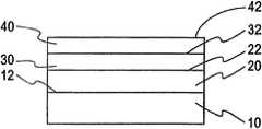
이제 도 1을 참조하면, 본 발명의 부분적 실시예의 단면도가 기판(10) 및 복수개의 층(20, 30, 40)을 포함하여 도시되어 있다. 기판(10)은 그 위에 에피택셜 층을 형성하기에 적합한 Si, SiGe, SiGeC, SiC 등과 같은 단일 결정의 층일 수 있다. Si1-xGex의 에피택셜 단계형 층(20)은 기판(10)의 상부 표면(12) 상에 형성된다. 단계형 층(20)의 상부 표면(22)은 실질상으로 완화되거나(relaxed) 또는 완전히 완화되어 있다. 완화는 1997년 8월 19일에 발행된 LeGoues 등의 미국 특허 제 5,659,187호에 개시되어 있는 변형된 프랑크-판독(Frank-Read) 메카니즘으로 기인할 수 있으며, 그 내용은 본 명세서에 참조로 인용되고 있다. 단계형 SiGe 층(20)을 형성하기 위한 방법은 LeGoures 등의 미국 특허 제 5,659,187호에서 개시되어 있다. 1994년 3월 29일에 발행된 B. S. Meyerson의 미국 특허 제 5,298,452호에서 설명되는 바와 같이 (후술될) 층(30)뿐만 아니라 층(20) 또한 UHV CVD 프로세스에서 형성될 수 있으며, 그 내용은 본 명세서에 참조로 인용되고 있다. 층(20)에서, Ge의 농도 x는 0부터 0.2 내지 0.5 범위의 값일 수 있다. 층(20)은 약 3,000 옹스트롬(300nm) 내지 1000nm의 범위의 두께를 가질 수 있다.Referring now to FIG. 1, a cross-sectional view of a partial embodiment of the present invention is shown including a
에피택셜 층(30)은 실질적으로 또는 완전히 완화된 Si1-yGey로 구성되고, 층(20)의 상부 표면(22) 상에 형성된다. 층(30)은 200nm 내지 1000nm 범위의 두께를 가질 수 있다. 층(30)에서의 Ge 함유량 y는 층(20)의 상부 표면(22)의 결정 격자 상수(the crystal lattice constant)와 일치하도록 선택되고, 그 결과 층(30)은 완화되거나 또는 본질적으로 변형이 없게된다. 층(30)에서의 Ge 함유량 y는 상부 표면(22)에서의 x의 값과 동일하거나 또는 대략 그 값일 수 있다. 값 y는 약 0.2 내지 약 0.5 범위 내일 수 있다. 밀봉 층(encapsulation layer)(40)이 완화 층(30) 위에 형성될 수도 있다. 밀봉 층(40)은 PECVD, LPDVD, UHV DVD 또는 스핀 온(spin-on) 기술을 통해 층(30)의 상부 표면(32) 상에 형성될 수 있다. 밀봉 층(40)은 상부 표면(42)을 가질 수 있다. 밀봉 물질은 가령, Si, SiO2, 폴리 Si, Si3N4, 낮은 k 유전체 물질 ―가령 다이아몬드형 탄소(Diamond Like Carbon, DLC), 플루오르 화합 다이아몬드형 탄소(Fluorinated Diamond Like Carbon, FDLC)―, Si, C, O 또는 H의 폴리머 또는 어떤 두 개 이상의 전술한 물질의 조합일 수 있다. Si, C, O 및 H의 폴리머의 일 예는 Grill 등에 의해 1998년 6월 29일에 출원되고 본 명세서에서 참조로 도입되어 있는 "Hydrogenated Oxidized Silicon Carbon Material"로 명명된 미국 특허 제 6,147,009호에 개시되어 있는 SiCOH이다. 층(40)을 형성하기 위한 증착 온도는 900℃ 미만일 수 있다. 밀봉 층의 두께는 약 5nm 내지 약 500nm 범위 내이다. 밀봉 층(40)은 층(30)의 상부 표면(32)을 보호하거나 격리 층을 제공하는 기능을 한다.The
도 2에서는, 제 2 기판(80)이 층(30)의 상부 표면(32) 또는 층(40)의 상부 표면(42)에 본딩된다. 웨이퍼 본딩 이전에, 층(30)의 표면(32) 또는 층(40)의 표면(42)은 화학 기계 평탄화(CMP) 프로세스에 의해 폴리싱되어 약 0.3nm 내지 약 1nm 범위 내의 루트 평균 제곱(RMS)으로의 표면 거칠기를 가지는 평면 표면이 되도록 표면(42)을 평탄화한다. 기판(80)은 Si, SiGe, SiGeC, SiC, 사파이어, 유리, 세라믹 또는 금속과 같은 반도체일 수 있고, 상부 표면(90)은 약 0.3nm 내지 약 1nm 범위의 RMS를 가지는 평탄한 상부 표면(90)을 제공하기 위해 이상과 같이 폴리싱될 수 있다.In FIG. 2, the
표면 거칠기를 감소시키기 위한 폴리싱에 대한 다른 설명을 위해 "A Method of Wafer Smoothing for Bonding Using Chemo-Mechanical Polishing(CMP)"(명세서 번호 YOR920000683US1)라 명명되고 본 명세서에 참조로 도입되어 있는 D. F. Canaperi 등에 의해 2000년 9월 29일에 출원된 번호 09/675841를 참조한다.For another description of polishing to reduce surface roughness, see DF Canaperi et al., Entitled " A Method of Wafer Smoothing for Bonding Using Chemo-Mechanical Polishing (CMP) ", specification No. YOR920000683US1, incorporated herein by reference. See number 09/675841, filed September 29, 2000.
본딩 구조를 제공하기 위한 본딩 웨이퍼에 대한 다른 설명을 위해, 본 명세서에 참조로 도입되어 있는 "Preparation of Strained Si/SiGe on Insulator by Hydrogen Induced Layer Transfer Technique"(명세서 번호 YOR920000345US1)라 명명된 D. F. Cnaperi 등에 의해 2000년 9월 29일에 출원된 번호 09/675840를 참조한다. 웨이퍼 본딩 및 H-주입 유도 층 전사에 의해 SGOI를 제조하는 방법은 특허 출원 제 09/675840호에 개시되어 있다. 이 방법은 종래 기술에 비해 절연체 상에 더 높은 Ge 함유량을 가지는 SiGe를 생성할 수 있다. 더 나아가, 종래 기술에 비해 이 방법은 비정합 디스로케이션의 제거에 기인하여 SiGe 층에서의 결함의 양을 감소시킬 수 있다. 그러나, 이 방법으로는, 전사된 SiGe 층이 상대적으로 얇으며(<1㎛), H의 주입 그리고 층 전달을 유도하기 위해 500℃ 내지 600℃에서 어닐링하는 것 때문에 높은 Ge 함유량의 층을 전사하는 것은 달성하기가 여전히 어렵다.For another description of bonding wafers for providing bonding structures, see DF Cnaperi et al., Entitled "Preparation of Strained Si / SiGe on Insulator by Hydrogen Induced Layer Transfer Technique" (spec. No. 09/675840, filed September 29, 2000, by reference. A method for producing SGOI by wafer bonding and H-injection induced layer transfer is disclosed in patent application 09/675840. This method can produce SiGe having a higher Ge content on the insulator as compared to the prior art. Furthermore, compared to the prior art, this method can reduce the amount of defects in the SiGe layer due to the elimination of mismatched dislocations. With this method, however, the transferred SiGe layer is relatively thin (<1 μm) and transfers a high Ge content layer due to annealing at 500 ° C. to 600 ° C. to induce injection and layer transfer of H. Is still difficult to achieve.
도 1에서 도시되어 있는 층(40)의 상부 표면(42)은 위쪽이 아래로 오도록 뒤집어져 기판(80)의 표면(90)과 접촉된다. 두 개의 표면(42, 90)은 웨이퍼 본딩법으로써 함께 본딩된다. 본딩된 표면(42, 90)은 약 2 시간 내지 약 50 시간 범위의 기간 동안 약 20℃ 내지 약 500℃ 범위의 온도에서 어닐링된다. 다른 실시예에서는 Ge 또는 금속 재료 등의 중간 층을 사용하는데, 이 금속 재료는 저융점을 갖거나 또는 실리콘과 반응하여 실리사이드를 형성하는 텅스텐(W), 코발트(Co), 티타늄(Ti) 등의 재료로서, 약 100℃ 내지 800℃ 범위의 어닐 온도에서의 고 접착력이 얻어진다. 어닐은 퍼니스 어닐(furnace aneal) 또는 빠른 열 어닐(RTA)일 수 있다.The
도 3은 그라인딩 또는 그라인딩과 폴리싱의 조합 프로세스를 이용하여 약 600㎛ 내지 약 750㎛ 범위의 제 1 기판(10)의 대부분을 제거한 것을 도시한다. 제 1 기판(10)의 남아 있는 층(70)은 약 50㎛ 내지 약 100㎛ 범위의 두께를 가진다.3 illustrates removal of most of the
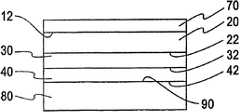
도 4는 약 90℃ 내지 약 120℃ 범위 온도에서의 에틸렌 다이아몬드(ethylenediamine), 파이로카테콜(pyrocatechol), 피라진(pyrazine), 물의 용액(EPPW 또는 EDP) 또는 약 70℃ 내지 약 85℃ 범위의 온도에서의 20% KOH의 용액 또는 TMAH(theramethly ammoniumhydroxide, (CH3)4NOH)의 다른 유기적 Si 에치 용액에서의 습식 에칭 프로세스로 층(70)을 제거하는 것을 도시한다. EPPW에서 Si1-yGey(y=0.15~0.3)에 대한 Si(100)의 에칭 선택성은 50 내지 1800 범위 내에 있도록 실험적으로 정해진다. KOH에서 Si1-yGey(y=0.2~0.3)에 대한 Si(100)의 에칭 선택성은 350 내지 1280 범위 내에 있도록 실험적으로 정해지고, Si1-yGey(y=0.2~0.3)에 대한 Si(100)의 에칭 선택성은 50 내지 115 범위 내에 있도록 실험적으로 정해진다. H. Naruse에게 1995년 12월 19일에 발행된 미국 특허 제 5,476,813호의 종래 기술에서는, SiGe 층에서 정지하는 동안 실리콘의 선택적 에칭을 위해 KOH, K2Cr2O7 및 프로파놀(propanol)의 혼합 용액이 사용된다. 그러나, 약 17 내지 20의 훨씬 더 낮은 선택성이 달성된다. 본 발명에서 EPPW, KOH 또는 TMAH는 Si1-yGey(y>0.1)에 비해 훨씬 더 높은 Si의 에칭률을 가져서 그 결과, J. O. Chu 등에게 1999년 5월 25일에 발행된 미국 특허 제 5,906,951에서 개시되어 있는 바와 같이 p++ SiGe 에칭 정지층과 같은 어떤 추가적 에칭 정지층 없이도 완화된 Si1-yGey에서 에칭 프로세스가 잘 정지한다.4 shows a solution of ethylene diamond (ethylenediamine), pyrocatechol, pyrazine, water (EPPW or EDP) or from about 70 ° C. to about 85 ° C. at temperatures ranging from about 90 ° C. to about 120 ° C. FIG. The removal of
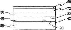
도 5는 계단-단계형 Si1-xGex 층(20)을 제거하기 위해 CMP 프로세스 단계를 적용한 이후의 절연체 상의 SiGe 층 또는 SiGe/Si 헤테로 구조의 단면도를 도시한다. 구조는 상부에 완화된 Si1-yGey 층(30)을 가진다. 단계형 Si1-xGex 층(20)을 제 거하고, 전사되어 완화된 Si1-yGey 층(30)의 두께를 조절하기 위해 화학 기계 평탄화(CMP) 프로세스가 사용된다. 변형 Si/SiGe를 에피택셜 성장시키거나 p-i-n 광검파기를 형성하기 위해 필요한 n+ Si층을 증착하기 위해 표면을 평탄화하고 세정하기 위해 최종 터치 폴리싱 및 세정이 사용된다.FIG. 5 shows a cross- sectional view of a SiGe layer or SiGe / Si heterostructure on an insulator after applying the CMP process step to remove the step-step Si1-x Gex layer 20. The structure has a relaxed Si1-y Gey layer 30 on top. A chemical mechanical planarization (CMP) process is used to remove the stepped Si1-x Gex layer 20 and to control the thickness of the transferred and relaxed Si1-y Gey layer 30. Final touch polishing and cleaning is used to planarize and clean the surface to deposit the n+ Si layer needed to epitaxially grow the strained Si / SiGe or form a pin photodetector.
도 6에서, 변형 Si/SiGe 또는 n+ Si의 층(60)은 SiGe 층(30) 위에서 에피택셜 성장하거나 형성된다. 변형 Si/SiGe 층의 에피택셜 성장에 대하여, 층(30) 위에 선택사양적 에피택셜 SiGe 버퍼 층(72)이 변형 Si/SiGe 층(60)의 성장 이전에 필요할 수 있다.In FIG. 6,
도면에서 유사한 요소 또는 구성요소들은 유사한 그리고 대응하는 참조 번호에 의해 참조된다는 것이 주목되어야 한다.It should be noted that similar elements or components in the figures are referred to by similar and corresponding reference numerals.
웨이퍼 본딩 및 습식 에칭을 사용하여 절연체 상의 SiGe(SGOI) 상의 변형 Si 또는 SiGe 또는 변형 SiGe/Si 헤테로 구조를 형성하기 위한 방법이 도시되고 설명되어 있지만, 본 명세서에 첨부되는 청구 범위의 범위에 의해서만 제한될 본 발명의 광범위로부터 벗어남이 없이 변경 및 변화가 가능하다는 것은 당업자들에게 명백할 것이다.
Although methods for forming strained Si or SiGe or strained SiGe / Si heterostructures on SiGe (SGOI) on insulators using wafer bonding and wet etching are shown and described, are only limited by the scope of the claims appended hereto. It will be apparent to those skilled in the art that modifications and variations are possible without departing from the broad scope of the present invention.
Claims (42)
Translated fromKoreanApplications Claiming Priority (3)
| Application Number | Priority Date | Filing Date | Title |
|---|---|---|---|
| US09/692,606 | 2000-10-19 | ||
| US09/692,606US6890835B1 (en) | 2000-10-19 | 2000-10-19 | Layer transfer of low defect SiGe using an etch-back process |
| PCT/GB2001/004159WO2002033746A1 (en) | 2000-10-19 | 2001-09-17 | Layer transfer of low defect sige using an etch-back process |
Publications (2)
| Publication Number | Publication Date |
|---|---|
| KR20030051714A KR20030051714A (en) | 2003-06-25 |
| KR100613182B1true KR100613182B1 (en) | 2006-08-17 |
Family
ID=24781275
Family Applications (1)
| Application Number | Title | Priority Date | Filing Date |
|---|---|---|---|
| KR1020037005157AExpired - Fee RelatedKR100613182B1 (en) | 2000-10-19 | 2001-09-17 | Multilayer substrate and method of providing relaxed SiSi layer and SiSi / Si hetero structure on insulator |
Country Status (9)
| Country | Link |
|---|---|
| US (4) | US6890835B1 (en) |
| EP (1) | EP1327263A1 (en) |
| JP (1) | JP2004512683A (en) |
| KR (1) | KR100613182B1 (en) |
| CN (1) | CN100472748C (en) |
| AU (1) | AU2001287881A1 (en) |
| IL (2) | IL155395A0 (en) |
| TW (1) | TW521395B (en) |
| WO (1) | WO2002033746A1 (en) |
Families Citing this family (82)
| Publication number | Priority date | Publication date | Assignee | Title |
|---|---|---|---|---|
| US7227176B2 (en)* | 1998-04-10 | 2007-06-05 | Massachusetts Institute Of Technology | Etch stop layer system |
| JP3883784B2 (en)* | 2000-05-24 | 2007-02-21 | 三洋電機株式会社 | Plate-shaped body and method for manufacturing semiconductor device |
| US6830976B2 (en) | 2001-03-02 | 2004-12-14 | Amberwave Systems Corproation | Relaxed silicon germanium platform for high speed CMOS electronics and high speed analog circuits |
| US6703688B1 (en) | 2001-03-02 | 2004-03-09 | Amberwave Systems Corporation | Relaxed silicon germanium platform for high speed CMOS electronics and high speed analog circuits |
| WO2002082514A1 (en) | 2001-04-04 | 2002-10-17 | Massachusetts Institute Of Technology | A method for semiconductor device fabrication |
| US6717213B2 (en)* | 2001-06-29 | 2004-04-06 | Intel Corporation | Creation of high mobility channels in thin-body SOI devices |
| JP2003249641A (en)* | 2002-02-22 | 2003-09-05 | Sharp Corp | Semiconductor substrate, method of manufacturing the same, and semiconductor device |
| US20030227057A1 (en) | 2002-06-07 | 2003-12-11 | Lochtefeld Anthony J. | Strained-semiconductor-on-insulator device structures |
| US6995430B2 (en) | 2002-06-07 | 2006-02-07 | Amberwave Systems Corporation | Strained-semiconductor-on-insulator device structures |
| US7074623B2 (en)* | 2002-06-07 | 2006-07-11 | Amberwave Systems Corporation | Methods of forming strained-semiconductor-on-insulator finFET device structures |
| JP2004014856A (en)* | 2002-06-07 | 2004-01-15 | Sharp Corp | Method for manufacturing semiconductor substrate and method for manufacturing semiconductor device |
| US7157119B2 (en) | 2002-06-25 | 2007-01-02 | Ppg Industries Ohio, Inc. | Method and compositions for applying multiple overlying organic pigmented decorations on ceramic substrates |
| US6936869B2 (en)* | 2002-07-09 | 2005-08-30 | International Rectifier Corporation | Heterojunction field effect transistors using silicon-germanium and silicon-carbon alloys |
| US7018910B2 (en) | 2002-07-09 | 2006-03-28 | S.O.I.Tec Silicon On Insulator Technologies S.A. | Transfer of a thin layer from a wafer comprising a buffer layer |
| US6841457B2 (en)* | 2002-07-16 | 2005-01-11 | International Business Machines Corporation | Use of hydrogen implantation to improve material properties of silicon-germanium-on-insulator material made by thermal diffusion |
| US6707106B1 (en)* | 2002-10-18 | 2004-03-16 | Advanced Micro Devices, Inc. | Semiconductor device with tensile strain silicon introduced by compressive material in a buried oxide layer |
| KR100874788B1 (en)* | 2003-01-07 | 2008-12-18 | 에스. 오. 이. 떼끄 씰리꽁 오 냉쉴라또흐 떼끄놀로지 | Recycling method by mechanical means of a wafer including a peeling structure after thin layer peeling |
| US20090325362A1 (en)* | 2003-01-07 | 2009-12-31 | Nabil Chhaimi | Method of recycling an epitaxied donor wafer |
| JP4659732B2 (en)* | 2003-01-27 | 2011-03-30 | 台湾積體電路製造股▲ふん▼有限公司 | Method for forming a semiconductor layer |
| US7049660B2 (en)* | 2003-05-30 | 2006-05-23 | International Business Machines Corporation | High-quality SGOI by oxidation near the alloy melting temperature |
| US6855963B1 (en)* | 2003-08-29 | 2005-02-15 | International Business Machines Corporation | Ultra high-speed Si/SiGe modulation-doped field effect transistors on ultra thin SOI/SGOI substrate |
| US7029980B2 (en) | 2003-09-25 | 2006-04-18 | Freescale Semiconductor Inc. | Method of manufacturing SOI template layer |
| FR2860340B1 (en) | 2003-09-30 | 2006-01-27 | Soitec Silicon On Insulator | INDIRECT BONDING WITH DISAPPEARANCE OF THE BONDING LAYER |
| JP2005109346A (en) | 2003-10-01 | 2005-04-21 | Seiko Epson Corp | Semiconductor device and manufacturing method of semiconductor device |
| FR2863771B1 (en)* | 2003-12-10 | 2007-03-02 | Soitec Silicon On Insulator | PROCESS FOR PROCESSING A MULTILAYER WAFER HAVING A DIFFERENTIAL OF THERMAL CHARACTERISTICS |
| JP4700324B2 (en)* | 2003-12-25 | 2011-06-15 | シルトロニック・ジャパン株式会社 | Manufacturing method of semiconductor substrate |
| US20060124961A1 (en)* | 2003-12-26 | 2006-06-15 | Canon Kabushiki Kaisha | Semiconductor substrate, manufacturing method thereof, and semiconductor device |
| JP2005210062A (en)* | 2003-12-26 | 2005-08-04 | Canon Inc | Semiconductor member, manufacturing method thereof, and semiconductor device |
| US7550370B2 (en)* | 2004-01-16 | 2009-06-23 | International Business Machines Corporation | Method of forming thin SGOI wafers with high relaxation and low stacking fault defect density |
| US7064396B2 (en) | 2004-03-01 | 2006-06-20 | Freescale Semiconductor, Inc. | Integrated circuit with multiple spacer insulating region widths |
| US7495266B2 (en)* | 2004-06-16 | 2009-02-24 | Massachusetts Institute Of Technology | Strained silicon-on-silicon by wafer bonding and layer transfer |
| US7241647B2 (en) | 2004-08-17 | 2007-07-10 | Freescale Semiconductor, Inc. | Graded semiconductor layer |
| US7235812B2 (en)* | 2004-09-13 | 2007-06-26 | International Business Machines Corporation | Method of creating defect free high Ge content (>25%) SiGe-on-insulator (SGOI) substrates using wafer bonding techniques |
| KR100612892B1 (en)* | 2004-11-12 | 2006-08-14 | 삼성전자주식회사 | Semiconductor device and fabricating method of the same |
| US7393733B2 (en) | 2004-12-01 | 2008-07-01 | Amberwave Systems Corporation | Methods of forming hybrid fin field-effect transistor structures |
| FR2880189B1 (en)* | 2004-12-24 | 2007-03-30 | Tracit Technologies Sa | METHOD FOR DEFERRING A CIRCUIT ON A MASS PLAN |
| US7282402B2 (en) | 2005-03-30 | 2007-10-16 | Freescale Semiconductor, Inc. | Method of making a dual strained channel semiconductor device |
| US8007675B1 (en)* | 2005-07-11 | 2011-08-30 | National Semiconductor Corporation | System and method for controlling an etch process for a single crystal having a buried layer |
| US20070117350A1 (en)* | 2005-08-03 | 2007-05-24 | Memc Electronic Materials, Inc. | Strained silicon on insulator (ssoi) with layer transfer from oxidized donor |
| DE102006007293B4 (en)* | 2006-01-31 | 2023-04-06 | OSRAM Opto Semiconductors Gesellschaft mit beschränkter Haftung | Method for producing a quasi-substrate wafer and a semiconductor body produced using such a quasi-substrate wafer |
| US7923353B2 (en)* | 2006-03-27 | 2011-04-12 | Okmetic Oyj | Gettering method and a wafer using the same |
| EP2016618A1 (en)* | 2006-04-24 | 2009-01-21 | Sören Berg | Hybrid wafers |
| TW200802544A (en)* | 2006-04-25 | 2008-01-01 | Osram Opto Semiconductors Gmbh | Composite substrate and method for making the same |
| DE102006020825A1 (en) | 2006-05-04 | 2007-11-08 | Siltronic Ag | Process for producing a layered structure |
| KR100765024B1 (en)* | 2006-06-21 | 2007-10-09 | 닛산 지도우샤 가부시키가이샤 | Manufacturing Method of Semiconductor Device |
| EP1928020B1 (en)* | 2006-11-30 | 2020-04-22 | Soitec | Method of manufacturing a semiconductor heterostructure |
| US7893475B2 (en)* | 2007-01-24 | 2011-02-22 | Macronix International Co., Ltd. | Dynamic random access memory cell and manufacturing method thereof |
| JP5465830B2 (en)* | 2007-11-27 | 2014-04-09 | 信越化学工業株式会社 | Manufacturing method of bonded substrate |
| WO2009084284A1 (en)* | 2007-12-27 | 2009-07-09 | Sharp Kabushiki Kaisha | Insulating substrate for semiconductor device, semiconductor device, and method for manufacturing semiconductor device |
| FR2929758B1 (en)* | 2008-04-07 | 2011-02-11 | Commissariat Energie Atomique | TRANSFER METHOD USING A FERROELECTRIC SUBSTRATE |
| US8058143B2 (en)* | 2009-01-21 | 2011-11-15 | Freescale Semiconductor, Inc. | Substrate bonding with metal germanium silicon material |
| GB2501432B (en)* | 2009-02-19 | 2013-12-04 | Iqe Silicon Compounds Ltd | Photovoltaic cell |
| GB2467934B (en)* | 2009-02-19 | 2013-10-30 | Iqe Silicon Compounds Ltd | Photovoltaic cell |
| GB2467935B (en) | 2009-02-19 | 2013-10-30 | Iqe Silicon Compounds Ltd | Formation of thin layers of GaAs and germanium materials |
| JP5397079B2 (en)* | 2009-08-11 | 2014-01-22 | ソニー株式会社 | Video signal processing apparatus, enhancement gain generation method, and program |
| US20110086444A1 (en)* | 2009-10-14 | 2011-04-14 | Taiwan Semiconductor Manufacturing Company, Ltd. | Process for producing substrates free of patterns using an alpha stepper to ensure results |
| JP2011254051A (en)* | 2010-06-04 | 2011-12-15 | Sumitomo Electric Ind Ltd | Silicon carbide substrate manufacturing method, semiconductor device manufacturing method, silicon carbide substrate and semiconductor device |
| CN102376876B (en)* | 2010-08-05 | 2013-09-18 | 中芯国际集成电路制造(上海)有限公司 | Phase change nonvolatile memory and processing method thereof |
| US8486744B2 (en)* | 2010-09-28 | 2013-07-16 | Taiwan Semiconductor Manufacturing Company, Ltd. | Multiple bonding in wafer level packaging |
| FR2977073B1 (en)* | 2011-06-23 | 2014-02-07 | Soitec Silicon On Insulator | METHOD FOR TRANSFERRING A SEMICONDUCTOR LAYER, AND SUBSTRATE COMPRISING A CONTAINMENT STRUCTURE |
| CN102299093A (en)* | 2011-06-30 | 2011-12-28 | 上海新傲科技股份有限公司 | Method for preparing semiconductor substrate with insulation burying layer and semiconductor substrate |
| KR20140071353A (en)* | 2011-08-01 | 2014-06-11 | 바스프 에스이 | Method of manufacturing semiconductor devices comprising chemical mechanical polishing of elemental germanium and / or Si 1 x Gex material in the presence of a chemical mechanical polishing composition having a pH value of 3.0 to 5.5 |
| CN103165512A (en)* | 2011-12-14 | 2013-06-19 | 中国科学院上海微系统与信息技术研究所 | Extremely thin semiconductor-on-insulator material and preparation method thereof |
| CN103165511B (en)* | 2011-12-14 | 2015-07-22 | 中国科学院上海微系统与信息技术研究所 | Method for manufacturing germanium on insulator (GOI) |
| CN102637607B (en)* | 2011-12-29 | 2016-02-24 | 上海新傲科技股份有限公司 | Three-dimension packaging method |
| US10084063B2 (en)* | 2014-06-23 | 2018-09-25 | Taiwan Semiconductor Manufacturing Company Ltd. | Semiconductor device and manufacturing method thereof |
| WO2015198117A1 (en) | 2014-06-26 | 2015-12-30 | Soitec | Semiconductor structures including bonding layers, multijunction photovoltaic cells and related methods |
| CN105845546B (en) | 2015-01-15 | 2019-11-05 | 联华电子股份有限公司 | Epitaxial manufacturing process of illumination |
| CN105990472A (en)* | 2015-02-04 | 2016-10-05 | 深圳市立洋光电子有限公司 | Surface treatment method of silicon substrate LED luminous chip |
| CN107667416B (en)* | 2015-06-01 | 2021-08-31 | 环球晶圆股份有限公司 | Method of making semiconductor-on-insulator |
| SG11201802818VA (en)* | 2015-10-13 | 2018-05-30 | Univ Nanyang Tech | Method of manufacturing a germanium-on-insulator substrate |
| FR3049761B1 (en)* | 2016-03-31 | 2018-10-05 | Soitec | METHOD FOR MANUFACTURING A STRUCTURE FOR FORMING A THREE DIMENSIONAL MONOLITHIC INTEGRATED CIRCUIT |
| EP3252800A1 (en)* | 2016-05-31 | 2017-12-06 | Laser Systems & Solutions of Europe | Deep junction electronic device and process for manufacturing thereof |
| KR101889352B1 (en) | 2016-09-13 | 2018-08-20 | 한국과학기술연구원 | Semicondutor device including strained germanium and method for manufacturing the same |
| FR3064398B1 (en)* | 2017-03-21 | 2019-06-07 | Soitec | SEMICONDUCTOR TYPE STRUCTURE ON INSULATION, ESPECIALLY FOR A FRONT-SIDE TYPE IMAGE SENSOR, AND METHOD FOR MANUFACTURING SUCH STRUCTURE |
| CN107302037B (en)* | 2017-06-12 | 2019-05-17 | 北京工业大学 | The SiGe/Si Heterojunction phototransistor detector of base area Ge component segmentation distribution |
| US11056382B2 (en) | 2018-03-19 | 2021-07-06 | Globalfoundries U.S. Inc. | Cavity formation within and under semiconductor devices |
| CN108878263B (en)* | 2018-06-25 | 2022-03-18 | 中国科学院微电子研究所 | Semiconductor structure and manufacturing method thereof |
| WO2020180940A1 (en)* | 2019-03-04 | 2020-09-10 | Board Of Regents, The University Of Texas System | Silicon-on-oxide-on-silicon |
| TWI788869B (en)* | 2021-06-04 | 2023-01-01 | 合晶科技股份有限公司 | High electron mobility transistor and composite substrate thereof |
| FR3125631B1 (en)* | 2021-07-23 | 2025-01-31 | Commissariat Energie Atomique | METHOD FOR MANUFACTURING A SEMICONDUCTOR-ON-INSULATOR SUBSTRATE OF THE SOI OR SIGEOI TYPE BY NEED AND STRUCTURE FOR MANUFACTURING SUCH A SUBSTRATE |
| US11923237B2 (en)* | 2021-08-30 | 2024-03-05 | Taiwan Semiconductor Manufacturing Company, Ltd. | Manufacturing method of semiconductor device |
Family Cites Families (36)
| Publication number | Priority date | Publication date | Assignee | Title |
|---|---|---|---|---|
| JP2559700B2 (en)* | 1986-03-18 | 1996-12-04 | 富士通株式会社 | Method for manufacturing semiconductor device |
| US5298452A (en) | 1986-09-12 | 1994-03-29 | International Business Machines Corporation | Method and apparatus for low temperature, low pressure chemical vapor deposition of epitaxial silicon layers |
| US5013681A (en)* | 1989-09-29 | 1991-05-07 | The United States Of America As Represented By The Secretary Of The Navy | Method of producing a thin silicon-on-insulator layer |
| US5387555A (en)* | 1992-09-03 | 1995-02-07 | Harris Corporation | Bonded wafer processing with metal silicidation |
| US5230768A (en)* | 1990-03-26 | 1993-07-27 | Sharp Kabushiki Kaisha | Method for the production of SiC single crystals by using a specific substrate crystal orientation |
| US5240876A (en) | 1991-02-22 | 1993-08-31 | Harris Corporation | Method of fabricating SOI wafer with SiGe as an etchback film in a BESOI process |
| CA2062134C (en) | 1991-05-31 | 1997-03-25 | Ibm | Heteroepitaxial layers with low defect density and arbitrary network parameter |
| JPH07187892A (en) | 1991-06-28 | 1995-07-25 | Internatl Business Mach Corp <Ibm> | Silicon and its formation |
| JPH0515453A (en) | 1991-07-09 | 1993-01-26 | Matsushita Electric Ind Co Ltd | Water heater |
| JPH0515453U (en)* | 1991-08-05 | 1993-02-26 | 横河電機株式会社 | SOI substrate |
| JPH06112451A (en) | 1992-09-29 | 1994-04-22 | Nagano Denshi Kogyo Kk | Manufacture of soi substrate |
| JP2959352B2 (en)* | 1993-08-10 | 1999-10-06 | 信越半導体株式会社 | Method of manufacturing semiconductor wafer and analysis method by SIMS |
| JP2980497B2 (en) | 1993-11-15 | 1999-11-22 | 株式会社東芝 | Method of manufacturing dielectric-isolated bipolar transistor |
| JP3265493B2 (en)* | 1994-11-24 | 2002-03-11 | ソニー株式会社 | Method for manufacturing SOI substrate |
| JPH08148659A (en)* | 1994-11-24 | 1996-06-07 | Mitsubishi Materials Corp | Manufacture of soi substrate |
| JP3441277B2 (en)* | 1995-12-26 | 2003-08-25 | 株式会社東芝 | Semiconductor device and manufacturing method thereof |
| FR2747506B1 (en)* | 1996-04-11 | 1998-05-15 | Commissariat Energie Atomique | PROCESS FOR OBTAINING A THIN FILM OF SEMICONDUCTOR MATERIAL INCLUDING IN PARTICULAR ELECTRONIC COMPONENTS |
| US5906951A (en)* | 1997-04-30 | 1999-05-25 | International Business Machines Corporation | Strained Si/SiGe layers on insulator |
| EP0895282A3 (en)* | 1997-07-30 | 2000-01-26 | Canon Kabushiki Kaisha | Method of preparing a SOI substrate by using a bonding process, and SOI substrate produced by the same |
| JP3443343B2 (en)* | 1997-12-03 | 2003-09-02 | 松下電器産業株式会社 | Semiconductor device |
| EP0991126B1 (en)* | 1997-12-09 | 2006-10-18 | Seiko Epson Corporation | Method of manufacturing an electrooptic device |
| US6153495A (en)* | 1998-03-09 | 2000-11-28 | Intersil Corporation | Advanced methods for making semiconductor devices by low temperature direct bonding |
| JP3762221B2 (en) | 1998-04-10 | 2006-04-05 | マサチューセッツ・インスティテュート・オブ・テクノロジー | Silicon germanium etch stop layer system |
| US6689211B1 (en)* | 1999-04-09 | 2004-02-10 | Massachusetts Institute Of Technology | Etch stop layer system |
| JP2000031491A (en)* | 1998-07-14 | 2000-01-28 | Hitachi Ltd | Semiconductor device, method of manufacturing semiconductor device, semiconductor substrate, and method of manufacturing semiconductor substrate |
| US6118181A (en)* | 1998-07-29 | 2000-09-12 | Agilent Technologies, Inc. | System and method for bonding wafers |
| AU1717600A (en)* | 1998-11-10 | 2000-05-29 | Biocrystal Limited | Methods for identification and verification |
| CN1168147C (en)* | 1999-01-14 | 2004-09-22 | 松下电器产业株式会社 | Manufacturing method of semiconductor crystal |
| US6328796B1 (en)* | 1999-02-01 | 2001-12-11 | The United States Of America As Represented By The Secretary Of The Navy | Single-crystal material on non-single-crystalline substrate |
| US6323108B1 (en)* | 1999-07-27 | 2001-11-27 | The United States Of America As Represented By The Secretary Of The Navy | Fabrication ultra-thin bonded semiconductor layers |
| JP3607194B2 (en)* | 1999-11-26 | 2005-01-05 | 株式会社東芝 | Semiconductor device, semiconductor device manufacturing method, and semiconductor substrate |
| US6550353B2 (en)* | 2000-06-07 | 2003-04-22 | The Gates Corporation | Geared drive ring coupler |
| US6573126B2 (en)* | 2000-08-16 | 2003-06-03 | Massachusetts Institute Of Technology | Process for producing semiconductor article using graded epitaxial growth |
| US6524935B1 (en)* | 2000-09-29 | 2003-02-25 | International Business Machines Corporation | Preparation of strained Si/SiGe on insulator by hydrogen induced layer transfer technique |
| US6656313B2 (en)* | 2001-06-11 | 2003-12-02 | International Business Machines Corporation | Structure and method for improved adhesion between two polymer films |
| WO2003017336A2 (en)* | 2001-08-13 | 2003-02-27 | Amberwave Systems Corporation | Dram trench capacitor and method of making the same |
- 2000
- 2000-10-19USUS09/692,606patent/US6890835B1/ennot_activeExpired - Fee Related
- 2001
- 2001-09-17CNCNB018176550Apatent/CN100472748C/ennot_activeExpired - Fee Related
- 2001-09-17KRKR1020037005157Apatent/KR100613182B1/ennot_activeExpired - Fee Related
- 2001-09-17AUAU2001287881Apatent/AU2001287881A1/ennot_activeAbandoned
- 2001-09-17ILIL15539501Apatent/IL155395A0/ennot_activeIP Right Cessation
- 2001-09-17JPJP2002537047Apatent/JP2004512683A/ennot_activeWithdrawn
- 2001-09-17EPEP01967506Apatent/EP1327263A1/ennot_activeWithdrawn
- 2001-09-17WOPCT/GB2001/004159patent/WO2002033746A1/enactiveApplication Filing
- 2001-10-16TWTW090125554Apatent/TW521395B/ennot_activeIP Right Cessation
- 2003
- 2003-04-11ILIL155395Apatent/IL155395A/ennot_activeIP Right Cessation
- 2004
- 2004-09-23USUS10/948,421patent/US7427773B2/ennot_activeExpired - Fee Related
- 2008
- 2008-07-29USUS12/181,489patent/US20090026495A1/ennot_activeAbandoned
- 2008-07-29USUS12/181,613patent/US7786468B2/ennot_activeExpired - Fee Related
Also Published As
| Publication number | Publication date |
|---|---|
| US7427773B2 (en) | 2008-09-23 |
| US20090026495A1 (en) | 2009-01-29 |
| KR20030051714A (en) | 2003-06-25 |
| IL155395A0 (en) | 2003-11-23 |
| CN100472748C (en) | 2009-03-25 |
| US20090267052A1 (en) | 2009-10-29 |
| AU2001287881A1 (en) | 2002-04-29 |
| IL155395A (en) | 2007-05-15 |
| EP1327263A1 (en) | 2003-07-16 |
| CN1531751A (en) | 2004-09-22 |
| US6890835B1 (en) | 2005-05-10 |
| US20050104067A1 (en) | 2005-05-19 |
| WO2002033746A1 (en) | 2002-04-25 |
| TW521395B (en) | 2003-02-21 |
| JP2004512683A (en) | 2004-04-22 |
| US7786468B2 (en) | 2010-08-31 |
Similar Documents
| Publication | Publication Date | Title |
|---|---|---|
| KR100613182B1 (en) | Multilayer substrate and method of providing relaxed SiSi layer and SiSi / Si hetero structure on insulator | |
| KR100532338B1 (en) | PREPARATION OF A RELAXED SiGe LAYER ON AN INSULATOR | |
| US7358152B2 (en) | Wafer bonding of thinned electronic materials and circuits to high performance substrate | |
| US6927147B2 (en) | Coplanar integration of lattice-mismatched semiconductor with silicon via wafer bonding virtual substrates | |
| KR100819222B1 (en) | Composite structure with high heat dissipation | |
| JP4949628B2 (en) | Method for protecting a strained semiconductor substrate layer during a CMOS process | |
| CN101584024B (en) | Multilayer structure and its fabrication process | |
| JP2010016390A (en) | Process for producing semiconductor product using graded epitaxial growth | |
| JP2004531054A (en) | Relaxed silicon germanium platform for high speed CMOS electronics and high speed analog circuits | |
| WO2004021420A9 (en) | Fabrication method for a monocrystalline semiconductor layer on a substrate | |
| JPH07153928A (en) | Semiconductor substrate and manufacturing method thereof | |
| HK1068188A (en) | Layer transfer of low defect sige using an etch-back process | |
| WO2009128776A1 (en) | Hybrid wafers with hybrid-oriented layer | |
| Baine et al. | DEVICES FABRICATED ON SUB-MICRON SOS BY WAFER BONDING | |
| Reiche et al. | Heterogeneous substrates for high-temperature and optical applications |
Legal Events
| Date | Code | Title | Description |
|---|---|---|---|
| PA0105 | International application | St.27 status event code:A-0-1-A10-A15-nap-PA0105 | |
| PG1501 | Laying open of application | St.27 status event code:A-1-1-Q10-Q12-nap-PG1501 | |
| R18-X000 | Changes to party contact information recorded | St.27 status event code:A-3-3-R10-R18-oth-X000 | |
| A201 | Request for examination | ||
| E13-X000 | Pre-grant limitation requested | St.27 status event code:A-2-3-E10-E13-lim-X000 | |
| P11-X000 | Amendment of application requested | St.27 status event code:A-2-2-P10-P11-nap-X000 | |
| P13-X000 | Application amended | St.27 status event code:A-2-2-P10-P13-nap-X000 | |
| PA0201 | Request for examination | St.27 status event code:A-1-2-D10-D11-exm-PA0201 | |
| R18-X000 | Changes to party contact information recorded | St.27 status event code:A-3-3-R10-R18-oth-X000 | |
| E902 | Notification of reason for refusal | ||
| PE0902 | Notice of grounds for rejection | St.27 status event code:A-1-2-D10-D21-exm-PE0902 | |
| T11-X000 | Administrative time limit extension requested | St.27 status event code:U-3-3-T10-T11-oth-X000 | |
| T11-X000 | Administrative time limit extension requested | St.27 status event code:U-3-3-T10-T11-oth-X000 | |
| E13-X000 | Pre-grant limitation requested | St.27 status event code:A-2-3-E10-E13-lim-X000 | |
| P11-X000 | Amendment of application requested | St.27 status event code:A-2-2-P10-P11-nap-X000 | |
| P13-X000 | Application amended | St.27 status event code:A-2-2-P10-P13-nap-X000 | |
| T11-X000 | Administrative time limit extension requested | St.27 status event code:U-3-3-T10-T11-oth-X000 | |
| T12-X000 | Administrative time limit extension not granted | St.27 status event code:U-3-3-T10-T12-oth-X000 | |
| R17-X000 | Change to representative recorded | St.27 status event code:A-3-3-R10-R17-oth-X000 | |
| E701 | Decision to grant or registration of patent right | ||
| PE0701 | Decision of registration | St.27 status event code:A-1-2-D10-D22-exm-PE0701 | |
| R18-X000 | Changes to party contact information recorded | St.27 status event code:A-3-3-R10-R18-oth-X000 | |
| R18-X000 | Changes to party contact information recorded | St.27 status event code:A-3-3-R10-R18-oth-X000 | |
| GRNT | Written decision to grant | ||
| PR0701 | Registration of establishment | St.27 status event code:A-2-4-F10-F11-exm-PR0701 | |
| PR1002 | Payment of registration fee | St.27 status event code:A-2-2-U10-U12-oth-PR1002 Fee payment year number:1 | |
| PG1601 | Publication of registration | St.27 status event code:A-4-4-Q10-Q13-nap-PG1601 | |
| R18-X000 | Changes to party contact information recorded | St.27 status event code:A-5-5-R10-R18-oth-X000 | |
| R18-X000 | Changes to party contact information recorded | St.27 status event code:A-5-5-R10-R18-oth-X000 | |
| PR1001 | Payment of annual fee | St.27 status event code:A-4-4-U10-U11-oth-PR1001 Fee payment year number:4 | |
| U15-X000 | Partial renewal or maintenance fee paid modifying the ip right scope | St.27 status event code:A-4-4-U10-U15-oth-X000 | |
| L13-X000 | Limitation or reissue of ip right requested | St.27 status event code:A-2-3-L10-L13-lim-X000 | |
| FPAY | Annual fee payment | Payment date:20100621 Year of fee payment:5 | |
| PR1001 | Payment of annual fee | St.27 status event code:A-4-4-U10-U11-oth-PR1001 Fee payment year number:5 | |
| LAPS | Lapse due to unpaid annual fee | ||
| PC1903 | Unpaid annual fee | St.27 status event code:A-4-4-U10-U13-oth-PC1903 Not in force date:20110810 Payment event data comment text:Termination Category : DEFAULT_OF_REGISTRATION_FEE | |
| PC1903 | Unpaid annual fee | St.27 status event code:N-4-6-H10-H13-oth-PC1903 Ip right cessation event data comment text:Termination Category : DEFAULT_OF_REGISTRATION_FEE Not in force date:20110810 |