KR100611152B1 - Flat Panel Display - Google Patents
Flat Panel DisplayDownload PDFInfo
- Publication number
- KR100611152B1 KR100611152B1KR1020030084786AKR20030084786AKR100611152B1KR 100611152 B1KR100611152 B1KR 100611152B1KR 1020030084786 AKR1020030084786 AKR 1020030084786AKR 20030084786 AKR20030084786 AKR 20030084786AKR 100611152 B1KR100611152 B1KR 100611152B1
- Authority
- KR
- South Korea
- Prior art keywords
- electrode
- layer
- source
- thin film
- taper angle
- Prior art date
- Legal status (The legal status is an assumption and is not a legal conclusion. Google has not performed a legal analysis and makes no representation as to the accuracy of the status listed.)
- Expired - Lifetime
Links
- 239000010408filmSubstances0.000claimsabstractdescription99
- 239000010409thin filmSubstances0.000claimsabstractdescription84
- 239000000758substrateSubstances0.000claimsabstractdescription65
- 239000010410layerSubstances0.000claimsdescription230
- 239000004065semiconductorSubstances0.000claimsdescription33
- 238000000034methodMethods0.000claimsdescription31
- 238000002161passivationMethods0.000claimsdescription30
- 239000011229interlayerSubstances0.000claimsdescription18
- 238000002347injectionMethods0.000claimsdescription16
- 239000007924injectionSubstances0.000claimsdescription16
- 230000005525hole transportEffects0.000claimsdescription8
- 230000001629suppressionEffects0.000claimsdescription8
- 238000007740vapor depositionMethods0.000claimsdescription2
- 238000001704evaporationMethods0.000claims3
- 230000007547defectEffects0.000abstractdescription19
- 238000004519manufacturing processMethods0.000description8
- 238000000926separation methodMethods0.000description6
- 238000002955isolationMethods0.000description5
- QVGXLLKOCUKJST-UHFFFAOYSA-Natomic oxygenChemical compound[O]QVGXLLKOCUKJST-UHFFFAOYSA-N0.000description3
- 238000000151depositionMethods0.000description3
- 238000005530etchingMethods0.000description3
- 150000004767nitridesChemical class0.000description3
- 229910052760oxygenInorganic materials0.000description3
- 239000001301oxygenSubstances0.000description3
- 229920001621AMOLEDPolymers0.000description2
- 230000002950deficientEffects0.000description2
- 239000007772electrode materialSubstances0.000description2
- 239000011159matrix materialSubstances0.000description2
- 229910052581Si3N4Inorganic materials0.000description1
- 235000010599Verbascum thapsusNutrition0.000description1
- 244000178289Verbascum thapsusSpecies0.000description1
- 239000003990capacitorSubstances0.000description1
- 230000006866deteriorationEffects0.000description1
- 230000002542deteriorative effectEffects0.000description1
- 238000010586diagramMethods0.000description1
- 238000009792diffusion processMethods0.000description1
- 238000009413insulationMethods0.000description1
- 239000012044organic layerSubstances0.000description1
- 230000003071parasitic effectEffects0.000description1
- 238000000059patterningMethods0.000description1
- 229920002120photoresistant polymerPolymers0.000description1
- HQVNEWCFYHHQES-UHFFFAOYSA-Nsilicon nitrideChemical compoundN12[Si]34N5[Si]62N3[Si]51N64HQVNEWCFYHHQES-UHFFFAOYSA-N0.000description1
Images


Classifications
- H—ELECTRICITY
- H05—ELECTRIC TECHNIQUES NOT OTHERWISE PROVIDED FOR
- H05B—ELECTRIC HEATING; ELECTRIC LIGHT SOURCES NOT OTHERWISE PROVIDED FOR; CIRCUIT ARRANGEMENTS FOR ELECTRIC LIGHT SOURCES, IN GENERAL
- H05B33/00—Electroluminescent light sources
- H05B33/12—Light sources with substantially two-dimensional radiating surfaces
- H05B33/22—Light sources with substantially two-dimensional radiating surfaces characterised by the chemical or physical composition or the arrangement of auxiliary dielectric or reflective layers
- H—ELECTRICITY
- H01—ELECTRIC ELEMENTS
- H01L—SEMICONDUCTOR DEVICES NOT COVERED BY CLASS H10
- H01L21/00—Processes or apparatus adapted for the manufacture or treatment of semiconductor or solid state devices or of parts thereof
- H01L21/70—Manufacture or treatment of devices consisting of a plurality of solid state components formed in or on a common substrate or of parts thereof; Manufacture of integrated circuit devices or of parts thereof
- H01L21/71—Manufacture of specific parts of devices defined in group H01L21/70
- H01L21/768—Applying interconnections to be used for carrying current between separate components within a device comprising conductors and dielectrics
- H01L21/76801—Applying interconnections to be used for carrying current between separate components within a device comprising conductors and dielectrics characterised by the formation and the after-treatment of the dielectrics, e.g. smoothing
- H01L21/76802—Applying interconnections to be used for carrying current between separate components within a device comprising conductors and dielectrics characterised by the formation and the after-treatment of the dielectrics, e.g. smoothing by forming openings in dielectrics
- H01L21/76804—Applying interconnections to be used for carrying current between separate components within a device comprising conductors and dielectrics characterised by the formation and the after-treatment of the dielectrics, e.g. smoothing by forming openings in dielectrics by forming tapered via holes
- H—ELECTRICITY
- H10—SEMICONDUCTOR DEVICES; ELECTRIC SOLID-STATE DEVICES NOT OTHERWISE PROVIDED FOR
- H10D—INORGANIC ELECTRIC SEMICONDUCTOR DEVICES
- H10D30/00—Field-effect transistors [FET]
- H10D30/60—Insulated-gate field-effect transistors [IGFET]
- H10D30/67—Thin-film transistors [TFT]
- H10D30/6729—Thin-film transistors [TFT] characterised by the electrodes
- H—ELECTRICITY
- H10—SEMICONDUCTOR DEVICES; ELECTRIC SOLID-STATE DEVICES NOT OTHERWISE PROVIDED FOR
- H10D—INORGANIC ELECTRIC SEMICONDUCTOR DEVICES
- H10D86/00—Integrated devices formed in or on insulating or conducting substrates, e.g. formed in silicon-on-insulator [SOI] substrates or on stainless steel or glass substrates
- H10D86/40—Integrated devices formed in or on insulating or conducting substrates, e.g. formed in silicon-on-insulator [SOI] substrates or on stainless steel or glass substrates characterised by multiple TFTs
- H10D86/441—Interconnections, e.g. scanning lines
- H10D86/443—Interconnections, e.g. scanning lines adapted for preventing breakage, peeling or short circuiting
- H—ELECTRICITY
- H10—SEMICONDUCTOR DEVICES; ELECTRIC SOLID-STATE DEVICES NOT OTHERWISE PROVIDED FOR
- H10D—INORGANIC ELECTRIC SEMICONDUCTOR DEVICES
- H10D86/00—Integrated devices formed in or on insulating or conducting substrates, e.g. formed in silicon-on-insulator [SOI] substrates or on stainless steel or glass substrates
- H10D86/40—Integrated devices formed in or on insulating or conducting substrates, e.g. formed in silicon-on-insulator [SOI] substrates or on stainless steel or glass substrates characterised by multiple TFTs
- H10D86/451—Integrated devices formed in or on insulating or conducting substrates, e.g. formed in silicon-on-insulator [SOI] substrates or on stainless steel or glass substrates characterised by multiple TFTs characterised by the compositions or shapes of the interlayer dielectrics
- H—ELECTRICITY
- H10—SEMICONDUCTOR DEVICES; ELECTRIC SOLID-STATE DEVICES NOT OTHERWISE PROVIDED FOR
- H10D—INORGANIC ELECTRIC SEMICONDUCTOR DEVICES
- H10D86/00—Integrated devices formed in or on insulating or conducting substrates, e.g. formed in silicon-on-insulator [SOI] substrates or on stainless steel or glass substrates
- H10D86/40—Integrated devices formed in or on insulating or conducting substrates, e.g. formed in silicon-on-insulator [SOI] substrates or on stainless steel or glass substrates characterised by multiple TFTs
- H10D86/60—Integrated devices formed in or on insulating or conducting substrates, e.g. formed in silicon-on-insulator [SOI] substrates or on stainless steel or glass substrates characterised by multiple TFTs wherein the TFTs are in active matrices
- H—ELECTRICITY
- H10—SEMICONDUCTOR DEVICES; ELECTRIC SOLID-STATE DEVICES NOT OTHERWISE PROVIDED FOR
- H10K—ORGANIC ELECTRIC SOLID-STATE DEVICES
- H10K50/00—Organic light-emitting devices
- H10K50/80—Constructional details
- H10K50/805—Electrodes
- H10K50/81—Anodes
- H10K50/813—Anodes characterised by their shape
- H—ELECTRICITY
- H10—SEMICONDUCTOR DEVICES; ELECTRIC SOLID-STATE DEVICES NOT OTHERWISE PROVIDED FOR
- H10K—ORGANIC ELECTRIC SOLID-STATE DEVICES
- H10K59/00—Integrated devices, or assemblies of multiple devices, comprising at least one organic light-emitting element covered by group H10K50/00
- H10K59/10—OLED displays
- H10K59/12—Active-matrix OLED [AMOLED] displays
- H10K59/121—Active-matrix OLED [AMOLED] displays characterised by the geometry or disposition of pixel elements
- H10K59/1213—Active-matrix OLED [AMOLED] displays characterised by the geometry or disposition of pixel elements the pixel elements being TFTs
- H—ELECTRICITY
- H10—SEMICONDUCTOR DEVICES; ELECTRIC SOLID-STATE DEVICES NOT OTHERWISE PROVIDED FOR
- H10K—ORGANIC ELECTRIC SOLID-STATE DEVICES
- H10K59/00—Integrated devices, or assemblies of multiple devices, comprising at least one organic light-emitting element covered by group H10K50/00
- H10K59/10—OLED displays
- H10K59/12—Active-matrix OLED [AMOLED] displays
- H10K59/123—Connection of the pixel electrodes to the thin film transistors [TFT]
- H—ELECTRICITY
- H10—SEMICONDUCTOR DEVICES; ELECTRIC SOLID-STATE DEVICES NOT OTHERWISE PROVIDED FOR
- H10K—ORGANIC ELECTRIC SOLID-STATE DEVICES
- H10K59/00—Integrated devices, or assemblies of multiple devices, comprising at least one organic light-emitting element covered by group H10K50/00
- H10K59/80—Constructional details
- H10K59/805—Electrodes
- H10K59/8051—Anodes
- H10K59/80515—Anodes characterised by their shape
Landscapes
- Engineering & Computer Science (AREA)
- Microelectronics & Electronic Packaging (AREA)
- Physics & Mathematics (AREA)
- Geometry (AREA)
- Manufacturing & Machinery (AREA)
- Computer Hardware Design (AREA)
- General Physics & Mathematics (AREA)
- Power Engineering (AREA)
- Condensed Matter Physics & Semiconductors (AREA)
- Optics & Photonics (AREA)
- Electroluminescent Light Sources (AREA)
- Thin Film Transistor (AREA)
- Internal Circuitry In Semiconductor Integrated Circuit Devices (AREA)
- Electrodes Of Semiconductors (AREA)
- Devices For Indicating Variable Information By Combining Individual Elements (AREA)
- Cathode-Ray Tubes And Fluorescent Screens For Display (AREA)
- Electrolytic Production Of Metals (AREA)
- Measurement Of Radiation (AREA)
- Liquid Crystal (AREA)
Abstract
Translated fromKoreanDescription
Translated fromKorean도 1은 종래의 유기전계 발광표시장치의 단면구조도,1 is a cross-sectional structure diagram of a conventional organic light emitting display device;
도 2는 종래의 테이퍼진 패시베이션막을 구비한 유기전계 발광표시장치의 단면도,2 is a cross-sectional view of a conventional organic light emitting display device having a tapered passivation film;
도 3은 종래의 화소분리층을 구비한 유기전계 발광표시장치의 단면도,3 is a cross-sectional view of a conventional organic light emitting display device having a pixel isolation layer;
도 4는 종래의 유기전계 발광표시장치에 있어서, 캐소드전극의 단락에 의해 불량이 발생되는 것을 보여주는 도면,4 is a view illustrating a failure caused by a short circuit of a cathode of the organic light emitting display device according to the related art;
도 5는 종래의 유기전계 발광표시장치에 있어서, 콘택홀 또는 비어홀의 테이퍼각과 불량발생수를 나타낸 그래프,FIG. 5 is a graph showing a taper angle of a contact hole or a via hole and a number of defective occurrences in a conventional organic light emitting display device;
도 6은 종래의 유기전계 발광표시장치에 있어서, 발광영역중 콘택홀과 비어홀부근에서 암점이 발생되는 것을 보여주는 사진,6 is a photograph showing that dark spots are generated near contact holes and via holes in a light emitting area in a conventional organic light emitting display device;
도 7은 본 발명의 제1실시예에 따른 유기전계 발광표시장치의 단면도,7 is a cross-sectional view of an organic light emitting display device according to a first embodiment of the present invention;
도 8a는 본 발명의 제1실시예에 따른 유기전계 발광표시장치에 있어서, 콘택홀의 최소 테이퍼각이 정해지는 원리를 설명하기 위한 도면,8A is a view for explaining a principle of determining a minimum taper angle of a contact hole in an organic light emitting display device according to a first embodiment of the present invention;
도 8b는 본 발명의 제1실시예에 따른 유기전계 발광표시장치에 있어서, 애노드전극의 최소테이퍼각이 정해지는 원리를 설명하기 위한 도면,8B is a view for explaining a principle of determining a minimum taper angle of an anode electrode in an organic light emitting display device according to a first embodiment of the present invention;
도 9는 본 발명의 제2실시예에 따른 유기전계 발광표시장치의 단면도,9 is a cross-sectional view of an organic light emitting display device according to a second embodiment of the present invention;
도 10은 본 발명의 제3실시예에 따른 유기전계 발광표시장치의 단면도,10 is a cross-sectional view of an organic light emitting display device according to a third embodiment of the present invention;
도 11a 및 도 11b는 본 발명의 제3실시예에 따른 유기전계 발광표시장치를 제조하는 제1방법을 설명하기 위한 공정단면도,11A and 11B are cross-sectional views illustrating a first method of manufacturing an organic light emitting display device according to a third embodiment of the present invention;
도 12a 및 도 12b는 본 발명의 제3실시예에 따른 유기전계 발광표시장치를 제조하는 제2방법을 설명하기 위한 공정단면도,12A and 12B are cross-sectional views illustrating a second method of manufacturing an organic light emitting display device according to a third embodiment of the present invention;
도 13a 및 도 13b는 본 발명의 제3실시예에 따른 유기전계 발광표시장치를 제조하는 제3방법을 설명하기 위한 공정단면도,13A and 13B are cross-sectional views illustrating a third method of manufacturing an organic light emitting display device according to a third embodiment of the present invention;
도 14는 본 발명의 실시예에 따른 유기전계 발광표시장치에 있어서, 콘택홀 또는 비어홀의 테이퍼각이 60°이하인 경우 정상적인 발광영역을 보여주는 도면,14 is a view illustrating a normal light emitting area when a taper angle of a contact hole or a via hole is 60 ° or less in an organic light emitting display device according to an exemplary embodiment of the present invention;
* 도면의 주요 부분에 대한 부호의 설명 *Explanation of symbols on the main parts of the drawings
400, 500, 600, 700, 800, 900 : 절연기판400, 500, 600, 700, 800, 900: insulation board
410, 510, 610, 710, 810, 910 : 반도체층410, 510, 610, 710, 810, 910: semiconductor layer
420, 520, 620, 720, 820, 920 : 게이트절연막420, 520, 620, 720, 820, 920: gate insulating film
425, 525, 625, 725, 825, 925 : 게이트425, 525, 625, 725, 825, 925: gate
430, 530, 630, 730, 830, 930 : 층간 절연막430, 530, 630, 730, 830, 930: interlayer insulating film
450, 550, 650, 750, 850, 950 : 패시베이션막450, 550, 650, 750, 850, 950: passivation film
470, 570, 670, 770 : 애노드전극 480, 580, 680, 780 : 유기발광층470, 570, 670, 770:
490, 590, 690, 790 : 캐소드전극490, 590, 690, 790 cathode electrode
본 발명은 평판표시장치에 관한 것으로서, 보다 구체적으로는 화소전극과 비어홀의 테이퍼각도를 완화시켜 불량발생을 방지할 수 있는 풀칼라 액티브 매트릭스 유기전계 발광표시장치에 관한 것이다.BACKGROUND OF THE INVENTION 1. Field of the Invention The present invention relates to a flat panel display device, and more particularly, to a full color active matrix organic light emitting display device which can prevent defects by alleviating the taper angle between pixel electrodes and via holes.
일반적으로, 액티브 매트릭스 유기전계 발광표시장치(AMOLED, active matrix organic light emitting diode)는 기판상에 다수의 화소가 매트릭스형태로 배열되고, 각 화소는 애노드전극, 유기박막층 및 캐소드전극이 적층된 EL 소자와, 상기 EL 소자에 연결되어 상기 EL 소자를 구동하기 위한 액티브소자로서 TFT를 구비한다.In general, an active matrix organic light emitting diode (AMOLED) is an EL device in which a plurality of pixels are arranged in a matrix form on a substrate, and each pixel is formed by stacking an anode electrode, an organic thin film layer, and a cathode electrode. And a TFT connected to the EL element as an active element for driving the EL element.
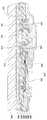
도 1은 종래의 배면발광형 유기전계 발광표시장치의 단면도를 도시한 것이다. 도 1을 참조하면, 절연기판(100)상에 버퍼층(105)이 형성되고, 버퍼층(105)상에 소오스/드레인 영역(111, 115)을 구비하는 반도체층(110)이 형성된다. 게이트 절연막(120)상에 게이트(125)가 형성되며, 층간 절연막(130)상에 콘택홀(131, 135)을 통해 소오스/드레인영역(111, 115)과 각각 연결되는 소오스/드레인 전극(141, 145)이 형성된다. 이로써, TFT 가 제조된다.1 illustrates a cross-sectional view of a conventional bottom emission type organic light emitting display device. Referring to FIG. 1, a
패시베이션막(150)상에 비어홀(155)을 통해 상기 소오스/드레인 전극(141, 145)중 드레인전극(145)에 연결되는 하부전극인 애노드전극(170)이 형성되고, 기판상에 유기박막층(185) 및 상부전극인 캐소드전극(190)이 형성되어 유기EL소자가 제조된다. An
상기한 바와 같은 구조를 갖는 종래의 유기전계 발광표시장치는 콘택홀 또는 비어홀의 테이퍼각이 큰 경우 콘택홀 또는 비어홀 부근 및 애노드전극(170)의 단차진 부분에서 핀홀불량이 발생되거나 또는 애노드전극과 캐소드전극의 단락불량이 발생하였다. 또한, 콘택홀 및 비어홀부근과 애노드전극의 단차진 부분에서 유기발광층이 증착되지 않는 부분이 발생되거나 또는 균일하게 증착되지 않아 다른 부분보다 얇게 증착된다. 그러므로, 애노드전극과 캐소드전극사이에 큰 전압이 인가되면, 유기발광층이 증착되지 않은 부분 또는 얇게 증착된 부분에서 전류밀도가 집중되어 구형의 암점(dark spot)이 발생되었다. 따라서, 암점의 발생에 따라 발광영역이 축소되어 화질이 저하되는 문제점이 있었다.In the conventional organic light emitting display device having the structure as described above, when the taper angle of the contact hole or the via hole is large, a pinhole defect is generated in the vicinity of the contact hole or the via hole and at the stepped portion of the
한편, 기판전면에 증착되는 캐소드전극은 단차진 부분에서는 조밀하게 성막되지 않게 되므로, 캐소드전극의 조밀하게 성막되지 않은 부분을 통해 외부로부터 산소 또는 수분가 용이하게 유입된다. 그러므로, 애노드전극과 캐소드전극간에 높은 전압이 인가되면, 조밀하게 성막되지 않은 부분에서 전류밀도가 집중되어 전자이동현상(electromigration)에 의해 캐소드전극에 공극이 발생되며, 외부산소 유입에 의한 저항증가로 인하여 많은 열이 발생된다. 따라서, 상기 부분에서는 시간이 경과함에 따라 구형의 암점이 발생하게 되는 문제점이 있었다.On the other hand, since the cathode electrode deposited on the front surface of the substrate is not densely formed in the stepped portion, oxygen or moisture is easily introduced from the outside through the densely formed portion of the cathode electrode. Therefore, when a high voltage is applied between the anode electrode and the cathode electrode, the current density is concentrated in the portion not densely formed, so that voids are generated in the cathode electrode by electromigration and increase in resistance due to the inflow of external oxygen. This generates a lot of heat. Therefore, there was a problem in that the spherical dark spots occur with time.
도 4는 종래의 유기전계 발광표시장치에 있어서, 콘택홀 또는 비어홀의 높은 테이퍼각에 의해 발생되는 열화메카니즘을 보여주는 콘택홀부위의 단면사진이다. 도 4를 참조하면, 콘택홀 또는 비어홀부근에서의 핀홀불량에 의해 발생된 캐소드전극의 단락된 부분을 통해 외부로부터 산소 또는 수분이 침투하게 되고, 이에 따라 열화가 확산되는 것을 보여준다.FIG. 4 is a cross-sectional photograph of a contact hole showing a deterioration mechanism caused by a high taper angle of a contact hole or a via hole in a conventional organic light emitting display device. Referring to FIG. 4, it is shown that oxygen or moisture penetrates from the outside through a shorted portion of the cathode electrode caused by a pinhole defect near the contact hole or the via hole, thereby deteriorating the diffusion.
도 5는 유기전계 발광표시장치에 있어서, 콘택홀 또는 비어홀과 같은 홀의 테이퍼각과 불량발생수와의 관계를 나타낸 그래프이다. 도 5를 참조하면, 콘택홀 또는 비어홀의 테이퍼각이 60°이하로 되어야 콘택홀 또는 비어홀부근에서의 불량이 방지됨을 알 수 있다. 도 6은 콘택홀 또는 비어홀의 테이퍼각이 큰 경우, 발광영의 에지부분에서 암점의 발생을 보여주는 사진이다. 도 6을 참조하면, 콘택홀 또는 비어홀에서의 테이퍼각이 75°인 경우 발광영역의 에지부분에서 많은 암점이 발생되었음을 보여준다. 이때, 도면부호 61은 비어홀부근에서 발생된 암점을 나타내고, 62는 콘택홀부근에서 발생된 암점을 나타낸다.5 is a graph showing a relationship between a taper angle of a hole such as a contact hole or a via hole and the number of defective occurrences in an organic light emitting display device. Referring to FIG. 5, it can be seen that a defect in the vicinity of the contact hole or the via hole is prevented when the taper angle of the contact hole or the via hole is 60 ° or less. 6 is a photograph showing the occurrence of dark spots in the edge portion of the light-emitting zero when the taper angle of the contact hole or the via hole is large. Referring to FIG. 6, when the taper angle of the contact hole or the via hole is 75 °, many dark spots are generated at the edge of the emission area. In this case,
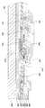
한편, 미국특허 5,684,365에는 애노드전극의 일부분을 노출시키는 개구부의 에지부분에서 패시베이션막의 테이퍼각도를 제한하는 기술이 개시되었다. 도 2는 종래의 배면발광형 유기전계 발광표시장치의 단면도를 도시한 것이다. 도 2를 참조하면, 절연기판(200)상에 버퍼층(205)이 형성되고, 버퍼층(205)상에 소오스/드레인 영역(211, 215)을 구비하는 반도체층(210)이 형성된다. 게이트 절연막(220)상에 게이트(225)가 형성되며, 층간 절연막(230)상에 콘택홀(231, 235)을 통해 소오스/드레인영역(211, 215)과 각각 연결되는 소오스/드레인 전극(241, 245)이 형성된다. 이때, 층간 절연막(230)상에 드레인전극(245)에 연결되는 하부전극인 애노드전극(270)이 형성된다.On the other hand, US Patent 5,684,365 discloses a technique for limiting the taper angle of the passivation film at the edge portion of the opening that exposes a portion of the anode electrode. 2 is a cross-sectional view of a conventional bottom emission type organic light emitting display device. Referring to FIG. 2, a
실리콘 질화막과 같은 절연막으로 된 패시베이션막(250)을 0.5 내지 1.0㎛의 두께로 기판상에 증착한 다음, 패시베이션막(250)을 식각하여 상기 애노드전극(270)의 일부분을 노출시키는 개구부(275)를 형성한다. 이때, 패시베이션막(250)은 개구부(275)의 에지부분에서 애노드전극에 대하여 10 내지 30°의 테이퍼각을 갖도록 형성된다. 기판상에 유기박막층(285) 및 상부전극인 캐소드전극(290)이 형성된다.An
상기한 바와같은 종래의 평판표시장치는 유기발광층의 불량을 방지하기 위하여 화소전극의 일부분을 노출시키기 위한 패시베이션막의 식각시 애노드전극과 접하고 있는 패시베이션막의 테이퍼각을 10 내지 30°로 제한하였다. 그러나, 도 4 및 도 5에 도시된 바와같은 콘택홀 부근, 비어홀부근 및 단차진 부분에서의 핀홀 또는 단락불량이 여전히 발생할 뿐만 아니라 캐소드전극이 조밀하게 성막되지 않아 암점이 발생하는 문제점이 있었다.In the conventional flat panel display as described above, the taper angle of the passivation layer in contact with the anode electrode during etching of the passivation layer for exposing a part of the pixel electrode is limited to 10 to 30 ° in order to prevent defects of the organic light emitting layer. However, pinholes or short-circuit defects in contact holes, via holes, and stepped portions as shown in FIGS. 4 and 5 still occur, and cathode electrodes are not densely formed, resulting in dark spots.
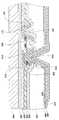
또한, 미국특허 6,246,179에는 비어홀 및 콘택홀 부근 및 단차진 부분에서의 불량을 방지하기 위하여 평탄화기능을 갖는 유기절연층을 사용하는 기술이 개시되었다. 도 3은 종래의 전면발광구조를 갖는 유기전계 발광표시장치의 단면도를 도시한 것이다. 도 3을 참조하면, 절연기판(300)상에 버퍼층(305)이 형성되고, 버퍼층(305)상에 소오스/드레인 영역(311, 315)을 구비하는 반도체층(310)이 형성된다. 게이트 절연막(320)상에 게이트(325)가 형성되며, 층간 절연막(330)상에 콘택홀(331, 335)을 통해 상기 소오스/드레인영역(311, 315)에 각각 연결되는 소오스/드레인 전극(341, 345)이 형성된다.In addition, US Pat. No. 6,246,179 discloses a technique using an organic insulating layer having a planarization function to prevent defects in the vicinity of the via hole and the contact hole and in the stepped portion. 3 is a cross-sectional view of an organic light emitting display device having a conventional top light emitting structure. Referring to FIG. 3, a
패시베이션막(350)상에 평탄화막(360)이 형성되고, 평탄화막(360)상에 비어홀(365)을 통해 상기 소오스/드레인 전극(341, 345)중 하나, 예를 들어 드레인전극(345)에 연결되는 하부전극인 애노드전극(370)이 형성된다. 상기 애노드 전극(370)의 일부분을 노출시키는 개구부(375)를 구비한 화소분리막(380)이 형성되고, 애노드전극(370)과 화소분리막(380)상에 유기박막층(385) 및 상부전극인 캐소드전극(390)이 형성된다.A
상기한 종래의 유기전계 발광표시장치는 유기발광층의 불량을 방지하기 위하여 화소분리막의 테이퍼각을 20 내지 80°로 제한하고, 기판표면의 단차에 의한 콘택홀 또는 비어홀부근에서 발생되는 소자불량을 방지하기 위하여 평탄화막을 사용하였다. 그러나, 화소분리막과 애노드전극사이의 테이퍼각에 따라 소자의 신뢰성이 달라지게 되는데, 테이퍼각도가 높은 경우에는 개구부의 에지부분에서 유기발광층과 캐소드전극이 쉽게 열화되고, 테이퍼각도가 낮은 경우에는, 배선에 의한 단차문제와 기생캐패시터 문제로 화소분리막의 두께와 테이퍼각도를 감소시키는데 한계가 있었다.The conventional organic light emitting display device limits the taper angle of the pixel isolation layer to 20 to 80 ° in order to prevent defects of the organic light emitting layer, and prevents device defects generated near the contact hole or via hole due to the stepped surface of the substrate. In order to achieve this, a planarization film was used. However, the reliability of the device varies depending on the taper angle between the pixel isolation layer and the anode electrode. When the taper angle is high, the organic light emitting layer and the cathode electrode easily deteriorate at the edge portion of the opening, and when the taper angle is low, the wiring Due to the step difference problem and the parasitic capacitor problem, there was a limit in reducing the thickness and taper angle of the pixel isolation layer.
또한, 화소분리막의 사용에 따라 개구율이 더 감소하고, 화소분리막으로부터의 아웃개스(outgas)에 의해 발광영역이 감소하는 픽셀축소현상이 발생하여 수명과 화질이 저하시킬 뿐만 아니라 화소분리막의 증착 및 식각공정이 추가되는 문제점이 있었다.In addition, the aperture ratio is further reduced according to the use of the pixel separation layer, and the pixel reduction phenomenon in which the emission area is reduced due to the outgas from the pixel separation layer occurs, which not only degrades the lifetime and image quality, but also deposits and etches the pixel separation layer. There was a problem that the process is added.
본 발명은 화소전극의 에지부분에서 테이퍼각을 완화시켜 불량을 방지할 수 있는 유기전계 발광표시장치를 제공하는 데 그 목적이 있다.SUMMARY OF THE INVENTION An object of the present invention is to provide an organic light emitting display device which can prevent defects by alleviating a taper angle at an edge portion of a pixel electrode.
본 발명의 다른 목적은 비어홀 및 콘택홀의 테이퍼각을 완화시켜 불량을 방지할 수 있는 유기전계 발광표시장치를 제공하는 데 있다.Another object of the present invention is to provide an organic light emitting display device which can prevent defects by alleviating taper angles of via holes and contact holes.
본 발명의 다른 목적은 개구율을 증대시킬 수 있는 유기전계 발광표시장치를 제공하는 데 있다.Another object of the present invention is to provide an organic light emitting display device capable of increasing the aperture ratio.
본 발명의 또 다른 목적은 수명을 연장시키고 화질을 향상시킬 수 있는 유기전계 발광표시장치를 제공하는 데 있다.Still another object of the present invention is to provide an organic light emitting display device capable of extending the life and improving the image quality.
이와 같은 본 발명의 목적을 달성하기 위하여 본 발명은 절연기판과; 상기 기판상에 형성된 하부 도전층과; 상기 하부 도전층상부에 형성된 상부 도전층과; 상기 상, 하부 도전층사이에 형성되어, 상기 상, 하부 도전층을 연결시켜 주기위한 연결홀을 구비하는 절연막을 구비하며, 상기 연결홀은 60°이하의 테이퍼각을 갖는 평판표시장치를 제공한다.In order to achieve the object of the present invention, the present invention is an insulating substrate; A lower conductive layer formed on the substrate; An upper conductive layer formed on the lower conductive layer; An insulating film is formed between the upper and lower conductive layers, the insulating layer having a connecting hole for connecting the upper and lower conductive layers, and the connecting hole has a taper angle of 60 ° or less. .
바람직하게는 상기 연결홀은 45°이하, 14°이상의 테이퍼각을 갖는다. 상기 평판표시장치는 소오스/드레인영역을 구비하는 반도체층, 게이트전극 및 소오스/드레인전극을 구비하는 박막 트랜지스터를 더 포함하며, 상기 하부 도전층은 상기 소오스/드레인영역이고, 상기 상부 도전층은 소오스/드레인전극이며, 상기 연결홀은 상기 소오스/드레인영역과 상기 소오스/드레인전극을 연결하기 위한 콘택홀이다. 상기 평판표시장치는 적어도 소오스/드레인전극을 구비하는 박막 트랜지스터와, 상기 박막 트랜지스터의 소오스/드레인전극중 하나의 전극에 연결되는 화소전극을 더 포함하며, 상기 하부도전층은 상기 소오스/드레인중 상기 하나의 전극이고, 상기 상부 도전층은 상기 화소전극이며, 상기 연결홀은 상기 하나의 전극과 화소전극을 연결하기 위한 비어홀이다.Preferably, the connection hole has a taper angle of 45 ° or less and 14 ° or more. The flat panel display further includes a semiconductor layer having a source / drain region, a thin film transistor having a gate electrode and a source / drain electrode, wherein the lower conductive layer is the source / drain region, and the upper conductive layer is a source. And a drain electrode, and the connection hole is a contact hole for connecting the source / drain region and the source / drain electrode. The flat panel display further includes a thin film transistor including at least a source / drain electrode, and a pixel electrode connected to one of the source / drain electrodes of the thin film transistor, wherein the lower conductive layer is formed of the source / drain. One electrode, the upper conductive layer is the pixel electrode, and the connection hole is a via hole for connecting the one electrode and the pixel electrode.
또한, 본 발명은 기판상에 형성된 소오스/드레인영역을 구비한 반도체층과; 상기 반도체층 상부에 형성된 게이트와; 상기 반도체층의 소오스/드레인영역에 연결되는 소오스/드레인전극과; 상기 반도체층과 게이트사이의 기판상에 형성된 게이트절연막과; 상기 게이트와 상기 소오스/드레인전극사이의 기판상에 형성된 층간 절연막을 포함하며, 상기 게이트 절연막과 층간 절연막은 상기 소오스/드레인영역과 상기 소오스/드레인전극을 각각 연결시켜 주기위한 소오스/드레인콘택홀을 구비하고, 상기 소오스/드레인 콘택홀은 60°이하의 테이퍼각을 갖는 박막 트랜지스터를 제공한다.In addition, the present invention is a semiconductor layer having a source / drain region formed on a substrate; A gate formed on the semiconductor layer; Source / drain electrodes connected to the source / drain regions of the semiconductor layer; A gate insulating film formed on the substrate between the semiconductor layer and the gate; And an interlayer insulating film formed on the substrate between the gate and the source / drain electrode, wherein the gate insulating film and the interlayer insulating film form a source / drain contact hole for connecting the source / drain region and the source / drain electrode, respectively. The source / drain contact hole includes a thin film transistor having a taper angle of 60 ° or less.
바람직하게는 상기 소오스/드레인 콘택홀은 45°이하의 테이퍼각을 갖는다. 상기 평판표시장치는 상기 소오스/드레인전극과 게이트전극간의 거리가 최소로 되는 위치와 각 콘택홀의 바텀에지간의 거리를 d1 이라하고, 소오스/드레인전극과 게이트전극간의 거리가 최소로 되는 위치에서의 게이트 절연막과 층간 절연막의 두께를 d2 라 할 때, 각 콘택홀의 테이퍼각의 최소값은 θ = tan-1 (d1/d2) 로부터 정해진다.Preferably, the source / drain contact holes have a taper angle of 45 ° or less. In the flat panel display, the distance between the source / drain electrode and the gate electrode is minimized and the distance between the bottom edge of each contact hole is d1, and the gate is positioned at the minimum distance between the source / drain electrode and the gate electrode. When the thickness of the insulating film and the interlayer insulating film is d2, the minimum value of the taper angle of each contact hole is determined from θ = tan-1 (d1 / d2).
또한, 본 발명은 기판상에 형성된 적어도 소오스/드레인전극을 구비한 박막 트랜지스터와; 상기 소오스/드레인전극중 하나의 전극을 노출시키는 개구부를 구비하는 절연막과; 상기 개구부를 통해 상기 하나의 전극에 연결되는 화소전극을 포함하며, 상기 비어홀은 60°이하의 테이퍼각을 가지며, 상기 화소전극은 60°이하의 테이퍼각을 갖는 평판표시장치를 제공한다.The present invention also provides a thin film transistor having at least source and drain electrodes formed on a substrate; An insulating film having an opening that exposes one of the source / drain electrodes; And a pixel electrode connected to the one electrode through the opening, wherein the via hole has a taper angle of 60 ° or less, and the pixel electrode has a taper angle of 60 ° or less.
바람직하게는, 상기 비어홀은 45°이하의 테이퍼각을 가지며, 상기 화소전극은 45°이하의 테이퍼각을 갖는다. 상기 평판표시장치는 상기 화소전극의 두께를 d1이라 하고, 테이퍼각에 따른 화소전극의 상면의 길이와 화소전극의 하면의 길이의 차를 d2라 할 때, 상기 화소전극의 테이퍼각의 최소값은 θ = tan-1 (d1/d2)로부터 정해진다.Preferably, the via hole has a taper angle of 45 ° or less, and the pixel electrode has a taper angle of 45 ° or less. In the flat panel display, when the thickness of the pixel electrode is d1 and the difference between the length of the top surface of the pixel electrode and the length of the bottom surface of the pixel electrode according to the taper angle is d2, the minimum value of the taper angle of the pixel electrode is θ. = tan-1 (d1 / d2).
또한, 본 발명은 절연기판상에 형성된 하부전극과; 상기 하부전극상에 형성된 유기박막층과; 상기 유기박막층상에 형성된 상부전극을 포함하며, 상기 하부전극은 60°이하의 테이퍼각을 가지며, 상기 화소전극의 두께를 d1이라 하고, 테이퍼각에 따른 화소전극의 상면의 길이와 화소전극의 하면의 길이의 차를 d2라 할 때, 상기 화소전극의 테이퍼각의 최소값은 θ = tan-1 (d1/d2) 로부터 정해지는 평판표시장치를 제공한다.In addition, the present invention and the lower electrode formed on the insulating substrate; An organic thin film layer formed on the lower electrode; And an upper electrode formed on the organic thin film layer, wherein the lower electrode has a taper angle of 60 ° or less, the thickness of the pixel electrode is d1, and the length of the top surface of the pixel electrode and the bottom surface of the pixel electrode according to the taper angle. Assuming that the difference between the lengths of ds is d2, the minimum value of the taper angle of the pixel electrode is determined from θ = tan-1 (d1 / d2).
상기 하부전극은 애노드전극과 캐소드전극중 하나의 전극이고, 상기 상부전극은 다른 하나의 전극이다. 상기 하부전극이 투과전극이고, 상부 전극은 반사전극으로서, 상기 유기발광층으로부터 발광된 광은 상기 기판방향으로 방출된다. 상기 하부전극은 반사전극이고, 상부전극은 투과전극으로서, 상기 유기발광층으로부터 발광된 광은 상기 기판과 반대방향으로 방출된다. 상기 하부전극은 투과전극이고, 상기 상부전극은 투과전극으로서, 상기 유기발광층으로부터 발광된 광이 기판방향으로 방출됨과 동시에 기판과 반대방향으로도 방출된다.The lower electrode is one of an anode electrode and a cathode electrode, and the upper electrode is the other electrode. The lower electrode is a transmissive electrode, and the upper electrode is a reflective electrode, and light emitted from the organic light emitting layer is emitted toward the substrate. The lower electrode is a reflective electrode, and the upper electrode is a transmissive electrode, and light emitted from the organic light emitting layer is emitted in a direction opposite to the substrate. The lower electrode is a transmissive electrode, and the upper electrode is a transmissive electrode, and the light emitted from the organic light emitting layer is emitted in a direction toward the substrate and also in a direction opposite to the substrate.
상기 유기발광층은 정공주입층, 정공수송층, 발광층, 정공억제층, 전자수송 층 및 전자주입층으로부터 선택되는 적어도 하나이상의 박막을 포함하고, 상기 발광층은 레이저 열전사법에 의해 형성된 유기박막층, 잉크젯방식에 의해 형성된 유기박막층 및 증착법에 의해 형성된 유기박막층으로부터 선택되는 유기박막층을 포함한다.The organic light emitting layer includes at least one thin film selected from a hole injection layer, a hole transport layer, a light emitting layer, a hole suppression layer, an electron transport layer and an electron injection layer, the light emitting layer is an organic thin film layer formed by laser thermal transfer, inkjet method And an organic thin film layer selected from the organic thin film layer formed by the organic thin film layer formed by the vapor deposition method.
또한, 본 발명은 소오스/드레인영역을 구비한 반도체층과, 상기 소오스/드레인영역의 일부분을 노출시키는 콘택홀을 구비한 제1절연막과, 상기 콘택홀을 통해 상기 소오스/드레인영역에 연결되는 소오스/드레인전극을 구비하는 박막 트랜지스터를 포함하는 절연기판과; 상기 절연기판상에 순차 형성되고, 상기 소오스/드레인 전극중 하나를 노출시키는 비어홀을 구비한 패시베이션을 위한 제2절연막 및 평탄화를 위한 제3절연막과; 상기 제3절연막상에 형성되어 상기 비어홀을 통해 상기 박막 트랜지스터의 하나의 전극에 연결되는 하부전극과; 상기 하부전극상에 형성된 유기박막층과; 상기 유기박막층상에 형성된 상부전극을 포함하며, 상기 비어홀은 60°이하의 테이퍼각을 가지며, 상기 하부전극은 60°이하의 테이퍼각을 갖는 평판표시장치를 제공한다.In addition, the present invention is a semiconductor layer having a source / drain region, a first insulating film having a contact hole for exposing a portion of the source / drain region, and a source connected to the source / drain region through the contact hole An insulating substrate including a thin film transistor having a drain electrode; A second insulating film for passivation and a third insulating film for planarization, which are sequentially formed on the insulating substrate and have via holes for exposing one of the source / drain electrodes; A lower electrode formed on the third insulating layer and connected to one electrode of the thin film transistor through the via hole; An organic thin film layer formed on the lower electrode; An upper electrode is formed on the organic thin film layer. The via hole has a taper angle of 60 ° or less, and the bottom electrode has a taper angle of 60 ° or less.
또한, 본 발명은 소오스/드레인영역을 구비한 반도체층과, 반도체층상에 형성된 게이트와, 상기 반도체층과 게이트사이에 형성된 제1절연막과, 상기 소오스/드레인영역의 일부분을 노출시키는 콘택홀을 구비한 제2절연막과, 상기 콘택홀을 통해 상기 소오스/드레인영역에 연결되는 소오스/드레인전극을 구비하는 박막 트랜지스터를 포함하는 기판과; 상기 기판상에 형성되고, 상기 소오스/드레인 전극중 하나를 노출시키는 비어홀을 구비한 패시베이션을 위한 제3절연막과; 상기 제3절연막상에 형성되어 상기 비어홀을 통해 상기 박막 트랜지스터의 하나의 전극에 연결되는 하부전극과; 상기 하부전극상에 형성된 유기박막층과; 상기 유기박막층상에 형성된 상부전극을 포함하며, 상기 콘택홀는 60°이하의 테이퍼각을 가지며, 상기 비어홀은 60°이하의 테이퍼각을 가지며, 상기 하부전극은 60°이하의 테이퍼각을 갖는 평판표시장치를 제공한다.The present invention also includes a semiconductor layer having a source / drain region, a gate formed on the semiconductor layer, a first insulating film formed between the semiconductor layer and the gate, and a contact hole exposing a portion of the source / drain region. A thin film transistor comprising a second insulating film and a source / drain electrode connected to the source / drain region through the contact hole; A third insulating film formed on the substrate and having a via hole for exposing one of the source / drain electrodes; A lower electrode formed on the third insulating layer and connected to one electrode of the thin film transistor through the via hole; An organic thin film layer formed on the lower electrode; An upper electrode formed on the organic thin film layer, wherein the contact hole has a taper angle of 60 ° or less, the via hole has a taper angle of 60 ° or less, and the bottom electrode has a taper angle of 60 ° or less Provide the device.
또한, 본 발명은 소오스/드레인영역을 구비한 반도체층과, 상기 반도체층상부에 형성된 게이트와, 상기 게이트와 반도체층사이에 형성된 제1절연막과, 상기 소오스/드레인영역의 일부분을 노출시키는 콘택홀을 구비한 제2절연막과, 상기 콘택홀을 통해 상기 소오스/드레인영역에 연결되는 소오스/드레인전극을 구비하는 박막 트랜지스터를 포함하는 기판과; 상기 제2절연막상에 형성되어 상기 소오스/드레인 전극중 하나의 전극에 연결되는 하부전극과; 상기 하부전극의 일부분을 노출시키는 개구부를 구비하는 패시베이션을 위한 제3절연막과; 상기 제3절연막과 하부전극상에 형성되는 유기발광층과; 상기 유기발광층상에 형성된 상부전극을 포함하며, 상기 콘택홀은 60°이하의 테이퍼각을 가지며, 상기 하부전극은 60°이하의 테이퍼각을 갖는 평판표시장치를 제공한다.The present invention also provides a semiconductor layer including a source / drain region, a gate formed on the semiconductor layer, a first insulating layer formed between the gate and the semiconductor layer, and a contact hole exposing a portion of the source / drain region. A substrate including a thin film transistor having a second insulating layer having a second insulating layer and a source / drain electrode connected to the source / drain region through the contact hole; A lower electrode formed on the second insulating layer and connected to one of the source / drain electrodes; A third insulating film for passivation having an opening exposing a portion of the lower electrode; An organic light emitting layer formed on the third insulating layer and the lower electrode; An upper electrode is formed on the organic light emitting layer. The contact hole has a taper angle of 60 ° or less, and the bottom electrode has a taper angle of 60 ° or less.
이하, 본 발명의 실시예를 첨부 도면을 참조하여 설명하면 다음과 같다.Hereinafter, an embodiment of the present invention will be described with reference to the accompanying drawings.
도 7은 본 발명의 제1실시예에 따른 유기전계 발광표시장치의 단면도를 도시한 것이다. 도 7을 참조하면, 절연기판(400)상에 버퍼층(405)이 형성되고, 버퍼층(405)상에 소오스/드레인 영역(411, 415)을 구비하는 반도체층(410)이 형성된다. 게이트 절연막(420)상에 게이트(425)가 형성되며, 층간 절연막(430)상에 콘 택홀(431, 435)을 통해 상기 소오스/드레인영역(411, 415)에 각각 연결되는 소오스/드레인 전극(441, 445)이 형성된다.7 is a cross-sectional view of an organic light emitting display device according to a first embodiment of the present invention. Referring to FIG. 7, a
패시베이션막(450)상에 비어홀(455)을 통해 상기 소오스/드레인 전극(441, 445)중 하나, 예를 들어 드레인전극(445)에 연결되는 하부전극인 애노드전극(470)이 형성된다. 애노드전극(470)을 형성한 다음, 유기박막층(485) 및 캐소드전극(490)을 순차 형성한다. 도면상에는 도시되지 않았으나, 상기 유기박막층(485)은 정공주입층, 정공수송층, R, G 또는 B 발광층, 정공억제층, 전자수송층 및 전자주입층으로부터 선택되는 적어도 하나이상의 박막을 포함한다.An
본 발명의 제1실시예에서는 콘택홀과 비어홀에서의 소자불량을 방지하기 위하여, 상기 콘택홀(431, 435)이 제1테이퍼각(θ41)을 갖도록 상기 층간 절연막(430)과 게이트 절연막(420)을 식각하여 콘택홀(431, 435)을 형성하고, 비어홀(455)이 제2테이퍼각(θ42)을 갖도록 상기 패시베이션막(450)을 식각하여 형성한다.In the first embodiment of the present invention, the
상기 콘택홀(431, 435)의 제1테이퍼각(θ41)은 기판표면에 대하여 콘택홀의 측면이 이루는 각도를 의미하며, 상기 비어홀(455)의 테이퍼각(θ42)은 기판표면에 대하여 비어홀의 측면이 이루는 각도를 의미한다. 상기 콘택홀(431, 435)과 비어홀(455)은 도 5에 도시된 바와같이 불량발생을 방지하기 위해서는 각각 60°이하의 테이퍼각(θ41), (θ42)을 갖는 것이 바람직하다. 더욱 더 바람직하게는, 상기 콘택홀(431, 435)과 비어홀(455)은 45°이하의 테이퍼각을 갖는다.The first taper angle θ41 of the contact holes 431 and 435 means an angle formed by the side of the contact hole with respect to the substrate surface, and the taper angle θ42 of the via
한편, 상기 콘택홀(431), (435)은 상, 하부 도전층, 예를 들어 소오스/드레 인전극(441), (445)과 반도체층(410)에 형성된 소오스/드레인영역(411, 415)을 연결시켜 주기 위한 것으로서, 상기 콘택홀(431), (435)에 형성되는 소오스/드레인전극(441), (445)이 게이트 전극(425)과 인접하게 된다. 그러므로, 게이트전극(425)과 소오스/드레인전극(441), (445)간의 간섭을 최소화하기 위해서는 상기 게이트전극(425)과 소오스/드레인전극(441, 445)은 일정거리를 유지하는 것이 바람직하다. 따라서, 상기 콘택홀(431), (435)의 테이퍼각(θ41)은 일정이상의 각도를 유지하는 것이 바람직하다.The contact holes 431 and 435 may have source and drain
도 8a는 본 발명의 제1실시예에 따른 유기전계발광표시장치에 있어서, 콘택홀의 최소 테이퍼각을 구하는 원리를 설명하기 위한 도면으로서, 콘택홀(431), (435)중 드레인전극(445)과 드레인영역(415)을 연결하기 위한 콘택홀(435)에 한정하여 도시한다.8A is a view for explaining the principle of obtaining the minimum taper angle of a contact hole in the organic light emitting display device according to the first embodiment of the present invention. The
도 8a를 참조하면, 게이트 (425)과 드레인전극(445)간의 최소거리를 d0 라 하고, 게이트 (425)과 드레인전극(445)간의 거리(d0)가 최소로 되는 위치에서 콘택홀의 저면 에지까지의 거리를 d1이라 하며, 게이트(425)와 드레인전극(445)간의 거리가 최소로 되는 위치에서의 절연막의 두께 즉, 층간 절연막(430)의 두께(d22)와 게이트절연막(420)의 두께(d21)의 합을 d2이라 한다. 그러므로, 게이트전극(425)과 드레인전극(455)간의 간섭을 방지하기 위해서는 게이트전극(425)과 드레인전극(455)은 상기 최소거리 d0를 유지해야 하므로, 상기 콘택홀(435)은 상기 게이트전극(425)과 드레인전극(455)간의 최소거리가 유지되는 테이퍼각을 갖는 것이 바람직하다.Referring to FIG. 8A, the minimum distance between the
따라서, 게이트전극(425)과 드레인전극(455)간의 최소거리를 유지하기 위한 콘택홀의 테이퍼각(θ41)은 하기의 식(1)과 같이 주어진다.Therefore, the taper angle θ 41 of the contact hole for maintaining the minimum distance between the
tanθ41 = d2/d1tanθ41 = d2 / d1
θ41 = tan-1 (d2/d1) ..... (1)θ41 = tan-1 (d2 / d1) ..... (1)
고해상도 유기전계 발광표시장치에서, d1은 디자인룰에 따라 2㎛ 이고, 게이트 절연막(420)의 두께(d21)가 0.1㎛, 층간 절연막(430)의 두께(d22)가 0.4㎛인 경우, 상기 식(1)로부터 콘택홀(435)의 테이퍼각(θ41)의 최소값이 구해진다.In the high resolution organic light emitting display device, d1 is 2 μm according to a design rule, the thickness d21 of the
tanθ41 = 0.5㎛/2㎛가 되고, θ41 = tan-1(0.25) = 14° 가 된다.tan θ 41 = 0.5 μm / 2 μm, and θ 41 = tan−1 (0.25) = 14 °.
그러므로, 본 발명의 제1실시예에서, 상기 콘택홀(431), (435)은 60°이하, 14°이상의 테이퍼각(θ41)을 갖는 것이 바람직하다. 또한, 게이트전극과 소오스/드레인전극간의 간섭을 최소화하기 위해서는 게이트(425)도 소정의 제4테이퍼각(θ44)을 갖는 것이 바람직하다. 상기 게이트(425)의 테이퍼각(θ44)은 기판표면에 대하여 게이트 측면이 이루는 각도로서, 상기 콘택홀(431), (435)의 테이퍼각(θ43)과 동일한 것이 바람직하다. 따라서, 상기 게이트(425)의 테이퍼각(θ44)은 바람직하게 60° 이하이고, 더욱 바람직하게는 45° 이하, 14°이상이다. 상기 게이트(425)는 게이트전극물질을 증착한 다음 경사식각방법 등을 이용하여 테이퍼각(θ44)을 갖도록 형성한다.Therefore, in the first embodiment of the present invention, it is preferable that the contact holes 431 and 435 have a taper angle θ41 of 60 ° or less and 14 ° or more. In addition, in order to minimize interference between the gate electrode and the source / drain electrodes, the
한편, 본 발명의 제1실시예에서는 애노드전극의 에지부분에서 발생되는 소자의 불량을 방지하기 위하여 상기 애노드전극(470)이 소정의 제3테이퍼각(θ43)을 갖는 것이 바람직하다. 상기 애노드전극(470)의 테이퍼각(θ43)은 기판표면에 대하여 애노드전극의 측면이 이루는 각도를 의미하는 것으로서, 하부전극인 애노드전극(470)은 애노드전극물질을 증착한 다음 패터닝할 때 제3테이퍼각(θ43)을 갖도록 패터닝한다. 상기 애노드전극(470)은 60° 이하의 테이퍼각(θ43)을 갖는 것이 바람직하며, 45° 이하의 테이퍼각을 갖는 것이 더욱 더 바람직하다.On the other hand, in the first embodiment of the present invention, it is preferable that the
도 8b는 본 발명의 제1실시예에 따른 유기전계발광표시장치에 있어서, 애노드전극의 최소 테이퍼각을 구하는 원리를 설명하기 위한 도면이다.8B is a view for explaining a principle of obtaining a minimum taper angle of an anode electrode in the organic light emitting display device according to the first embodiment of the present invention.
도 8b를 참조하면, 기판(400)상에 형성되는 하부전극인 애노드전극(470)의 두께를 d4 라 하고, 애노드전극(470)이 소정의 제3테이퍼각(θ43)을 가짐에 따라 발생되는 상면의 길이와 하면의 길이와의 편차를 d5 라 할 때, 하부전극의 테이퍼각은 하기의 식(2)와 같이 주어진다.Referring to FIG. 8B, the thickness of the
tanθ43 = d4/d5tanθ43 = d4 / d5
θ43 = tan-1 (d4/d5) ..... (2)θ43 = tan-1 (d4 / d5) ..... (2)
예를 들어, 하부전극의 두께가 0.1㎛이고, 애노드전극(470)의 상면과 하면의 길이 편차가 디자인 룰에 따라 2㎛이하이면, 상기 식(2)로부터 애노드전극(470)의 테이퍼각(θ43)의 최소값이 구해진다.For example, if the thickness of the lower electrode is 0.1 占 퐉 and the length deviation of the top and bottom surfaces of the
tanθ43 = 0.1㎛/2㎛가 되고, θ43 = tan-1(0.05) = 2.9°가 된다.tanθ43 = 0.1 μm / 2 μm, and θ43 = tan−1 (0.05) = 2.9 °.
그러므로, 본 발명의 제1실시예에서, 상기 애노드전극(470)은 60°이하, 2.9°이상의 테이퍼각(θ43)을 갖는 것이 바람직하다.Therefore, in the first embodiment of the present invention, it is preferable that the
본 발명의 제1실시예에서와 같이 콘택홀 및 비어홀의 테이퍼각을 60°이하로 완화시켜 주고, 하부전극의 테이퍼각을 60°이하로 완화시켜 주면, 도 14에 도시된 바와같이 발광영역에서 암점이 발생되지 않음을 보여준다.As in the first embodiment of the present invention, when the taper angles of the contact holes and the via holes are relaxed to 60 ° or less, and the taper angles of the lower electrode are relaxed to 60 ° or less, as shown in FIG. It shows no dark spots.
도 9는 본 발명의 제2실시예에 따른 유기전계 발광표시장치의 단면도를 도시한 것이다. 도 9를 참조하면, 절연기판(500)상에 버퍼층(505)이 형성되고, 버퍼층(505)상에 소오스/드레인 영역(511, 515)을 구비하는 반도체층(510)이 형성된다. 게이트 절연막(520)상에 게이트(525)가 형성되며, 층간 절연막(530)상에 콘택홀(531, 535)을 통해 소오스/드레인영역(541, 545)에 각각 연결되는 소오스/드레인 전극(541, 545)이 형성된다. 상기 층간 절연막(530)상에 상기 소오스/드레인 전극(541, 545)중 하나, 예를 들어 드레인전극(545)에 연결되는 하부전극으로서 애노드전극(570)이 형성된다.9 is a cross-sectional view of an organic light emitting display device according to a second embodiment of the present invention. Referring to FIG. 9, a
상기 콘택홀(531), (535)은 60°이하, 14°이상의 테이퍼각(θ51)을 갖는 것이 바람직하고, 더욱 바람직하게는 45°이하, 14°이상의 테이퍼각(θ51)을 갖는다. 상기 게이트(525)는 상기 콘택홀(531), (535)과 동일한 테이퍼각(θ54)을 가지며, 바람직하게는 60°이하, 14°이상의 테이퍼각(θ54)을 가지며, 더욱 바람직하게는 45°이하, 14°이상의 테이퍼각(θ54)을 갖는다. 상기 애노드전극(570)은 60°이하, 2.9°이상의 테이퍼각(θ53)을 갖는 것이 바람직하다. 더욱 바람직하게는 45°이하, 2.9°이상의 테이퍼각(θ53)을 갖는다.The contact holes 531 and 535 preferably have a taper angle θ51 of 60 ° or less and 14 ° or more, and more preferably have a taper angle θ51 of 45 ° or less and 14 ° or more. The
기판전면에 상기 애노드전극(570)의 일부분을 노출시키는 개구부(575)를 구비하는 패시베이션막(550)이 형성되고, 상기 개구부(575)상의 애노드전극(570)과 패시베이션막(550)상에 유기박막층(585)과 캐소드전극(590)이 형성된다. 상기 패시베이션막(550)에 형성되는 개구부(575)는 40°이하의 테이퍼각(θ53)을 갖는 것이 바람직하다. 도면상에는 도시되지 않았으나, 상기 유기박막층(585)은 정공주입층, 정공수송층, R, G 또는 B 발광층, 정공억제층, 전자수송층 및 전자주입층으로부터 선택되는 적어도 하나이상의 박막을 포함한다.A
도 10은 본 발명의 제3실시예에 따른 유기전계 발광표시장치의 단면도를 도시한 것이다. 도 10을 참조하면, 절연기판(600)상에 버퍼층(605)이 형성되고, 버퍼층(605)상에 소오스/드레인 영역(611, 615)을 구비하는 반도체층(610)이 형성된다. 게이트 절연막(620)상에 게이트(625)가 형성되며, 층간 절연막(630)상에 콘택홀(631, 635)을 통해 상기 소오스/드레인 영역(611, 615)에 각각 연결되는 소오스/드레인 전극(641, 645)이 형성된다.10 is a cross-sectional view of an organic light emitting display device according to a third embodiment of the present invention. Referring to FIG. 10, a
기판전면에 패시베이션막(650)과 평탄화막(660)을 순차 형성하고, 상기 평탄화막(660)과 패시베이션막(650)에 형성된 비어홀(655)을 통해 상기 소오스/드레인 전극(641, 645)중 하나, 예를 들어 드레인전극(645)에 연결되는 애노드전극(670)이 상기 평탄화막(660)상에 형성된다. 애노드전극(670) 및 평탄화막(660)상에 유기박막층(685) 및 캐소드전극(690)이 순차 형성된다. 도면상에는 도시되지 않았으나, 상기 유기박막층(585)은 정공주입층, 정공수송층, R, G 또는 B 발광층, 정공억제층, 전자수송층 및 전자주입층으로부터 선택되는 적어도 하나이상의 박막을 포함한다.The
상기 비어홀(665)은 60°이하, 14°이상의 테이퍼각(θ62)을 갖는 것이 바람 직하고, 더욱 바람직하게는 45°이하, 14°이상의 테이퍼각(θ62)을 갖는다. 상기 애노드전극(670)은 60°이하, 2.9°이상의 테이퍼각(θ63)을 갖는 것이 바람직하다. 더욱 바람직하게는 45°이하, 2.9°이상의 테이퍼각(θ63)을 갖는다.The via hole 665 preferably has a taper angle θ62 of 60 ° or less and 14 ° or more. More preferably, the via hole 665 has a taper angle θ62 of 45 ° or less and 14 ° or more. The
본 발명의 제3실시예의 유기전계 발광표시장치는 박막 트랜지스터를 형성한 다음 애노드전극을 형성하기 전에 평탄화막(660)을 형성하여 기판표면을 평탄화시켜 주므로, 상기 콘택홀(631), (635)을 통상적인 방법으로 형성하거나 또는 본 발명의 제1 및 제2실시예에서와 같이 60°이하, 14°이상의 테이퍼각(θ61)을 갖도록 형성할 수도 있다. 이와 마찬가지로, 상기 게이트전극(625)을 통상적인 방법으로 형성하거나 또는 본 발명의 제1 및 제2실시예에서와 같이 60°이하, 14°이상의 테이퍼각(θ64)을 갖도록 형성할 수도 있다.In the organic light emitting display device according to the third embodiment of the present invention, the
도 11a 및 도 11b는 본 발명의 제3실시예에 따른 유기전계 발광표시장치를 제조하는 제1방법을 설명하기 위한 공정 단면도이다. 도 11a와 같이, 박막 트랜지스터(701)가 형성된 절연기판(700)상에 패시베이션막(750)을 증착하고, 패시베이션막(750)상에 평탄화막(760)을 증착한다. 상기 박막 트랜지스터(701)는 통상적인 방법으로 형성하거나, 제1 및 제2실시예에서와 같이 게이트전극(725)이 소정의 테이퍼각(θ74)을 가지며, 콘택홀(731, 735)이 소정의 테이퍼각(θ71)을 갖도록 형성한다. 상기 패시베이션막(750)은 무기 절연막으로서 질화막을 사용한다. 평탄화막은 유기절연막으로서, BCB 막을 사용한다.11A and 11B are cross-sectional views illustrating a first method of manufacturing an organic light emitting display device according to a third embodiment of the present invention. As shown in FIG. 11A, the
도 11b와 같이, 상기 박막 트랜지스터(701)의 소오스/드레인전극(741), (745)중 드레인전극(745)이 노출되도록 상기 패시베이션막(750)과 평탄화막(760)을 동시에 건식식각하여, 60 °이하, 바람직하게는 40 °이하의 테이퍼각(θ72)을 갖도록 비어홀(755)을 형성한다. 이후, 비어홀(755)을 통해 상기 드레인전극(745)에 연결되는 애노드전극(770)과, 유기박막층(785) 및 캐소드전극(590)을 순차 형성한다.As shown in FIG. 11B, the
도 12a 및 도 12b는 본 발명의 제3실시예에 따른 유기전계 발광표시장치를 제조하는 제2방법을 설명하기 위한 공정 단면도이다. 제2제조방법은 비어홀을 형성하는 방법만이 제1방법과 상이하다. 다시 말하면, 도 12a와 같이, 박막 트랜지스터(801)가 형성된 절연기판(800)상에 질화막과 같은 무기 절연막을 패시베이션막(850)으로 증착하고, 상기 박막 트랜지스터(801)의 소오스/드레인전극(841), (845)중 드레인전극(845)이 노출되도록 상기 패시베이션막(850)을 건식식각하여 1차 비어홀(854)을 형성한다.12A and 12B are cross-sectional views illustrating a second method of manufacturing an organic light emitting display device according to a third embodiment of the present invention. In the second manufacturing method, only the method of forming the via hole is different from the first method. In other words, as shown in FIG. 12A, an inorganic insulating film such as a nitride film is deposited on the insulating
도 12b와 같이, 기판상에 평탄화막(860)으로 BCB 막을 코팅한 다음 상기 1차 비어홀(854)이 노출되도록 평탄화막(860)상에 감광막(853)을 형성한다. 상기 감광막(853)을 마스크로 이용하여 상기 1차 비어홀(854)이 노출되도록 상기 평탄화막(860)을 건식식각하여, 60 °이하, 바람직하게는 40 °이하의 테이퍼각(θ82)을 갖도록 비어홀(855)을 형성한다.As shown in FIG. 12B, the BCB film is coated with the
도 13a 및 도 13b는 본 발명의 제3실시예에 따른 유기전계 발광표시장치를 제조하는 제3방법을 설명하기 위한 공정 단면도이다. 제3제조방법은 광감광성 유기절연막을 사용하여 비어홀을 형성하는 것만이 제2방법과 상이하다. 도 13a와 같이, 박막 트랜지스터(901)가 형성된 절연기판(900)상에 질화막과 같은 무기 절연막을 패시베이션막(960)으로 증착하고, 상기 박막 트랜지스터(901)의 소오스/드레인전극(941), (945)중 드레인전극(945)이 노출되도록 상기 패시베이션막(960)을 건식식각하여 1차 비어홀(954)을 형성한다.13A and 13B are cross-sectional views illustrating a third method of manufacturing an organic light emitting display device according to a third embodiment of the present invention. The third manufacturing method is different from the second method only in forming the via hole using the photosensitive organic insulating film. As shown in FIG. 13A, an inorganic insulating film such as a nitride film is deposited on the insulating
도 13b와 같이, 기판상에 평탄화막(960)으로 광감광성 유기막, 예를 들어 광반응성 BCB 막 또는 포토레지스터를 코팅한 다음 노광공정을 통하여 상기 1차 비어홀(954)이 노출되도록 상기 평탄화막(960)을 식각하여, 60 °이하, 바람직하게는 40 °이하의 테이퍼각을 갖도록 비어홀(955)을 형성한다.As shown in FIG. 13B, a photosensitive organic film, for example, a photoreactive BCB film or a photoresist is coated with a planarization film 960 on a substrate, and then the planarization film is exposed to expose the first via hole 954 through an exposure process. The 960 is etched to form the via
본 발명의 제1 내지 제3실시예에 따른 유기전계 발광표시장치에서는, 하부전극인 애노드전극을 투과전극으로 형성하고 상부전극인 캐소드전극을 반사전극으로 형성하여 배면발광구조, 하부전극인 애노드전극을 반사전극으로 형성하고 캐소드전극을 투과전극으로 형성하여 전면발광구조, 그리고 하부전극인 애노드전극과 상부전극인 캐소드전극을 투과전극으로 형성하여 양면발광구조의 표시장치에 적용가능하다.In the organic light emitting display device according to the first to third embodiments of the present invention, a bottom light emitting structure and a bottom electrode are formed by forming an anode electrode as a lower electrode as a transmissive electrode and a cathode electrode as a reflective electrode. And a cathode electrode as a transmissive electrode to form a front light emitting structure, and an anode electrode as a lower electrode and a cathode electrode as an upper electrode as a transmissive electrode, which is applicable to a display device having a double light emitting structure.
또한, 본 발명의 제1 내지 제3실시예는 애노드전극, 유기박막층 및 캐소드전극이 순차 적층된 통상적인 구조의 유기전계 발광표시장치에 관하여 설명하였으나, 캐소드전극, 유기발광층 및 애노드전극이 순차 형성된 인버티드구조의 유기전계 발광표시장치에도 적용가능하다. 또한, 증착법, 잉크젯방식 또는 레이저 열전사법 등과 같은 다양한 방법을 이용하여 유기발광층을 형성하는 유기전계 발광표시장치에 모두 적용가능하다.In addition, the first to third embodiments of the present invention have been described with respect to an organic light emitting display device having a conventional structure in which an anode electrode, an organic thin film layer, and a cathode electrode are sequentially stacked, but the cathode electrode, the organic light emitting layer, and the anode electrode are sequentially formed. The present invention is also applicable to an organic light emitting display device having an inverted structure. In addition, the organic light emitting display device may be applied to an organic light emitting display device that forms an organic light emitting layer using various methods such as a deposition method, an inkjet method, or a laser thermal transfer method.
이상에서 상세하게 설명한 바와같은 본 발명에 따르면, 비어홀과 콘택홀 그리고 하부전극의 테이터각을 완화시켜 줌으로써, 하부전극의 에지부분 및 콘택홀과 비어홀에서의 불량 및 유기발광층의 불량을 방지할 수 있으므로, 신뢰성 및 수율을 향상시킬 수 있다. According to the present invention as described in detail above, by reducing the data angle of the via hole, the contact hole and the lower electrode, it is possible to prevent defects in the edge portion of the lower electrode, the contact hole and the via hole and the defect of the organic light emitting layer. Can improve the reliability and yield.
또한, 본 발명의 유기박막의 화소분리막을 사용하지 않고도 소자의 불량을 방지할 수 있으므로, 화소분리막의 사용에 따른 불량발생을 방지하고, 공정을 단순화할 수 있는 이점이 있다.In addition, since the defect of the device can be prevented without using the pixel separation film of the organic thin film of the present invention, there is an advantage that can prevent the failure caused by the use of the pixel separation film, and simplify the process.
상기에서는 본 발명의 바람직한 실시예를 참조하여 설명하였지만, 해당 기술 분야의 숙련된 당업자는 하기의 특허 청구의 범위에 기재된 본 발명의 사상 및 영역으로부터 벗어나지 않는 범위 내에서 본 발명을 다양하게 수정 및 변경시킬 수 있음을 이해할 수 있을 것이다.Although described above with reference to a preferred embodiment of the present invention, those skilled in the art will be variously modified and changed within the scope of the invention without departing from the spirit and scope of the invention described in the claims below I can understand that you can.
Claims (37)
Translated fromKoreanPriority Applications (8)
| Application Number | Priority Date | Filing Date | Title |
|---|---|---|---|
| KR1020030084786AKR100611152B1 (en) | 2003-11-27 | 2003-11-27 | Flat Panel Display |
| US10/938,080US7656087B2 (en) | 2003-11-27 | 2004-09-10 | Flat panel display |
| CNB2004100118029ACN100423284C (en) | 2003-11-27 | 2004-09-23 | flat panel display |
| EP04090473AEP1536465B1 (en) | 2003-11-27 | 2004-11-29 | TFT and flat panel display having via holes and anode with tapered edges |
| DE602004021894TDE602004021894D1 (en) | 2003-11-27 | 2004-11-29 | TFT and flat screen with vias and anode contact with beveled side walls |
| AT04090473TATE436090T1 (en) | 2003-11-27 | 2004-11-29 | TFT AND FLAT SCREEN WITH THROUGH CONTACTS AND ANODE CONTACT WITH BEVELED SIDE WALLS |
| JP2004344946AJP4879478B2 (en) | 2003-11-27 | 2004-11-29 | Flat panel display |
| US12/234,554US7936125B2 (en) | 2003-11-27 | 2008-09-19 | Flat panel display |
Applications Claiming Priority (1)
| Application Number | Priority Date | Filing Date | Title |
|---|---|---|---|
| KR1020030084786AKR100611152B1 (en) | 2003-11-27 | 2003-11-27 | Flat Panel Display |
Publications (2)
| Publication Number | Publication Date |
|---|---|
| KR20050051076A KR20050051076A (en) | 2005-06-01 |
| KR100611152B1true KR100611152B1 (en) | 2006-08-09 |
Family
ID=34464755
Family Applications (1)
| Application Number | Title | Priority Date | Filing Date |
|---|---|---|---|
| KR1020030084786AExpired - LifetimeKR100611152B1 (en) | 2003-11-27 | 2003-11-27 | Flat Panel Display |
Country Status (7)
| Country | Link |
|---|---|
| US (2) | US7656087B2 (en) |
| EP (1) | EP1536465B1 (en) |
| JP (1) | JP4879478B2 (en) |
| KR (1) | KR100611152B1 (en) |
| CN (1) | CN100423284C (en) |
| AT (1) | ATE436090T1 (en) |
| DE (1) | DE602004021894D1 (en) |
Cited By (1)
| Publication number | Priority date | Publication date | Assignee | Title |
|---|---|---|---|---|
| US11605687B2 (en) | 2020-07-02 | 2023-03-14 | Samsung Display Co., Ltd. | Pixel and display apparatus including the same |
Families Citing this family (46)
| Publication number | Priority date | Publication date | Assignee | Title |
|---|---|---|---|---|
| JP2002343578A (en)* | 2001-05-10 | 2002-11-29 | Nec Corp | Light-emitting body, light-emitting element, and light-emitting display device |
| KR100552975B1 (en)* | 2003-11-22 | 2006-02-15 | 삼성에스디아이 주식회사 | Active matrix organic light emitting display device and manufacturing method thereof |
| KR100611152B1 (en)* | 2003-11-27 | 2006-08-09 | 삼성에스디아이 주식회사 | Flat Panel Display |
| KR100699996B1 (en)* | 2004-09-02 | 2007-03-26 | 삼성에스디아이 주식회사 | Organic light emitting display device including pad for circuit measurement and manufacturing method |
| JP4757550B2 (en)* | 2005-06-30 | 2011-08-24 | 株式会社 日立ディスプレイズ | Display device and manufacturing method thereof |
| JP2007053355A (en)* | 2005-07-22 | 2007-03-01 | Semiconductor Energy Lab Co Ltd | Semiconductor device |
| WO2007011061A1 (en) | 2005-07-22 | 2007-01-25 | Semiconductor Energy Laboratory Co., Ltd. | Semiconductor device |
| KR100683791B1 (en) | 2005-07-30 | 2007-02-20 | 삼성에스디아이 주식회사 | Thin film transistor substrate and flat panel display device having same |
| KR100731753B1 (en)* | 2005-09-26 | 2007-06-22 | 삼성에스디아이 주식회사 | Both-sides emitting organic electroluminescence display device and fabricating Method of the same |
| KR100782458B1 (en)* | 2006-03-27 | 2007-12-05 | 삼성에스디아이 주식회사 | Organic light emitting display device and manufacturing method |
| KR100805154B1 (en) | 2006-09-15 | 2008-02-21 | 삼성에스디아이 주식회사 | OLED display and manufacturing method thereof |
| TWI364839B (en)* | 2006-11-17 | 2012-05-21 | Au Optronics Corp | Pixel structure of active matrix organic light emitting display and fabrication method thereof |
| JP2008147418A (en)* | 2006-12-11 | 2008-06-26 | Hitachi Ltd | Thin film transistor device, image display device and manufacturing method thereof |
| KR100838082B1 (en) | 2007-03-16 | 2008-06-16 | 삼성에스디아이 주식회사 | OLED display device and manufacturing method |
| WO2008123053A1 (en)* | 2007-03-30 | 2008-10-16 | Toray Industries, Inc. | Positive photosensitive resin composition |
| JP5408856B2 (en)* | 2007-08-30 | 2014-02-05 | キヤノン株式会社 | Organic EL display device |
| KR20100106309A (en)* | 2007-10-15 | 2010-10-01 | 이 아이 듀폰 디 네모아 앤드 캄파니 | Solution processed electronic devices |
| US7635864B2 (en)* | 2007-11-27 | 2009-12-22 | Lg Electronics Inc. | Organic light emitting device |
| KR20100105673A (en) | 2007-12-14 | 2010-09-29 | 이 아이 듀폰 디 네모아 앤드 캄파니 | Backplane structures for electronic devices |
| EP2629590A1 (en)* | 2008-06-17 | 2013-08-21 | Hitachi Ltd. | An organic light-emitting device |
| JP5442234B2 (en)* | 2008-10-24 | 2014-03-12 | 株式会社半導体エネルギー研究所 | Semiconductor device and display device |
| JP5126545B2 (en)* | 2009-02-09 | 2013-01-23 | ソニー株式会社 | Manufacturing method of display device |
| KR101041144B1 (en)* | 2009-08-13 | 2011-06-13 | 삼성모바일디스플레이주식회사 | Thin film transistor, manufacturing method thereof and organic light emitting display device comprising same |
| JP2011113736A (en)* | 2009-11-25 | 2011-06-09 | Toshiba Mobile Display Co Ltd | Organic el device, and method of manufacturing the same |
| KR101394261B1 (en)* | 2010-03-29 | 2014-05-13 | 삼성디스플레이 주식회사 | Organic Light Emitting Device |
| TWI439985B (en)* | 2010-08-26 | 2014-06-01 | Chunghwa Picture Tubes Ltd | Array substrate and manufacturing method thereof |
| KR20120043404A (en) | 2010-10-26 | 2012-05-04 | 삼성모바일디스플레이주식회사 | Display apparatus and method of manufacturing the same |
| KR101839930B1 (en) | 2010-12-29 | 2018-04-27 | 삼성디스플레이 주식회사 | Organic light emitting display apparatus and method of manufacturing organic light emitting display apparatus |
| TWI570809B (en)* | 2011-01-12 | 2017-02-11 | 半導體能源研究所股份有限公司 | Semiconductor device and method of manufacturing same |
| KR102013893B1 (en) | 2012-08-20 | 2019-08-26 | 삼성디스플레이 주식회사 | Flat panel display device and method for fabricating the same |
| JP5418862B2 (en)* | 2012-09-10 | 2014-02-19 | ソニー株式会社 | Display device |
| JP5700870B2 (en)* | 2013-09-27 | 2015-04-15 | 日東電工株式会社 | Organic EL device manufacturing method and organic EL device |
| TWI545733B (en) | 2014-02-11 | 2016-08-11 | 群創光電股份有限公司 | Display panel |
| TWI532154B (en)* | 2014-02-25 | 2016-05-01 | 群創光電股份有限公司 | Display panel and display device |
| CN104659038A (en)* | 2015-03-13 | 2015-05-27 | 京东方科技集团股份有限公司 | Display backboard, method for manufacturing the display backboard, and display device |
| CN105280633B (en)* | 2015-11-30 | 2019-01-01 | 深圳市华星光电技术有限公司 | Tft array substrate and preparation method thereof |
| KR102642198B1 (en)* | 2016-04-04 | 2024-03-05 | 삼성디스플레이 주식회사 | Organic light-emitting display apparatus |
| KR102568781B1 (en)* | 2016-05-31 | 2023-08-22 | 삼성디스플레이 주식회사 | Organic light-emitting display apparatus |
| CN106206672A (en)* | 2016-09-09 | 2016-12-07 | 深圳市华星光电技术有限公司 | AMOLED device and preparation method thereof |
| CN207165572U (en)* | 2017-09-12 | 2018-03-30 | 京东方科技集团股份有限公司 | A kind of array base palte and display device |
| KR102052434B1 (en)* | 2017-12-11 | 2019-12-05 | 엘지디스플레이 주식회사 | Structre for contact and electroluminescent display device using thereof |
| CN108445671A (en)* | 2018-03-16 | 2018-08-24 | 京东方科技集团股份有限公司 | A kind of light path control system and display device |
| CN109904210B (en)* | 2019-03-27 | 2021-08-24 | 合肥鑫晟光电科技有限公司 | Display substrate, manufacturing method thereof and display device |
| CN209729911U (en)* | 2019-06-19 | 2019-12-03 | 京东方科技集团股份有限公司 | A kind of array substrate, display panel and display device |
| CN111244117B (en) | 2020-04-24 | 2020-07-28 | 京东方科技集团股份有限公司 | Array substrate, method for making the same, and display device |
| KR20240025121A (en)* | 2022-08-17 | 2024-02-27 | 삼성디스플레이 주식회사 | Display panel and method of manufacturing the same |
Citations (5)
| Publication number | Priority date | Publication date | Assignee | Title |
|---|---|---|---|---|
| KR950010703A (en)* | 1993-09-23 | 1995-04-28 | 박경팔 | Field emission emitter and method of manufacturing the same |
| KR20010003764A (en)* | 1999-06-25 | 2001-01-15 | 김영환 | Method of manufacturing organic field emission display device |
| JP2002208491A (en)* | 2000-11-09 | 2002-07-26 | Toshiba Corp | Self-luminous display |
| JP2004031262A (en)* | 2002-06-28 | 2004-01-29 | Matsushita Electric Ind Co Ltd | Organic electroluminescence panel |
| KR20040062023A (en)* | 2002-12-31 | 2004-07-07 | 엘지전자 주식회사 | Field emission device and manufacturing method thereof |
Family Cites Families (40)
| Publication number | Priority date | Publication date | Assignee | Title |
|---|---|---|---|---|
| JP2563180B2 (en)* | 1987-07-27 | 1996-12-11 | 日本電信電話株式会社 | Method for manufacturing semiconductor device |
| JPS6433971A (en)* | 1987-07-30 | 1989-02-03 | Asahi Glass Co Ltd | Thin film transistor |
| JPS6430228U (en) | 1987-08-13 | 1989-02-23 | ||
| JPS6433971U (en) | 1987-08-25 | 1989-03-02 | ||
| US5684365A (en)* | 1994-12-14 | 1997-11-04 | Eastman Kodak Company | TFT-el display panel using organic electroluminescent media |
| JPH0955508A (en) | 1995-08-10 | 1997-02-25 | Sanyo Electric Co Ltd | Thin film transistor and manufacturing method thereof |
| US5728608A (en)* | 1995-10-11 | 1998-03-17 | Applied Komatsu Technology, Inc. | Tapered dielectric etch in semiconductor devices |
| TW364275B (en) | 1996-03-12 | 1999-07-11 | Idemitsu Kosan Co | Organic electroluminescent element and organic electroluminescent display device |
| JPH1020331A (en)* | 1996-06-28 | 1998-01-23 | Sharp Corp | Liquid crystal display |
| JP3305961B2 (en) | 1996-09-26 | 2002-07-24 | 株式会社東芝 | Method of manufacturing polycrystalline silicon thin film transistor |
| JPH10148845A (en) | 1996-11-19 | 1998-06-02 | Matsushita Electric Ind Co Ltd | Liquid crystal display device and manufacturing method thereof |
| JP3264364B2 (en) | 1997-01-21 | 2002-03-11 | シャープ株式会社 | Manufacturing method of liquid crystal display device |
| TW477907B (en)* | 1997-03-07 | 2002-03-01 | Toshiba Corp | Array substrate, liquid crystal display device and their manufacturing method |
| TW408351B (en)* | 1997-10-17 | 2000-10-11 | Semiconductor Energy Lab | Semiconductor device and method of manufacturing the same |
| KR100697413B1 (en)* | 1998-07-30 | 2007-03-19 | 마츠시타 덴끼 산교 가부시키가이샤 | Liquid crystal display device, video display device, information processing device, and manufacturing method thereof |
| TW439387B (en)* | 1998-12-01 | 2001-06-07 | Sanyo Electric Co | Display device |
| TW469484B (en) | 1999-03-26 | 2001-12-21 | Semiconductor Energy Lab | A method for manufacturing an electrooptical device |
| JP2001110566A (en) | 1999-10-04 | 2001-04-20 | Sanyo Electric Co Ltd | Manufacturing process for el display apparatus |
| JP2001110575A (en)* | 1999-10-04 | 2001-04-20 | Sanyo Electric Co Ltd | Electroluminescence display device |
| KR100582414B1 (en) | 1999-12-29 | 2006-05-23 | 매그나칩 반도체 유한회사 | Contact hole formation method of semiconductor device |
| JP2001230085A (en)* | 2000-02-17 | 2001-08-24 | Denso Corp | Organic electroluminescent device |
| TW535137B (en)* | 2000-11-09 | 2003-06-01 | Toshiba Corp | Self-illuminating display device |
| CN1174480C (en) | 2000-11-24 | 2004-11-03 | 友达光电股份有限公司 | Method for manufacturing thin film transistor flat display |
| JP2002202737A (en)* | 2000-12-28 | 2002-07-19 | Nec Corp | Manufacturing method of light emitting element, light emitting element |
| JP4939690B2 (en)* | 2001-01-30 | 2012-05-30 | 株式会社半導体エネルギー研究所 | Method for manufacturing semiconductor device |
| KR100571003B1 (en) | 2001-02-06 | 2006-04-13 | 삼성에스디아이 주식회사 | Flat panel display and manufacturing method thereof |
| KR100582724B1 (en) | 2001-03-22 | 2006-05-23 | 삼성에스디아이 주식회사 | Display element for flat panel display apparatus, organic electroluminescent device and method for manufacturing display element for flat panel display using same |
| JP3608613B2 (en)* | 2001-03-28 | 2005-01-12 | 株式会社日立製作所 | Display device |
| KR100796795B1 (en)* | 2001-10-22 | 2008-01-22 | 삼성전자주식회사 | A contact portion of a semiconductor device, a method of manufacturing the same, and a thin film transistor array substrate for a display device including the same, and a method of manufacturing the same |
| CN100380673C (en)* | 2001-11-09 | 2008-04-09 | 株式会社半导体能源研究所 | Light emitting device and manufacturing method thereof |
| US6731064B2 (en)* | 2001-11-20 | 2004-05-04 | International Business Machines Corporation | Yield enchancement pixel structure for active matrix organic light-emitting diode displays |
| KR100845557B1 (en) | 2002-02-20 | 2008-07-10 | 삼성전자주식회사 | Active matrix organic light emitting display device and manufacturing method thereof |
| JP4071652B2 (en)* | 2002-03-04 | 2008-04-02 | 株式会社 日立ディスプレイズ | Organic EL light emitting display |
| JP2003317971A (en)* | 2002-04-26 | 2003-11-07 | Semiconductor Energy Lab Co Ltd | Light emitting device and manufacturing method thereof |
| KR100478759B1 (en)* | 2002-08-20 | 2005-03-24 | 엘지.필립스 엘시디 주식회사 | The organic electro-luminescence device and method for fabricating of the same |
| CN1757052B (en)* | 2003-02-28 | 2010-05-26 | 株式会社半导体能源研究所 | Display device and foldable portable terminal |
| KR100552975B1 (en)* | 2003-11-22 | 2006-02-15 | 삼성에스디아이 주식회사 | Active matrix organic light emitting display device and manufacturing method thereof |
| KR100611152B1 (en)* | 2003-11-27 | 2006-08-09 | 삼성에스디아이 주식회사 | Flat Panel Display |
| KR100611159B1 (en)* | 2003-11-29 | 2006-08-09 | 삼성에스디아이 주식회사 | Organic light emitting display device |
| JP2006058332A (en)* | 2004-08-17 | 2006-03-02 | Seiko Epson Corp | Electro-optical device and electronic apparatus |
- 2003
- 2003-11-27KRKR1020030084786Apatent/KR100611152B1/ennot_activeExpired - Lifetime
- 2004
- 2004-09-10USUS10/938,080patent/US7656087B2/ennot_activeExpired - Lifetime
- 2004-09-23CNCNB2004100118029Apatent/CN100423284C/ennot_activeExpired - Lifetime
- 2004-11-29ATAT04090473Tpatent/ATE436090T1/ennot_activeIP Right Cessation
- 2004-11-29DEDE602004021894Tpatent/DE602004021894D1/ennot_activeExpired - Lifetime
- 2004-11-29JPJP2004344946Apatent/JP4879478B2/ennot_activeExpired - Lifetime
- 2004-11-29EPEP04090473Apatent/EP1536465B1/ennot_activeExpired - Lifetime
- 2008
- 2008-09-19USUS12/234,554patent/US7936125B2/ennot_activeExpired - Lifetime
Patent Citations (5)
| Publication number | Priority date | Publication date | Assignee | Title |
|---|---|---|---|---|
| KR950010703A (en)* | 1993-09-23 | 1995-04-28 | 박경팔 | Field emission emitter and method of manufacturing the same |
| KR20010003764A (en)* | 1999-06-25 | 2001-01-15 | 김영환 | Method of manufacturing organic field emission display device |
| JP2002208491A (en)* | 2000-11-09 | 2002-07-26 | Toshiba Corp | Self-luminous display |
| JP2004031262A (en)* | 2002-06-28 | 2004-01-29 | Matsushita Electric Ind Co Ltd | Organic electroluminescence panel |
| KR20040062023A (en)* | 2002-12-31 | 2004-07-07 | 엘지전자 주식회사 | Field emission device and manufacturing method thereof |
Cited By (2)
| Publication number | Priority date | Publication date | Assignee | Title |
|---|---|---|---|---|
| US11605687B2 (en) | 2020-07-02 | 2023-03-14 | Samsung Display Co., Ltd. | Pixel and display apparatus including the same |
| US12127434B2 (en) | 2020-07-02 | 2024-10-22 | Samsung Display Co., Ltd. | Pixel and display apparatus including the same |
Also Published As
| Publication number | Publication date |
|---|---|
| JP4879478B2 (en) | 2012-02-22 |
| JP2005159368A (en) | 2005-06-16 |
| US20050116630A1 (en) | 2005-06-02 |
| US7936125B2 (en) | 2011-05-03 |
| EP1536465B1 (en) | 2009-07-08 |
| CN100423284C (en) | 2008-10-01 |
| ATE436090T1 (en) | 2009-07-15 |
| US20090072729A1 (en) | 2009-03-19 |
| KR20050051076A (en) | 2005-06-01 |
| DE602004021894D1 (en) | 2009-08-20 |
| CN1622361A (en) | 2005-06-01 |
| US7656087B2 (en) | 2010-02-02 |
| EP1536465A1 (en) | 2005-06-01 |
Similar Documents
| Publication | Publication Date | Title |
|---|---|---|
| KR100611152B1 (en) | Flat Panel Display | |
| KR100496425B1 (en) | OLED and fabrication method thereof | |
| US7839077B2 (en) | Organic light emitting display and method of fabricating the same | |
| CN101271919B (en) | Display substrate, organic light emitting diode display device and manufacturing method thereof | |
| US7888856B2 (en) | Organic electroluminescence device and display apparatus containing the same, method for making organic electroluminescence device and method for making display apparatus | |
| US12402516B2 (en) | Display panel with CVD encapsulation layers, display apparatus comprising the encapsulation layers, and method for manufacturing the display panel | |
| JP4113197B2 (en) | Organic electroluminescence display | |
| WO2019186806A1 (en) | Organic el display device and manufacturing method for organic el display device | |
| US12004380B2 (en) | Organic light-emitting diode display device and manufacturing method thereof | |
| CN102983281B (en) | Organic light emitting apparatus and manufacture method thereof | |
| KR100852252B1 (en) | Display Device and Manufacturing Method Thereof | |
| US20230255063A1 (en) | Display device and manufacturing method thereof | |
| US7592624B2 (en) | Organic light emitting display including a protruding insulating layer and method of fabricating the same | |
| KR100712212B1 (en) | Manufacturing method of organic light emitting device | |
| US20240365600A1 (en) | Display device and manufacturing method of display device | |
| JP2006261058A (en) | Organic el element, display device, and manufacturing method of organic el element | |
| US20240389400A1 (en) | Display device and manufacturing method of display device | |
| US20250275377A1 (en) | Mother substrate for display device and manufacturing method of display device | |
| US20230269991A1 (en) | Display device | |
| US20250048847A1 (en) | Display device and manufacturing method thereof | |
| US20240196693A1 (en) | Display device and mother substrate for display device | |
| US20230309350A1 (en) | Display device and manufacturing method of the same | |
| KR102179972B1 (en) | Manufacturing method of metal line and thin transistor array panel, and organic light emitting diode display | |
| KR100807552B1 (en) | Organic light emitting display device and manufacturing method thereof |
Legal Events
| Date | Code | Title | Description |
|---|---|---|---|
| A201 | Request for examination | ||
| PA0109 | Patent application | Patent event code:PA01091R01D Comment text:Patent Application Patent event date:20031127 | |
| PA0201 | Request for examination | ||
| PG1501 | Laying open of application | ||
| E902 | Notification of reason for refusal | ||
| PE0902 | Notice of grounds for rejection | Comment text:Notification of reason for refusal Patent event date:20051007 Patent event code:PE09021S01D | |
| E90F | Notification of reason for final refusal | ||
| PE0902 | Notice of grounds for rejection | Comment text:Final Notice of Reason for Refusal Patent event date:20060215 Patent event code:PE09021S02D | |
| E701 | Decision to grant or registration of patent right | ||
| PE0701 | Decision of registration | Patent event code:PE07011S01D Comment text:Decision to Grant Registration Patent event date:20060713 | |
| GRNT | Written decision to grant | ||
| PR0701 | Registration of establishment | Comment text:Registration of Establishment Patent event date:20060803 Patent event code:PR07011E01D | |
| PR1002 | Payment of registration fee | Payment date:20060804 End annual number:3 Start annual number:1 | |
| PG1601 | Publication of registration | ||
| PR1001 | Payment of annual fee | Payment date:20090728 Start annual number:4 End annual number:4 | |
| PR1001 | Payment of annual fee | Payment date:20100727 Start annual number:5 End annual number:5 | |
| PR1001 | Payment of annual fee | Payment date:20110729 Start annual number:6 End annual number:6 | |
| FPAY | Annual fee payment | Payment date:20120730 Year of fee payment:7 | |
| PR1001 | Payment of annual fee | Payment date:20120730 Start annual number:7 End annual number:7 | |
| FPAY | Annual fee payment | Payment date:20130731 Year of fee payment:8 | |
| PR1001 | Payment of annual fee | Payment date:20130731 Start annual number:8 End annual number:8 | |
| FPAY | Annual fee payment | Payment date:20160801 Year of fee payment:11 | |
| PR1001 | Payment of annual fee | Payment date:20160801 Start annual number:11 End annual number:11 | |
| FPAY | Annual fee payment | Payment date:20180802 Year of fee payment:13 | |
| PR1001 | Payment of annual fee | Payment date:20180802 Start annual number:13 End annual number:13 | |
| FPAY | Annual fee payment | Payment date:20190801 Year of fee payment:14 | |
| PR1001 | Payment of annual fee | Payment date:20190801 Start annual number:14 End annual number:14 | |
| PR1001 | Payment of annual fee | Payment date:20200803 Start annual number:15 End annual number:15 | |
| PR1001 | Payment of annual fee | Payment date:20210802 Start annual number:16 End annual number:16 | |
| PR1001 | Payment of annual fee | Payment date:20230801 Start annual number:18 End annual number:18 | |
| PC1801 | Expiration of term | Termination date:20240527 Termination category:Expiration of duration |