KR100611040B1 - Laser heat treatment device - Google Patents
Laser heat treatment deviceDownload PDFInfo
- Publication number
- KR100611040B1 KR100611040B1KR1020010086423AKR20010086423AKR100611040B1KR 100611040 B1KR100611040 B1KR 100611040B1KR 1020010086423 AKR1020010086423 AKR 1020010086423AKR 20010086423 AKR20010086423 AKR 20010086423AKR 100611040 B1KR100611040 B1KR 100611040B1
- Authority
- KR
- South Korea
- Prior art keywords
- laser beam
- laser
- substrate
- thin film
- heat treatment
- Prior art date
- Legal status (The legal status is an assumption and is not a legal conclusion. Google has not performed a legal analysis and makes no representation as to the accuracy of the status listed.)
- Expired - Fee Related
Links
Images


Classifications
- G—PHYSICS
- G02—OPTICS
- G02F—OPTICAL DEVICES OR ARRANGEMENTS FOR THE CONTROL OF LIGHT BY MODIFICATION OF THE OPTICAL PROPERTIES OF THE MEDIA OF THE ELEMENTS INVOLVED THEREIN; NON-LINEAR OPTICS; FREQUENCY-CHANGING OF LIGHT; OPTICAL LOGIC ELEMENTS; OPTICAL ANALOGUE/DIGITAL CONVERTERS
- G02F1/00—Devices or arrangements for the control of the intensity, colour, phase, polarisation or direction of light arriving from an independent light source, e.g. switching, gating or modulating; Non-linear optics
- G02F1/01—Devices or arrangements for the control of the intensity, colour, phase, polarisation or direction of light arriving from an independent light source, e.g. switching, gating or modulating; Non-linear optics for the control of the intensity, phase, polarisation or colour
- G02F1/13—Devices or arrangements for the control of the intensity, colour, phase, polarisation or direction of light arriving from an independent light source, e.g. switching, gating or modulating; Non-linear optics for the control of the intensity, phase, polarisation or colour based on liquid crystals, e.g. single liquid crystal display cells
- G02F1/133—Constructional arrangements; Operation of liquid crystal cells; Circuit arrangements
- G02F1/136—Liquid crystal cells structurally associated with a semi-conducting layer or substrate, e.g. cells forming part of an integrated circuit
- H—ELECTRICITY
- H01—ELECTRIC ELEMENTS
- H01L—SEMICONDUCTOR DEVICES NOT COVERED BY CLASS H10
- H01L21/00—Processes or apparatus adapted for the manufacture or treatment of semiconductor or solid state devices or of parts thereof
- H01L21/02—Manufacture or treatment of semiconductor devices or of parts thereof
- H01L21/04—Manufacture or treatment of semiconductor devices or of parts thereof the devices having potential barriers, e.g. a PN junction, depletion layer or carrier concentration layer
- H01L21/18—Manufacture or treatment of semiconductor devices or of parts thereof the devices having potential barriers, e.g. a PN junction, depletion layer or carrier concentration layer the devices having semiconductor bodies comprising elements of Group IV of the Periodic Table or AIIIBV compounds with or without impurities, e.g. doping materials
- H01L21/30—Treatment of semiconductor bodies using processes or apparatus not provided for in groups H01L21/20 - H01L21/26
- H01L21/324—Thermal treatment for modifying the properties of semiconductor bodies, e.g. annealing, sintering
- H—ELECTRICITY
- H01—ELECTRIC ELEMENTS
- H01L—SEMICONDUCTOR DEVICES NOT COVERED BY CLASS H10
- H01L21/00—Processes or apparatus adapted for the manufacture or treatment of semiconductor or solid state devices or of parts thereof
- H01L21/67—Apparatus specially adapted for handling semiconductor or electric solid state devices during manufacture or treatment thereof; Apparatus specially adapted for handling wafers during manufacture or treatment of semiconductor or electric solid state devices or components ; Apparatus not specifically provided for elsewhere
- H01L21/67005—Apparatus not specifically provided for elsewhere
- H01L21/67011—Apparatus for manufacture or treatment
- H01L21/67098—Apparatus for thermal treatment
- G—PHYSICS
- G02—OPTICS
- G02F—OPTICAL DEVICES OR ARRANGEMENTS FOR THE CONTROL OF LIGHT BY MODIFICATION OF THE OPTICAL PROPERTIES OF THE MEDIA OF THE ELEMENTS INVOLVED THEREIN; NON-LINEAR OPTICS; FREQUENCY-CHANGING OF LIGHT; OPTICAL LOGIC ELEMENTS; OPTICAL ANALOGUE/DIGITAL CONVERTERS
- G02F1/00—Devices or arrangements for the control of the intensity, colour, phase, polarisation or direction of light arriving from an independent light source, e.g. switching, gating or modulating; Non-linear optics
- G02F1/01—Devices or arrangements for the control of the intensity, colour, phase, polarisation or direction of light arriving from an independent light source, e.g. switching, gating or modulating; Non-linear optics for the control of the intensity, phase, polarisation or colour
- G02F1/13—Devices or arrangements for the control of the intensity, colour, phase, polarisation or direction of light arriving from an independent light source, e.g. switching, gating or modulating; Non-linear optics for the control of the intensity, phase, polarisation or colour based on liquid crystals, e.g. single liquid crystal display cells
- G02F1/133—Constructional arrangements; Operation of liquid crystal cells; Circuit arrangements
- G02F1/136—Liquid crystal cells structurally associated with a semi-conducting layer or substrate, e.g. cells forming part of an integrated circuit
- G02F1/1362—Active matrix addressed cells
- G02F1/136277—Active matrix addressed cells formed on a semiconductor substrate, e.g. of silicon
- G02F1/136281—Active matrix addressed cells formed on a semiconductor substrate, e.g. of silicon having a transmissive semiconductor substrate
Landscapes
- Physics & Mathematics (AREA)
- Engineering & Computer Science (AREA)
- General Physics & Mathematics (AREA)
- Microelectronics & Electronic Packaging (AREA)
- Condensed Matter Physics & Semiconductors (AREA)
- Nonlinear Science (AREA)
- Manufacturing & Machinery (AREA)
- Computer Hardware Design (AREA)
- Power Engineering (AREA)
- Crystallography & Structural Chemistry (AREA)
- Chemical & Material Sciences (AREA)
- Optics & Photonics (AREA)
- Mathematical Physics (AREA)
- Recrystallisation Techniques (AREA)
Abstract
Translated fromKoreanDescription
Translated fromKorean도 1은 레이저 에너지 밀도별 실리콘의 결정화 곡선 그래프를 나타낸 도면.1 is a graph showing a crystallization curve graph of silicon by laser energy density.
도 2는 종래의 레이저 결정화 장치를 이용한 SLS 결정화 전체 공정도를 나타낸 도면.2 is a view showing an overall process of SLS crystallization using a conventional laser crystallization apparatus.
도 3a, 3b는 상기 도 2의 SLS 결정화 장치를 이용한 실리콘의 결정화 단계를 각각 나타낸 도면.3A and 3B are diagrams illustrating crystallization steps of silicon using the SLS crystallization apparatus of FIG. 2, respectively.
도 4는 기판 온도에 따른 실리콘의 측면 성장 길이 그래프를 나타낸 도면.4 shows a graph of lateral growth length of silicon with substrate temperature.
도 5는 본 발명에 따른 레이저 결정화 장치를 이용한 SLS 결정화 전체 공정도를 나타낸 도면.5 is a view showing an overall process of SLS crystallization using a laser crystallization apparatus according to the present invention.
< 도면의 주요 부분에 대한 부호의 설명 ><Description of Symbols for Main Parts of Drawings>
100 : 절연기판 102 : 비정질 실리콘 박막100: insulating substrate 102: amorphous silicon thin film
104 : 기판104: Substrate
112a : 펄스 레이저 빔(pulse laser beam)112a: pulse laser beam
112b : CW 레이저 빔(continuous wave laser beam)112b: CW laser beam
112 : 레이저 빔112: laser beam
114a : 제 1 레이저 발생장치 114b : 제 2 레이저 발생장치114a: first laser generator 114b: second laser generator
114 : 레이저 발생장치 116 : 호모제나이저(homogenizer)114: laser generator 116: homogenizer
118 : 슬릿 마스크(slit mask) 120 : 프로젝션 렌즈(projection lens)118
122 : 미러(mirror)122: mirror
134 : 프리시젼 스테이지(precision stage)134: Precision stage
136 : 패스홀(path hole)136: path hole
본 발명은 결정질 실리콘 박막의 제조방법에 관한 것으로, 특히, 레이저를 이용한 결정질 실리콘 박막의 제조방법에 관한 것이다.The present invention relates to a method for manufacturing a crystalline silicon thin film, and more particularly, to a method for manufacturing a crystalline silicon thin film using a laser.
최근에 액정표시장치는 소비전력이 낮고, 휴대성이 양호한 기술집약적이며 부가가치가 높은 차세대 첨단 디스플레이(display)소자로 각광받고 있다.Recently, liquid crystal displays have been spotlighted as next generation advanced display devices having low power consumption, good portability, technology-intensive, and high added value.
상기 액정표시장치는 박막트랜지스터(Thin Film Transistor ; TFT)를 포함하는 어레이 기판과 컬러 필터(color filter) 기판 사이에 액정을 주입하여, 이 액정의 이방성에 따른 빛의 굴절률 차이를 이용해 영상효과를 얻는 비발광 소자에 의한 화상표시장치를 뜻한다.The liquid crystal display device injects a liquid crystal between an array substrate including a thin film transistor (TFT) and a color filter substrate to obtain an image effect by using a difference in refractive index of light according to the anisotropy of the liquid crystal. Means an image display device by a non-light emitting element.
현재의 평판 디스플레이 분야에서는 능동구동 액정표시 소자(AMLCD : Active Matrix Liquid Crystal Display)가 주류를 이루고 있다. AMLCD에서는 박막 트랜지스터(TFT : Thin Film Transistor) 하나가 화소 한 개의 액정에 걸리는 전압을 조절하여 화소의 투과도를 변화시키는 스위칭 소자로 사용된다.In the current flat panel display field, active matrix liquid crystal display (AMLCD) is the mainstream. In an AMLCD, a thin film transistor (TFT) is used as a switching element to change the transmittance of a pixel by adjusting a voltage applied to a liquid crystal of one pixel.
이러한 박막트랜지스터 반도체 소자로는 전계효과 이동도가 높으며, 광전류가 적어 구동회로부 일체형 액정표시장치나 빛이 많이 쬐이는 디스플레이 용도로 다결정 실리콘이 주로 이용된다.Such thin film transistor semiconductor devices have high field effect mobility and low photocurrent, so that polycrystalline silicon is mainly used for a liquid crystal display device integrated with a driving circuit unit or a display with a lot of light.
이 다결정 실리콘의 제조방법은 공정온도에 따라 저온 공정과 고온 공정으로 나눌 수 있으며, 이중 고온 공정은 공정온도가 1000℃ 근처로 절연기판의 변형온도 이상의 온도조건이 요구되어 열저항력이 높은 고가의 석영기판을 써야 된다는 점과, 이 고온 공정에 의한 다결정 실리콘 박막의 경우 성막시 높은 표면조도(surface roughness)와 미세 결정립 등의 저품위 결정성으로, 저온공정에 의한 다결정 실리콘보다 소자응용 특성이 떨어진다는 단점이 있으므로, 저온 증착이 가능한 비정질 실리콘을 이용하여 이를 결정화시켜 다결정 실리콘으로 형성하는 기술이 연구/개발되고 있다.This method of manufacturing polycrystalline silicon can be divided into low temperature process and high temperature process according to the process temperature, and the high temperature process is expensive quartz with high heat resistance because process temperature is higher than 1000 ℃ and temperature condition above the deformation temperature of insulation board is required. It is necessary to use a substrate, and low temperature crystallinity such as high surface roughness and fine grains during film formation in the case of polycrystalline silicon thin film by high temperature process, and device application characteristics are lower than polycrystalline silicon due to low temperature process. As a result, a technology for forming a polycrystalline silicon by crystallizing it using amorphous silicon capable of low temperature deposition has been researched and developed.
상기 저온 공정은 레이저 열처리(laser annealing), 금속유도 결정화(Metal Induced Crystallization) 등으로 분류할 수 있다.The low temperature process may be classified into laser annealing, metal induced crystallization, and the like.
이중 레이저 열처리 공정은 펄스(pulse)형태의 레이저 빔을 기판 상에 조사하는 방법을 이용하는데, 이 펄스형태의 레이저 빔에 의하면 용융과 응고가 10 ~ 102 나노세컨드(nano second) 단위로 반복되어 진행되는 방식으로써, 하부 절연기판 에 가해지는 데미지(damage)를 최소화시킬 수 있는 장점을 가져 저온 결정화 공정에서 가장 주목받고 있다.The dual laser heat treatment process uses a method of irradiating a pulsed laser beam onto a substrate, and according to the pulsed laser beam, melting and solidification are repeated in units of 10 to 102 nanoseconds. As a method of progressing, it has the advantage of minimizing the damage (damage) to the lower insulating substrate has attracted the most attention in the low temperature crystallization process.
이하, 도면을 참조하여 레이저 열처리 공정에 따른 실리콘의 결정화 공정에 대해서 설명한다.Hereinafter, a crystallization process of silicon according to a laser heat treatment process will be described with reference to the drawings.
도 1은 레이저 에너지 밀도별 실리콘의 결정화 곡선 그래프를 나타낸 도면으로서, 결정립의 크기에 따라 레이저 결정화 영역을 분류하였다.FIG. 1 is a graph illustrating crystallization curves of silicon according to laser energy densities, and classified laser crystallization regions according to grain sizes.
도시한 바와 같이, 그래프상의 제 1 영역은 부분 용융 영역(partial melting regime)으로서, 실리콘층의 표면만을 용융시켜 작은 결정립(G)을 형성하게 된다.As shown, the first region on the graph is a partial melting regime, in which only the surface of the silicon layer is melted to form small crystal grains (G).
제 2 영역은 완전 용융 근접 영역(near-complete melting regime)으로서, 측면 성장에 의해, 제 1 영역보다 조대한 결정립을 형성할 수 있으나, 균일한 결정립을 수득하기는 어렵다.The second region is a near-complete melting regime, which can form coarse grains than the first region by lateral growth, but it is difficult to obtain uniform grains.
제 3 영역은 완전 용융 영역(complete melting regime)으로서, 비정질 실리콘층 전체를 용융시킨 후 균일한 결정핵 생성(homogeneous nucleation)에 의해 미세한(fine) 결정립으로 형성된다.The third region is a complete melting regime, and after melting the entire amorphous silicon layer, the third region is formed into fine grains by homogeneous nucleation.
즉, 레이저 열처리 공정을 이용하여 다결정 실리콘을 제조하는 공정에서는 제 2 영역대의 에너지 밀도를 이용하여 균일하게 조대한 결정립을 형성하기 위하여, 레이저 빔의 조사횟수 및 중첩비를 조절한다.That is, in the process of manufacturing polycrystalline silicon using the laser heat treatment process, the number of irradiation times and the overlap ratio of the laser beam are controlled to form coarse crystal grains uniformly using the energy density of the second region.
그러나, 다결정 실리콘의 다수 개의 결정립계는 전류흐름의 장애요소로 작용하여 신뢰성있는 박막트랜지스터 소자를 제공하기 어렵고, 다수 개의 결정립내에서는 전자간의 충돌에 의한 충돌전류 및 열화에 의해 절연막이 파괴되어 제품불량을 초래하는 문제점을 가지고 있으므로, 이러한 문제점을 개선하기 위하여, 실리콘 결정립이 액상 실리콘과 고상 실리콘의 경계면에서, 그 경계면에 대하여 수직 방향으로 성장한다는 사실을 이용한 SLS 결정화 기술에 의해 단결정 실리콘을 형성하는 기술(Robert S. Sposilli, M. A. Crowder, and James S. Im, Mat. Res. Soc. Symp. Proc. Vol. 452, 956~957, 1997)이 제안되었다.However, a large number of grain boundaries of polycrystalline silicon act as a barrier to current flow, making it difficult to provide a reliable thin film transistor element.In a plurality of grains, an insulating film is destroyed due to collision current and deterioration due to collision between electrons, thereby preventing product defects. In order to solve this problem, a technique for forming single crystal silicon by the SLS crystallization technique using the fact that the silicon grains grow at the interface between the liquid silicon and the solid silicon in a direction perpendicular to the interface ( Robert S. Sposilli, MA Crowder, and James S. Im, Mat. Res. Soc. Symp. Proc. Vol. 452, 956-957, 1997).
상기 SLS 결정화 기술에서는, 레이저 에너지 크기와 레이저 빔의 조사범위 및 그 이동거리(translation distance)를 적절히 조절하여, 실리콘 결정립을 소정의 길이만큼 측면성장시킴으로써, 비정질 실리콘을 단결정 수준으로 결정화시킬 수 있다.In the SLS crystallization technique, the amorphous silicon can be crystallized to a single crystal level by appropriately adjusting the laser energy size, the irradiation range of the laser beam, and the translation distance thereof, and laterally growing the silicon grains by a predetermined length.
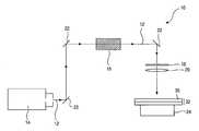
도 2는 종래의 레이저 결정화 장치를 이용한 SLS 결정화 전체 공정도를 나타낸 도면이고, 도 3a, 3b는 상기 도 2의 SLS 결정화 장치를 이용한 실리콘의 결정화 단계를 각각 나타낸 도면이다.2 is a view showing the overall process of SLS crystallization using a conventional laser crystallization device, Figures 3a, 3b is a view showing the crystallization step of silicon using the SLS crystallization device of FIG.
도 2에서, 상기 레이저 결정화 장치(10)는 펄스 형태의 레이저 빔(12)을 발생시키는 레이저 발생장치(14)와, 레이저 빔(12)을 원하는 형상으로의 에너지 밀도를 조절하는 호모제나이저(16 ; homogenizer)와, 호모제나이저(16)를 통해 원하는 에너지 밀도로 조절된 레이저 빔(12)을 비정질 실리콘 박막(30)이 형성된 기판(32)에 나누어 조사시키는 슬릿 마스크(18)와, 슬릿 마스크(18) 하부에 위치하여 레이저 빔(12)의 포커싱(focusing)을 통해 에너지 밀도를 높이는 프로젝션 렌즈(20 ; projection lens)로 구성되며, 레이저 빔(12)의 진행방향을 조정하는 다수 개의 미러(22)가 구비되어 있다.In FIG. 2, the
그리고, 상기 프로젝션 렌즈(20)와 대향되게 기판(30)을 X-Y 방향으로 일정하게 이동시키는 프리시젼 스테이지(24 ; precision stage)가 배치되어 있다.A
이때, 상기 비정질 실리콘 박막(30)을 레이저 결정화하기 위해서는 레이저 빔(12)을 가늘고 길게 만들어야 하며 기판(32)을 정밀하게 이동시켜야 한다.At this time, in order to laser crystallize the amorphous silicon
도 3a는 제 1 레이저 샷에 의한 실리콘의 결정화 조직 상태를 나타낸 도면으로서, 상기 비정질 실리콘 박막(30) 상에 레이저 빔(12)을 슬릿 마스크(18)를 통해 일정 슬릿 폭(I)으로 조사시키면, 실리콘의 결정성장은 조사된 영역의 가장자리로부터 안쪽으로 성장하는 측면 응고(lateral solidification)에 의해 일어난다. 이때 측면 방향으로 성장하는 실리콘 결정(34)의 길이를 레이저 빔(12)의 에너지와 실리콘 박막의 두께, 기판(32) 온도에 따라 달라진다.3A is a view showing a crystallization structure state of silicon by a first laser shot. When the
도 3b는 제 n 레이저 샷을 조사하면서 조사영역을 이동했을 때 실리콘의 결정화 조직 상태를 나타낸 도면으로서, 레이저 빔(12)을 슬릿 마스크(18)를 통해 비정질 실리콘 박막(30) 상에 조사할 때 첫번째 조사된 영역을 일정부분 중첩시키면서 다음 조사를 행하면 첫번째 조사 단계에서 형성된 실리콘 결정(34)들이 씨드(seed)가 되어 다음 조사 단계에서 실리콘 결정들이 측면방향으로 연속적으로 길게 성장시킬 수 있다. 이때, 중첩되는 정도는 첫번째 조사시 형성된 실리콘 결정(34)의 측면방향 길이에 좌우된다.3B is a view showing the crystallization structure state of silicon when the irradiation area is moved while irradiating the nth laser shot, and when the
본 발명에서는, 단결정 실리콘 박막 제작을 위한 레이저를 이용한 SLS 결정 화 공정 효율을 향상시키는 것을 목적으로 한다.In the present invention, it is an object to improve the SLS crystallization process efficiency using a laser for producing a single crystal silicon thin film.
이를 위하여, 본 발명에서는 SLS 결정화 특성을 향상시키기 위해 기판을 예열시킬 수 있는 별도의 레이저 장치를 구비하도록 한다.To this end, the present invention is to provide a separate laser device that can preheat the substrate to improve the SLS crystallization characteristics.
도 4는 기판 온도에 따른 실리콘의 측면 성장 길이 그래프를 나타낸 도면이다.4 is a graph showing lateral growth length of silicon according to substrate temperature.
도시한 바와 같이, 기판 온도가 높아질 수록 실리콘의 측면 성장 길이가 비례적으로 길어지기 때문에, SLS 결정화 공정 효율을 높이기 위해 기판온도를 높일 수 있는 장치를 구비하게 되면 실리콘의 결정화 특성을 향상시킬 수 있다.
As shown, since the lateral growth length of the silicon increases proportionally as the substrate temperature increases, the crystallization characteristics of the silicon can be improved by providing a device capable of increasing the substrate temperature in order to increase the efficiency of the SLS crystallization process. .
상기 목적을 달성하기 위하여, 본 발명에서는 순차 측면 고상(sequential lateral solidification) 결정화 기술에 의해 단결정 실리콘 박막을 제조하기 위한 레이저 열처리 장치에 있어서, 비정질 실리콘(a-Si) 박막이 형성된 기판과; 상기 비정질 실리콘 박막 상에 펄스 레이저 빔(pulse laser beam)을 조사하는 제 1 레이저 장치와; 상기 기판을 일정하게 이동시키며, 상기 펄스 레이저 빔폭과 대응되는 패스홀(path hole)을 가지는 프리시젼 스테이지(precision stage)와; 상기 프리시젼 스테이지의 패스홀을 통해 기판의 하부쪽으로 CW(continuous wave) 레이저 빔을 조사하는 제 2 레이저 장치를 포함하는 레이저 열처리 장치를 제공한다.In order to achieve the above object, the present invention provides a laser heat treatment apparatus for manufacturing a single crystal silicon thin film by a sequential lateral solidification crystallization technique, comprising: a substrate on which an amorphous silicon (a-Si) thin film is formed; A first laser device for irradiating a pulse laser beam onto the amorphous silicon thin film; A precision stage for constantly moving the substrate and having a path hole corresponding to the pulse laser beam width; Provided is a laser heat treatment apparatus including a second laser device for irradiating a continuous wave laser beam to a lower portion of a substrate through a pass hole of the precision stage.
제 1 레이저 장치는, 상기 펄스 레이저 빔을 발생시키는 제 1 레이저 발생장치와, 상기 펄스 레이저 빔을 일정 형상으로 가공하는 호모제나이저(homogenizer) 와, 상기 펄스 레이저 빔을 나누어 조사시키는 슬릿 마스크(slit mask)와, 상기 펄스 레이저 빔의 에너지 밀도를 높이는 프로젝션 렌즈(projection lens)를 포함하며, 상기 제 2 레이저 장치는, 상기 CW 레이저 빔을 발생시키는 제 2 레이저 발생장치를 포함하는 것을 특징으로 한다.The first laser device includes a first laser generator for generating the pulsed laser beam, a homogenizer for processing the pulsed laser beam into a predetermined shape, and a slit mask for dividing and irradiating the pulsed laser beam. and a projection lens for increasing the energy density of the pulsed laser beam, wherein the second laser device includes a second laser generator for generating the CW laser beam.
그리고, 상기 레이저 빔의 진행방향을 일정하게 바꾸는 다수 개의 미러(mirror)를 포함하며, 상기 펄스 레이저 빔은 엑시머(excimer) 레이저 빔이고, 상기 CW 레이저 빔은 아르곤(Ar) 레이저 빔인 것을 특징으로 한다.And a plurality of mirrors that constantly change the traveling direction of the laser beam, wherein the pulsed laser beam is an excimer laser beam, and the CW laser beam is an argon laser beam. .
이하, 본 발명에 따른 바람직한 실시예를 도면을 참조하여 상세히 설명한다.Hereinafter, preferred embodiments of the present invention will be described in detail with reference to the drawings.
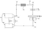
도 5는 본 발명에 따른 레이저 결정화 장치를 이용한 SLS 결정화 전체 공정도를 나타낸 도면이다.5 is a view showing the overall process of SLS crystallization using a laser crystallization apparatus according to the present invention.
도시한 바와 같이, 절연기판(100)과, 절연기판(100) 상부에 형성된 비정질 실리콘 박막(102)으로 구성된 기판(104)이 구비되고, 상기 비정질 실리콘 박막(102)을 단결정 실리콘 박막으로 결정화하기 위한 레이저 결정화 장치(110)는 펄스 레이저 빔(112a)을 조사하는 제 1 레이저 장치(110a)와, 기판(104)의 하부쪽에서 CW 레이저 빔(112b ; continuous laser beam)을 조사하는 제 2 레이저 장치(110b)로 구성된다.As shown, a
이때, 상기 기판(104) 하부에는, 기판(104)을 X-Y 방향으로 일정하게 이동시키며, 상기 CW 레이저 빔(112b)을 투과시키는 패스홀(134 ; path hole)을 가지는 프리시젼 스테이지(134)가 배치되어 있다.In this case, a
좀 더 상세히 설명하면, 제 1 레이저 장치(110a)는 펄스 레이저 빔(112a)을 발생시키는 제 1 레이저 발생장치(114a)와, 펄스 레이저 빔(112a)의 형상을 가공하는 호모제나이저(116)와, 펄스 레이저 빔(112a)을 비정질 실리콘 박막(102) 상에 나누어 조사시키는 슬릿 마스크(118)와, 슬릿 마스크(118) 하부에 위치하여 펄스 레이저 빔(112a)의 에너지 밀도를 높이는 프로젝션 렌즈(120)로 구성된다.In more detail, the
그러나, 본 발명에서는 펄스 레이저 빔의 에너지 밀도를 높이는 역할을 렌지를 슬릿 마스크(118)를 사이에 두고 양쪽 또는 상부쪽에 배치하는 실시예도 포함한다.However, the present invention also includes an embodiment in which the stove is disposed on both sides or the upper side with the
그리고, 상기 제 2 레이저 장치(110b)는 상기 비정질 실리콘 박막(102)의 결정화를 돕기 위해, 상기 기판(104) 하부쪽으로 조사되는 CW 레이저 빔(112b)을 조사하는 제 2 레이저 발생장치(112b)를 뜻한다.In addition, the
상기 제 2 레이저 발생장치(112b)는 실리콘의 측면성장 길이 촉진을 위해 기판(104)을 예열시키는 목적으로 가지므로, 상기 제 1 레이저 장치(110a)보다 단순한 구성을 가지게 된다.Since the second laser generator 112b has a purpose of preheating the
이때, 상기 레이저 결정화 장치(110)에서는 레이저 빔(114)의 진행방향을 변경시키는 다수 개의 미러(122)를 포함한다.In this case, the
상기 펄스 레이저 빔(112a)은 엑시머(excimer) 레이저 빔으로 하는 것이 바람직하고, 상기 CW 레이저 빔(112b)은 아르곤(Ar) 레이저를 이용하는 것이 바람직하다. 그리고, 도면으로 제시하지는 않았지만, 상기 절연기판(100)과 비정질 실리콘 박막(102) 사이에는 실리콘 산화막(SiOx)으로 이루어진 버퍼층을 포함한다.The pulse laser beam 112a is preferably an excimer laser beam, and the CW laser beam 112b is preferably an argon (Ar) laser. Although not shown in the drawings, a buffer layer including a silicon oxide film (SiOx) is included between the insulating
또한, 상기 프리시젼 스테이지(134)에 형성된 패스홀(136)은 기판(104) 상에 조사되는 펄스 레이저 빔폭과 대응되거나 일정 간격 크게 할 수 있다.In addition, the
이와 같이, 본 발명에 따른 레이저 열처리 장치를 이용하여 SLS 결정화 공정을 진행하게 되면, 기판 하부쪽으로 또 다른 레이저 장치를 이용하여 기판을 예열한 후 실리콘 측면성장을 촉진하게 되므로, 실리콘의 측면성장 길이를 보다 길게 할 수 있어, 신뢰성 높은 단결정 실리콘 박막을 얻을 수 있다.As such, when the SLS crystallization process is performed by using the laser heat treatment apparatus according to the present invention, the side growth length of the silicon is promoted after the preheating of the substrate using another laser apparatus toward the lower side of the substrate, thereby promoting silicon side growth. It can be made longer and a reliable single crystal silicon thin film can be obtained.
본 발명은 상기 실시예로 한정하지 않으며, 본 발명의 취지에 벗어나지 않는 범위내에서 다양하게 변경하여 실시할 수 있다.The present invention is not limited to the above embodiments, and various modifications can be made without departing from the spirit of the present invention.
이와 같이, 본 발명에 따른 레이저 장치를 이용한 SLS 결정화 공정에 의하면, 실리콘 박막의 결정화 특성 향상으로 전기적 특성이 향상된 박막트랜지스터를 제공할 수 있으며, SLS 결정화 공정 처리량(throughput) 증가를 통해 생산성을 높일 수 있는 효과를 가진다.As such, according to the SLS crystallization process using the laser device according to the present invention, it is possible to provide a thin film transistor with improved electrical properties by improving the crystallization characteristics of the silicon thin film, and to increase productivity through an increase in throughput of the SLS crystallization process. Has the effect.
삭제delete
Claims (6)
Translated fromKoreanPriority Applications (1)
| Application Number | Priority Date | Filing Date | Title |
|---|---|---|---|
| KR1020010086423AKR100611040B1 (en) | 2001-12-27 | 2001-12-27 | Laser heat treatment device |
Applications Claiming Priority (1)
| Application Number | Priority Date | Filing Date | Title |
|---|---|---|---|
| KR1020010086423AKR100611040B1 (en) | 2001-12-27 | 2001-12-27 | Laser heat treatment device |
Publications (2)
| Publication Number | Publication Date |
|---|---|
| KR20030056248A KR20030056248A (en) | 2003-07-04 |
| KR100611040B1true KR100611040B1 (en) | 2006-08-09 |
Family
ID=32214458
Family Applications (1)
| Application Number | Title | Priority Date | Filing Date |
|---|---|---|---|
| KR1020010086423AExpired - Fee RelatedKR100611040B1 (en) | 2001-12-27 | 2001-12-27 | Laser heat treatment device |
Country Status (1)
| Country | Link |
|---|---|
| KR (1) | KR100611040B1 (en) |
Families Citing this family (7)
| Publication number | Priority date | Publication date | Assignee | Title |
|---|---|---|---|---|
| JP2005167084A (en)* | 2003-12-04 | 2005-06-23 | Fujitsu Ltd | Laser crystallization apparatus and laser crystallization method |
| KR100603330B1 (en)* | 2004-02-16 | 2006-07-20 | 삼성에스디아이 주식회사 | Laser crystallization device |
| KR101034959B1 (en)* | 2004-03-17 | 2011-05-17 | 엘지디스플레이 주식회사 | Repair device and repair method for repairing metal line defects |
| KR100643308B1 (en) | 2005-07-11 | 2006-11-10 | 삼성전자주식회사 | Apparatus and method for providing music file navigation |
| KR100814821B1 (en)* | 2006-09-19 | 2008-03-20 | 삼성에스디아이 주식회사 | Crystallization Apparatus and Method of Silicon Thin Film |
| KR101000067B1 (en)* | 2008-12-30 | 2010-12-10 | 엘지전자 주식회사 | Laser firing apparatus for high efficiency solar cell and manufacturing method of high efficiency solar cell |
| TWI624862B (en) | 2012-06-11 | 2018-05-21 | 應用材料股份有限公司 | Melt depth determination using infrared interferometric technique in pulsed laser annealing |
Citations (5)
| Publication number | Priority date | Publication date | Assignee | Title |
|---|---|---|---|---|
| JPS63233518A (en)* | 1987-03-23 | 1988-09-29 | Agency Of Ind Science & Technol | Apparatus for forming single crystal thin film |
| JPH0521340A (en)* | 1991-07-10 | 1993-01-29 | Ricoh Co Ltd | Thin film semiconductor device, manufacturing method thereof and manufacturing device |
| JPH06120139A (en)* | 1992-10-05 | 1994-04-28 | Ricoh Co Ltd | Semiconductor material manufacturing equipment |
| JPH07118087A (en)* | 1993-10-20 | 1995-05-09 | Niyuuraru Syst:Kk | Formation of single crystal thin film |
| KR20000011334A (en)* | 1998-07-13 | 2000-02-25 | 아끼구사 나오유끼 | Polycrystal thin film forming method and forming system |
- 2001
- 2001-12-27KRKR1020010086423Apatent/KR100611040B1/ennot_activeExpired - Fee Related
Patent Citations (5)
| Publication number | Priority date | Publication date | Assignee | Title |
|---|---|---|---|---|
| JPS63233518A (en)* | 1987-03-23 | 1988-09-29 | Agency Of Ind Science & Technol | Apparatus for forming single crystal thin film |
| JPH0521340A (en)* | 1991-07-10 | 1993-01-29 | Ricoh Co Ltd | Thin film semiconductor device, manufacturing method thereof and manufacturing device |
| JPH06120139A (en)* | 1992-10-05 | 1994-04-28 | Ricoh Co Ltd | Semiconductor material manufacturing equipment |
| JPH07118087A (en)* | 1993-10-20 | 1995-05-09 | Niyuuraru Syst:Kk | Formation of single crystal thin film |
| KR20000011334A (en)* | 1998-07-13 | 2000-02-25 | 아끼구사 나오유끼 | Polycrystal thin film forming method and forming system |
Also Published As
| Publication number | Publication date |
|---|---|
| KR20030056248A (en) | 2003-07-04 |
Similar Documents
| Publication | Publication Date | Title |
|---|---|---|
| US8598588B2 (en) | Systems and methods for processing a film, and thin films | |
| CN1614756B (en) | Semiconductor device and its manufacture | |
| US6821343B2 (en) | Semiconductor device, manufacturing method therefor, and semiconductor manufacturing apparatus | |
| CN100372058C (en) | Laser beam pattern mask and crystallization method using it | |
| TWI402989B (en) | Method for forming polycrystalline germanium film and method for manufacturing thin film transistor using the same | |
| US6573163B2 (en) | Method of optimizing channel characteristics using multiple masks to form laterally crystallized ELA poly-Si films | |
| JP4211967B2 (en) | Method for crystallizing silicon using mask | |
| US20090218577A1 (en) | High throughput crystallization of thin films | |
| CN101184871A (en) | Line-scan sequential lateral curing of thin films | |
| US6686978B2 (en) | Method of forming an LCD with predominantly <100> polycrystalline silicon regions | |
| US20020102821A1 (en) | Mask pattern design to improve quality uniformity in lateral laser crystallized poly-Si films | |
| US20030148566A1 (en) | Production method for flat panel display | |
| KR100611040B1 (en) | Laser heat treatment device | |
| EP1860699A1 (en) | Display having thin fim transistors with channel region of varying crystal state | |
| US8614471B2 (en) | Collections of laterally crystallized semiconductor islands for use in thin film transistors | |
| JP2002057105A (en) | Method and device for manufacturing semiconductor thin film, and matrix circuit-driving device | |
| KR100761346B1 (en) | Method for producing crystalline silicon | |
| JP2006295117A (en) | Method for manufacturing polycrystalline silicon thin film and method for manufacturing thin film transistor having the same | |
| KR20030015617A (en) | Method of manufacturing a crystalloid silicone | |
| KR100860007B1 (en) | Thin film transistor, manufacturing method of thin film transistor, organic light emitting display device having same and manufacturing method thereof | |
| KR20060106170A (en) | Method for manufacturing polycrystalline silicon thin film and method for manufacturing thin film transistor having same | |
| JP4467276B2 (en) | Method and apparatus for manufacturing semiconductor thin films | |
| JPH0566422A (en) | Production of liquid crystal display device and production of sensor | |
| KR20060131518A (en) | Laser Crystallization System, Laser Crystallization Method and Manufacturing Method of Thin Film Transistor Substrate for Liquid Crystal Display Using Same | |
| JP2005039259A (en) | Crystallization method, crystallization equipment, thin-film transistor (tft), and display device |
Legal Events
| Date | Code | Title | Description |
|---|---|---|---|
| A201 | Request for examination | ||
| PA0109 | Patent application | St.27 status event code:A-0-1-A10-A12-nap-PA0109 | |
| PA0201 | Request for examination | St.27 status event code:A-1-2-D10-D11-exm-PA0201 | |
| PG1501 | Laying open of application | St.27 status event code:A-1-1-Q10-Q12-nap-PG1501 | |
| D13-X000 | Search requested | St.27 status event code:A-1-2-D10-D13-srh-X000 | |
| D14-X000 | Search report completed | St.27 status event code:A-1-2-D10-D14-srh-X000 | |
| E902 | Notification of reason for refusal | ||
| PE0902 | Notice of grounds for rejection | St.27 status event code:A-1-2-D10-D21-exm-PE0902 | |
| P11-X000 | Amendment of application requested | St.27 status event code:A-2-2-P10-P11-nap-X000 | |
| P13-X000 | Application amended | St.27 status event code:A-2-2-P10-P13-nap-X000 | |
| R17-X000 | Change to representative recorded | St.27 status event code:A-3-3-R10-R17-oth-X000 | |
| E601 | Decision to refuse application | ||
| PE0601 | Decision on rejection of patent | St.27 status event code:N-2-6-B10-B15-exm-PE0601 | |
| J201 | Request for trial against refusal decision | ||
| PJ0201 | Trial against decision of rejection | St.27 status event code:A-3-3-V10-V11-apl-PJ0201 | |
| J301 | Trial decision | Free format text:TRIAL DECISION FOR APPEAL AGAINST DECISION TO DECLINE REFUSAL REQUESTED 20050218 Effective date:20060630 | |
| PJ1301 | Trial decision | St.27 status event code:A-3-3-V10-V15-crt-PJ1301 Decision date:20060630 Appeal event data comment text:Appeal Kind Category : Appeal against decision to decline refusal, Appeal Ground Text : 2001 86423 Appeal request date:20050218 Appellate body name:Patent Examination Board Decision authority category:Office appeal board Decision identifier:2005101001001 | |
| PS0901 | Examination by remand of revocation | St.27 status event code:A-6-3-E10-E12-rex-PS0901 | |
| S901 | Examination by remand of revocation | ||
| GRNO | Decision to grant (after opposition) | ||
| PS0701 | Decision of registration after remand of revocation | St.27 status event code:A-3-4-F10-F13-rex-PS0701 | |
| GRNT | Written decision to grant | ||
| PR0701 | Registration of establishment | St.27 status event code:A-2-4-F10-F11-exm-PR0701 | |
| PR1002 | Payment of registration fee | St.27 status event code:A-2-2-U10-U11-oth-PR1002 Fee payment year number:1 | |
| PG1601 | Publication of registration | St.27 status event code:A-4-4-Q10-Q13-nap-PG1601 | |
| PN2301 | Change of applicant | St.27 status event code:A-5-5-R10-R13-asn-PN2301 St.27 status event code:A-5-5-R10-R11-asn-PN2301 | |
| PR1001 | Payment of annual fee | St.27 status event code:A-4-4-U10-U11-oth-PR1001 Fee payment year number:4 | |
| PR1001 | Payment of annual fee | St.27 status event code:A-4-4-U10-U11-oth-PR1001 Fee payment year number:5 | |
| R18-X000 | Changes to party contact information recorded | St.27 status event code:A-5-5-R10-R18-oth-X000 | |
| PR1001 | Payment of annual fee | St.27 status event code:A-4-4-U10-U11-oth-PR1001 Fee payment year number:6 | |
| R18-X000 | Changes to party contact information recorded | St.27 status event code:A-5-5-R10-R18-oth-X000 | |
| R18-X000 | Changes to party contact information recorded | St.27 status event code:A-5-5-R10-R18-oth-X000 | |
| PR1001 | Payment of annual fee | St.27 status event code:A-4-4-U10-U11-oth-PR1001 Fee payment year number:7 | |
| FPAY | Annual fee payment | Payment date:20130619 Year of fee payment:8 | |
| PR1001 | Payment of annual fee | St.27 status event code:A-4-4-U10-U11-oth-PR1001 Fee payment year number:8 | |
| FPAY | Annual fee payment | Payment date:20140630 Year of fee payment:9 | |
| PR1001 | Payment of annual fee | St.27 status event code:A-4-4-U10-U11-oth-PR1001 Fee payment year number:9 | |
| FPAY | Annual fee payment | Payment date:20150728 Year of fee payment:10 | |
| PR1001 | Payment of annual fee | St.27 status event code:A-4-4-U10-U11-oth-PR1001 Fee payment year number:10 | |
| FPAY | Annual fee payment | Payment date:20160712 Year of fee payment:11 | |
| PR1001 | Payment of annual fee | St.27 status event code:A-4-4-U10-U11-oth-PR1001 Fee payment year number:11 | |
| P22-X000 | Classification modified | St.27 status event code:A-4-4-P10-P22-nap-X000 | |
| FPAY | Annual fee payment | Payment date:20170713 Year of fee payment:12 | |
| PR1001 | Payment of annual fee | St.27 status event code:A-4-4-U10-U11-oth-PR1001 Fee payment year number:12 | |
| PR1001 | Payment of annual fee | St.27 status event code:A-4-4-U10-U11-oth-PR1001 Fee payment year number:13 | |
| PC1903 | Unpaid annual fee | St.27 status event code:A-4-4-U10-U13-oth-PC1903 Not in force date:20190804 Payment event data comment text:Termination Category : DEFAULT_OF_REGISTRATION_FEE | |
| PC1903 | Unpaid annual fee | St.27 status event code:N-4-6-H10-H13-oth-PC1903 Ip right cessation event data comment text:Termination Category : DEFAULT_OF_REGISTRATION_FEE Not in force date:20190804 |