KR100608610B1 - Printed circuit board, manufacturing method thereof and semiconductor package using same - Google Patents
Printed circuit board, manufacturing method thereof and semiconductor package using sameDownload PDFInfo
- Publication number
- KR100608610B1 KR100608610B1KR1020040108782AKR20040108782AKR100608610B1KR 100608610 B1KR100608610 B1KR 100608610B1KR 1020040108782 AKR1020040108782 AKR 1020040108782AKR 20040108782 AKR20040108782 AKR 20040108782AKR 100608610 B1KR100608610 B1KR 100608610B1
- Authority
- KR
- South Korea
- Prior art keywords
- wiring layer
- substrate body
- printed circuit
- layer
- circuit board
- Prior art date
- Legal status (The legal status is an assumption and is not a legal conclusion. Google has not performed a legal analysis and makes no representation as to the accuracy of the status listed.)
- Expired - Fee Related
Links
Images


Classifications
- H—ELECTRICITY
- H01—ELECTRIC ELEMENTS
- H01L—SEMICONDUCTOR DEVICES NOT COVERED BY CLASS H10
- H01L23/00—Details of semiconductor or other solid state devices
- H01L23/48—Arrangements for conducting electric current to or from the solid state body in operation, e.g. leads, terminal arrangements ; Selection of materials therefor
- H01L23/50—Arrangements for conducting electric current to or from the solid state body in operation, e.g. leads, terminal arrangements ; Selection of materials therefor for integrated circuit devices, e.g. power bus, number of leads
- H—ELECTRICITY
- H01—ELECTRIC ELEMENTS
- H01L—SEMICONDUCTOR DEVICES NOT COVERED BY CLASS H10
- H01L23/00—Details of semiconductor or other solid state devices
- H01L23/28—Encapsulations, e.g. encapsulating layers, coatings, e.g. for protection
- H01L23/31—Encapsulations, e.g. encapsulating layers, coatings, e.g. for protection characterised by the arrangement or shape
- H01L23/3107—Encapsulations, e.g. encapsulating layers, coatings, e.g. for protection characterised by the arrangement or shape the device being completely enclosed
- H01L23/3121—Encapsulations, e.g. encapsulating layers, coatings, e.g. for protection characterised by the arrangement or shape the device being completely enclosed a substrate forming part of the encapsulation
- H01L23/3128—Encapsulations, e.g. encapsulating layers, coatings, e.g. for protection characterised by the arrangement or shape the device being completely enclosed a substrate forming part of the encapsulation the substrate having spherical bumps for external connection
- H—ELECTRICITY
- H01—ELECTRIC ELEMENTS
- H01L—SEMICONDUCTOR DEVICES NOT COVERED BY CLASS H10
- H01L21/00—Processes or apparatus adapted for the manufacture or treatment of semiconductor or solid state devices or of parts thereof
- H01L21/02—Manufacture or treatment of semiconductor devices or of parts thereof
- H01L21/04—Manufacture or treatment of semiconductor devices or of parts thereof the devices having potential barriers, e.g. a PN junction, depletion layer or carrier concentration layer
- H01L21/48—Manufacture or treatment of parts, e.g. containers, prior to assembly of the devices, using processes not provided for in a single one of the groups H01L21/18 - H01L21/326 or H10D48/04 - H10D48/07
- H01L21/4814—Conductive parts
- H01L21/4846—Leads on or in insulating or insulated substrates, e.g. metallisation
- H01L21/4857—Multilayer substrates
- H—ELECTRICITY
- H01—ELECTRIC ELEMENTS
- H01L—SEMICONDUCTOR DEVICES NOT COVERED BY CLASS H10
- H01L23/00—Details of semiconductor or other solid state devices
- H01L23/48—Arrangements for conducting electric current to or from the solid state body in operation, e.g. leads, terminal arrangements ; Selection of materials therefor
- H01L23/488—Arrangements for conducting electric current to or from the solid state body in operation, e.g. leads, terminal arrangements ; Selection of materials therefor consisting of soldered or bonded constructions
- H01L23/498—Leads, i.e. metallisations or lead-frames on insulating substrates, e.g. chip carriers
- H01L23/49811—Additional leads joined to the metallisation on the insulating substrate, e.g. pins, bumps, wires, flat leads
- H01L23/49816—Spherical bumps on the substrate for external connection, e.g. ball grid arrays [BGA]
- H—ELECTRICITY
- H01—ELECTRIC ELEMENTS
- H01L—SEMICONDUCTOR DEVICES NOT COVERED BY CLASS H10
- H01L23/00—Details of semiconductor or other solid state devices
- H01L23/564—Details not otherwise provided for, e.g. protection against moisture
- H—ELECTRICITY
- H01—ELECTRIC ELEMENTS
- H01L—SEMICONDUCTOR DEVICES NOT COVERED BY CLASS H10
- H01L24/00—Arrangements for connecting or disconnecting semiconductor or solid-state bodies; Methods or apparatus related thereto
- H01L24/01—Means for bonding being attached to, or being formed on, the surface to be connected, e.g. chip-to-package, die-attach, "first-level" interconnects; Manufacturing methods related thereto
- H01L24/26—Layer connectors, e.g. plate connectors, solder or adhesive layers; Manufacturing methods related thereto
- H01L24/31—Structure, shape, material or disposition of the layer connectors after the connecting process
- H01L24/32—Structure, shape, material or disposition of the layer connectors after the connecting process of an individual layer connector
- H—ELECTRICITY
- H05—ELECTRIC TECHNIQUES NOT OTHERWISE PROVIDED FOR
- H05K—PRINTED CIRCUITS; CASINGS OR CONSTRUCTIONAL DETAILS OF ELECTRIC APPARATUS; MANUFACTURE OF ASSEMBLAGES OF ELECTRICAL COMPONENTS
- H05K3/00—Apparatus or processes for manufacturing printed circuits
- H05K3/22—Secondary treatment of printed circuits
- H05K3/28—Applying non-metallic protective coatings
- H05K3/281—Applying non-metallic protective coatings by means of a preformed insulating foil
- H—ELECTRICITY
- H01—ELECTRIC ELEMENTS
- H01L—SEMICONDUCTOR DEVICES NOT COVERED BY CLASS H10
- H01L21/00—Processes or apparatus adapted for the manufacture or treatment of semiconductor or solid state devices or of parts thereof
- H01L21/67—Apparatus specially adapted for handling semiconductor or electric solid state devices during manufacture or treatment thereof; Apparatus specially adapted for handling wafers during manufacture or treatment of semiconductor or electric solid state devices or components ; Apparatus not specifically provided for elsewhere
- H01L21/683—Apparatus specially adapted for handling semiconductor or electric solid state devices during manufacture or treatment thereof; Apparatus specially adapted for handling wafers during manufacture or treatment of semiconductor or electric solid state devices or components ; Apparatus not specifically provided for elsewhere for supporting or gripping
- H01L21/6835—Apparatus specially adapted for handling semiconductor or electric solid state devices during manufacture or treatment thereof; Apparatus specially adapted for handling wafers during manufacture or treatment of semiconductor or electric solid state devices or components ; Apparatus not specifically provided for elsewhere for supporting or gripping using temporarily an auxiliary support
- H—ELECTRICITY
- H01—ELECTRIC ELEMENTS
- H01L—SEMICONDUCTOR DEVICES NOT COVERED BY CLASS H10
- H01L2224/00—Indexing scheme for arrangements for connecting or disconnecting semiconductor or solid-state bodies and methods related thereto as covered by H01L24/00
- H01L2224/01—Means for bonding being attached to, or being formed on, the surface to be connected, e.g. chip-to-package, die-attach, "first-level" interconnects; Manufacturing methods related thereto
- H01L2224/26—Layer connectors, e.g. plate connectors, solder or adhesive layers; Manufacturing methods related thereto
- H01L2224/31—Structure, shape, material or disposition of the layer connectors after the connecting process
- H01L2224/32—Structure, shape, material or disposition of the layer connectors after the connecting process of an individual layer connector
- H01L2224/3205—Shape
- H01L2224/32057—Shape in side view
- H—ELECTRICITY
- H01—ELECTRIC ELEMENTS
- H01L—SEMICONDUCTOR DEVICES NOT COVERED BY CLASS H10
- H01L2224/00—Indexing scheme for arrangements for connecting or disconnecting semiconductor or solid-state bodies and methods related thereto as covered by H01L24/00
- H01L2224/01—Means for bonding being attached to, or being formed on, the surface to be connected, e.g. chip-to-package, die-attach, "first-level" interconnects; Manufacturing methods related thereto
- H01L2224/26—Layer connectors, e.g. plate connectors, solder or adhesive layers; Manufacturing methods related thereto
- H01L2224/31—Structure, shape, material or disposition of the layer connectors after the connecting process
- H01L2224/32—Structure, shape, material or disposition of the layer connectors after the connecting process of an individual layer connector
- H01L2224/321—Disposition
- H01L2224/32151—Disposition the layer connector connecting between a semiconductor or solid-state body and an item not being a semiconductor or solid-state body, e.g. chip-to-substrate, chip-to-passive
- H01L2224/32221—Disposition the layer connector connecting between a semiconductor or solid-state body and an item not being a semiconductor or solid-state body, e.g. chip-to-substrate, chip-to-passive the body and the item being stacked
- H01L2224/32225—Disposition the layer connector connecting between a semiconductor or solid-state body and an item not being a semiconductor or solid-state body, e.g. chip-to-substrate, chip-to-passive the body and the item being stacked the item being non-metallic, e.g. insulating substrate with or without metallisation
- H—ELECTRICITY
- H01—ELECTRIC ELEMENTS
- H01L—SEMICONDUCTOR DEVICES NOT COVERED BY CLASS H10
- H01L2224/00—Indexing scheme for arrangements for connecting or disconnecting semiconductor or solid-state bodies and methods related thereto as covered by H01L24/00
- H01L2224/01—Means for bonding being attached to, or being formed on, the surface to be connected, e.g. chip-to-package, die-attach, "first-level" interconnects; Manufacturing methods related thereto
- H01L2224/42—Wire connectors; Manufacturing methods related thereto
- H01L2224/47—Structure, shape, material or disposition of the wire connectors after the connecting process
- H01L2224/48—Structure, shape, material or disposition of the wire connectors after the connecting process of an individual wire connector
- H01L2224/4805—Shape
- H01L2224/4809—Loop shape
- H01L2224/48091—Arched
- H—ELECTRICITY
- H01—ELECTRIC ELEMENTS
- H01L—SEMICONDUCTOR DEVICES NOT COVERED BY CLASS H10
- H01L2224/00—Indexing scheme for arrangements for connecting or disconnecting semiconductor or solid-state bodies and methods related thereto as covered by H01L24/00
- H01L2224/01—Means for bonding being attached to, or being formed on, the surface to be connected, e.g. chip-to-package, die-attach, "first-level" interconnects; Manufacturing methods related thereto
- H01L2224/42—Wire connectors; Manufacturing methods related thereto
- H01L2224/47—Structure, shape, material or disposition of the wire connectors after the connecting process
- H01L2224/48—Structure, shape, material or disposition of the wire connectors after the connecting process of an individual wire connector
- H01L2224/4805—Shape
- H01L2224/4809—Loop shape
- H01L2224/48095—Kinked
- H—ELECTRICITY
- H01—ELECTRIC ELEMENTS
- H01L—SEMICONDUCTOR DEVICES NOT COVERED BY CLASS H10
- H01L2224/00—Indexing scheme for arrangements for connecting or disconnecting semiconductor or solid-state bodies and methods related thereto as covered by H01L24/00
- H01L2224/01—Means for bonding being attached to, or being formed on, the surface to be connected, e.g. chip-to-package, die-attach, "first-level" interconnects; Manufacturing methods related thereto
- H01L2224/42—Wire connectors; Manufacturing methods related thereto
- H01L2224/47—Structure, shape, material or disposition of the wire connectors after the connecting process
- H01L2224/48—Structure, shape, material or disposition of the wire connectors after the connecting process of an individual wire connector
- H01L2224/481—Disposition
- H01L2224/48151—Connecting between a semiconductor or solid-state body and an item not being a semiconductor or solid-state body, e.g. chip-to-substrate, chip-to-passive
- H01L2224/48221—Connecting between a semiconductor or solid-state body and an item not being a semiconductor or solid-state body, e.g. chip-to-substrate, chip-to-passive the body and the item being stacked
- H01L2224/48225—Connecting between a semiconductor or solid-state body and an item not being a semiconductor or solid-state body, e.g. chip-to-substrate, chip-to-passive the body and the item being stacked the item being non-metallic, e.g. insulating substrate with or without metallisation
- H01L2224/48227—Connecting between a semiconductor or solid-state body and an item not being a semiconductor or solid-state body, e.g. chip-to-substrate, chip-to-passive the body and the item being stacked the item being non-metallic, e.g. insulating substrate with or without metallisation connecting the wire to a bond pad of the item
- H—ELECTRICITY
- H01—ELECTRIC ELEMENTS
- H01L—SEMICONDUCTOR DEVICES NOT COVERED BY CLASS H10
- H01L2224/00—Indexing scheme for arrangements for connecting or disconnecting semiconductor or solid-state bodies and methods related thereto as covered by H01L24/00
- H01L2224/01—Means for bonding being attached to, or being formed on, the surface to be connected, e.g. chip-to-package, die-attach, "first-level" interconnects; Manufacturing methods related thereto
- H01L2224/42—Wire connectors; Manufacturing methods related thereto
- H01L2224/47—Structure, shape, material or disposition of the wire connectors after the connecting process
- H01L2224/48—Structure, shape, material or disposition of the wire connectors after the connecting process of an individual wire connector
- H01L2224/484—Connecting portions
- H01L2224/48463—Connecting portions the connecting portion on the bonding area of the semiconductor or solid-state body being a ball bond
- H—ELECTRICITY
- H01—ELECTRIC ELEMENTS
- H01L—SEMICONDUCTOR DEVICES NOT COVERED BY CLASS H10
- H01L2224/00—Indexing scheme for arrangements for connecting or disconnecting semiconductor or solid-state bodies and methods related thereto as covered by H01L24/00
- H01L2224/73—Means for bonding being of different types provided for in two or more of groups H01L2224/10, H01L2224/18, H01L2224/26, H01L2224/34, H01L2224/42, H01L2224/50, H01L2224/63, H01L2224/71
- H01L2224/732—Location after the connecting process
- H01L2224/73251—Location after the connecting process on different surfaces
- H01L2224/73265—Layer and wire connectors
- H—ELECTRICITY
- H01—ELECTRIC ELEMENTS
- H01L—SEMICONDUCTOR DEVICES NOT COVERED BY CLASS H10
- H01L2224/00—Indexing scheme for arrangements for connecting or disconnecting semiconductor or solid-state bodies and methods related thereto as covered by H01L24/00
- H01L2224/80—Methods for connecting semiconductor or other solid state bodies using means for bonding being attached to, or being formed on, the surface to be connected
- H01L2224/83—Methods for connecting semiconductor or other solid state bodies using means for bonding being attached to, or being formed on, the surface to be connected using a layer connector
- H01L2224/8338—Bonding interfaces outside the semiconductor or solid-state body
- H01L2224/83385—Shape, e.g. interlocking features
- H—ELECTRICITY
- H01—ELECTRIC ELEMENTS
- H01L—SEMICONDUCTOR DEVICES NOT COVERED BY CLASS H10
- H01L24/00—Arrangements for connecting or disconnecting semiconductor or solid-state bodies; Methods or apparatus related thereto
- H01L24/01—Means for bonding being attached to, or being formed on, the surface to be connected, e.g. chip-to-package, die-attach, "first-level" interconnects; Manufacturing methods related thereto
- H01L24/42—Wire connectors; Manufacturing methods related thereto
- H01L24/47—Structure, shape, material or disposition of the wire connectors after the connecting process
- H01L24/48—Structure, shape, material or disposition of the wire connectors after the connecting process of an individual wire connector
- H—ELECTRICITY
- H01—ELECTRIC ELEMENTS
- H01L—SEMICONDUCTOR DEVICES NOT COVERED BY CLASS H10
- H01L24/00—Arrangements for connecting or disconnecting semiconductor or solid-state bodies; Methods or apparatus related thereto
- H01L24/73—Means for bonding being of different types provided for in two or more of groups H01L24/10, H01L24/18, H01L24/26, H01L24/34, H01L24/42, H01L24/50, H01L24/63, H01L24/71
- H—ELECTRICITY
- H01—ELECTRIC ELEMENTS
- H01L—SEMICONDUCTOR DEVICES NOT COVERED BY CLASS H10
- H01L2924/00—Indexing scheme for arrangements or methods for connecting or disconnecting semiconductor or solid-state bodies as covered by H01L24/00
- H01L2924/0001—Technical content checked by a classifier
- H01L2924/00014—Technical content checked by a classifier the subject-matter covered by the group, the symbol of which is combined with the symbol of this group, being disclosed without further technical details
- H—ELECTRICITY
- H01—ELECTRIC ELEMENTS
- H01L—SEMICONDUCTOR DEVICES NOT COVERED BY CLASS H10
- H01L2924/00—Indexing scheme for arrangements or methods for connecting or disconnecting semiconductor or solid-state bodies as covered by H01L24/00
- H01L2924/01—Chemical elements
- H01L2924/01005—Boron [B]
- H—ELECTRICITY
- H01—ELECTRIC ELEMENTS
- H01L—SEMICONDUCTOR DEVICES NOT COVERED BY CLASS H10
- H01L2924/00—Indexing scheme for arrangements or methods for connecting or disconnecting semiconductor or solid-state bodies as covered by H01L24/00
- H01L2924/01—Chemical elements
- H01L2924/01006—Carbon [C]
- H—ELECTRICITY
- H01—ELECTRIC ELEMENTS
- H01L—SEMICONDUCTOR DEVICES NOT COVERED BY CLASS H10
- H01L2924/00—Indexing scheme for arrangements or methods for connecting or disconnecting semiconductor or solid-state bodies as covered by H01L24/00
- H01L2924/01—Chemical elements
- H01L2924/01023—Vanadium [V]
- H—ELECTRICITY
- H01—ELECTRIC ELEMENTS
- H01L—SEMICONDUCTOR DEVICES NOT COVERED BY CLASS H10
- H01L2924/00—Indexing scheme for arrangements or methods for connecting or disconnecting semiconductor or solid-state bodies as covered by H01L24/00
- H01L2924/01—Chemical elements
- H01L2924/01029—Copper [Cu]
- H—ELECTRICITY
- H01—ELECTRIC ELEMENTS
- H01L—SEMICONDUCTOR DEVICES NOT COVERED BY CLASS H10
- H01L2924/00—Indexing scheme for arrangements or methods for connecting or disconnecting semiconductor or solid-state bodies as covered by H01L24/00
- H01L2924/01—Chemical elements
- H01L2924/01033—Arsenic [As]
- H—ELECTRICITY
- H01—ELECTRIC ELEMENTS
- H01L—SEMICONDUCTOR DEVICES NOT COVERED BY CLASS H10
- H01L2924/00—Indexing scheme for arrangements or methods for connecting or disconnecting semiconductor or solid-state bodies as covered by H01L24/00
- H01L2924/01—Chemical elements
- H01L2924/01082—Lead [Pb]
- H—ELECTRICITY
- H01—ELECTRIC ELEMENTS
- H01L—SEMICONDUCTOR DEVICES NOT COVERED BY CLASS H10
- H01L2924/00—Indexing scheme for arrangements or methods for connecting or disconnecting semiconductor or solid-state bodies as covered by H01L24/00
- H01L2924/15—Details of package parts other than the semiconductor or other solid state devices to be connected
- H01L2924/151—Die mounting substrate
- H01L2924/153—Connection portion
- H01L2924/1531—Connection portion the connection portion being formed only on the surface of the substrate opposite to the die mounting surface
- H01L2924/15311—Connection portion the connection portion being formed only on the surface of the substrate opposite to the die mounting surface being a ball array, e.g. BGA
- H—ELECTRICITY
- H01—ELECTRIC ELEMENTS
- H01L—SEMICONDUCTOR DEVICES NOT COVERED BY CLASS H10
- H01L2924/00—Indexing scheme for arrangements or methods for connecting or disconnecting semiconductor or solid-state bodies as covered by H01L24/00
- H01L2924/15—Details of package parts other than the semiconductor or other solid state devices to be connected
- H01L2924/181—Encapsulation
- H—ELECTRICITY
- H05—ELECTRIC TECHNIQUES NOT OTHERWISE PROVIDED FOR
- H05K—PRINTED CIRCUITS; CASINGS OR CONSTRUCTIONAL DETAILS OF ELECTRIC APPARATUS; MANUFACTURE OF ASSEMBLAGES OF ELECTRICAL COMPONENTS
- H05K2203/00—Indexing scheme relating to apparatus or processes for manufacturing printed circuits covered by H05K3/00
- H05K2203/06—Lamination
- H05K2203/063—Lamination of preperforated insulating layer
- H—ELECTRICITY
- H05—ELECTRIC TECHNIQUES NOT OTHERWISE PROVIDED FOR
- H05K—PRINTED CIRCUITS; CASINGS OR CONSTRUCTIONAL DETAILS OF ELECTRIC APPARATUS; MANUFACTURE OF ASSEMBLAGES OF ELECTRICAL COMPONENTS
- H05K2203/00—Indexing scheme relating to apparatus or processes for manufacturing printed circuits covered by H05K3/00
- H05K2203/11—Treatments characterised by their effect, e.g. heating, cooling, roughening
- H05K2203/1152—Replicating the surface structure of a sacrificial layer, e.g. for roughening
Landscapes
- Engineering & Computer Science (AREA)
- Microelectronics & Electronic Packaging (AREA)
- Computer Hardware Design (AREA)
- Power Engineering (AREA)
- Physics & Mathematics (AREA)
- Condensed Matter Physics & Semiconductors (AREA)
- General Physics & Mathematics (AREA)
- Manufacturing & Machinery (AREA)
- Ceramic Engineering (AREA)
- Non-Metallic Protective Coatings For Printed Circuits (AREA)
- Production Of Multi-Layered Print Wiring Board (AREA)
Abstract
Translated fromKoreanDescription
Translated fromKorean도 1은 종래기술에 따른 반도체 패키지용 인쇄회로기판을 보여주는 평면도이다.1 is a plan view showing a printed circuit board for a semiconductor package according to the prior art.
도 2는 도 1의 I-I선 단면도이다.FIG. 2 is a cross-sectional view taken along line II of FIG. 1.
도 3은 도 1의 인쇄회로기판을 이용한 반도체 패키지를 보여주는 단면도이다.3 is a cross-sectional view illustrating a semiconductor package using the printed circuit board of FIG. 1.
도 4 내지 도 9는 본 발명의 실시예에 따른 반도체 패키지용 인쇄회로기판의 제조 방법에 따른 단계를 보여주는 도면들로서,4 to 9 are diagrams showing steps according to a method of manufacturing a printed circuit board for a semiconductor package according to an embodiment of the present invention.
도 4는 기판 몸체에 구리 배선층이 형성된 상태를 보여주는 사시도이고,4 is a perspective view showing a state in which a copper wiring layer is formed on a substrate body;
도 5는 도 4의 Ⅱ-Ⅱ선 단면도이고,5 is a cross-sectional view taken along the line II-II of FIG. 4,
도 6은 기판 몸체의 상부면에 프리 프레그 시트가 탑재되는 단계를 보여주는 사시도이고,6 is a perspective view showing the step of mounting the prepreg sheet on the upper surface of the substrate body,
도 7은 기판 몸체의 상부면에 구리판을 열압착하여 프리 프레그 시트를 기판 몸체에 접착하는 단계를 보여주는 단면도이고,7 is a cross-sectional view showing a step of bonding the prepreg sheet to the substrate body by thermocompression bonding a copper plate on the upper surface of the substrate body,
도 8은 도 7의 Ⅲ-Ⅲ선 단면도이고,8 is a cross-sectional view taken along the line III-III of FIG. 7,
도 9는 도 8의 "A" 부분을 확대하여 보여주는 단면도이고,9 is an enlarged cross-sectional view of a portion “A” of FIG. 8,
도 10은 기판 몸체의 상부면에서 구리판을 제거하는 단계를 보여주는 단면도이고,10 is a cross-sectional view showing a step of removing a copper plate from the upper surface of the substrate body,
도 11은 기판 몸체의 하부면에 솔더 레지스트 층을 형성하는 단계를 단면도이다.11 is a cross-sectional view of forming a solder resist layer on a bottom surface of a substrate body.
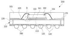
도 12는 도 11의 인쇄회로기판을 이용한 본 발명의 실시예에 따른 반도체 패키지를 보여주는 단면도이다.12 is a cross-sectional view illustrating a semiconductor package in accordance with an embodiment of the present invention using the printed circuit board of FIG. 11.
도 13은 도 12의 "B" 부분을 확대하여 보여주는 단면도이다.FIG. 13 is an enlarged cross-sectional view of part “B” of FIG. 12.
* 도면의 주요 부분에 대한 설명 *Description of the main parts of the drawing
110 : 기판 몸체 120 : 구리 배선층110: substrate body 120: copper wiring layer
122 : 상부 배선층 123 : 기판 패드122: upper wiring layer 123: substrate pad
124 : 하부 배선층 125 : 볼 패드124: lower wiring layer 125: ball pad
130 : 비아 홀 140 : 솔더 레지스트 층130: via hole 140: solder resist layer
150 : 인쇄회로기판 161 : 반도체 칩150: printed circuit board 161: semiconductor chip
162 : 칩 패드 163 : 접착제162: chip pad 163: adhesive
164 : 본딩 와이어 165 : 수지 봉합부164: bonding wire 165: resin sealing portion
166 : 솔더 볼 170 : 프리프레그 층166: solder ball 170: prepreg layer
172 : 프리프레그 시트 174 : 윈도우172: Prepreg Sheet 174: Windows
180 : 동박180: copper foil
본 발명은 인쇄회로기판과, 그의 제조 방법 및 그를 이용한 반도체 패키지에 관한 것으로, 더욱 상세하게는 인쇄회로기판을 구성하는 소재들 사이의 계면에서의 흡습을 억제하고 계면 접착력을 향상시킬 수 있는 인쇄회로기판과, 그의 제조 방법 및 그를 이용한 반도체 패키지에 관한 것이다.The present invention relates to a printed circuit board, a manufacturing method thereof, and a semiconductor package using the same. More particularly, the present invention relates to a printed circuit board capable of suppressing moisture absorption at an interface between materials constituting the printed circuit board and improving interface adhesion. It relates to a substrate, a method for manufacturing the same, and a semiconductor package using the same.
오늘날 전자산업의 추세는 더욱 경량화, 소형화, 고속화, 다기능화, 고성능화되고 높은 신뢰성을 갖는 제품을 저렴하게 제조하는 것이다. 이와 같은 제품 설계의 목표 달성을 가능하게 하는 중요한 기술 중의 하나가 바로 패키지 조립 기술이며, 이에 따라 근래에 개발된 패키지 중의 하나가 볼 그리드 어레이(Ball Grid Array; BGA) 패키지이다.The trend in today's electronics industry is to make products that are lighter, smaller, faster, more versatile, more efficient and more reliable. One of the important technologies that enables the achievement of this product design goal is package assembly technology, and one of the packages developed in recent years is a ball grid array (BGA) package.
BGA 패키지는 통상적인 플라스틱 패키지에 비하여, 모 기판(mother board)에 대한 실장 면적을 축소시킬 수 있고, 전기적 특성이 우수하다는 장점들을 갖고 있다. BGA 패키지는 통상적인 플라스틱 패키지와 달리 리드 프레임 대신에 인쇄회로기판을 사용한다. 인쇄회로기판은 반도체 칩이 접착되는 면의 반대쪽 전면을 솔더 볼(solder ball)들의 형성 영역으로 제공할 수 있기 때문에, 모 기판에 대한 실장 밀도 면에서 유리한 점이 있다.The BGA package has advantages in that the mounting area on the mother board can be reduced and the electrical characteristics are excellent, compared to the conventional plastic package. Unlike conventional plastic packages, BGA packages use printed circuit boards instead of lead frames. The printed circuit board has an advantage in terms of mounting density on the parent substrate because the printed circuit board can provide the front surface opposite to the surface where the semiconductor chip is bonded to the formation region of the solder balls.
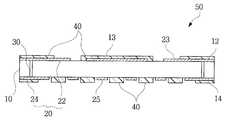
이와 같은 종래기술에 따른 BGA 패키지용 인쇄회로기판(50)은, 도 1 및 도 2에 도시된 바와 같이, 기판 몸체(10)의 양면(12, 14)에 구리 배선층(20)이 형성된 구조를 갖는다.The BGA package printed
인쇄회로기판(10)은 프리프레그(prepreg) 소재로 상부면(12)과 하부면(14)을 갖는 박형의 기판 몸체(10)를 형성하고, 양면(12, 14)에 얇은 동박을 접착하고, 접착된 동박을 패터닝하여 구리 배선층(20)이 형성된 구조를 갖는다. 구리 배선층(20)은 기판 몸체의 상부면(12)에 형성된 상부 배선층(22)과, 기판 몸체의 하부면(14)에 형성된 하부 배선층(24)으로 구성된다. 상부 배선층(22)은 기판 몸체의 상부면(12)의 중심 부분에 형성된 칩 실장 영역(13)에 근접하게 형성되어 반도체 칩과 전기적으로 연결될 기판 패드(23)를 포함한다. 하부 배선층(24)은 솔더 볼이 형성되는 볼 패드(25)를 포함한다. 기판 패드(23)와 볼 패드(25)는 기판 몸체(10)를 관통하여 형성된 비아 홀(30)에 의해 전기적으로 연결된다. 그리고 기판 몸체의 양면(12, 14)에 형성된 구리 배선층(20)을 외부환경으로부터 보호하기 위해서 보호층으로 솔더 레지스트 층(40; solder resist layer)을 기판 몸체의 양면(12, 14)을 덮도록 형성하게 되는데, 구리 배선층(20) 중에서 기판 패드(23)와 볼 패드(25)에는 형성되지 않는다.The printed
이때 솔더 레지스트 층(40)은 포토 솔더 레지스트(photo solder resist; PSR)를 기판 몸체의 양면(12, 14)에 균일한 두께로 코팅한 이후에 기판 패드(23)와 볼 패드(25)가 노출되도록 패터닝하여 형성하게 된다.In this case, the
이와 같은 구조를 갖는 인쇄회로기판(50)을 이용한 종래기술에 따른 BGA 패키지(100)가 도 3에 도시되어 있다. 도 3을 참조하면, 인쇄회로기판(50) 상부면의 칩 실장 영역(13)에 접착제(63)를 개재하여 반도체 칩(61)이 부착된다. 반도체 칩(61)의 칩 패드(62)와 기판 패드(23)는 본딩 와이어(64)에 의해 전기적으로 연결된다. 인쇄회로기판(50) 상부면에 형성된 반도체 칩(61)과 본딩 와이어(64)는 액상 의 성형 수지로 봉합하여 형성된 수지 봉합부(65)에 의해 보호된다. 그리고 인쇄회로기판(50) 하부면의 볼 패드(25)에 각기 솔더 볼(66)이 형성된다.A
이때 반도체 칩(61)이 인쇄회로기판(50)에 접착제(63)를 개재하여 접착될 때, 칩 실장 영역(13)에 형성된 솔더 레지스트 층(40) 위에 접착된다.At this time, when the
그런데 솔더 레지스트 층(40)의 소재는 포토 솔더 레지스트로서, 기판 몸체(10)에 균일하게 도포한 후 패터닝 공정을 통하여 쉽게 진행할 수 있는 특성을 갖고 있지만, 흡습성이 좋고 접착력이 떨어져 각종 문제를 야기한다.By the way, the material of the
즉 BGA 패키지(100)를 제조하는 과정에서 수지 봉합부(66)에 내포된 수분이 솔더 레지스트 층(40)으로 흡수되고, 제조된 BGA 패키지(100)에 대한 흡습 신뢰성 테스트에서 제공되는 수분이 솔더 레지스트 층(40)으로 흡수되기 때문에, 솔더 레지스트 층(40)과 계면을 이루는 부분에서 문제가 발생된다. 즉 솔더 레지스트 층(40)과 계면을 이루는 구리 배선층(20), 수지 봉합부(66), 접착제(63) 사이에서 발생되며, 특히 다층의 계면이 존재하는 반도체 칩(61) 아래에서 많이 발생된다.That is, moisture contained in the
구체적으로 설명하면, 먼저 솔더 레지스트 층(40)은 구리 배선층(20)과의 계면 접착력이 떨어진다. 그리고 솔더 레지스트 층(40)에 흡습된 수분은 BGA 패키지(100) 구동 중 발생되는 열과 외부에서 작용하는 고열에 의해 팽창하면서 계면이 부풀어 올라 솔더 레지스트 층(40)과 계면을 이루는 부분에서 박리나 크랙을 유발하게 된다.Specifically, first, the
이와 같은 문제점을 해소하기 위해서, 한국공개특허공보 제1999-62387호에 개시된 바와 같이, 솔더 레지스트 층을 통한 흡습 경로를 차단하고 수지 봉합부와 의 접착력을 강화시키기 위해서 솔더 레지스트 층에 요철 형태의 접착력 강화수단을 형성한 예가 개시되어 있다.In order to solve such a problem, as disclosed in Korean Patent Laid-Open Publication No. 1999-62387, in order to block the moisture absorption path through the solder resist layer and to strengthen the adhesive force with the resin sutures, the uneven form of adhesion to the solder resist layer An example of forming the reinforcing means is disclosed.
하지만 여전히 솔더 레지스트 층은 포토 솔더 레지스트를 소재로 사용함으로써, 포토 솔더 레지스트가 갖는 특성으로 인한 문제점은 그대로 안고 있다.However, the solder resist layer still uses the photo solder resist as a material, so the problem caused by the characteristics of the photo solder resist is still present.
따라서, 본 발명의 제 1 목적은 구리 배선층의 보호층으로 포토 솔더 레지스트를 대신하면서 인쇄회로기판를 구성하는 소재 사이의 양호한 계면 접착력을 확보할 수 있도록 하는 데 있다.Accordingly, a first object of the present invention is to ensure good interfacial adhesion between materials constituting the printed circuit board while replacing the photo solder resist with the protective layer of the copper wiring layer.
본 발명의 제 2 목적은 반도체 칩을 접착하는 접착제와 인쇄회로기판 사이의 양호한 계면 접착력을 확보할 수 있도록 하는 데 있다.A second object of the present invention is to ensure good interfacial adhesion between an adhesive for bonding a semiconductor chip and a printed circuit board.
본 발명의 제 3 목적은 포토 솔더 레지스트를 대신할 보호층의 소재로 기존의 인쇄회로기판 소재를 활용하여 새로운 소재 개발에 따른 비용 부담을 없도록 하는 데 있다.A third object of the present invention is to avoid the burden of developing a new material by using an existing printed circuit board material as a material of a protective layer to replace the photo solder resist.
상기 목적을 달성하기 위하여, (a) 소정의 두께를 갖는 기판 몸체를 준비하는 단계와; (b) 상기 기판 몸체의 양면에 구리 배선층을 형성하는 단계와; (c) 반도체 칩이 부착될 상기 기판 몸체의 상부면의 구리 배선층을 보호할 프리프레그 층을 형성하는 단계;를 포함하는 것을 특징으로 하는 반도체 패키지용 인쇄회로기판 제조 방법을 제공한다.In order to achieve the above object, (a) preparing a substrate body having a predetermined thickness; (b) forming copper wiring layers on both sides of the substrate body; (C) forming a prepreg layer to protect the copper wiring layer of the upper surface of the substrate body to which the semiconductor chip is attached; provides a printed circuit board manufacturing method for a semiconductor package comprising a.
본 발명에 따른 구리 배선층은 반도체 칩이 부착될 영역에 근접하게 형성된 기판 패드를 갖는 상부 배선층과, 상부 배선층과 전기적으로 연결되며 솔더 볼이 형성될 볼 패드를 갖는 하부 배선층을 포함한다.The copper wiring layer according to the present invention includes an upper wiring layer having a substrate pad formed adjacent to a region to which a semiconductor chip is attached, and a lower wiring layer having a ball pad electrically connected to the upper wiring layer and to which solder balls are to be formed.
본 발명에 따른 (c) 단계는, 기판 패드가 외부에 노출되도록 윈도우가 형성된 프리프레그 시트를 기판 몸체의 상부면에 탑재하는 단계와, 프리프레그 시트의 상부에 동박을 열압착하여 프리프레그 시트가 기판 몸체의 상부면에 열압착되어 상부 배선층을 보호하는 프리프레그 층을 형성하는 단계와, 프레프레그 층 위의 동박을 제거하는 단계를 포함한다.Step (c) according to the present invention comprises the steps of: mounting the prepreg sheet with a window formed on the upper surface of the substrate body so that the substrate pad is exposed to the outside; Forming a prepreg layer on the upper surface of the substrate body to protect the upper wiring layer; and removing copper foil on the prepreg layer.
본 발명에 따른 (c) 단계의 전 또는 후에 하부 배선층을 보호하기 위해서 볼 패드를 제외한 기판 몸체의 하부면을 덮는 솔더 레지스트 층을 형성하는 단계를 더 포함한다.Forming a solder resist layer covering the lower surface of the substrate body except for the ball pad to protect the lower wiring layer before or after step (c) according to the present invention.
본 발명에 따른 (b) 단계와 상기 (c) 단계 사이에, 상부 배선층과 하부 배선층을 전기적으로 연결하기 위해서 기판 몸체를 관통하는 비아 홀을 형성하는 단계를 더 포함한다.Between step (b) and step (c) according to the present invention, the method further includes forming a via hole penetrating the substrate body to electrically connect the upper wiring layer and the lower wiring layer.
본 발명은 또한 전술된 방법으로 제조된 인쇄회로기판을 제공한다. 즉, 상부면과, 상기 상부면에 반대되는 하부면을 갖는 소정의 두께를 갖는 기판 몸체와; 상기 기판 몸체의 양면에 형성된 구리 배선층과; 반도체 칩이 부착될 상기 기판 몸체 상부면에 형성되어 상기 구리 배선층을 보호하는 프리프레그 층;을 포함하는 것을 특징으로 하는 반도체 패키지용 인쇄회로기판을 제공한다.The present invention also provides a printed circuit board manufactured by the method described above. That is, a substrate body having an upper surface and a predetermined thickness having a lower surface opposite the upper surface; Copper wiring layers formed on both sides of the substrate body; And a prepreg layer formed on an upper surface of the substrate body to which a semiconductor chip is attached to protect the copper wiring layer.
본 발명은 또한 전술된 인쇄회로기판을 이용한 반도체 패키지를 제공한다. 즉, 활성면에 다수개의 칩 패드가 형성된 반도체 칩과; 상기 반도체 칩이 접착되 는 인쇄회로기판과; 상기 반도체 칩과 상기 인쇄회로기판을 전기적으로 연결하는 전기적 연결 수단과; 상기 인쇄회로기판 상부면의 반도체 칩과 전기적 연결 수단을 봉합하여 형성된 수지 봉합부와; 상기 인쇄회로기판의 하부면에 형성되며 상기 반도체 칩과 전기적으로 연결된 솔더 볼;을 포함하며,The present invention also provides a semiconductor package using the above-described printed circuit board. That is, a semiconductor chip having a plurality of chip pads formed on an active surface thereof; A printed circuit board to which the semiconductor chip is bonded; Electrical connection means for electrically connecting the semiconductor chip and the printed circuit board; A resin encapsulation portion formed by sealing a semiconductor chip and an electrical connection means on the upper surface of the printed circuit board; A solder ball formed on a lower surface of the printed circuit board and electrically connected to the semiconductor chip;
상기 인쇄회로기판은, 상기 반도체 칩이 접착되는 상부면과, 상기 상부면에 반대되는 하부면을 갖는 소정의 두께를 갖는 기판 몸체와; 상기 기판 몸체의 양면에 형성된 구리 배선층과; 상기 기판 몸체 상부면에 형성되어 상기 구리 배선층을 보호하는 프리프레그 층;을 포함하는 것을 특징으로 하는 인쇄회로기판을 이용한 반도체 패키지를 제공한다.The printed circuit board includes: a substrate body having a predetermined thickness having an upper surface to which the semiconductor chip is bonded and a lower surface opposite to the upper surface; Copper wiring layers formed on both sides of the substrate body; And a prepreg layer formed on the upper surface of the substrate body to protect the copper wiring layer.
이하, 첨부 도면을 참조하여 본 발명의 실시예를 보다 상세하게 설명하고자 한다.Hereinafter, with reference to the accompanying drawings will be described in detail an embodiment of the present invention.
도 4 내지 도 11은 본 발명의 실시예에 따른 반도체 패키지용 인쇄회로기판(150)의 제조 방법에 따른 단계를 보여주는 도면들이다. 한편 도면을 통틀어 동일한 도면부호는 동일한 구성요소를 나타낸다.4 to 11 illustrate the steps according to the method of manufacturing the printed
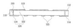
본 실시예의 제조 공정은, 도 4 및 도 5에 도시된 바와 같이, 양면(112, 114)에 구리 배선층(120)이 형성된 기판 몸체(110)를 준비하는 단계로부터 출발한다. 기판 몸체(110)는 소정의 두께를 갖는 프리프레그 소재의 절연판으로서, 소정의 두께의 프리프레그 시트(prepreg sheet)의 양면에 동박을 열압착한 후, 동박을 패터닝하여 구리 배선층(120)이 형성된 구조를 갖는다.4 and 5, the manufacturing process of the present embodiment starts from preparing a
구리 배선층(120)은 기판 몸체의 상부면(112)에 형성된 상부 배선층(122)과, 기판 몸체의 하부면(114)에 형성된 하부 배선층(124)으로 구성된다. 상부 배선층(122)은 기판 몸체 상부면(112)의 중심 부분에 형성될 칩 실장 영역에 근접하게 형성되어 반도체 칩과 전기적으로 연결되는 기판 패드(123)를 포함한다. 하부 배선층(124)은 솔더 볼이 형성되는 볼 패드(125)를 포함한다. 그리고 기판 패드(123)과 볼 패드(125)는 기판 몸체(110)를 관통하여 형성된 비아 홀(130)에 의해 전기적으로 연결된다.The
한편 본 발명의 실시예에 개시된 기판 몸체(110)는 하나의 반도체 패키지를 형성할 부분만을 개시하였지만, 다수개의 반도체 패키지를 함께 형성할 수 있는 매트릭스(matrix) 형태로 제공될 수 있다.Meanwhile, the
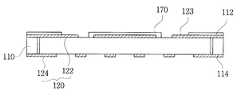
다음으로 도 6 내지 도 10에 도시된 바와 같이, 상부 배선층(122)의 보호층으로 기판 몸체의 상부면(112)에 프리프레그 층(170)을 형성하는 단계가 진행된다.Next, as shown in FIGS. 6 to 10, the
먼저 도 6에 도시된 바와 같이, 프리프레그 층으로 형성된 프리프레그 시트(172)를 기판 몸체의 상부면(112)에 탑재하는 단계가 진행된다. 프리프레그 시트(172)에는 기판 패드들(123)이 외부에 노출되도록 윈도우(174)가 형성되어 있다. 예컨대, 본 실시예에 따른 기판 몸체(110)의 네 변에 대응되게 기판 패드들(123)이 형성되어 있기 때문에, 각 변에 형성된 기판 패드들(123)이 일괄적으로 노출될 수 있도록 각기 윈도우(174)가 형성된 프리프레그 시트(172)를 사용하였다.First, as shown in FIG. 6, the
한편 프리프레그 시트의 윈도우를 사각의 고리 형태로 형성할 수도 있다. 이 경우, 프리프레그 시트는 기판 몸체 상부면의 외곽에 탑재되는 부분과 기판 몸체의 상부면의 칩 실장 영역에 탑재되는 부분으로 구분되어 기판 몸체의 상부면에 탑재될 것이다. 그리고 윈도우의 형태는 본 발명의 실시예에 한정되지 않으며 필요에 따라서 적절하게 변형이 가능함은 물론이다.Meanwhile, the window of the prepreg sheet may be formed in a rectangular ring shape. In this case, the prepreg sheet may be divided into a portion mounted on the outer side of the upper surface of the substrate body and a portion mounted on the chip mounting area of the upper surface of the substrate body and mounted on the upper surface of the substrate body. In addition, the shape of the window is not limited to the embodiment of the present invention and may be appropriately modified as necessary.
프리프레그 시트(172)는 이후에 진행되는 열압착 공정에서 완전히 경화되어 접착될 수 있도록, B-stage 상태로 제공된다. 프리프레그 시트(172)에 대한 열압착 공정을 통하여 기판 몸체의 상부면(112)에 접착될 때 열압착에 B-stage 상태의 프리프레그 시트(172)는 상변화를 통하여 액상을 변한 다음 경화되는데, 이때 프리프레그 시트(172)의 미세하지만 이동이 발생되기 때문에, 프리프레그 시트의 윈도우(174)는 최종적으로 형성할 프리프레그 층의 윈도우 보다는 조금은 크게 형성하는 것이 바람직하다.The
다음으로 도 7 및 도 8에 도시된 바와 같이, 프리프레그 시트(172)의 상부면에 동박(180)을 열압착하는 단계가 진행된다. 즉, 프리프레그 시트(172)를 동박(180)으로 열압착함으로써, 기판 몸체의 상부면(112)에 탑재된 프리프레그 시트(172)는 B-stage 상태에서 액상으로 변한 후 경화되어 기판 몸체의 상부면(112)에 접착된다. 이때, 열압착된 프리프레그 시트(172)는 상부 배선층(122)을 보호하는 프리프레그 층(170)을 형성한다.Next, as shown in FIGS. 7 and 8, the step of thermocompressing the
여기서 프리프레그 층(170)은 기판 몸체(110)와 동일한 소재이기 때문에, 기판 몸체(110)를 비롯한 상부 배선층(122)과 양호한 접착성을 가지며, 종래의 포토 솔더 레지스트와 비교해서 수분을 잘 흡수하지 않는 특성을 갖고 있다.Since the
한편 이와 같이 프리프레그 층(170)을 형성하는 방법은 다층의 인쇄회로기판을 제조하는 방법과 동일한 방법으로 진행되며, 차이가 있다면 동박(180)에 대해서 패터닝 공정을 진행하지 않는다는 점과, 기판 몸체의 상부면(112)에 형성된 프리프레그 층(170)을 상부 배선층(122)의 보호층으로 사용한다는 점이다.Meanwhile, the method of forming the
특히 동박(180)으로 프리프레그 시트(172)를 열압착할 때, 도 9에 도시된 바와 같이, 프리프레그 시트의 표면이 상부 배선층(122)과 동박(180)에 침투하면서 접착되기 때문에, 동박(180)과 계면을 이루는 프리프레그 층(170)의 표면에는 균일하게 요철이 형성된다. 이때 프리프레그 시트(172)의 표민이 상부 배선층(122) 표면에 침투하면서 접착되기 때문에, 프리프레그 층(170)과 상부 배선층(122)은 양호한 접착성을 나타낸다.In particular, when the
다음으로 도 10에 도시된 바와 같이, 프리프레그 층(170)에 열압착된 동박(도 9의 180)을 제거하는 단계가 진행된다. 즉 프리프레그 층(170)을 형성하기 위해 사용된 동박은 식각 공정을 통하여 프리프레그 층(170) 위에서 제거된다. 따라서 기판 몸체의 상부면(112)에 형성된 프리프레그 층(170)은 종래의 솔더 레지시트 층을 대신하여 상부 배선층(122)을 보호하는 보호층으로 사용되며, 상부 배선층의 기판 패드(123)는 프리프레그 층의 윈도우(174)를 통하여 외부로 노출된다.Next, as shown in FIG. 10, a step of removing the copper foil (180 of FIG. 9) thermocompressed to the
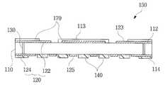
마지막으로 도 11에 도시된 바와 같이, 기판 몸체 하부면(114)에 하부 배선층(124)을 보호하는 솔더 레지스트 층(140)을 형성함으로써, 본 실시예에 따른 인쇄회로기판(150)의 제조 공정이 완료된다. 즉, 기판 몸체의 하부면(114)에 소정의 두께로 포토 솔더 레지스트를 코팅한 후에 하부 배선층의 볼 패드(125)가 노출될 수 있도록 패터닝하여 솔더 레지스트 층(140)을 형성한다.Finally, as shown in FIG. 11, the process of manufacturing the printed
이때 상부 배선층(122)의 보호층으로 사용된 프리프레그 층(170) 대신에 하 부 배선층(124)의 보호층으로 솔더 레지스트 층(140)을 형성한 이유를 설명하면, 먼저 종래와 같이 상부 배선층의 보호층으로 형성된 솔더 레지스트 층에 비해서, 하부 배선층(124)의 보호층으로 형성된 솔더 레지스트 층(140)은 흡습이나 계면 박리와 같은 문제에 대해서 자유롭다. 그리고 하부 배선층(124) 중 볼 패드들(125)을 각기 인쇄회로기판(150)의 하부면으로 노출시켜야 하는데, 프리프레그 시트는 열압착으로 형성하기 때문에, 볼 패드가 각기 노출될 수 있는 크기의 윈도우를 각각 형성하는 것이 현실적으로 어려운 점이 있다. 하지만 솔더 레지스트 층(170)은 패터닝을 통하여 형성되기 때문에, 미세한 가공이 가능하여 각각의 볼 패드들(125)을 각기 인쇄회로기판(150)의 하부면으로 노출시키는 것이 가능하다. 따라서 하부 배선층(124)의 보호층으로 솔더 레지스트 층(140)을 사용한 것이다.In this case, the reason why the solder resist
이때 본 고안의 실시예에서는 기판 몸체 하부면(114)에 형성된 볼 패드(125) 전체가 노출될 수 있도록 솔더 레지스트 층(140)이 형성된 예를 개시하였지만, 볼 패드의 중심 부분만이 노출되도록 솔더 레지스트 층을 형성할 수도 있다. 이때 전자를 NSMD(Non Solder Mask Defined)형 인쇄회로기판이라 하고, 후자를 SND(Solder Mask Defined)형 인쇄회로기판이라고 한다.In this embodiment, the solder resist
이와 같은 구조를 갖는 인쇄회로기판(150)을 이용한 반도체 패키지(200)가, 도 12 및 도 13에 도시되어 있다. 도 12 및 도 13을 참조하면, 본 발명의 실시예에 따른 반도체 패키지(200)는 인쇄회로기판(150) 상부면에 반도체 칩(161)이 실장되고, 인쇄회로기판(150) 하부면에 솔더 볼(166)이 형성된 BGA 패키지의 일종으로, 인쇄회로기판 상부면의 칩 실장 영역(113)에 접착제(163)를 개재하여 반도체 칩 (161)이 부착된다. 반도체 칩의 칩 패드(162)와 인쇄회로기판(150) 상부면의 기판 패드(123)는 본딩 와이어(164)에 의해 전기적으로 연결된다. 인쇄회로기판(150) 상부면에 형성된 반도체 칩(161)과 본딩 와이어(164)는 액상의 성형 수지로 봉합하여 형성된 수지 봉합부(165)에 의해 보호된다. 그리고 인쇄회로기판(150) 하부면의 볼 패드(125)에 각기 솔더 볼(166)이 형성된다.The
이때 반도체 칩(161)은 칩 실장 영역(113)의 프리프레그 층(170)에 접착제(163)를 매개로 접착되는데, 칩 실장 영역(113)의 표면에 균일하게 요철이 형성되어 있기 때문에, 접착제(163)와 칩 실장 영역(113)의 계면 접착 면적이 확대되어 양호한 접착성을 나타낸다.At this time, the
이울러 수지 봉합부(165)와 계면을 이루는 반도체 칩(161) 외곽의 프리프레그 층(170)의 표면에도 균일하게 요철이 형성되어 있기 때문에, 수지 봉합부(165)와 프리프레그 층(170)은 양호한 접착성을 나타낸다.In addition, since the unevenness is uniformly formed on the surface of the
한편, 본 명세서와 도면에 개시된 본 발명의 실시예들은 이해를 돕기 위해 특정 예를 제시한 것에 지나지 않으며, 본 발명의 범위를 한정하고자 하는 것은 아니다. 여기에 개시된 실시예들 이외에도 본 발명의 기술적 사상에 바탕을 둔 다른 변형예들이 실시 가능하다는 것은, 본 발명이 속하는 기술분야에서 통상의 지식을 가진 자에게 자명한 것이다.On the other hand, the embodiments of the present invention disclosed in the specification and drawings are merely presented specific examples to aid understanding, and are not intended to limit the scope of the present invention. In addition to the embodiments disclosed herein, it is apparent to those skilled in the art that other modifications based on the technical idea of the present invention may be implemented.
따라서, 본 발명의 구조를 따르면 반도체 칩이 실장되는 면에 형성된 구리 배선층의 보호층으로 프리프레그 층을 열압착 방법으로 형성함으로써, 기판 몸체 상부면과 프리프레그 층 사이의 양호한 접착성과 더불어 상부 배선층과 프리프레그 층 사이의 양호한 접착성을 동시에 확보할 수 있다.Therefore, according to the structure of the present invention, by forming the prepreg layer by the thermocompression method with the protective layer of the copper wiring layer formed on the surface on which the semiconductor chip is mounted, the upper wiring layer and the upper wiring layer together with good adhesion between the upper surface of the substrate body and the prepreg layer Good adhesion between the prepreg layers can be ensured at the same time.
동박을 열압착하여 형성한 프리프레그 층의 표면에는 균일하게 요철이 형성되기 때문에, 인쇄회로기판의 상부면에 반도체 칩을 부착할 때 사용되는 접착제와 프리프레그 층 사이의 접착 면적이 증가하여 양호한 접착성을 확보할 수 있다. 그리고 프리프레그 층과 수지 봉합부 사이의 접착 면적도 증가하기 때문에, 프리프레그 층과 수지 봉합부 사이의 양호한 계면 접착성을 확보할 수 있다.Since irregularities are uniformly formed on the surface of the prepreg layer formed by thermocompression bonding copper foil, the adhesion area between the adhesive used when attaching the semiconductor chip to the upper surface of the printed circuit board and the prepreg layer increases, resulting in good adhesion. The castle can be secured. And since the adhesive area between a prepreg layer and a resin sealing part also increases, the favorable interface adhesiveness between a prepreg layer and a resin sealing part can be ensured.
프리프레그 층은 수분을 거의 흡수하지 않는 특성을 갖고 있기 때문에, 반도체 칩과 인쇄회로기판의 계면에서 흡습에 따른 박리나 크랙의 발생을 억제할 수 있다.Since the prepreg layer has a property of hardly absorbing moisture, peeling or cracking due to moisture absorption can be suppressed at the interface between the semiconductor chip and the printed circuit board.
그리고 종래의 포토 솔더 레지스트를 대신할 보호층의 소재로 기존의 인쇄회로기판 소재로 사용되는 프리프레그를 사용함으로써, 새로운 소재 개발에 따른 비용 부담을 덜 수 있는 장점도 있다.In addition, by using a prepreg used as a conventional printed circuit board material as a material of a protective layer to replace the conventional photo solder resist, there is an advantage that can reduce the cost of developing a new material.
Claims (15)
Translated fromKoreanPriority Applications (2)
| Application Number | Priority Date | Filing Date | Title |
|---|---|---|---|
| KR1020040108782AKR100608610B1 (en) | 2004-12-20 | 2004-12-20 | Printed circuit board, manufacturing method thereof and semiconductor package using same |
| US11/145,999US20060131067A1 (en) | 2004-12-20 | 2005-06-07 | PCB, manufacturing method thereof and semiconductor package implementing the same |
Applications Claiming Priority (1)
| Application Number | Priority Date | Filing Date | Title |
|---|---|---|---|
| KR1020040108782AKR100608610B1 (en) | 2004-12-20 | 2004-12-20 | Printed circuit board, manufacturing method thereof and semiconductor package using same |
Publications (2)
| Publication Number | Publication Date |
|---|---|
| KR20060070139A KR20060070139A (en) | 2006-06-23 |
| KR100608610B1true KR100608610B1 (en) | 2006-08-08 |
Family
ID=36594272
Family Applications (1)
| Application Number | Title | Priority Date | Filing Date |
|---|---|---|---|
| KR1020040108782AExpired - Fee RelatedKR100608610B1 (en) | 2004-12-20 | 2004-12-20 | Printed circuit board, manufacturing method thereof and semiconductor package using same |
Country Status (2)
| Country | Link |
|---|---|
| US (1) | US20060131067A1 (en) |
| KR (1) | KR100608610B1 (en) |
Cited By (2)
| Publication number | Priority date | Publication date | Assignee | Title |
|---|---|---|---|---|
| WO2013032277A3 (en)* | 2011-09-02 | 2013-04-25 | Lg Innotek Co., Ltd. | Method of manufacturing substrate for chip packages and method of manufacturing chip package |
| KR101897102B1 (en)* | 2012-03-20 | 2018-10-22 | 엘지이노텍 주식회사 | Manufacturing method of chip package member for smart ic and manufacturing method of chip package |
Families Citing this family (8)
| Publication number | Priority date | Publication date | Assignee | Title |
|---|---|---|---|---|
| DE102007009371A1 (en) | 2007-02-23 | 2008-08-28 | Qimonda Ag | Semiconductor chip mounting method, involves partially or completely soaking capillary meshing on substrate e.g. printed circuit board, using thin liquid adhesive, and fitting chips to capillary meshing |
| US7919851B2 (en)* | 2008-06-05 | 2011-04-05 | Powertech Technology Inc. | Laminate substrate and semiconductor package utilizing the substrate |
| TW201104819A (en)* | 2009-07-28 | 2011-02-01 | Quanta Comp Inc | Ball grid array printed circuit board, packaging structure and fabricating methid thereof |
| CN104576427A (en)* | 2013-10-29 | 2015-04-29 | 景硕科技股份有限公司 | Method for manufacturing communication chip card substrate |
| CN104616996A (en)* | 2013-11-05 | 2015-05-13 | 景硕科技股份有限公司 | Manufacturing method of chip card substrate |
| KR102214512B1 (en) | 2014-07-04 | 2021-02-09 | 삼성전자 주식회사 | Printed circuit board and semiconductor package using the same |
| KR101990148B1 (en)* | 2015-04-14 | 2019-06-19 | 에스케이하이닉스 주식회사 | Semiconductor package |
| CN105208775B (en)* | 2015-08-07 | 2018-03-06 | 深圳崇达多层线路板有限公司 | A kind of PCB design method for preventing BGA welding from connecting tin |
Citations (5)
| Publication number | Priority date | Publication date | Assignee | Title |
|---|---|---|---|---|
| JPH0233928A (en)* | 1988-07-25 | 1990-02-05 | Hitachi Ltd | Multilayer printed wiring board and its manufacturing method |
| JP2000349438A (en) | 1999-06-02 | 2000-12-15 | Sumitomo Metal Electronics Devices Inc | Manufacture of semiconductor package |
| KR20010037813A (en)* | 1999-10-20 | 2001-05-15 | 이형도 | Printed circuit board for rambus |
| JP2002076621A (en) | 2000-08-31 | 2002-03-15 | Elna Co Ltd | Multilayer circuit board and its manufacturing method |
| JP2002314243A (en) | 2001-04-11 | 2002-10-25 | Nippon Paint Co Ltd | Primer composition for multilayer printed wiring board |
Family Cites Families (6)
| Publication number | Priority date | Publication date | Assignee | Title |
|---|---|---|---|---|
| US4012832A (en)* | 1976-03-12 | 1977-03-22 | Sperry Rand Corporation | Method for non-destructive removal of semiconductor devices |
| US5253010A (en)* | 1988-05-13 | 1993-10-12 | Minolta Camera Kabushiki Kaisha | Printed circuit board |
| DE69621983T2 (en)* | 1995-04-07 | 2002-11-21 | Shinko Electric Industries Co., Ltd. | Structure and method of assembling a semiconductor chip |
| US5872051A (en)* | 1995-08-02 | 1999-02-16 | International Business Machines Corporation | Process for transferring material to semiconductor chip conductive pads using a transfer substrate |
| US5757073A (en)* | 1996-12-13 | 1998-05-26 | International Business Machines Corporation | Heatsink and package structure for wirebond chip rework and replacement |
| US20060289203A1 (en)* | 2003-05-19 | 2006-12-28 | Dai Nippon Printing Co., Ltd. | Double-sided wiring board, double sided wiring board manufacturing method, and multilayer wiring board |
- 2004
- 2004-12-20KRKR1020040108782Apatent/KR100608610B1/ennot_activeExpired - Fee Related
- 2005
- 2005-06-07USUS11/145,999patent/US20060131067A1/ennot_activeAbandoned
Patent Citations (5)
| Publication number | Priority date | Publication date | Assignee | Title |
|---|---|---|---|---|
| JPH0233928A (en)* | 1988-07-25 | 1990-02-05 | Hitachi Ltd | Multilayer printed wiring board and its manufacturing method |
| JP2000349438A (en) | 1999-06-02 | 2000-12-15 | Sumitomo Metal Electronics Devices Inc | Manufacture of semiconductor package |
| KR20010037813A (en)* | 1999-10-20 | 2001-05-15 | 이형도 | Printed circuit board for rambus |
| JP2002076621A (en) | 2000-08-31 | 2002-03-15 | Elna Co Ltd | Multilayer circuit board and its manufacturing method |
| JP2002314243A (en) | 2001-04-11 | 2002-10-25 | Nippon Paint Co Ltd | Primer composition for multilayer printed wiring board |
Cited By (3)
| Publication number | Priority date | Publication date | Assignee | Title |
|---|---|---|---|---|
| WO2013032277A3 (en)* | 2011-09-02 | 2013-04-25 | Lg Innotek Co., Ltd. | Method of manufacturing substrate for chip packages and method of manufacturing chip package |
| US9818714B2 (en) | 2011-09-02 | 2017-11-14 | Lg Innotek Co., Ltd. | Method of manufacturing substrate for chip packages and method of manufacturing chip package |
| KR101897102B1 (en)* | 2012-03-20 | 2018-10-22 | 엘지이노텍 주식회사 | Manufacturing method of chip package member for smart ic and manufacturing method of chip package |
Also Published As
| Publication number | Publication date |
|---|---|
| US20060131067A1 (en) | 2006-06-22 |
| KR20060070139A (en) | 2006-06-23 |
Similar Documents
| Publication | Publication Date | Title |
|---|---|---|
| KR100656751B1 (en) | Electronic circuit board and manufacturing method | |
| JP2981141B2 (en) | GRID ARRAY PLASTIC PACKAGE, METHOD OF MANUFACTURING THE SAME, PLASTIC LAMINATE USED FOR MANUFACTURING THE SAME, AND METHOD OF MANUFACTURING THE SAME | |
| US5990545A (en) | Chip scale ball grid array for integrated circuit package | |
| JP4361826B2 (en) | Semiconductor device | |
| US8035035B2 (en) | Multi-layer wiring board and method of manufacturing the same | |
| US8110754B2 (en) | Multi-layer wiring board and method of manufacturing the same | |
| US6985362B2 (en) | Printed circuit board and electronic package using same | |
| JP4830120B2 (en) | Electronic package and manufacturing method thereof | |
| JPH1117048A (en) | Semiconductor chip package | |
| JP2003522401A (en) | Stacked integrated circuit package | |
| KR20100009941A (en) | Semiconductor package having stepped molding compound with conductive via, method for formation of the same and stacked semiconductor package using the same | |
| JPH09199635A (en) | Multilayer film for forming circuit substrate, multilayer circuit substrate using it, and package for semiconductor device | |
| KR100608610B1 (en) | Printed circuit board, manufacturing method thereof and semiconductor package using same | |
| JP2009135391A (en) | Electronic device and method of manufacturing the same | |
| US20050266701A1 (en) | Semiconductor device, method for manufacturing the same, circuit board, and electronic equipment | |
| KR20090041756A (en) | Printed wiring board with adhesive layer and semiconductor package using same | |
| US20010010947A1 (en) | Film ball grid array (BGA) semiconductor package | |
| KR20030085449A (en) | An improved flip chip package | |
| EP1369919A1 (en) | Flip chip package | |
| JPH0342860A (en) | Flexible printed wiring board | |
| JP3684517B2 (en) | Semiconductor device | |
| JPH098222A (en) | Electronic component device with mounted semiconductor device | |
| JP3933910B2 (en) | Manufacturing method of semiconductor device and manufacturing method of laminated structure | |
| KR20070079656A (en) | Printed Circuit Board with UV Curable Coating Layer and Manufacturing Method Thereof | |
| JP2003060125A (en) | Heat radiating bga package and method for manufacturing the same |
Legal Events
| Date | Code | Title | Description |
|---|---|---|---|
| A201 | Request for examination | ||
| PA0109 | Patent application | St.27 status event code:A-0-1-A10-A12-nap-PA0109 | |
| PA0201 | Request for examination | St.27 status event code:A-1-2-D10-D11-exm-PA0201 | |
| PN2301 | Change of applicant | St.27 status event code:A-3-3-R10-R13-asn-PN2301 St.27 status event code:A-3-3-R10-R11-asn-PN2301 | |
| PN2301 | Change of applicant | St.27 status event code:A-3-3-R10-R13-asn-PN2301 St.27 status event code:A-3-3-R10-R11-asn-PN2301 | |
| R17-X000 | Change to representative recorded | St.27 status event code:A-3-3-R10-R17-oth-X000 | |
| D13-X000 | Search requested | St.27 status event code:A-1-2-D10-D13-srh-X000 | |
| D14-X000 | Search report completed | St.27 status event code:A-1-2-D10-D14-srh-X000 | |
| PG1501 | Laying open of application | St.27 status event code:A-1-1-Q10-Q12-nap-PG1501 | |
| E701 | Decision to grant or registration of patent right | ||
| PE0701 | Decision of registration | St.27 status event code:A-1-2-D10-D22-exm-PE0701 | |
| GRNT | Written decision to grant | ||
| PR0701 | Registration of establishment | St.27 status event code:A-2-4-F10-F11-exm-PR0701 | |
| PR1002 | Payment of registration fee | St.27 status event code:A-2-2-U10-U11-oth-PR1002 Fee payment year number:1 | |
| PG1601 | Publication of registration | St.27 status event code:A-4-4-Q10-Q13-nap-PG1601 | |
| FPAY | Annual fee payment | Payment date:20090714 Year of fee payment:4 | |
| PR1001 | Payment of annual fee | St.27 status event code:A-4-4-U10-U11-oth-PR1001 Fee payment year number:4 | |
| LAPS | Lapse due to unpaid annual fee | ||
| PC1903 | Unpaid annual fee | St.27 status event code:A-4-4-U10-U13-oth-PC1903 Not in force date:20100728 Payment event data comment text:Termination Category : DEFAULT_OF_REGISTRATION_FEE | |
| PC1903 | Unpaid annual fee | St.27 status event code:N-4-6-H10-H13-oth-PC1903 Ip right cessation event data comment text:Termination Category : DEFAULT_OF_REGISTRATION_FEE Not in force date:20100728 | |
| R18-X000 | Changes to party contact information recorded | St.27 status event code:A-5-5-R10-R18-oth-X000 |