KR100607756B1 - Tungsten contact electrode manufacturing method of semiconductor device - Google Patents
Tungsten contact electrode manufacturing method of semiconductor deviceDownload PDFInfo
- Publication number
- KR100607756B1 KR100607756B1KR1020040065465AKR20040065465AKR100607756B1KR 100607756 B1KR100607756 B1KR 100607756B1KR 1020040065465 AKR1020040065465 AKR 1020040065465AKR 20040065465 AKR20040065465 AKR 20040065465AKR 100607756 B1KR100607756 B1KR 100607756B1
- Authority
- KR
- South Korea
- Prior art keywords
- tungsten
- titanium nitride
- barrier metal
- contact hole
- film
- Prior art date
- Legal status (The legal status is an assumption and is not a legal conclusion. Google has not performed a legal analysis and makes no representation as to the accuracy of the status listed.)
- Expired - Fee Related
Links
Images


Classifications
- H—ELECTRICITY
- H01—ELECTRIC ELEMENTS
- H01L—SEMICONDUCTOR DEVICES NOT COVERED BY CLASS H10
- H01L21/00—Processes or apparatus adapted for the manufacture or treatment of semiconductor or solid state devices or of parts thereof
- H01L21/02—Manufacture or treatment of semiconductor devices or of parts thereof
- H01L21/04—Manufacture or treatment of semiconductor devices or of parts thereof the devices having potential barriers, e.g. a PN junction, depletion layer or carrier concentration layer
- H01L21/18—Manufacture or treatment of semiconductor devices or of parts thereof the devices having potential barriers, e.g. a PN junction, depletion layer or carrier concentration layer the devices having semiconductor bodies comprising elements of Group IV of the Periodic Table or AIIIBV compounds with or without impurities, e.g. doping materials
- H01L21/28—Manufacture of electrodes on semiconductor bodies using processes or apparatus not provided for in groups H01L21/20 - H01L21/268
- H01L21/283—Deposition of conductive or insulating materials for electrodes conducting electric current
- H01L21/285—Deposition of conductive or insulating materials for electrodes conducting electric current from a gas or vapour, e.g. condensation
- H01L21/28506—Deposition of conductive or insulating materials for electrodes conducting electric current from a gas or vapour, e.g. condensation of conductive layers
- H01L21/28512—Deposition of conductive or insulating materials for electrodes conducting electric current from a gas or vapour, e.g. condensation of conductive layers on semiconductor bodies comprising elements of Group IV of the Periodic Table
- H01L21/2855—Deposition of conductive or insulating materials for electrodes conducting electric current from a gas or vapour, e.g. condensation of conductive layers on semiconductor bodies comprising elements of Group IV of the Periodic Table by physical means, e.g. sputtering, evaporation
- H—ELECTRICITY
- H01—ELECTRIC ELEMENTS
- H01L—SEMICONDUCTOR DEVICES NOT COVERED BY CLASS H10
- H01L21/00—Processes or apparatus adapted for the manufacture or treatment of semiconductor or solid state devices or of parts thereof
- H01L21/70—Manufacture or treatment of devices consisting of a plurality of solid state components formed in or on a common substrate or of parts thereof; Manufacture of integrated circuit devices or of parts thereof
- H01L21/71—Manufacture of specific parts of devices defined in group H01L21/70
- H01L21/768—Applying interconnections to be used for carrying current between separate components within a device comprising conductors and dielectrics
- H01L21/76801—Applying interconnections to be used for carrying current between separate components within a device comprising conductors and dielectrics characterised by the formation and the after-treatment of the dielectrics, e.g. smoothing
- H01L21/76802—Applying interconnections to be used for carrying current between separate components within a device comprising conductors and dielectrics characterised by the formation and the after-treatment of the dielectrics, e.g. smoothing by forming openings in dielectrics
- H—ELECTRICITY
- H01—ELECTRIC ELEMENTS
- H01L—SEMICONDUCTOR DEVICES NOT COVERED BY CLASS H10
- H01L21/00—Processes or apparatus adapted for the manufacture or treatment of semiconductor or solid state devices or of parts thereof
- H01L21/70—Manufacture or treatment of devices consisting of a plurality of solid state components formed in or on a common substrate or of parts thereof; Manufacture of integrated circuit devices or of parts thereof
- H01L21/71—Manufacture of specific parts of devices defined in group H01L21/70
- H01L21/768—Applying interconnections to be used for carrying current between separate components within a device comprising conductors and dielectrics
- H01L21/76838—Applying interconnections to be used for carrying current between separate components within a device comprising conductors and dielectrics characterised by the formation and the after-treatment of the conductors
- H01L21/76841—Barrier, adhesion or liner layers
- H01L21/76843—Barrier, adhesion or liner layers formed in openings in a dielectric
- H—ELECTRICITY
- H01—ELECTRIC ELEMENTS
- H01L—SEMICONDUCTOR DEVICES NOT COVERED BY CLASS H10
- H01L21/00—Processes or apparatus adapted for the manufacture or treatment of semiconductor or solid state devices or of parts thereof
- H01L21/70—Manufacture or treatment of devices consisting of a plurality of solid state components formed in or on a common substrate or of parts thereof; Manufacture of integrated circuit devices or of parts thereof
- H01L21/71—Manufacture of specific parts of devices defined in group H01L21/70
- H01L21/768—Applying interconnections to be used for carrying current between separate components within a device comprising conductors and dielectrics
- H01L21/76838—Applying interconnections to be used for carrying current between separate components within a device comprising conductors and dielectrics characterised by the formation and the after-treatment of the conductors
- H01L21/76877—Filling of holes, grooves or trenches, e.g. vias, with conductive material
Landscapes
- Engineering & Computer Science (AREA)
- Physics & Mathematics (AREA)
- Condensed Matter Physics & Semiconductors (AREA)
- General Physics & Mathematics (AREA)
- Manufacturing & Machinery (AREA)
- Computer Hardware Design (AREA)
- Microelectronics & Electronic Packaging (AREA)
- Power Engineering (AREA)
- Internal Circuitry In Semiconductor Integrated Circuit Devices (AREA)
Abstract
Translated fromKoreanDescription
Translated fromKorean도 1a 내지 도 1e는 종래 기술에 의한 반도체 소자의 텅스텐 콘택 전극 제조 방법을 순차적으로 나타낸 공정 순서도,1A to 1E are process flowcharts sequentially illustrating a method for manufacturing a tungsten contact electrode of a semiconductor device according to the prior art;
도 2는 종래 기술에 의한 콘택 전극의 텅스텐 증착 과정을 나타낸 흐름도,2 is a flowchart illustrating a tungsten deposition process of a contact electrode according to the prior art;
도 3a 내지 도 3e는 본 발명에 따른 반도체 소자의 텅스텐 콘택 전극 제조 방법을 순차적으로 나타낸 공정 순서도,3A to 3E are process flowcharts sequentially illustrating a method of manufacturing a tungsten contact electrode of a semiconductor device according to the present invention;
도 4는 본 발명에 따른 콘택 전극의 텅스텐 증착 과정을 나타낸 흐름도.4 is a flowchart illustrating a tungsten deposition process of a contact electrode according to the present invention.
본 발명은 반도체 소자의 제조 방법에 관한 것으로서, 특히 텅스텐 콘택(contact) 전극을 형성할 때 콘택 전극내 빈 공간(void) 생성을 미연에 방지할 수 있는 반도체 소자의 텅스텐 콘택 전극 제조 방법에 관한 것이다.BACKGROUND OF THE INVENTION 1. Field of the Invention The present invention relates to a method for manufacturing a semiconductor device, and more particularly, to a method for manufacturing a tungsten contact electrode of a semiconductor device capable of preventing generation of voids in a contact electrode when forming a tungsten contact electrode. .
현재 반도체 소자가 고집적화에 따라 디자인 룰이 감소되고 이에 따라 반도체 소자의 배선 사이 또는 기판과 배선을 수직으로 연결하는 콘택 전극의 면적이 축소되는 추세이다. 따라서 반도체 소자의 고집적화에 따른 미세한 콘택 전극은 반도체 소자의 제조 공정에 있어서 매우 중요하다.As the semiconductor devices are highly integrated, design rules are reduced, and accordingly, the area of contact electrodes that vertically connect the wirings of the semiconductor devices or between the substrates and the wirings is reduced. Therefore, the fine contact electrode according to the high integration of the semiconductor device is very important in the manufacturing process of the semiconductor device.
도 1a 내지 도 1e는 종래 기술에 의한 반도체 소자의 텅스텐 콘택 전극 제조 방법을 순차적으로 나타낸 공정 순서도로서, 이들 도면들을 참조하여 종래 반도체 배선 사이를 수직으로 연결하기 위한 텅스텐 콘택 전극의 제조 과정에 대해 설명한다.1A through 1E are process flowcharts sequentially illustrating a method of manufacturing a tungsten contact electrode of a semiconductor device according to the prior art, and a process of manufacturing a tungsten contact electrode for vertically connecting conventional semiconductor wires will be described with reference to these drawings. do.
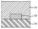
우선 도 1a에 도시된 바와 같이, 반도체 기판으로서 실리콘 기판에 반도체 소자, 예를 들어 MOSFET 제조 공정을 실시한다. 그리고 그 위에 층간 절연막(10)을 형성하고 층간 절연막(10) 상부에 하부 MOSFET와 수직으로 연결되기 위한 하부 금속 배선(12)을 형성한다. 이때 층간 절연막(10)은 BPSG(Boro Pospho Silicate Glass), PSG(Pospho Silicate Glass), BSG(Boro Silicate Glass), HDP(High Density Plasma) 산화막 등의 절연 물질로 형성하고, 하부 금속 배선(12)은 알루미늄 등의 금속 물질, 이의 합금 물질 등으로 형성한다. 그리고 층간 절연막(10) 상부에 다시 층간 절연막(14), 예를 들어 HDP 산화막으로 증착하고, 그 표면을 화학기계적연마(CMP : Chemical Mechanical Polishing) 공정으로 평탄화한다.First, as shown in FIG. 1A, a semiconductor device, for example, a MOSFET manufacturing process is performed on a silicon substrate as a semiconductor substrate. An
도 1b에 도시된 바와 같이, 층간 절연막(14) 상부에 포토레지스트를 도포하고 콘택홀 영역을 정의하는 마스크로 포토레지스트를 노광한 후에 이를 현상함으로써 포토레지스트 패턴(16)을 형성한다. 계속해서 포토레지스트 패턴(16)에 의해 드러난 층간 절연막(14)을 건식 식각 공정으로 식각하여 하부 금속 배선(12)이 노출되는 콘택홀(18)을 형성한 후에 에슁(ashing) 공정으로 포토레지스트 패턴(16)을 제거한다.As shown in FIG. 1B, the photoresist pattern 16 is formed by applying a photoresist on the
도 1c에 도시된 바와 같이, 콘택홀이 형성된 층간 절연막(14) 상부에 장벽 금속막(barrier metal)(20)으로서 티타늄(Ti) 및 티타늄질화막(TiN)을 순차적으로 적층하여 형성한다. 이때 장벽 금속막(20)은 물리기상증착(PVD : Physical Vapor Deposition) 공정 또는 화학기상증착(CVD : Chemical Vapor Deposition) 공정으로 진행될 수 있으나 대개 PVD인 스퍼터링(sputtering) 방식으로 증착된다. 예를 들어, 티타늄(Ti)의 두께를 200Å∼500Å, 티타늄질화막(TiN)의 두께를 100Å∼500Å으로 한다.As illustrated in FIG. 1C, titanium (Ti) and titanium nitride (TiN) are sequentially formed as a
계속해서 도 1d에 도시된 바와 같이, 장벽 금속막(20)이 형성된 콘택홀에 도전체 물질로서 텅스텐(W)(22)을 화학기상증착(CVD) 공정으로 약 3000Å∼7000Å 두께로 증착하여 콘택홀을 완전히 갭필(gap-fill)한다. 이에 대한 텅스텐 갭필 공정은 도 2를 참조하여 추후에 보다 상세하게 설명한다.Subsequently, as shown in FIG. 1D, the contact is formed by depositing tungsten (W) 22 as a conductive material in a chemical vapor deposition (CVD) process to a thickness of about 3000 kPa to 7000 kPa in the contact hole where the
그리고나서 도 1e에 도시된 바와 같이, 화학기계적연마(CMP) 공정으로 텅스텐(W) 및 장벽 금속막(20)을 층간 절연막(14) 표면이 드러날 때까지 평탄화하여 장벽 금속막(20)에 의해 하부 금속 배선(12)과 수직으로 연결되며 표면이 평탄화된 텅스텐 콘택 전극(22')을 형성한다.Then, as shown in FIG. 1E, the tungsten (W) and the
그런데 종래 기술에 의한 콘택홀의 텅스텐(22) 증착 공정은 대개 화학기상증착(CVD) 공정으로 진행하는데, 대개 도 2와 같이 텅스텐 증착 전 공정과 텅스텐 증착 공정으로 구분된다.However, the tungsten (22) deposition process of the contact hole according to the prior art generally proceeds to a chemical vapor deposition (CVD) process, and is generally divided into a tungsten deposition process and a tungsten deposition process as shown in FIG.
예를 들어, 화학기상증착(CVD) 챔버내 압력을 설정된 압력인 90Torr 이상으로 올려주고 챔버내 온도를 380℃ 이상으로 히팅한다(S10).For example, the pressure in the chemical vapor deposition (CVD) chamber is raised to a set pressure of 90 Torr or more and the temperature in the chamber is heated to 380 ° C. or more (S10).
그리고 화학기상증착(CVD) 챔버에 사일렌(SiH4) 가스를 주입하여 사일렌 가스에 의한 소킹(soaking) 공정을 진행하여 장벽 금속막 표면에 실리콘 모노층을 형성시킨다(S12). 이때 실리콘 모노층은 이후 텅스텐 헥사플로라이트(WF6)의 플루오린(F)과 실리콘을 반응해서 장벽 금속막에 미치는 영향을 줄이는 역할을 한다.In addition, a silicon monolayer is formed on the surface of the barrier metal film by injecting a silica (SiH 4) gas into a chemical vapor deposition (CVD) chamber and performing a soaking process using the siylene gas (S12). At this time, the silicon monolayer serves to reduce the influence on the barrier metal film by reacting silicon with fluorine (F) of tungsten hexaflolite (WF6).
그 다음 화학기상증착(CVD) 챔버내 압력을 약 30Torr 정도 낮추고 수소(H), 사일렌(SiH4)의 가스를 주입하면서 텅스텐 헥사플로라이드(WF6) 가스를 소량(예를 들어 50sccm) 주입하여 수소(H), 사일렌(SiH4) 및 텅스텐 헥사플로라이트(WF6)의 반응으로 텅스텐 핵을 생성한다(S14). 이때 텅스텐 핵의 생성 두께는 예를 들어 500Å이하로 형성될 수 있으며 이는 콘택 전극의 프로파일에 따라 그 두께를 다르게 할 수 있다.Then, lower the pressure in the chemical vapor deposition (CVD) chamber by about 30 Torr and inject a small amount of tungsten hexafluoride (WF6) gas (for example, 50 sccm) while injecting hydrogen (H) and xylene (SiH4) gas. Tungsten nuclei are generated by the reaction of (H), xylene (SiH 4) and tungsten hexaflolite (WF 6) (S14). At this time, the production thickness of the tungsten nucleus may be formed, for example, 500 Å or less, which may vary the thickness according to the profile of the contact electrode.
계속해서 화학기상증착(CVD) 챔버내 압력을 다시 설정된 90Torr 이상으로 올려준다(S16).Subsequently, the pressure in the chemical vapor deposition (CVD) chamber is raised to above 90 Torr (S16).
그리고 나서 화학기상증착(CVD) 챔버에 사일렌(SiH4) 가스의 주입을 차단하고 수소(H) 가스를 주입하고 텅스텐 헥사플로라이트(WF6) 가스를 다량(예를 들어 90sccm) 주입하여 수소(H) 및 텅스텐 헥사플로라이트(WF6)의 반응으로 텅스텐(W)을 증착함으로써 콘택홀 내부를 텅스텐(W)으로 완전히 갭필한다(S18).Then, the injection of the silicide (SiH4) gas into the chemical vapor deposition (CVD) chamber is blocked, the hydrogen (H) gas is injected, and a large amount (for example, 90 sccm) of tungsten hexaflorite (WF6) gas is injected to the hydrogen (H). And depositing tungsten (W) by the reaction of tungsten hexaflolite (WF6) to completely fill the contact hole with tungsten (W) (S18).
그런데 이와 같은 종래 기술에 의해 콘택홀 내부를 갭필하는 텅스텐(W)을 화학기상증착(CVD) 공정으로 증착할 경우 텅스텐 헥사플로라이트(WF6)에 함유되어 있는 플루오린(F)이 실리콘 모노층의 실리콘과 반응하는 사일렌(SiH4) 가스에 의한 소킹 공정에 의해 완전히 제거되지 않고 장벽 금속막의 티타늄(Ti)과 반응하게 된 다. 이에 따라 콘택홀에 반응 생성물(TiF3, TiF4, SiFx 및 WSix 등)이 형성되어 콘택 전극의 콘택 저항을 증가시키거나 후속 열공정시 팽창해서 콘택 전극이 오픈되는 등의 문제점을 야기시키게 된다.However, in the case of depositing tungsten (W) which gap-fills the inside of a contact hole by a chemical vapor deposition (CVD) process according to the related art, fluorine (F) contained in tungsten hexaflolite (WF6) is silicon of a silicon monolayer. It is not completely removed by the soaking process using a silylene (SiH 4) gas which reacts with the titanium oxide, and reacts with titanium (Ti) of the barrier metal film. As a result, reaction products (TiF3, TiF4, SiFx, WSix, etc.) are formed in the contact holes, which causes problems such as increasing the contact resistance of the contact electrodes or expanding during the subsequent thermal process to open the contact electrodes.
또한 종래 기술에 의한 반도체 소자의 콘택 전극 제조 방법은 반도체 소자의 고집적화에 따른 스텝커버리지(step coverage)가 큰 콘택홀 내에 도 2와 같은 화학기상증착(CVD)법으로 텅스텐(W)을 증착할 경우 텅스텐이 완전히 갭필되지 못하고 빈 공간이 형성되어 콘택 전극의 전기적 특성 및 신뢰성을 저하시키는 문제점이 있었다.In addition, according to the related art, a method of manufacturing a contact electrode of a semiconductor device is obtained by depositing tungsten (W) in a chemical vapor deposition (CVD) method as shown in FIG. 2 in a contact hole having large step coverage due to high integration of a semiconductor device. Tungsten is not completely gapfilled and an empty space is formed, thereby degrading electrical characteristics and reliability of the contact electrode.
본 발명의 목적은 상기와 같은 종래 기술의 문제점을 해결하기 위하여 콘택홀에 텅스텐(W)을 화학기상증착법으로 증착할 때 사일렌(SiH4) 가스에 의한 소킹 공정 이전에 질소(N2) 가스에 의한 소킹 공정을 진행하여 티타늄질화막(TiN)의 표면을 활성화시켜 텅스텐 헥사플로라이트(WF6)의 플루오린(F)이 티타늄으로 침투되는 것을 막으면서 텅스텐의 갭필 능력을 향상시킬 수 있는 반도체 소자의 텅스텐 콘택 전극 제조 방법을 제공하는데 있다.An object of the present invention is to solve the problems of the prior art as described above by the nitrogen (N2) gas before the soaking process by using a silica (SiH4) gas when depositing tungsten (W) in the chemical vapor deposition method in the contact hole Tungsten contact electrode of a semiconductor device capable of improving the gap fill capability of tungsten while preventing the penetration of fluorine (F) of tungsten hexaflolite (WF6) into titanium by activating the surface of the titanium nitride film (TiN) by performing a soaking process. It is to provide a manufacturing method.
상기 목적을 달성하기 위하여 본 발명은 반도체 기판의 층간 절연막에 콘택홀을 형성하고 콘택홀이 형성된 층간 절연막 상부에 티타늄막과 티타늄 질화막이 적층된 장벽 금속막을 형성하고, 장벽 금속막이 형성된 반도체 기판에 텅스텐을 증착하여 콘택홀을 갭필하는 반도체 소자의 텅스텐 콘택 전극 제조 방법에 있어서, 텅스텐 증착에 의해 콘택홀을 갭필하는 단계는, 장벽 금속막을 질소 가스에 의해 소킹하여 티타늄 질화막 표면을 활성화시키는 단계와, 활성화된 티타늄 질화막을 사일렌 가스에 의해 소킹하여 티타늄 질화막 표면에 실리콘 모노층을 형성하는 단계와, 장벽 금속막 상부에 텅스텐 핵을 형성하는 단계와, 텅스텐 핵이 형성된 반도체 기판에 텅스텐을 증착하여 콘택홀을 갭필하는 단계를 포함한다.In order to achieve the above object, the present invention forms a contact hole in the interlayer insulating film of the semiconductor substrate and forms a barrier metal film in which a titanium film and a titanium nitride film are stacked on the interlayer insulating film on which the contact hole is formed, and a tungsten on the semiconductor substrate on which the barrier metal film is formed. In the method for manufacturing a tungsten contact electrode of a semiconductor device, which deposits a gap and fills a contact hole, the step of gapfilling a contact hole by tungsten deposition may include: activating a titanium nitride film surface by soaking a barrier metal film with nitrogen gas; Soaking the titanium nitride film with a xylene gas to form a silicon monolayer on the surface of the titanium nitride film, forming a tungsten nucleus on the barrier metal film, and depositing tungsten on the semiconductor substrate on which the tungsten nucleus is formed. Gap-filling.
이하 첨부된 도면을 참조하여 본 발명의 바람직한 실시예에 대해 설명하고자 한다.Hereinafter, exemplary embodiments of the present invention will be described with reference to the accompanying drawings.
도 3a 내지 도 3e는 본 발명에 따른 반도체 소자의 텅스텐 콘택 전극 제조 방법을 순차적으로 나타낸 공정 순서도이다. 이들 도면을 참조하면 본 발명의 일 실시예에 따른 텅스텐 콘택 전극 제조 방법을 설명하면 다음과 같다.3A to 3E are process flowcharts sequentially illustrating a method of manufacturing a tungsten contact electrode of a semiconductor device according to the present invention. Referring to these drawings, a tungsten contact electrode manufacturing method according to an embodiment of the present invention will be described.
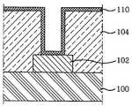
우선 도 3a에 도시된 바와 같이, 반도체 기판으로서 실리콘 기판에 반도체 소자, 예를 들어 MOSFET 제조 공정을 실시한다. 그리고 그 위에 BPSG, PSG, BSG, HDP 산화막 등의 절연 물질로 층간 절연막(100)을 형성하고 층간 절연막(100) 상부에 하부 MOSFET와 수직으로 연결하기 위한 하부 금속 배선(102)을 형성한다. 이때 하부 금속 배선(102)은 알루미늄 등의 금속 물질, 이의 합금 물질로 형성한다. 그리고 층간 절연막(100) 상부에 다시 층간 절연막(104), 예를 들어 HDP 산화막으로 증착하고, 그 표면을 화학기계적연마(CMP) 공정으로 평탄화한다.First, as shown in FIG. 3A, a semiconductor device, for example, a MOSFET manufacturing process is performed on a silicon substrate as a semiconductor substrate. An
계속해서 도 3b에 도시된 바와 같이, 평탄화된 층간 절연막(104) 상부에 포토레지스트를 도포하고 콘택홀 영역을 정의하는 마스크로 포토레지스트를 노광한 후에 이를 현상함으로써 포토레지스트 패턴(106)을 형성한다. 이어서 포토레지스 트 패턴(106)에 의해 드러난 층간 절연막(104)을 건식 식각 공정으로 식각하여 하부 금속 배선(102)이 노출되는 콘택홀(108)을 형성한 후에 에슁 공정으로 포토레지스트 패턴(106)을 제거한다.Subsequently, as shown in FIG. 3B, the
도 3c에 도시된 바와 같이, 콘택홀이 형성된 층간 절연막(104) 상부에 장벽 금속막(110)으로서 티타늄(Ti) 및 티타늄질화막(TiN)을 순차적으로 형성한다. 이때 장벽 금속막(110)은 물리기상증착(PVD) 또는 화학기상증착(CVD) 공정으로 증착하고, 예를 들어 티타늄(Ti)의 두께를 200Å∼500Å, 티타늄질화막(TiN)의 두께를 100Å∼500Å으로 증착한다. 만약 물리기상증착(PVD) 공정 중에서 플라즈마 방식으로 장벽 금속막(110)을 형성할 경우 챔버 안에 아르곤(Ar)을 넣어주며 DC 전원을 걸어주고 티타늄 소스를 주입함으로써 플라즈마에 의해 티타늄(Ti)을 증착한 후에, 티타늄질화막(TiN)의 소스인 TDMAT(또는 TiCl4)을 챔버 안에 주입하면 플라즈마에 의하 티타늄질화막(TiN)을 증착하게 된다.As shown in FIG. 3C, titanium (Ti) and titanium nitride (TiN) are sequentially formed as the
이어서 도 3d에 도시된 바와 같이, 장벽 금속막(110)이 형성된 콘택홀에 도전체 물질로서 텅스텐(W)(112)을 본 발명의 화학기상증착(CVD) 공정 조건에 따라 약 3000Å∼7000Å 두께로 증착하여 콘택홀을 완전히 갭필한다. 이에 대한 텅스텐 화학기상증착 공정은 추후에 보다 상세하게 설명한다.As shown in FIG. 3D, tungsten (W) 112 is used as a conductive material in the contact hole in which the
그리고나서 도 3e에 도시된 바와 같이, 화학기계적연마(CMP) 공정으로 텅스텐(W) 및 장벽 금속막(110)을 층간 절연막(104) 표면이 드러날 때까지 평탄화하여 장벽 금속막(110)에 의해 하부 금속 배선(102)과 수직으로 연결되며 표면이 평탄화된 텅스텐 콘택 전극(112')을 형성한다.Then, as shown in FIG. 3E, the tungsten (W) and the
상술한 본 발명에 따른 콘택홀의 텅스텐 화학기상증착(CVD) 공정은 도 4를 참조하여 설명하고자 한다.The above-described tungsten chemical vapor deposition (CVD) process of the contact hole according to the present invention will be described with reference to FIG. 4.
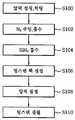
우선, 화학기상증착(CVD) 챔버내 압력을 설정된 압력인 90Torr 이상으로 올려주고 챔버내 온도를 380℃ 이상으로 히팅한다(S100).First, the pressure in the chemical vapor deposition (CVD) chamber is raised to a set pressure of 90 Torr or more and the temperature in the chamber is heated to 380 ° C. or more (S100).
그리고 화학기상증착(CVD) 챔버내 온도를 380℃ 이상으로 계속 유지하고 챔버 압력을 10Torr 이상으로 설정한 상태에서 질소(N2) 가스를 공급하여 질소 가스에 의한 소킹 공정을 진행함으로써 장벽 금속막의 티타늄 질화막(TiN) 표면이 질소 이온과의 반응 및 확산하여 활성화된다(S102). 이때 질소(N2) 가스에 의한 소킹 공정은 30초이상 진행하는 것이 바람직하다.The titanium nitride film of the barrier metal film is subjected to a soaking process by supplying nitrogen (N2) gas while maintaining the temperature in the chemical vapor deposition (CVD) chamber at 380 ° C or higher and setting the chamber pressure to 10 Torr or higher. The (TiN) surface is activated by reaction and diffusion with nitrogen ions (S102). At this time, the soaking process by nitrogen (N2) gas is preferably proceed for 30 seconds or more.
그 다음 화학기상증착(CVD) 챔버에 사일렌(SiH4) 가스를 공급하여 사일렌(SiH4) 가스에 의한 소킹 공정을 진행하여 장벽 금속막 표면에 실리콘 모노층을 형성시킨다(S104). 이때 실리콘 모노층은 이후 텅스텐 헥사플로라이트(WF6)의 플루오린(F)과 실리콘을 반응해서 장벽 금속막에 미치는 영향을 줄이는 역할을 한다.Next, a silicon monolayer is formed on the surface of the barrier metal film by supplying a silica (SiH 4) gas to a chemical vapor deposition (CVD) chamber and proceeding a soaking process using a silica (SiH 4) gas (S104). At this time, the silicon monolayer serves to reduce the influence on the barrier metal film by reacting silicon with fluorine (F) of tungsten hexaflolite (WF6).
그 다음 화학기상증착(CVD) 챔버내 압력을 약 30Torr 정도로 낮추고 수소(H), 사일렌(SiH4)의 가스를 주입하면서 텅스텐 헥사플로라이드(WF6) 가스를 소량, 예를 들어 50sccm 이하로 주입하여 수소(H), 사일렌(SiH4) 및 텅스텐 헥사플로라이트(WF6)의 화학적 반응으로 텅스텐 핵을 생성한다(S106). 이때 텅스텐 핵의 생성 두께는 예를 들어 500Å이하로 형성될 수 있으며 이는 콘택 전극의 프로파일에 따라 그 두께를 다르게 할 수 있다.Then, the pressure in the chemical vapor deposition (CVD) chamber was lowered to about 30 Torr, and a small amount of tungsten hexafluoride (WF6) gas was injected, for example, 50 sccm or less while injecting hydrogen (H) and xylene (SiH4) gas. Tungsten nuclei are generated by chemical reaction of hydrogen (H), xylene (SiH 4) and tungsten hexaflolite (WF 6) (S106). At this time, the production thickness of the tungsten nucleus may be formed, for example, 500 Å or less, which may vary the thickness according to the profile of the contact electrode.
계속해서 화학기상증착(CVD) 챔버내 압력을 다시 설정된 90Torr 이상으로 올 려준다(S108).Subsequently, the pressure in the chemical vapor deposition (CVD) chamber is increased again to a set value of 90 Torr or more (S108).
그리고나서 화학기상증착(CVD) 챔버에 사일렌(SiH4) 가스의 주입을 차단하고 수소(H) 가스를 주입하고 텅스텐 헥사플로라이트(WF6) 가스를 다량, 예를 들어 90sccm 이상으로 주입하여 수소(H) 및 텅스텐 헥사플로라이트(WF6)의 화학적 반응으로 텅스텐(W)을 증착함으로써 콘택홀 내부를 텅스텐(W)으로 완전히 갭필한다(S110).Then, the injection of the SiH4 gas into the chemical vapor deposition (CVD) chamber is blocked, the hydrogen (H) gas is injected, and the tungsten hexaflorite (WF6) gas is injected at a large amount, for example, 90 sccm or more, to inject hydrogen (H). ) And tungsten (W) by chemical reaction of tungsten hexaflolite (WF6) to completely gapfill the inside of the contact hole with tungsten (W) (S110).
따라서 본 발명에 따라 콘택홀 내부를 갭필하는 텅스텐(W)을 화학기상증착(CVD) 공정으로 증착할 경우 사일렌(SiH4) 가스에 의한 소킹 공정 이전에 질소(N2) 가스에 의한 소킹 공정을 진행하여 장벽 금속막의 티타늄 질화막(TiN)을 활성화함으로써 이후 텅스텐 증착시 텅스텐 헥사플로라이트(WF6)에 함유되어 있는 플루오린(F)이 장벽 금속막의 티타늄(Ti)과 반응하는 것을 효과적으로 차단할 수 있다.Therefore, in the case of depositing tungsten (W) which gap-fills the inside of the contact hole by chemical vapor deposition (CVD) process, the soaking process by nitrogen (N2) gas is performed before the soaking process by siren (SiH4) gas. By activating the titanium nitride layer (TiN) of the barrier metal layer, it is possible to effectively block the reaction of fluorine (F) contained in the tungsten hexaflorite (WF6) with titanium (Ti) of the barrier metal layer during tungsten deposition.
이에 따라 콘택홀에 반응 생성물(TiF3, TiF4, SiFx 및 WSix 등)이 형성되지 않게 되어 결국 콘택 전극의 콘택 저항이 감소하게 되면서 콘택홀에서의 텅스텐 증착이 용이하게 되어 빈 공간없이 텅스텐을 완전히 갭필할 수 있다.As a result, reaction products (TiF3, TiF4, SiFx, WSix, etc.) are not formed in the contact holes, and thus the contact resistance of the contact electrodes is reduced, thereby easily depositing tungsten in the contact holes, thereby completely gapfilling tungsten without empty space. Can be.
이상 설명한 바와 같이, 본 발명은 콘택홀에 텅스텐(W)을 화학기상증착법으로 증착할 때 사일렌(SiH4) 가스에 의한 소킹 공정 이전에 질소(N2) 가스에 의한 소킹 공정을 추가함으로써 티타늄질화막(TiN)의 표면을 활성화시켜 텅스텐 헥사플로라이트(WF6)의 플루오린(F)이 티타늄으로 침투되는 것을 막으면서 콘택홀로의 텅스텐 갭필 능력을 향상시킬 수 있는 효과가 있다.As described above, the present invention provides a titanium nitride film (N2) by adding a soaking process using nitrogen (N2) gas before the soaking process by using a silicide (SiH4) gas when depositing tungsten (W) into a contact hole. By activating the surface of TiN), the fluorine (F) of tungsten hexaflolite (WF6) is prevented from penetrating into titanium, thereby improving the tungsten gapfill ability to the contact hole.
한편, 본 발명은 상술한 실시예에 국한되는 것이 아니라 후술되는 청구범위에 기재된 본 발명의 기술적 사상과 범주내에서 당업자에 의해 여러 가지 변형이 가능하다.On the other hand, the present invention is not limited to the above-described embodiment, various modifications are possible by those skilled in the art within the spirit and scope of the present invention described in the claims to be described later.
Claims (4)
Translated fromKoreanPriority Applications (1)
| Application Number | Priority Date | Filing Date | Title |
|---|---|---|---|
| KR1020040065465AKR100607756B1 (en) | 2004-08-19 | 2004-08-19 | Tungsten contact electrode manufacturing method of semiconductor device |
Applications Claiming Priority (1)
| Application Number | Priority Date | Filing Date | Title |
|---|---|---|---|
| KR1020040065465AKR100607756B1 (en) | 2004-08-19 | 2004-08-19 | Tungsten contact electrode manufacturing method of semiconductor device |
Publications (2)
| Publication Number | Publication Date |
|---|---|
| KR20060016978A KR20060016978A (en) | 2006-02-23 |
| KR100607756B1true KR100607756B1 (en) | 2006-08-01 |
Family
ID=37125122
Family Applications (1)
| Application Number | Title | Priority Date | Filing Date |
|---|---|---|---|
| KR1020040065465AExpired - Fee RelatedKR100607756B1 (en) | 2004-08-19 | 2004-08-19 | Tungsten contact electrode manufacturing method of semiconductor device |
Country Status (1)
| Country | Link |
|---|---|
| KR (1) | KR100607756B1 (en) |
Cited By (2)
| Publication number | Priority date | Publication date | Assignee | Title |
|---|---|---|---|---|
| CN103578963A (en)* | 2012-08-02 | 2014-02-12 | 中国科学院微电子研究所 | Semiconductor device and method for manufacturing the same |
| CN103794502A (en)* | 2012-10-30 | 2014-05-14 | 中国科学院微电子研究所 | Semiconductor device and method for manufacturing the same |
Families Citing this family (1)
| Publication number | Priority date | Publication date | Assignee | Title |
|---|---|---|---|---|
| WO2020131392A1 (en)* | 2018-12-20 | 2020-06-25 | Applied Materials, Inc. | Method of growing doped group iv materials |
- 2004
- 2004-08-19KRKR1020040065465Apatent/KR100607756B1/ennot_activeExpired - Fee Related
Cited By (2)
| Publication number | Priority date | Publication date | Assignee | Title |
|---|---|---|---|---|
| CN103578963A (en)* | 2012-08-02 | 2014-02-12 | 中国科学院微电子研究所 | Semiconductor device and method for manufacturing the same |
| CN103794502A (en)* | 2012-10-30 | 2014-05-14 | 中国科学院微电子研究所 | Semiconductor device and method for manufacturing the same |
Also Published As
| Publication number | Publication date |
|---|---|
| KR20060016978A (en) | 2006-02-23 |
Similar Documents
| Publication | Publication Date | Title |
|---|---|---|
| US6787461B2 (en) | Method for forming a plug metal layer | |
| US6927163B2 (en) | Method and apparatus for manufacturing a barrier layer of semiconductor device | |
| KR100599434B1 (en) | Metal wiring formation method of semiconductor device | |
| US20060246714A1 (en) | Method of forming a conductive contact | |
| US20020135071A1 (en) | Integrated circuit device contact plugs having a liner layer that exerts compressive stress thereon and methods of manufacturing same | |
| US6696368B2 (en) | Titanium boronitride layer for high aspect ratio semiconductor devices | |
| US6911382B2 (en) | Method of forming a contact in a semiconductor device utilizing a plasma treatment | |
| US5977636A (en) | Method of forming an electrically conductive contact plug, method of forming a reactive or diffusion barrier layer over a substrate, integrated circuitry, and method of forming a layer of titanium boride | |
| JP2000058650A (en) | Semiconductor device, and method and device for manufacturing the device | |
| JP3027946B2 (en) | Semiconductor device and manufacturing method thereof | |
| US7259092B2 (en) | Semiconductor device and method for fabricating the same | |
| KR100607756B1 (en) | Tungsten contact electrode manufacturing method of semiconductor device | |
| US6596629B2 (en) | Method for forming wire in semiconductor device | |
| US6048794A (en) | Selective W CVD plug process with a RTA self-aligned W-silicide barrier layer | |
| JP4052623B2 (en) | Manufacturing method of semiconductor device | |
| US20070037378A1 (en) | Method for forming metal pad in semiconductor device | |
| KR100629961B1 (en) | Metal contact formation method of semiconductor device | |
| KR100875073B1 (en) | Metal wiring formation method of semiconductor device | |
| KR100827521B1 (en) | Capacitor of semiconductor device and manufacturing method thereof | |
| JP3129251B2 (en) | Contact plug formation method | |
| KR100325597B1 (en) | Method for forming contact hole in semiconductor device | |
| KR100587594B1 (en) | Metal wiring formation method of semiconductor device | |
| KR20040060005A (en) | Method for forming barrier metal layer in semiconductor device | |
| KR20020048443A (en) | Method for fabricating semiconductor device |
Legal Events
| Date | Code | Title | Description |
|---|---|---|---|
| A201 | Request for examination | ||
| PA0109 | Patent application | St.27 status event code:A-0-1-A10-A12-nap-PA0109 | |
| PA0201 | Request for examination | St.27 status event code:A-1-2-D10-D11-exm-PA0201 | |
| R18-X000 | Changes to party contact information recorded | St.27 status event code:A-3-3-R10-R18-oth-X000 | |
| PG1501 | Laying open of application | St.27 status event code:A-1-1-Q10-Q12-nap-PG1501 | |
| E902 | Notification of reason for refusal | ||
| PE0902 | Notice of grounds for rejection | St.27 status event code:A-1-2-D10-D21-exm-PE0902 | |
| PN2301 | Change of applicant | St.27 status event code:A-3-3-R10-R13-asn-PN2301 St.27 status event code:A-3-3-R10-R11-asn-PN2301 | |
| PN2301 | Change of applicant | St.27 status event code:A-3-3-R10-R13-asn-PN2301 St.27 status event code:A-3-3-R10-R11-asn-PN2301 | |
| E13-X000 | Pre-grant limitation requested | St.27 status event code:A-2-3-E10-E13-lim-X000 | |
| P11-X000 | Amendment of application requested | St.27 status event code:A-2-2-P10-P11-nap-X000 | |
| P13-X000 | Application amended | St.27 status event code:A-2-2-P10-P13-nap-X000 | |
| E701 | Decision to grant or registration of patent right | ||
| PE0701 | Decision of registration | St.27 status event code:A-1-2-D10-D22-exm-PE0701 | |
| PR1002 | Payment of registration fee | St.27 status event code:A-2-2-U10-U11-oth-PR1002 Fee payment year number:1 | |
| GRNT | Written decision to grant | ||
| PR0701 | Registration of establishment | St.27 status event code:A-2-4-F10-F11-exm-PR0701 | |
| PG1601 | Publication of registration | St.27 status event code:A-4-4-Q10-Q13-nap-PG1601 | |
| PR1001 | Payment of annual fee | St.27 status event code:A-4-4-U10-U11-oth-PR1001 Fee payment year number:4 | |
| PR1001 | Payment of annual fee | St.27 status event code:A-4-4-U10-U11-oth-PR1001 Fee payment year number:5 | |
| PR1001 | Payment of annual fee | St.27 status event code:A-4-4-U10-U11-oth-PR1001 Fee payment year number:6 | |
| FPAY | Annual fee payment | Payment date:20120619 Year of fee payment:7 | |
| PR1001 | Payment of annual fee | St.27 status event code:A-4-4-U10-U11-oth-PR1001 Fee payment year number:7 | |
| LAPS | Lapse due to unpaid annual fee | ||
| PC1903 | Unpaid annual fee | St.27 status event code:A-4-4-U10-U13-oth-PC1903 Not in force date:20130726 Payment event data comment text:Termination Category : DEFAULT_OF_REGISTRATION_FEE | |
| PC1903 | Unpaid annual fee | St.27 status event code:N-4-6-H10-H13-oth-PC1903 Ip right cessation event data comment text:Termination Category : DEFAULT_OF_REGISTRATION_FEE Not in force date:20130726 | |
| P22-X000 | Classification modified | St.27 status event code:A-4-4-P10-P22-nap-X000 |