KR100605592B1 - Bus Connection Circuit for Leading Multi-Port Memory Devices - Google Patents
Bus Connection Circuit for Leading Multi-Port Memory DevicesDownload PDFInfo
- Publication number
- KR100605592B1 KR100605592B1KR1020040031988AKR20040031988AKR100605592B1KR 100605592 B1KR100605592 B1KR 100605592B1KR 1020040031988 AKR1020040031988 AKR 1020040031988AKR 20040031988 AKR20040031988 AKR 20040031988AKR 100605592 B1KR100605592 B1KR 100605592B1
- Authority
- KR
- South Korea
- Prior art keywords
- bus
- data
- read data
- transfer
- signal
- Prior art date
- Legal status (The legal status is an assumption and is not a legal conclusion. Google has not performed a legal analysis and makes no representation as to the accuracy of the status listed.)
- Expired - Fee Related
Links
Images


Classifications
- E—FIXED CONSTRUCTIONS
- E04—BUILDING
- E04F—FINISHING WORK ON BUILDINGS, e.g. STAIRS, FLOORS
- E04F17/00—Vertical ducts; Channels, e.g. for drainage
- E04F17/10—Arrangements in buildings for the disposal of refuse
- E04F17/12—Chutes
- E04F17/123—Cleaning or disinfecting thereof
- G—PHYSICS
- G11—INFORMATION STORAGE
- G11C—STATIC STORES
- G11C5/00—Details of stores covered by group G11C11/00
- G11C5/06—Arrangements for interconnecting storage elements electrically, e.g. by wiring
- G11C5/063—Voltage and signal distribution in integrated semi-conductor memory access lines, e.g. word-line, bit-line, cross-over resistance, propagation delay
- B—PERFORMING OPERATIONS; TRANSPORTING
- B08—CLEANING
- B08B—CLEANING IN GENERAL; PREVENTION OF FOULING IN GENERAL
- B08B5/00—Cleaning by methods involving the use of air flow or gas flow
- B08B5/02—Cleaning by the force of jets, e.g. blowing-out cavities
- B—PERFORMING OPERATIONS; TRANSPORTING
- B08—CLEANING
- B08B—CLEANING IN GENERAL; PREVENTION OF FOULING IN GENERAL
- B08B9/00—Cleaning hollow articles by methods or apparatus specially adapted thereto
- B08B9/02—Cleaning pipes or tubes or systems of pipes or tubes
- B08B9/027—Cleaning the internal surfaces; Removal of blockages
- B—PERFORMING OPERATIONS; TRANSPORTING
- B65—CONVEYING; PACKING; STORING; HANDLING THIN OR FILAMENTARY MATERIAL
- B65F—GATHERING OR REMOVAL OF DOMESTIC OR LIKE REFUSE
- B65F5/00—Gathering or removal of refuse otherwise than by receptacles or vehicles
- B65F5/005—Gathering or removal of refuse otherwise than by receptacles or vehicles by pneumatic means, e.g. by suction
- G—PHYSICS
- G11—INFORMATION STORAGE
- G11C—STATIC STORES
- G11C11/00—Digital stores characterised by the use of particular electric or magnetic storage elements; Storage elements therefor
- G11C11/21—Digital stores characterised by the use of particular electric or magnetic storage elements; Storage elements therefor using electric elements
- G11C11/34—Digital stores characterised by the use of particular electric or magnetic storage elements; Storage elements therefor using electric elements using semiconductor devices
- G11C11/40—Digital stores characterised by the use of particular electric or magnetic storage elements; Storage elements therefor using electric elements using semiconductor devices using transistors
- G11C11/401—Digital stores characterised by the use of particular electric or magnetic storage elements; Storage elements therefor using electric elements using semiconductor devices using transistors forming cells needing refreshing or charge regeneration, i.e. dynamic cells
- G11C11/4063—Auxiliary circuits, e.g. for addressing, decoding, driving, writing, sensing or timing
- G11C11/407—Auxiliary circuits, e.g. for addressing, decoding, driving, writing, sensing or timing for memory cells of the field-effect type
- G11C11/409—Read-write [R-W] circuits
- G11C11/4091—Sense or sense/refresh amplifiers, or associated sense circuitry, e.g. for coupled bit-line precharging, equalising or isolating
- G—PHYSICS
- G11—INFORMATION STORAGE
- G11C—STATIC STORES
- G11C11/00—Digital stores characterised by the use of particular electric or magnetic storage elements; Storage elements therefor
- G11C11/21—Digital stores characterised by the use of particular electric or magnetic storage elements; Storage elements therefor using electric elements
- G11C11/34—Digital stores characterised by the use of particular electric or magnetic storage elements; Storage elements therefor using electric elements using semiconductor devices
- G11C11/40—Digital stores characterised by the use of particular electric or magnetic storage elements; Storage elements therefor using electric elements using semiconductor devices using transistors
- G11C11/401—Digital stores characterised by the use of particular electric or magnetic storage elements; Storage elements therefor using electric elements using semiconductor devices using transistors forming cells needing refreshing or charge regeneration, i.e. dynamic cells
- G11C11/4063—Auxiliary circuits, e.g. for addressing, decoding, driving, writing, sensing or timing
- G11C11/407—Auxiliary circuits, e.g. for addressing, decoding, driving, writing, sensing or timing for memory cells of the field-effect type
- G11C11/409—Read-write [R-W] circuits
- G11C11/4096—Input/output [I/O] data management or control circuits, e.g. reading or writing circuits, I/O drivers or bit-line switches
- G—PHYSICS
- G11—INFORMATION STORAGE
- G11C—STATIC STORES
- G11C7/00—Arrangements for writing information into, or reading information out from, a digital store
- G11C7/06—Sense amplifiers; Associated circuits, e.g. timing or triggering circuits
- G11C7/065—Differential amplifiers of latching type
- G—PHYSICS
- G11—INFORMATION STORAGE
- G11C—STATIC STORES
- G11C7/00—Arrangements for writing information into, or reading information out from, a digital store
- G11C7/10—Input/output [I/O] data interface arrangements, e.g. I/O data control circuits, I/O data buffers
- G11C7/1048—Data bus control circuits, e.g. precharging, presetting, equalising
- G—PHYSICS
- G11—INFORMATION STORAGE
- G11C—STATIC STORES
- G11C7/00—Arrangements for writing information into, or reading information out from, a digital store
- G11C7/10—Input/output [I/O] data interface arrangements, e.g. I/O data control circuits, I/O data buffers
- G11C7/1051—Data output circuits, e.g. read-out amplifiers, data output buffers, data output registers, data output level conversion circuits
- G11C7/1069—I/O lines read out arrangements
- G—PHYSICS
- G11—INFORMATION STORAGE
- G11C—STATIC STORES
- G11C7/00—Arrangements for writing information into, or reading information out from, a digital store
- G11C7/10—Input/output [I/O] data interface arrangements, e.g. I/O data control circuits, I/O data buffers
- G11C7/1075—Input/output [I/O] data interface arrangements, e.g. I/O data control circuits, I/O data buffers for multiport memories each having random access ports and serial ports, e.g. video RAM
- G—PHYSICS
- G11—INFORMATION STORAGE
- G11C—STATIC STORES
- G11C8/00—Arrangements for selecting an address in a digital store
- G11C8/16—Multiple access memory array, e.g. addressing one storage element via at least two independent addressing line groups
- G—PHYSICS
- G11—INFORMATION STORAGE
- G11C—STATIC STORES
- G11C2207/00—Indexing scheme relating to arrangements for writing information into, or reading information out from, a digital store
- G11C2207/002—Isolation gates, i.e. gates coupling bit lines to the sense amplifier
Landscapes
- Engineering & Computer Science (AREA)
- Microelectronics & Electronic Packaging (AREA)
- Computer Hardware Design (AREA)
- Architecture (AREA)
- Databases & Information Systems (AREA)
- Multimedia (AREA)
- Mechanical Engineering (AREA)
- Civil Engineering (AREA)
- Structural Engineering (AREA)
- Dram (AREA)
Abstract
Translated fromKoreanDescription
Translated fromKorean도 1은 대한민국 특허출원 제2003-92375호에 따른 256M 멀티-포트 DRAM의 아키텍쳐를 나타낸 도면.1 is a diagram showing the architecture of a 256M multi-port DRAM according to Korean Patent Application No. 2003-92375.
도 2는 상기 도 1에 도시된 256M 멀티-포트 DRAM의 컬럼 구성 단위인 세그먼트와 트랜스퍼 버스(TB)의 관계를 설명하기 위한 도면.FIG. 2 is a view for explaining a relationship between a segment and a transfer bus TB which are column units of the 256M multi-port DRAM shown in FIG. 1;
도 3a는 상기 도 2에 도시된 256M 멀티-포트 DRAM의 노말 리드 경로를 나타낸 도면.FIG. 3A illustrates a normal read path of the 256M multi-port DRAM shown in FIG. 2.
도 3b는 상기 도 2에 도시된 256M 멀티-포트 DRAM의 노말 라이트 경로를 나타낸 도면.FIG. 3B shows a normal write path of the 256M multi-port DRAM shown in FIG. 2;
도 4a는 상기 도 2에 도시된 256M 멀티-포트 DRAM의 크로스 리드 경로를 나타낸 도면.4A illustrates a cross read path of the 256M multi-port DRAM shown in FIG. 2;
도 4b는 상기 도 2에 도시된 256M 멀티-포트 DRAM의 크로스 라이트 경로를 나타낸 도면.4B illustrates a cross write path of the 256M multi-port DRAM shown in FIG. 2;
도 5는 대한민국 특허출원 제2003-94697호에 따른 송신기 및 수신기의 회로 구성을 나타낸 도면.5 is a diagram illustrating a circuit configuration of a transmitter and a receiver according to Korean Patent Application No. 2003-94697.
도 6은 상기 도 5의 회로의 시뮬레이션 결과를 타나낸 도면.6 is a diagram showing a simulation result of the circuit of FIG.
도 7은 본 발명의 일 실시예에 따른 멀티-포트 DRAM의 리드용 버스 연결회로를 나타낸 도면.FIG. 7 illustrates a bus connection circuit for reading a multi-port DRAM according to an embodiment of the present invention. FIG.
도 8은 상기 도 7에 도시된 회로의 타이밍 다이어그램.8 is a timing diagram of the circuit shown in FIG.
* 도면의 주요 부분에 대한 부호의 설명* Explanation of symbols for the main parts of the drawings
700 : 리드 데이터 감지/래치부700: lead data detection / latch
710 : 차동 입력 플립플롭710: differential input flip-flop
720 : 전달 인버터720: transfer inverter
730 : 반전 래치730: reverse latch
750 : 리드 데이터 구동부750: read data driver
본 발명은 반도체 메모리 설계 기술에 관한 것으로, 특히 멀티-포트 메모리 소자에 관한 것이며, 더 자세히는 멀티-포트 메모리 소자의 리드용 버스 연결회로에 관한 것이다.BACKGROUND OF THE
RAM을 비롯한 대부분의 메모리 소자는 하나의 포트 - 하나의 포트에 다수의 입/출력핀 세트가 존재함 - 를 구비한다. 즉, 칩셋과의 데이터 교환을 위한 하나의 포트만을 구비하고 있다. 그러나, 최근에는 칩셋과 메모리의 기능 구분이 모호해지고 있으며, 칩셋과 메모리의 통합이 고려되고 있다. 이러한 추세에 비추어 주변의 그래픽 디바이스, CPU 등과 직접 데이터를 교환할 수 있는 멀티-포트 메모리 소자가 요구되고 있다. 그런데, 이와 같은 멀티-포트 메모리 소자를 구현하기 위해서는 다수의 포트 중 어느 포트에서도 모든 메모리 셀에 대한 액세스가 가능해야 한다.Most memory devices, including RAM, have one port, with multiple sets of input / output pins on one port. That is, it has only one port for data exchange with the chipset. However, in recent years, the distinction between chipset and memory has become obscure, and integration of chipset and memory is considered. In light of this trend, there is a demand for a multi-port memory device capable of directly exchanging data with peripheral graphics devices and CPUs. However, in order to implement such a multi-port memory device, all of the memory cells must be accessible from any of a plurality of ports.
이에 본 발명의 출원인은 멀티-포트 메모리 소자의 아키텍쳐를 제안한 바 있다(2003년 12월 17일자 출원된 대한민국 특허출원 제2003-92375호 참조).Accordingly, the applicant of the present invention has proposed an architecture of a multi-port memory device (see Korean Patent Application No. 2003-92375, filed December 17, 2003).
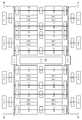
도 1은 대한민국 특허출원 제2003-92375호에 따른 256M 멀티-포트 DRAM의 아키텍쳐를 나타낸 도면이다.1 is a diagram showing the architecture of a 256M multi-port DRAM according to Korean Patent Application No. 2003-92375.
도 1을 참조하면, 제안된 256M 멀티-포트 DRAM은, 각각 다수의 메모리 셀과 로우 디코더(RDEC)를 포함하며, 코어 영역을 4분할하고 있는 각 사분면에 일정 갯수만큼 로우 방향(도면에서는 좌우 방향)으로 배치된 다수의 뱅크(bank0∼bank15)와, 1, 3사분면과 2, 4사분면 사이에 코어 영역을 양분하도록 배치되어 인가된 커맨드, 어드레스 등을 이용하여 내부 커맨드 신호, 내부 어드레스 신호, 제어신호를 생성하여 메모리 소자를 이루는 각 구성 요소들의 동작을 중재하기 위한 중재부(100)와, 각 사분면의 가장자리에 배치되어 각각 다른 타겟 디바이스와 독립적인 통신을 수행하기 위한 다수의 포트(port0∼port7)와, 각 사분면에 대응하는 뱅크와 포트 사이에 로우 방향으로 배치되어 병렬 데이터 전송을 수행하기 위한 제1 내지 제4 글로벌 데이터 버스(GIO_UL, GIO_UR, GIO_DL, GIO_DR)와, 로우 방향으로 인접한 두 글로벌 데이터 버스 사이에 배치되어 두 글로벌 데이터 버스를 선 택적으로 연결하기 위한 제1 및 제2 글로벌 데이터 버스 연결부(PR_U, PR_D)와, 각 뱅크의 컬럼 방향(도면에서는 상하 방향)으로 배치되어 뱅크 내부의 데이터 전송을 수행하기 위한 다수의 트랜스퍼 버스(TB)와, 컬럼 방향으로 인접한 두 뱅크 사이에 배치되어 두 뱅크 각각의 트랜스퍼 버스(TB)를 선택적으로 연결하기 위한 다수의 트랜스퍼 버스 연결부(TG)와, 각 뱅크와 해당 뱅크가 속한 사분면의 글로벌 데이터 버스 사이에 배치되어 각 트랜스퍼 버스(TB)와 해당 글로벌 데이터 버스 사이의 데이터 교환을 수행하기 위한 다수의 버스 연결부(TL)와, 각 포트와 그 포트가 속한 사분면의 글로벌 데이터 버스 사이에 배치되어 해당 포트와 글로벌 데이터 버스 사이의 데이터 송수신을 수행하기 위한 다수의 데이터 전달부(TR)를 구비한다.Referring to FIG. 1, the proposed 256M multi-port DRAM each includes a plurality of memory cells and a row decoder (RDEC), each of which is divided into four quadrants of the core region in a number of row directions (left and right directions in the figure). Internal command signal, internal address signal, and control by using a plurality of banks bank0 to bank15 arranged in a bank) and a command, an address, etc., which are arranged to divide the core area between the first, third and second quadrants.
이하, 상기와 같은 256M 멀티-포트 DRAM의 세부 구성을 살펴본다.Hereinafter, a detailed configuration of the 256M multi-port DRAM as described above will be described.
16개의 뱅크(bank0∼bank15) 각각은 16M(8k 로우×2k 컬럼)의 DRAM 셀과 로우 디코더(RDEC)를 포함하며, 각 뱅크 내부에는 통상의 DRAM 코어 영역에서 필수적인 비트라인 감지증폭기, 이퀄라이져 등의 코어 회로를 구비한다. 뱅크(bank0∼bank15)는 코어 영역을 4분할하고 있는 각 사분면에 4개씩 로우 방향으로 배치된다. 구체적으로, 코어 영역의 1사분면(좌측위)에는 뱅크0, 뱅크2, 뱅크4, 뱅크6가, 2사분면(우측위)에는 뱅크8, 뱅크10, 뱅크12, 뱅크14가, 3사분면(좌측아래)에는 뱅크1, 뱅크3, 뱅크5, 뱅크7이, 4사분면(우측아래)에는 뱅크9, 뱅크11, 뱅크13, 뱅크15가 각각 배치된다. 한편, 로우 디코더(RDEC)는 각 뱅크의 일측에 인접 뱅크의 로우 디코더(RDEC)와 짝을 이루도록 배치하는 것이 바람직하다. 그리고, 하나의 페이지(컬럼)는 4개의 세그먼트(각 세그먼트는 512 개의 셀로 이루어짐)로 구분된다.Each of the 16 banks bank0 to bank15 includes 16M (8k low × 2k columns) of DRAM cells and a row decoder (RDEC), each of which includes a bit line sense amplifier, an equalizer, etc., which is essential in a conventional DRAM core area. It has a core circuit. Banks bank0 to bank15 are arranged in the row direction, four in each quadrant that divides the core region into four. Specifically, in the first quadrant of the core region (upper left),
또한, 중재부(100)는 패킷 형태로 전송된 커맨드, 어드레스 등을 이용하여 내부 활성화 커맨드 신호(ACT), 내부 비활성화 커맨드 신호(PCG), 내부 리드 커맨드 신호(RD), 내부 라이트 커맨드 신호(WD) 등의 내부 커맨드 신호와, 활성화 어레이 어드레스(AAA), 비활성화 어레이 어드레스(PAA), 리드 어레이 어드레스(RAA), 라이트 어레이 어드레스(WAA), 로우 어드레스(RA), 리드 세그먼트 어드레스(RSA), 라이트 세그먼트 어드레스(WSA) 등의 내부 어드레스 신호와, 트랜스퍼 게이트 제어신호(TGC), 파이프 레지스터 플래그 신호(PRFG), 파이프 레지스터 데이터 구동신호(DP), DRAM 코어 테스트 모드 플래그 신호(DTM) 등의 제어신호를 생성하며, 메모리 소자를 이루는 각 구성 요소들의 동작을 중재하는 컨트롤 블럭이다.In addition, the
또한, 포트(port0∼port7)는 각 사분면의 다이(die) 가장자리 부분(해당 사분면의 모든 뱅크가 공유하는 장축변 부분)에 각각 두개씩 배치된다. 구체적으로, 1사분면에는 port0, port2가, 2사분면에는 port4, port6이, 3사분면에는 port1, port3이, 4사분면에는 port5, port7이 각각 배치된다. 각 포트는 직렬 I/O 인터페이스를 지원하며, 각각 다른 타겟 디바이스(예컨대, 칩셋, 그래픽 칩 등)와 독립적인 통신을 수행한다. 한편, 포트(port0∼port7)가 직렬 입/출력 인터페이스를 지원하도록 하는 경우, 각 포트(port0∼port7)는 데이터, 어드레스, 커맨드 등에 대응하는 다수의 패드와, 패드에 전달된 송/수신 신호를 버퍼링하기 위한 패드 버퍼(리드 버퍼, 라이트 버퍼)와, 수신된 데이터를 디코딩하기 위한 디코더와, 송신할 데이터를 인코딩하기 위한 인코더와, 수신된 직렬 데이터를 병렬 데이터로 변환하고 송신할 병렬 데이터를 직렬 데이터로 변환하기 위한 데이터 변환기 등을 구비한다.In addition, two
또한, 1사분면의 뱅크와 포트 사이에는 제1 글로벌 데이터 버스(GIO_UL)가, 2사분면에는 제2 글로벌 데이터 버스(GIO_UR)가, 3사분면에는 제3 글로벌 데이터 버스(GIO_DL)가, 4사분면에는 제4 글로벌 데이터 버스(GIO_DR)가 배치된다. 제1 내지 제4 글로벌 데이터 버스(GIO_UL, GIO_UR, GIO_DL, GIO_DR)는 각각 해당 사분면의 뱅크, 포트 및 글로벌 데이터 버스 연결부(PR_U, PR_D)와 접속되는 양방향 데이터 버스(512 비트)이다.In addition, the first global data bus GIO_UL is interposed between the banks and ports in the first quadrant, the second global data bus GIO_UR is in the second quadrant, the third global data bus GIO_DL is in the third quadrant, and 4 The global data bus GIO_DR is arranged. The first to fourth global data buses GIO_UL, GIO_UR, GIO_DL, and GIO_DR are bidirectional data buses (512 bits) connected to banks, ports, and global data bus connection units PR_U and PR_D of the corresponding quadrants, respectively.
한편, 제1 글로벌 데이터 버스(GIO_UL)와 제2 글로벌 데이터 버스(GIO_UR)는 제1 글로벌 데이터 버스 연결부(PR_U)를 통해 연결될 수 있으며, 제3 글로벌 데이터 버스(GIO_DL)와 제4 글로벌 데이터 버스(GIO_DR)는 제2 글로벌 데이터 버스 연결부(PR_D)를 통해 연결될 수 있다. 제1 및 제2 글로벌 데이터 버스 연결부(PR_U, PR_D)는 글로벌 데이터 버스의 라인수(512 개)에 대응하는 양방향 파이프 레지스터를 구비한다.Meanwhile, the first global data bus GIO_UL and the second global data bus GIO_UR may be connected through the first global data bus connection unit PR_U, and the third global data bus GIO_DL and the fourth global data bus ( The GIO_DR may be connected through the second global data bus connection unit PR_D. The first and second global data bus connections PR_U and PR_D have bidirectional pipe registers corresponding to the number of lines (512) of the global data bus.
또한, 트랜스퍼 버스(TB)는 각 뱅크의 비트라인 감지증폭기와 해당 뱅크에 대응하는 버스 연결부(TL)를 연결하는 로컬 데이터 버스이다. 트랜스퍼 버스(TB)의 라인수는 하나의 세그먼트에 해당하는 셀의 수(예컨대, 512 개)와 동일하며, 차동 버스로 구현된다.In addition, the transfer bus TB is a local data bus that connects the bit line sense amplifiers of each bank and the bus connection unit TL corresponding to the corresponding bank. The number of lines of the transfer bus TB is equal to the number of cells (eg, 512) corresponding to one segment, and is implemented as a differential bus.
또한, 트랜스퍼 버스 연결부(TG)는 트랜스퍼 버스(TB)의 라인수 만큼의 모스 트랜지스터로 구현할 수 있다. 트랜스퍼 버스(TB)가 차동 버스이므로, 하나의 트랜스퍼 버스 연결부(TG)는 총 512쌍의 모스 트랜지스터로 구현할 수 있다. 이러한 이 유로 트랜스퍼 버스 연결부(TG)를 트랜스퍼 게이트로 칭하기로 한다.In addition, the transfer bus connection unit TG may be implemented with as many MOS transistors as the number of lines of the transfer bus TB. Since the transfer bus TB is a differential bus, one transfer bus connection TG may be implemented with a total of 512 MOS transistors. For this reason, the transfer bus connection TG will be referred to as a transfer gate.
또한, 버스 연결부(TL)는 512개의 트랜스퍼 래치가 1세트이고 총 16세트가 구비된다. 각 트랜스퍼 래치는 리드용 버스 연결회로(DRAM의 IO 감지증폭기에 해당함)와 라이트용 버스 연결회로(DRAM의 라이트 드라이버에 해당함)로 구성된다. 여기서, 리드용 버스 연결회로는 트랜스퍼 버스(TB)에 실린 리드 데이터를 감지하여 래치하기 위한 리드 감지증폭기 및 래치된 데이터를 해당 뱅크가 속한 사분면의 글로벌 데이터 버스로 드라이빙하기 위한 리드 드라이버를 구비한다. 또한, 라이트용 버스 연결회로는 글로벌 데이터 버스에 실린 라이트 데이터를 감지하여 래치하기 위한 라이트 래치와, 트랜스퍼 버스(TB)로 라이트 데이터를 드라이빙하기 위한 라이트 드라이버를 구비한다.In addition, the bus connection TL is provided with one set of 512 transfer latches and a total of 16 sets. Each transfer latch consists of a lead bus connection circuit (corresponding to the IO sense amplifier of the DRAM) and a bus bus circuit (corresponding to the write driver of the DRAM). Here, the read bus connection circuit includes a read detection amplifier for sensing and latching read data loaded on the transfer bus TB, and a read driver for driving the latched data to a global data bus of the quadrant to which the corresponding bank belongs. In addition, the write bus connection circuit includes a write latch for sensing and latching write data on the global data bus, and a write driver for driving write data to the transfer bus TB.
또한, 데이터 전달부(TR)는 그에 대응하는 포트에 인가된 라이트 데이터를 글로벌 데이터 버스로 전달하기 위한 512개의 송신기(Tx)와 글로벌 데이터 버스로부터 인가된 리드 데이터를 수신하여 해당 포트로 전달하기 위한 512개의 수신기(Rx)를 구비한다.In addition, the data transfer unit TR is configured to receive 512 transmitters Tx for transferring write data applied to a corresponding port to the global data bus and read data applied from the global data bus to the corresponding port. It has 512 receivers Rx.
이외에도 도시되지는 않았으나, 제안된 256M 멀티-포트 DRAM은 다이의 각 모서리 부분에 배치되며, 외부 전압을 인가 받아 내부 전압을 생성하기 위한 전압 생성기, 1사분면 및 2사분면에 대응하는 포트 사이 그리고 3사분면 및 4사분면에 대응하는 포트 사이에 배치된 테스트 로직, 다이의 가장자리에 배치된 클럭 패드를 비롯한 각종 패드 등을 더 구비한다.Although not shown, the proposed 256M multi-port DRAM is disposed at each corner of the die, and is a voltage generator for generating an internal voltage by applying an external voltage, between ports corresponding to the first and second quadrants, and the third quadrant. And test pads disposed between ports corresponding to the quadrants, various pads including clock pads disposed at edges of the die, and the like.
또한, 각 사분면에는 중재부(100)로부터 뱅크에 이르는 커맨드 라인(ACT, PCG, RD, WD)과, 중재부(100)로부터 뱅크에 이르는 어드레스 라인(AAA<0:1>, PAA<0:1>, RAA<0:1>, WAA<0:1>, RA<0:12>, RSA<0:1>, WSA<0:1>)이 구비된다. 그리고, 중재부(100) 좌우측에는 각각 중재부(100)로부터 트랜스퍼 버스 연결부(TG)에 이르는 트랜스퍼 게이트 제어라인(TGC<0:3>)이 구비된다.In addition, each quadrant has command lines (ACT, PCG, RD, WD) from the
도 2는 상기 도 1에 도시된 256M 멀티-포트 DRAM의 컬럼 구성 단위인 세그먼트와 트랜스퍼 버스(TB)의 관계를 설명하기 위한 도면이다.FIG. 2 is a diagram for explaining a relationship between a segment and a transfer bus TB, which are column units of the 256M multi-port DRAM shown in FIG. 1.
도 2를 참조하면, 제안된 256M 멀티-포트 DRAM은 기존의 일반적인 DRAM과 같이 다수의 메모리 셀 어레이(200)와 비트라인 감지증폭기 어레이(210)를 구비한다. 하나의 메모리 셀 어레이(200)를 기준으로 보면, 한쌍의 트랜스퍼 버스(TB<0>, TBb<0>)는 메모리 셀 어레이(200) 상하부에 배치된 4개의 비트라인 감지증폭기(BLSA)와 연결된다(박스 A 참조). 이 4개의 비트라인 감지증폭기(BLSA)는 각각 다른 세그먼트 선택신호(SGS<0:3>) - 기존의 일반적인 DRAM의 컬럼선택신호(Yi)에 대응하는 신호임 - 에 제어 받는다. 따라서, 2k 컬럼의 경우, 하나의 로우와 하나의 세그먼트가 선택되면 동시에 512개의 셀이 선택되어 그에 대응하는 512 비트의 트랜스퍼 버스(TB<0:511>)와 데이터 교환이 이루어지게 된다.Referring to FIG. 2, the proposed 256M multi-port DRAM has a plurality of
한편, 1사분면의 각 뱅크에 대응하는 트랜스퍼 버스(TB)는 동일 컬럼축 상에 배치된 3사분면의 각 뱅크에 대응하는 트랜스퍼 버스(TB)와 트랜스퍼 게이트(TG)를 통해 연결될 수 있다(512개의 TG가 1세트로 구성되며, 총 8세트임). 즉, 트랜스퍼 게이트(TG)는 동일 컬럼축 상에 배치된 두 뱅크(이를 어레이라 정의함)에 대응하는 트랜스퍼 버스(TB) 사이에 배치되어 두 트랜스퍼 버스(TB)를 선택적으로 연결한다. 트랜스퍼 게이트(TG)를 제어하기 위한 제어신호(TGC)는 중재부(100)에서 생성된다.Meanwhile, the transfer bus TB corresponding to each bank of the first quadrant may be connected through the transfer bus TB and the transfer gate TG corresponding to each bank of the three quadrants disposed on the same column axis (512 units). TG consists of 1 set, total 8 sets). That is, the transfer gate TG is disposed between the transfer buses TB corresponding to two banks (defined as arrays) disposed on the same column axis to selectively connect the two transfer buses TB. The control signal TGC for controlling the transfer gate TG is generated in the
이하, 상기와 같이 구성된 256M 멀티-포트 DRAM의 동작을 살펴본다.Hereinafter, the operation of the 256M multi-port DRAM configured as described above will be described.
도 3a는 상기 도 2에 도시된 256M 멀티-포트 DRAM의 노말 리드 경로를 나타낸 도면이며, 도 3b는 노말 라이트 경로를 나타낸 도면이다.3A illustrates a normal read path of the 256M multi-port DRAM illustrated in FIG. 2, and FIG. 3B illustrates a normal write path.
우선, 포트 port0를 통해 뱅크 bank0에 있는 특정 세그먼트의 데이터(512 비트)를 리드하는 경우를 가정한다.First, it is assumed that the data (512 bits) of a specific segment in the bank bank0 is read through the port port0.
도 3a를 참조하면, 포트 port0을 통해 리드 동작과 관련된 커맨드, 어드레스 등이 패킷 형태로 인가되면, 중재부(100)는 먼저 뱅크 bank0에 대한 내부 활성화 커맨드 신호(ACT), 활성화 어레이 어드레스(AAA) 및 로우 어드레스(RA)를 생성하여 특정 로우(워드라인, WL)를 활성화시키고, 이어서 뱅크 bank0에 대한 내부 리드 커맨드 신호(RD), 리드 어레이 어드레스(RAA) 및 리드 세그먼트 어드레스(RSA)를 생성한다. 이에 따라, 비트라인 감지증폭기(BLSA)는 리드 세그먼트 어드레스(RSA)에 대응하는 세그먼트의 512 비트 데이터를 감지증폭하여 트랜스퍼 버스(TB, TBb)로 구동한다. 한편, 뱅크 bank0의 버스 연결부(TL)는 뱅크 bank0의 트랜스퍼 버스(TB, TBb)에 실린 리드 데이터를 감지하여 제1 글로벌 데이터 버스(GIO_UL)로 데이터를 구동한다. 이어서, 제1 글로벌 데이터 버스(GIO_UL)에 전달된 리드 데이터는 포트 port0에 대응하는 데이터 전달부(TR)의 수신기(Rx)를 거쳐 포트 port0 내의 리드 버퍼에 저장되고, 리드 버퍼에 저장된 데이터는 일정단위의 패킷으로 변환되어 직렬 데이터 형태로 포트 port0와 연결된 타겟 디바이스에 전송된다. 이후, 중재부(100)는 내부 비활성화 커맨드 신호(PCG), 비활성화 어레이 어드레스(PAA)를 생성하여 해당 어레이의 로우를 비활성화시킨다. 이때, 해당 어레이의 트랜스퍼 버스 연결부(TG)는 스위치-오프 상태가 되어 뱅크 bank0의 트랜스퍼 버스(TB, TBb)와 동일 어레이 내의 뱅크 bank1의 트랜스퍼 버스(TB, TBb) 사이의 연결이 끊어지도록 한다. 미설명 도면 부호 'BL, BLb'는 비트라인 쌍, 'T'는 셀 트랜지스터, 'C'는 셀 캐패시터를 각각 나타낸 것이다.Referring to FIG. 3A, when a command, an address, and the like related to a read operation are applied in the form of a packet through the port port0, the
다음으로, 포트 port0를 통해 뱅크 bank0에 있는 특정 세그먼트에 데이터(512 비트)를 라이트하는 경우를 가정한다.Next, assume that the data (512 bits) is written to a specific segment in the bank bank0 through the port port0.
도 3b를 참조하면, 포트 port0을 통해 라이트 동작과 관련된 커맨드, 어드레스, 데이터 등이 패킷 형태로 인가되면, 중재부(100)는 먼저 뱅크 bank0에 대한 내부 활성화 커맨드 신호(ACT), 활성화 어레이 어드레스(AAA) 및 로우 어드레스(RA)를 생성하여 특정 로우(워드라인, WL)를 활성화시키고, 이어서 뱅크 bank0에 대한 내부 라이트 커맨드 신호(WT), 라이트 어레이 어드레스(WAA) 및 라이트 세그먼트 어드레스(WSA)를 생성한다. 이때, 중재부(100)의 스케쥴링에 의해 포트 port0의 라이트 버퍼에 저장된 512 비트 데이터가 라이트 세그먼트 어드레스(WSA)에 대응하는 세그먼트(512 개의 메모리 셀)에 기록된다. 포트 port0에서 병렬 데이터로 변환된 데이터는 데이터 전달부(TR)의 송신기(Tx)를 거쳐 제1 글로벌 데이터 버스(GIO_UL)에 로딩되고, 뱅크 bank0의 버스 연결부(TL)를 통해 다시 뱅크 bank0의 트랜스퍼 버스(TB, TBb)로 구동되며, 뱅크 bank0의 트랜스퍼 버스(TB, TBb)에 로딩된 데이터는 라이트 세그먼트 어드레스(WSA)에 대응하는 비트라인 감지증폭기(BLSA)를 통해 512개의 메모리 셀에 저장된다. 이후, 중재부(100)는 내부 비활성화 커맨드 신호(PCG), 비활성화 어레이 어드레스(PAA)를 생성하여 해당 어레이의 로우를 비활성화시킨다.Referring to FIG. 3B, when a command, an address, data, etc. related to a write operation are applied in the form of a packet through the port port0, the
도 4a는 상기 도 2에 도시된 256M 멀티-포트 DRAM의 크로스 리드 경로를 나타낸 도면이며, 도 4b는 크로스 라이트 경로를 나타낸 도면이다.FIG. 4A illustrates a cross read path of the 256M multi-port DRAM shown in FIG. 2, and FIG. 4B illustrates a cross write path.
우선, 포트 port1을 통해 뱅크 bank0에 있는 특정 세그먼트의 데이터(512 비트)를 리드하는 경우를 가정한다.First, assume a case where data (512 bits) of a specific segment in bank bank0 is read through port port1.
도 4a를 참조하면, 전반적인 동작은 전술한 노멀 리드시와 거의 유사하나, 해당 어레이의 트랜스퍼 버스 연결부(TG)가 스위치-온 상태가 되어 뱅크 bank0의 트랜스퍼 버스(TB, TBb)와 동일 어레이 내의 뱅크 bank1의 트랜스퍼 버스(TB, TBb)가 서로 연결되도록 하는 것이 다르다. 한편, 뱅크 bank1의 트랜스퍼 버스(TB, TBb)에 로딩된 데이터는 뱅크 bank1에 대응하는 버스 연결부(TL), 제3 글로벌 데이터 버스(GIO_DL), 포트 port1에 대응하는 데이터 전달부(TR), 포트 port1을 거쳐 타겟 디바이스로 전달된다.Referring to FIG. 4A, the overall operation is almost similar to that of the normal read described above, but the transfer bus connection TG of the array is switched on so that the banks in the same array as the transfer buses TB and TBb of bank bank0 are shown. It is different that the transfer buses (TB, TBb) of bank1 are connected to each other. Meanwhile, the data loaded on the transfer buses TB and TBb of the bank bank1 includes a bus connection unit TL corresponding to the bank bank1, a third global data bus GIO_DL, a data transfer unit TR corresponding to the port port1, and a port. It is delivered to the target device via port1.
다음으로, 포트 port1을 통해 뱅크 bank0에 있는 특정 세그먼트에 데이터(512 비트)를 라이트하는 경우를 가정한다.Next, assume that the data (512 bits) is written to a specific segment in the bank bank0 through the port port1.
도 4b를 참조하면, 전반적인 동작은 전술한 노멀 라이트시와 거의 유사하나, 역시 해당 어레이의 트랜스퍼 버스 연결부(TG)가 스위치-온 상태가 되어 뱅크 bank0의 트랜스퍼 버스(TB, TBb)와 동일 어레이 내의 뱅크 bank1의 트랜스퍼 버스(TB, TBb)가 서로 연결되도록 하는 것이 다르다. 이 경우, 포트 port1에 인가된 데이터는 포트 port1에 대응하는 데이터 전달부(TR), 제3 글로벌 데이터 버스(GIO_DL), 뱅크 bank1에 대응하는 버스 연결부(TL)를 거쳐 뱅크 bank0의 트랜스퍼 버스(TB, TBb)로 로딩되며, 이후의 과정은 전술한 노멀 라이트시와 동일하다.Referring to FIG. 4B, the overall operation is almost similar to that of normal write described above, but also the transfer bus connection TG of the array is switched on so that it is in the same array as the transfer buses TB and TBb of bank bank0. The difference is that the transfer buses TB and TBb of bank bank1 are connected to each other. In this case, the data applied to the port port1 is transferred through the data transfer unit TR corresponding to the port port1, the third global data bus GIO_DL, and the bus connection unit TL corresponding to the bank bank1, and the transfer bus TB of the bank bank0. , TBb), and the subsequent process is the same as that of the normal write described above.
한편, 제1 글로벌 데이터 버스(GIO_UL)와 제2 글로벌 데이터 버스(GIO_UR) 사이에 데이터 교환이 필요한 경우에는 제1 글로벌 데이터 버스 연결부(PR_U)를 통해 두 글로벌 데이터 버스를 연결하고, 제3 글로벌 데이터 버스(GIO_DL)와 제4 글로벌 데이터 버스(GIO_DR) 사이에 데이터 교환이 필요한 경우에는 제2 글로벌 데이터 버스 연결부(PR_D)를 통해 두 글로벌 데이터 버스를 연결하면 된다.Meanwhile, when data exchange is required between the first global data bus GIO_UL and the second global data bus GIO_UR, the two global data buses are connected through the first global data bus connection unit PR_U, and the third global data is connected. When data exchange is required between the bus GIO_DL and the fourth global data bus GIO_DR, two global data buses may be connected through the second global data bus connection unit PR_D.
전술한 바와 같이 제안된 멀티-포트 DRAM은 모든 포트(port0∼port7)에서 모든 세그먼트를 액세스할 수 있으며, 다수의 포트를 통해 독립적인 액세스가 가능하기 때문에 - 글로벌 데이터 버스가 중복 사용되지 않는 범위에서 - 동시에 멀티 액세스가 가능하다. 또한, 새로운 아키텍쳐의 적용을 통해 코어 영역의 각 사분면에서 512 비트의 데이터를 병렬로 처리할 수 있으며, 포트에서는 직렬로 데이터를 입/출력할 수 있다. 따라서, 레이아웃 면적 증가를 최소화하고, 패키징이 용이하며, 데이터 버스에서의 데이터 선로간 스큐 문제를 유발하지 않으면서 밴드폭을 크게 증가시킬 수 있다.As mentioned above, the proposed multi-port DRAM can access all segments from all ports (port0 to port7), and can be accessed independently through multiple ports-in the range that the global data bus is not used redundantly. -Multi access is possible at the same time. In addition, the new architecture enables the processing of 512 bits of data in parallel in each quadrant of the core area, and the input and output of data in the serial port. Therefore, it is possible to minimize the layout area increase, to easily package, and to increase the bandwidth without causing the skew problem between data lines on the data bus.
한편, 전술한 바와 같이 제안된 멀티-포트 DRAM은 512 비트에 이르는 광폭의 글로벌 데이터 버스를 구비하고 있다. 기존에 제안된 가장 밴드폭이 큰 DRAM(DDR2)의 글로벌 데이터 버스가 64개의 버스 라인을 갖고 있는 것에 비하면 버스 라인의 수가 매우 많음을 알 수 있다.On the other hand, as described above, the proposed multi-port DRAM has a wide global data bus of up to 512 bits. It can be seen that the number of bus lines is much larger than that of the previously proposed global data bus of the largest bandwidth DRAM (DDR2) having 64 bus lines.
글로벌 데이터 버스의 라인수가 64개 이하인 경우에는 버스를 통해 전달되는 데이터가 코어 전압(Vcc) 레벨로 풀 스윙하더라도 그 전류 소모량이 그다지 큰 문제가 되질 않았으나, 글로벌 데이터 버스의 라인수가 64개 보다 늘어나게 되면, 즉 128, 256, 512개 등으로 늘어나면 데이터 전송에 많은 전류가 소모되어 전력 문제를 야기하게 된다.If the number of lines in the global data bus is 64 or less, even if the data transferred through the bus is full swing to the core voltage (Vcc) level, the current consumption is not a big problem. In other words, if the number is increased to 128, 256, 512, etc., a large amount of current is consumed in data transmission, causing power problems.
이러한 광폭의 글로벌 데이터 버스에서의 전력 문제를 해결하기 위하여 본 발명의 출원인은 기존의 전압 드라이빙 방식이 아닌 전류 센싱 방식을 사용하는 글로벌 데이터 버스 송/수신 구조를 제안한 바 있다(2003년 12월 22일자 출원된 대한민국 특허출원 제2003-94697호 참조).In order to solve the power problem in the wide global data bus, the applicant of the present invention has proposed a global data bus transmit / receive structure using a current sensing method instead of a conventional voltage driving method (December 22, 2003) See Korean Patent Application No. 2003-94697 filed).
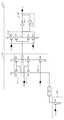
도 5는 대한민국 특허출원 제2003-94697호에 따른 송신기 및 수신기의 회로 구성을 나타낸 도면이다.5 is a diagram illustrating a circuit configuration of a transmitter and a receiver according to Korean Patent Application No. 2003-94697.
도 5를 참조하면, 제안된 송신기(500)는 접지전압단(vss)과 글로벌 데이터 버스(GIO) 사이에 연결되며, 데이터 신호(cdio)를 게이트 입력으로 하는 풀다운 NMOS 트랜지스터(MN1)를 구비한다.Referring to FIG. 5, the proposed
한편, 제안된 수신기는 글로벌 데이터 버스(GIO)에 흐르는 전류를 센싱하여 글로벌 데이터 버스(GIO)에 실린 데이터를 검출하기 위한 수신부(510)와, 수신부(510)에 수신된 데이터를 래치하기 위한 래치부(520)를 구비한다.On the other hand, the proposed receiver senses the current flowing in the global data bus (GIO), the
여기서, 수신부(510)는 글로벌 데이터 버스(GIO)에 흐르는 전류를 출력 노드(A)에 미러링하기 위한 전류미러부(512)와, 글로벌 데이터 버스(GIO)에 흐르는 전류량을 결정하기 위한 부하부(514)와, 데이터 캡쳐 신호(cp)에 응답하여 출력 노드(A)의 전류 패스를 제공하기 위한 스위칭부(516)를 구비한다.Here, the
또한, 래치부(520)는 데이터 캡쳐 신호(cp, cpb)에 응답하여 수신부(510)의 출력 노드(A)에 실린 신호를 반전시키기 위한 반전부(522)와, 반전부(522)의 출력신호를 반전 래치하기 위한 반전 래치부(524)를 구비한다.In addition, the
한편, 수신부(510)의 전류 미러부(512)는 소오스가 전원전압단(vtl)에 접속되며 드레인과 게이트가 다이오드 접속된 PMOS 트랜지스터(MP1)와, 소오스가 전원전압단(vtl)에 접속되며 드레인이 출력 노드(A)에 접속된 PMOS 트랜지스터(MP2)를 구비한다.On the other hand, the
그리고, 수신부(510)의 부하부(214)는 소오스가 PMOS 트랜지스터(MP1)의 드레인에 접속되고, 드레인이 글로벌 데이터 버스(GIO) 사이에 접속되며, 게이트로 기준전압(vrtb)을 인가 받는 NMOS 트랜지스터(MN2)와, 소오스가 PMOS 트랜지스터(MP2)의 드레인(출력 노드 A)에 접속되며, 게이트로 기준전압(vrtb)을 인가 받는 NMOS 트랜지스터(MN3)를 구비한다. 즉, 부하부(214)는 액티브 저항으로 구현할 수 있으며, 기준전압(vrtb)은 항상 일정한 레벨을 유지하는 정전압이며, 그 레벨은 버스의 길이, 동작주파수 등을 고려하여 최소한의 전류가 소모되도록 하는 범위에서 결정한다.In the load unit 214 of the
그리고, 수신부(510)의 스위칭부(516)는 소오스가 NMOS 트랜지스터(MN3)의 드레인에 접속되고, 드레인이 접지전압단(vss)에 접속되며, 게이트로 데이터 캡쳐 신호(cp)를 인가 받는 NMOS 트랜지스터(MN4)를 구비한다.The
한편, 래치부(520)의 반전부(522)는 소오스가 내부전압단(vtl)에 접속되고, 데이터 캡쳐 신호의 반전신호(cpb)를 게이트 입력으로 하는 PMOS 트랜지스터(MP3) 와, 소오스가 PMOS 트랜지스터(MP3)의 드레인에 접속되고, 드레인이 출력 노드(B)에 접속되며, 수신부(510)의 출력신호를 게이트 입력으로 하는 PMOS 트랜지스터(MP4)와, 소오스가 접지전압단(vss)에 접속되고, 데이터 캡쳐 신호(cp)를 게이트 입력으로 하는 NMOS 트랜지스터(MN5)와, 소오스가 NMOS 트랜지스터(MN5)의 드레인에 접속되고, 드레인이 출력 노드(B)에 접속되며, 수신부(510)의 출력신호를 게이트 입력으로 하는 NMOS 트랜지스터(MN4)를 구비한다.On the other hand, the
그리고, 래치부(520)의 반전 래치부(524)는 2개의 인버터(INV1, INV2)로 구현할 수 있다.In addition, the inverting
도 6는 상기 도 5의 회로의 시뮬레이션 결과를 타나낸 도면이다.6 is a diagram illustrating a simulation result of the circuit of FIG. 5.
데이터 캡쳐 신호(cp)는 라이트 커맨드 또는 리드 커맨드가 인가되었을 때, 일정 시간(예컨대, 1tCK) 동안 활성화되는 하이 액티브 펄스이다.The data capture signal cp is a high active pulse that is activated for a predetermined time (
이하, 도 6을 참조하여 상기 도 5의 회로의 동작을 살펴본다.Hereinafter, the operation of the circuit of FIG. 5 will be described with reference to FIG. 6.
우선, 데이터 신호(cdio)가 논리레벨 하이가 되면 송신기(500)의 NMOS 트랜지스터(MN1)가 턴온되어 글로벌 데이터 버스(GIO)에 전류가 흐르게 된다. 즉, 전원전압단(vtl), PMOS 트랜지스터(MP1), NMOS 트랜지스터(MN2), 글로벌 데이터 버스(GIO), NMOS 트랜지스터(MN1), 접지전압단(vss)에 이르는 전류 패스가 형성된다. 이에 따라서, 글로벌 데이터 버스(GIO) 및 수신부(510)의 전류 미러부(512)의 PMOS 트랜지스터(MP1)의 드레인단의 전위가 vtl-Vtp(PMOS 트랜지스터의 문턱전압) 이하로 떨어지고, 전류 미러부(212)의 두 PMOS 트랜지스터(MP1, MP2)가 턴온되어 수신부(210)의 출력 노드(A)의 전위가 상승하게 된다.First, when the data signal cdio becomes logic level high, the NMOS transistor MN1 of the
이때, 데이터 캡쳐 신호(cp)가 논리레벨 하이로 활성화되어 NMOS 트랜지스터(MN4)가 턴온되면, PMOS 트랜지스터(MP2)와 NMOS 트랜지스터(MN4)의 출력 노드(A)에 대한 충/방전 경합이 이루어지나 PMOS 트랜지스터(MP2)의 사이즈를 크게 설계하면 출력 노드(A)의 전위가 논리레벨 로우로 급격히 방전되는 것을 방지할 수 있다.At this time, when the data capture signal cp is activated at a logic level high and the NMOS transistor MN4 is turned on, charge / discharge contention is performed between the PMOS transistor MP2 and the output node A of the NMOS transistor MN4. By designing the size of the PMOS transistor MP2 large, it is possible to prevent the potential of the output node A from being rapidly discharged to the logic level low.
한편, 데이터 캡쳐 신호(cp)가 논리레벨 하이로 활성화되면 래치부(520)의 반전부(522)의 NMOS 트랜지스터(MN5, MN6)가 턴온되며, 이때 수신부(510)의 출력신호는 논리레벨 하이 상태이므로, 반전부(522)의 출력 노드(B)는 논리레벨 로우가 된다. 또한, 반전 래치부(524)에서는 논리레벨 하이값을 출력하며, 데이터 캡쳐 신호(cp)가 다시 활성화될 때까지 그 값을 유지한다.Meanwhile, when the data capture signal cp is activated at a logic level high, the NMOS transistors MN5 and MN6 of the
다음으로, 데이터 신호(cdio)가 논리레벨 로우가 되면 송신기(500)의 NMOS 트랜지스터(MN1)가 턴오프되어 글로벌 데이터 버스(GIO) 및 수신부(510)의 전류 미러부(512)의 PMOS 트랜지스터(MP1)의 드레인단의 전위가 상승하게 되고, 전류 미러부(512)의 두 PMOS 트랜지스터(MP1, MP2)가 턴오프된다.Next, when the data signal cdio becomes a logic level low, the NMOS transistor MN1 of the
이때, 데이터 캡쳐 신호(cp)가 논리레벨 하이로 활성화되어 NMOS 트랜지스터(MN4)가 턴온되며, 이에 따라 수신부(510)의 출력 노드(A)의 전위가 떨어지게 된다. 또한, 데이터 캡쳐 신호(cp) 논리레벨 하이로 활성화되면 래치부(520)의 반전부(522)의 PMOS 트랜지스터(MP3, MP4)가 턴온되어 수신부(510)의 출력신호를 반전시켜 반전부(522)의 출력 노드(B)를 논리레벨 하이로 만든다. 또한, 반전 래치부(524)에서는 논리레벨 로우값을 출력하며, 데이터 캡쳐 신호(cp) 가 다시 활성화될 때까지 그 값을 유지한다.At this time, the data capture signal cp is activated to a logic level high, so that the NMOS transistor MN4 is turned on, and thus the potential of the output node A of the
전술한 수신기 회로에서 사용한 내부전압(vtl)은 코어전압(vcc, 2.5V)에 비해 다소 낮은 1.8V 정도의 레벨을 가진다. 따라서, 데이터 신호(cdio)가 논리레벨 하이인 경우, 글로벌 데이터 버스(GIO)의 전위는 0V보다 약간 높은 레벨이며, 데이터 신호(cdio)가 논리레벨 로우인 경우에는 MOS 트랜지스터의 문턱전압을 고려할 때 1V 미만의 레벨을 가질 것이다. 따라서, 본 발명을 적용하면 종래기술과 같이 글로벌 데이터 버스(GIO)가 코어 전압(vcc) 레벨로 풀 스윙하지 않고, 스윙 폭이 매우 작기 때문에 글로벌 데이터 버스(GIO)의 충방전에 소모되는 전류를 최소화할 수 있다. 이처럼 전류 소모를 크게 줄임으로써 글로벌 데이터 버스(GIO)의 라인수를 128, 256, 512개 등으로 확장할 때 수반되는 전력 소모 문제를 해결할 수 있다.The internal voltage vtl used in the above-described receiver circuit has a level of about 1.8V which is somewhat lower than the core voltage vcc, 2.5V. Therefore, when the data signal cdio is at logic level high, the potential of the global data bus GIO is at a level slightly higher than 0 V. When the data signal cdio is at logic level low, the threshold voltage of the MOS transistor is considered. Will have a level of less than 1V. Therefore, according to the present invention, since the global data bus GIO does not full swing to the core voltage vcc level and the swing width is very small, the current consumed during charging and discharging of the global data bus GIO is reduced. It can be minimized. This significant reduction in current consumption solves the power consumption issues associated with expanding the number of lines in the global data bus (GIO) to 128, 256, or 512.
한편, 송신기(500)에 풀다운 드라이버가 아닌 풀업 드라이버만을 사용하고, 수신부(510)의 회로를 변경하는 경우에도 전류 소모를 줄일 수 있으나, 풀업 드라이버를 사용하는 경우, 글로벌 데이터 버스(GIO)를 구동하기 위하여 풀다운 드라이버에 비해 2개 이상 큰 사이즈의 드라이버 트랜지스터를 필요로 하기 때문에 반도체 메모리 칩의 면적을 고려할 때 적합하지 않다.On the other hand, only a pull-up driver, not a pull-down driver, is used for the
한편, 상기 도 1에 도시된 256M 멀티-포트 DRAM은 글로벌 데이터 버스(GIO)와 송수신을 수행하는 구조를 2개 포함하고 있다. 즉, 각 뱅크와 해당 뱅크가 속한 사분면의 글로벌 데이터 버스 사이에 배치되어 각 트랜스퍼 버스(TB)와 해당 글로벌 데이터 버스 사이의 데이터 교환을 수행하기 위한 다수의 버스 연결부(TL)가 그 하나이며, 각 포트와 그 포트가 속한 사분면의 글로벌 데이터 버스 사이에 배치되 어 해당 포트와 글로벌 데이터 버스 사이의 데이터 송수신을 수행하기 위한 다수의 데이터 전달부(TR)가 나머지 하나이다.Meanwhile, the 256M multi-port DRAM shown in FIG. 1 includes two structures for transmitting and receiving to and from a global data bus (GIO). That is, a plurality of bus connections TL disposed between each bank and the global data bus of the quadrant to which the bank belongs to perform data exchange between each transfer bus TB and the corresponding global data bus are each one. The other one is a plurality of data transfer units disposed between the port and the global data bus of the quadrant to which the port belongs to perform data transmission and reception between the port and the global data bus.
상기 도 5에 도시된 수신기 구조(510, 520)는 버스 연결부(트랜스퍼 래치, TL)와 데이터 전달부(TR)의 수신측에 모두 적용될 수 있으나, 도시된 송신기(500)를 그대로 버스 연결부(트랜스퍼 래치, TL)에 적용할 수는 없다.Although the
따라서, 버스 연결부(트랜스퍼 래치, TL)의 구성 중 로컬 데이터 버스인 트랜스퍼 버스(TB)로부터 글로벌 데이터 버스(GIO)로 데이터를 전달하기 구성, 즉 상기와 같은 전류 센싱 방식의 송수신 구조에 적합한 새로운 리드용 버스 연결회로(일반적인 DRAM의 IO 감지증폭기에 해당함)를 개발할 필요성이 대두되었다.Therefore, a new lead suitable for the transmission / reception structure of the current sensing scheme as described above is configured to transfer data from the transfer bus TB, which is a local data bus, to the global data bus GIO in the configuration of the bus connection unit (transfer latch, TL). There is a need to develop a bus connection circuit (corresponding to an IO sense amplifier of a typical DRAM).
본 발명은 상기와 같은 종래기술의 문제점을 해결하기 위하여 제안된 것으로, 전류 센싱 방식의 버스 송수신 구조에 적합한 멀티-포트 메모리 소자의 리드용 버스 연결회로를 제공하는데 그 목적이 있다.
The present invention has been proposed to solve the above problems of the prior art, and an object thereof is to provide a bus connection circuit for a lead of a multi-port memory device suitable for a current sensing bus transmission / reception structure.
상기의 기술적 과제를 달성하기 위한 본 발명의 일 측면에 따르면, 리드 데이터 스트로브신호에 응답하여 로컬 데이터 버스에 실린 리드 데이터를 감지하여 래치하기 위한 리드 데이터 감지/래치수단과, 리드 데이터 드라이빙펄스에 응답하여 상기 리드 데이터 감지/래치수단에 래치된 데이터를 글로벌 데이터 버스로 드라 이빙하되, 상기 래치된 데이터의 논리레벨에 따라 글로벌 데이터 버스에 흐르는 전류의 경로를 연결 또는 차단하기 위한 리드 데이터 구동수단을 구비하는 멀티-포트 메모리 소자의 리드용 버스 연결회로가 제공된다.According to an aspect of the present invention for achieving the above technical problem, the read data detection / latch means for detecting and latching the read data carried on the local data bus in response to the read data strobe signal, and in response to the read data driving pulse Drive data latched to the read data detection / latch means onto a global data bus, the read data driving means for connecting or disconnecting a current path flowing through the global data bus according to the logic level of the latched data. A bus connection circuit for a lead of a multi-port memory device is provided.
바람직하게, 상기 리드 데이터 감지/래치수단은, 상기 리드 데이터 스트로브신호에 응답하여 로컬 데이터 버스에 실린 리드 데이터를 감지 및 래치하기 위한 차동 입력 플립플롭; 상기 차동 입력 플립플롭의 차동 출력신호를 입력으로 하는 전달 인버터; 및 상기 전달 인버터의 출력신호를 래치하기 위한 반전 래치를 구비한다.Advantageously, said read data sensing / latch means comprises: a differential input flip-flop for sensing and latching read data carried on a local data bus in response to said read data strobe signal; A transfer inverter configured to receive a differential output signal of the differential input flip-flop as an input; And an inverting latch for latching an output signal of the transfer inverter.
바람직하게, 상기 리드 데이터 구동수단은, 접지전압단에 접속되며 상기 리드 데이터 드라이빙펄스를 게이트 입력으로 하는 제1 NMOS 트랜지스터와, 상기 NMOS 트랜지스터와 글로벌 데이터 버스 사이에 접속되며 상기 리드 데이터 감지/래치수단의 출력신호를 게이트 입력으로 하는 제2 NMOS 트랜지스터를 구비한다.Preferably, the read data driving means is connected to a ground voltage terminal, the first NMOS transistor having the read data driving pulse as a gate input, and connected between the NMOS transistor and a global data bus, and the read data sensing / latch means. And a second NMOS transistor whose output signal is a gate input.
이하, 본 발명이 속한 기술분야에서 통상의 지식을 가진 자가 본 발명을 보다 용이하게 실시할 수 있도록 하기 위하여 본 발명의 바람직한 실시예를 소개하기로 한다.Hereinafter, preferred embodiments of the present invention will be introduced in order to enable those skilled in the art to more easily carry out the present invention.
도 7은 본 발명의 일 실시예에 따른 멀티-포트 DRAM의 리드용 버스 연결회로를 나타낸 도면이다.FIG. 7 illustrates a bus connection circuit for reading a multi-port DRAM according to an exemplary embodiment of the present invention.
도 7을 참조하면, 본 실시예에 따른 멀티-포트 DRAM의 리드용 버스 연결회로는, 리드 데이터 스트로브신호(iosastp)에 응답하여 트랜스퍼 버스(TB, TBb)에 실 린 리드 데이터를 감지하여 래치하기 위한 리드 데이터 감지/래치부(700)와, 리드 데이터 드라이빙펄스(rdp)에 응답하여 리드 데이터 감지/래치부(700)에 래치된 데이터를 글로벌 데이터 버스로 드라이빙하되, 래치된 데이터의 논리레벨에 따라 글로벌 데이터 버스에 흐르는 전류의 경로를 연결 또는 차단하기 위한 리드 데이터 구동부(750)를 구비한다.Referring to FIG. 7, the read bus connection circuit of the multi-port DRAM according to the present embodiment senses and latches read data loaded on the transfer buses TB and TBb in response to a read data strobe signal iosastp. Drive the data latched to the read data detection /
여기서, 리드 데이터 감지/래치부(700)는 리드 데이터 스트로브신호(iosastp)에 응답하여 트랜스퍼 버스(TB, TBb)에 실린 리드 데이터를 감지 및 래치하기 위한 차동 입력 플립플롭(710)과, 차동 입력 플립플롭(710)의 차동 출력신호를 입력으로 하는 전달 인버터(720)와, 전달 인버터(720)의 출력신호를 래치하기 위한 반전 래치(730)를 구비한다.Here, the read data detection /
또한, 차동 입력 플립플롭(710)은 접지전압단(VSSTL)에 접속되며 리드 데이터 스트로브신호(iosastp)를 게이트 입력으로 하는 싱크 NMOS 트랜지스터(MN15)와, 싱크 NMOS 트랜지스터(MN15)의 일측에 접속되며 각각 트랜스퍼 버스에 실린 신호(TB, TBb)를 게이트 입력으로 하는 차동 입력 NMOS 트랜지스터(MN11, MN12)와, 정/부 출력단(X/Y)에 크로스 커플되어 인버터 래치를 이루는 NMOS 트랜지스터(MN13, MN14) 및 PMOS 트랜지스터(MP11, MP12), 리드 데이터 스트로브신호(iosastp)의 비활성화 구간에서 정/부 출력단(X/Y)을 프리차지하기 위한 PMOS 트랜지스터(MN14, MN13)와, 정 출력단(X)으로 출력되는 신호를 반전시키기 위한 인버터(INV11)를 구비한다.In addition, the differential input flip-
또한, 전달 인버터(720)는 내부전압단(vtl)과 그 출력단 사이에 접속되며 부 출력단(Y)으로 출력되는 신호를 게이트 입력으로 하는 PMOS 트랜지스터(MP15)와, 접지전압단(VSSTL)과 그 출력단 사이에 접속되며 인버터(INV11)의 출력신호를 게이트 입력으로 하는 NMOS 트랜지스터를 구비한다.In addition, the
그리고, 반전 래치(730)는 전달 인버터(720)의 출력단에 접속된 2개의 인버터(INV12, INV13)를 구비한다.The inverting
한편, 리드 데이터 구동부(750)는 접지전압단(VSSTL)에 접속되며 리드 데이터 드라이빙펄스(rdp)를 게이트 입력으로 하는 NMOS 트랜지스터(MN18)와, NMOS 트랜지스터(MN18)와 글로벌 데이터 버스(DQ) 사이에 접속되며 반전 래치(730)의 출력신호를 게이트 입력으로 하는 NMOS 트랜지스터(MN17)를 구비한다.Meanwhile, the read
도 8은 상기 도 7에 도시된 회로의 타이밍 다이어그램으로서, 이하 이를 참조하여 본 실시예에 따른 멀티-포트 DRAM의 리드용 버스 연결회로의 동작을 살펴본다.FIG. 8 is a timing diagram of the circuit shown in FIG. 7. Hereinafter, the operation of the read bus connection circuit of the multi-port DRAM according to the present exemplary embodiment will be described with reference to the timing diagram.
먼저, 리드 데이터 스트로브신호(iosastp)가 논리레벨 로우로 비활성화 된 상태에서는 정 출력단(X)과 부 출력단(Y)은 PMOS 트랜지스터(MN14, MN13)에 의해 논리레벨 하이로 프리차지 되기 때문에 반전 래치(730)에 래치된 값이 그대로 유지된다.First, when the read data strobe signal ioastast is inactivated to a logic level low, the positive output terminal X and the negative output terminal Y are precharged to a logic level high by the PMOS transistors MN14 and MN13. The latched value at 730 is retained.
한편, 리드 데이터 스트로브신호(iosastp)가 논리레벨 하이로 활성화되면, 트랜스퍼 버스에 실린 신호(TB, TBb)의 레벨에 따라 정 출력단(X)과 부 출력단(Y)은 서로 반대의 논리값을 가지게 된다. 정출력 및 부출력은 전달 인버터(720)에서 반전된 후 반전 래치(730)에 저장되며, 이 값은 트랜스퍼 버스에 실린 신호(TB, TBb)가 천이하기 전까지는 그대로 유지된다.On the other hand, when the read data strobe signal (iosastp) is activated at a logic level high, the positive output terminal (X) and the negative output terminal (Y) have opposite logic values according to the levels of the signals TB and TBb loaded on the transfer bus. do. The positive and negative outputs are inverted in the
만일, 반전 래치(730)에 저장된 값이 논리레벨 하이이면 NMOS 트랜지스터(MN17)가 턴온되며, 리드 커맨드 인가시점으로부터 일정시간 후에 리드 데이터 드라이빙펄스(rdp)가 논리레벨 하이로 활성화되면 NMOS 트랜지스터(MN18)까지 턴온되어 글로벌 데이터 버스(DQ)에 전류가 흐르게 된다.If the value stored in the
한편, 반전 래치(730)에 저장된 값이 논리레벨 로우이면 NMOS 트랜지스터(MN17)가 턴오프 되기 때문에 리드 데이터 드라이빙펄스(rdp)가 논리레벨 하이로 활성화되더라도 글로벌 데이터 버스(DQ)에는 더 이상 전류가 흐르지 않게 된다. 이러한 동작의 원리는 상기 도 5 및 도 6에서 충분히 설명한 바 있다.On the other hand, if the value stored in the inverting
결국, 본 실시예에 따른 멀티-포트 DRAM의 리드용 버스 연결회로는 리드 데이터 스트로브신호(iosastp)의 라이징 에지에서 트랜스퍼 버스(TB, TBb)에 실린 데이터를 스트로빙하여 래치하고, 래치된 데이터는 리드 데이터 드라이빙펄스(rdp)가 활성화된 시점에 글로벌 데이터 버스(DQ)로 전송된다.As a result, the read bus connection circuit of the multi-port DRAM according to the present embodiment strobes and latches data loaded on the transfer buses TB and TBb at the rising edge of the read data strobe signal iosastp. The read data driving pulse rdp is transmitted to the global data bus DQ at the time when the read data driving pulse rdp is activated.
본 발명의 기술 사상은 상기 바람직한 실시예에 따라 구체적으로 기술되었으나, 상기한 실시예는 그 설명을 위한 것이며 그 제한을 위한 것이 아님을 주의하여야 한다. 또한, 본 발명의 기술 분야의 통상의 전문가라면 본 발명의 기술 사상의 범위 내에서 다양한 실시예가 가능함을 이해할 수 있을 것이다.Although the technical idea of the present invention has been described in detail according to the above preferred embodiment, it should be noted that the above-described embodiment is for the purpose of description and not of limitation. In addition, those skilled in the art will understand that various embodiments are possible within the scope of the technical idea of the present invention.
예컨대, 전술한 실시예에서는 DRAM 셀을 사용하는 경우를 일례로 들어 설명하였으나, 본 발명은 SRAM을 비롯한 다른 RAM 셀을 사용하는 경우에도 적용된다.For example, in the above-described embodiment, the case of using a DRAM cell has been described as an example, but the present invention is also applied to the case of using other RAM cells including SRAM.
또한, 전술한 실시예에서는 512 비트의 단위 세그먼트를 사용하는 경우를 일례로 들어 설명하였으나, 본 발명은 단위 세그먼트의 비트수를 변경하는 경우에도 적용된다.In the above-described embodiment, the case of using a unit segment of 512 bits is described as an example, but the present invention is also applied to the case of changing the number of bits of the unit segment.
또한, 전술한 실시예에서 사용된 포트의 수, 뱅크의 수 등도 메모리 소자의 용량에 따라 변경될 수 있다.In addition, the number of ports, the number of banks, and the like used in the above-described embodiments may also change according to the capacity of the memory device.
또한, 전술한 실시예에서는 싱크 NMOS 트랜지스터를 사용하는 NMOS 타입의 차동 입력 플립플롭을 사용하는 경우를 일례로 들어 설명하였으나, 소스 PMOS 트랜지스터를 사용하는 PMOS 타입의 차동 입력 플립플롭을 사용하는 경우에도 본 발명은 적용된다.In addition, in the above-described embodiment, the case where a differential input flip-flop of an NMOS type using a sink NMOS transistor is used has been described as an example. However, the present invention also applies to a case of using a differential input flip-flop of a PMOS type that uses a source PMOS transistor. The invention applies.
전술한 본 발명은 전류 센싱 방식의 버스 송수신 구조에 적합한 멀티-포트 메모리 소자의 리드용 버스 연결회로를 제공하며, 이에 따라 광폭의 글로벌 데이터 버스를 사용하는 멀티-포트 메모리 소자의 전류 소모를 크게 줄일 수 있다.
The present invention described above provides a bus connection circuit for a lead of a multi-port memory device suitable for a current sensing bus transmission / reception structure, thereby greatly reducing current consumption of a multi-port memory device using a wide global data bus. Can be.
Claims (8)
Translated fromKoreanPriority Applications (3)
| Application Number | Priority Date | Filing Date | Title |
|---|---|---|---|
| KR1020040031988AKR100605592B1 (en) | 2004-05-06 | 2004-05-06 | Bus Connection Circuit for Leading Multi-Port Memory Devices |
| US10/876,504US7046575B2 (en) | 2004-05-06 | 2004-06-24 | Bus connection circuit for read operation of multi-port memory device |
| TW093118432ATWI287234B (en) | 2004-05-06 | 2004-06-25 | Bus connection circuit for read operation of multi-port memory device and multi-port memory device |
Applications Claiming Priority (1)
| Application Number | Priority Date | Filing Date | Title |
|---|---|---|---|
| KR1020040031988AKR100605592B1 (en) | 2004-05-06 | 2004-05-06 | Bus Connection Circuit for Leading Multi-Port Memory Devices |
Publications (2)
| Publication Number | Publication Date |
|---|---|
| KR20050106918A KR20050106918A (en) | 2005-11-11 |
| KR100605592B1true KR100605592B1 (en) | 2006-07-31 |
Family
ID=35239290
Family Applications (1)
| Application Number | Title | Priority Date | Filing Date |
|---|---|---|---|
| KR1020040031988AExpired - Fee RelatedKR100605592B1 (en) | 2004-05-06 | 2004-05-06 | Bus Connection Circuit for Leading Multi-Port Memory Devices |
Country Status (3)
| Country | Link |
|---|---|
| US (1) | US7046575B2 (en) |
| KR (1) | KR100605592B1 (en) |
| TW (1) | TWI287234B (en) |
Families Citing this family (8)
| Publication number | Priority date | Publication date | Assignee | Title |
|---|---|---|---|---|
| KR100641708B1 (en)* | 2005-04-08 | 2006-11-03 | 주식회사 하이닉스반도체 | Multi-Port Memory Devices |
| EP1727147B1 (en)* | 2005-05-23 | 2011-07-13 | STMicroelectronics (Crolles 2) SAS | Sense amplifier for dynamic memory |
| KR100845796B1 (en)* | 2006-02-07 | 2008-07-14 | 주식회사 하이닉스반도체 | Circuit and Method for Inputting/Outputting Data of Semiconductor Memory Apparatus |
| KR100807117B1 (en)* | 2007-01-03 | 2008-02-26 | 주식회사 하이닉스반도체 | Semiconductor memory device |
| US7505298B2 (en)* | 2007-04-30 | 2009-03-17 | Spansion Llc | Transfer of non-associated information on flash memory devices |
| KR100903385B1 (en)* | 2007-11-02 | 2009-06-23 | 주식회사 하이닉스반도체 | Semiconductor memory device that can transmit data at high speed |
| TWI693766B (en)* | 2018-04-18 | 2020-05-11 | 力旺電子股份有限公司 | Electrostatic discharge protection device |
| CN112712835B (en)* | 2019-10-25 | 2024-07-26 | 长鑫存储技术(上海)有限公司 | Read operation circuit, semiconductor memory, and read operation method |
Family Cites Families (5)
| Publication number | Priority date | Publication date | Assignee | Title |
|---|---|---|---|---|
| US5835436A (en)* | 1995-07-03 | 1998-11-10 | Mitsubishi Denki Kabushiki Kaisha | Dynamic type semiconductor memory device capable of transferring data between array blocks at high speed |
| JP4197755B2 (en)* | 1997-11-19 | 2008-12-17 | 富士通株式会社 | Signal transmission system, receiver circuit of the signal transmission system, and semiconductor memory device to which the signal transmission system is applied |
| JPH11162174A (en)* | 1997-11-25 | 1999-06-18 | Mitsubishi Electric Corp | Synchronous semiconductor memory device |
| US6104653A (en)* | 1999-02-13 | 2000-08-15 | Integrated Device Technology, Inc. | Equilibration circuit and method using a pulsed equilibrate signal and a level equilibrate signal |
| US6163475A (en)* | 1999-02-13 | 2000-12-19 | Proebsting; Robert J. | Bit line cross-over layout arrangement |
- 2004
- 2004-05-06KRKR1020040031988Apatent/KR100605592B1/ennot_activeExpired - Fee Related
- 2004-06-24USUS10/876,504patent/US7046575B2/ennot_activeExpired - Lifetime
- 2004-06-25TWTW093118432Apatent/TWI287234B/ennot_activeIP Right Cessation
Also Published As
| Publication number | Publication date |
|---|---|
| TWI287234B (en) | 2007-09-21 |
| US20050249019A1 (en) | 2005-11-10 |
| TW200537523A (en) | 2005-11-16 |
| KR20050106918A (en) | 2005-11-11 |
| US7046575B2 (en) | 2006-05-16 |
Similar Documents
| Publication | Publication Date | Title |
|---|---|---|
| KR100609038B1 (en) | Multi-Port Memory Devices with Serial Input / Output Interfaces | |
| US7580320B2 (en) | Multi-port memory device | |
| KR100533976B1 (en) | Multi-port memory device | |
| KR100582821B1 (en) | Multi-port memory device | |
| KR100605573B1 (en) | Multi-Port Memory Devices | |
| US11043246B2 (en) | Memory modules including a mirroring circuit and methods of operating the same | |
| KR100641708B1 (en) | Multi-Port Memory Devices | |
| KR100537199B1 (en) | Synchronous memory device | |
| KR100605592B1 (en) | Bus Connection Circuit for Leading Multi-Port Memory Devices | |
| KR100605571B1 (en) | Multi-Port Memory Devices | |
| KR100670707B1 (en) | Multi-Port Memory Devices | |
| KR100641707B1 (en) | Multi-Port Memory Devices | |
| KR101038299B1 (en) | Multi-Port Memory Devices |
Legal Events
| Date | Code | Title | Description |
|---|---|---|---|
| A201 | Request for examination | ||
| PA0109 | Patent application | St.27 status event code:A-0-1-A10-A12-nap-PA0109 | |
| PA0201 | Request for examination | St.27 status event code:A-1-2-D10-D11-exm-PA0201 | |
| D13-X000 | Search requested | St.27 status event code:A-1-2-D10-D13-srh-X000 | |
| D14-X000 | Search report completed | St.27 status event code:A-1-2-D10-D14-srh-X000 | |
| PG1501 | Laying open of application | St.27 status event code:A-1-1-Q10-Q12-nap-PG1501 | |
| E902 | Notification of reason for refusal | ||
| PE0902 | Notice of grounds for rejection | St.27 status event code:A-1-2-D10-D21-exm-PE0902 | |
| T11-X000 | Administrative time limit extension requested | St.27 status event code:U-3-3-T10-T11-oth-X000 | |
| T11-X000 | Administrative time limit extension requested | St.27 status event code:U-3-3-T10-T11-oth-X000 | |
| P11-X000 | Amendment of application requested | St.27 status event code:A-2-2-P10-P11-nap-X000 | |
| P13-X000 | Application amended | St.27 status event code:A-2-2-P10-P13-nap-X000 | |
| E701 | Decision to grant or registration of patent right | ||
| PE0701 | Decision of registration | St.27 status event code:A-1-2-D10-D22-exm-PE0701 | |
| GRNT | Written decision to grant | ||
| PR0701 | Registration of establishment | St.27 status event code:A-2-4-F10-F11-exm-PR0701 | |
| PR1002 | Payment of registration fee | St.27 status event code:A-2-2-U10-U11-oth-PR1002 Fee payment year number:1 | |
| PG1601 | Publication of registration | St.27 status event code:A-4-4-Q10-Q13-nap-PG1601 | |
| PR1001 | Payment of annual fee | St.27 status event code:A-4-4-U10-U11-oth-PR1001 Fee payment year number:4 | |
| PR1001 | Payment of annual fee | St.27 status event code:A-4-4-U10-U11-oth-PR1001 Fee payment year number:5 | |
| PR1001 | Payment of annual fee | St.27 status event code:A-4-4-U10-U11-oth-PR1001 Fee payment year number:6 | |
| PN2301 | Change of applicant | St.27 status event code:A-5-5-R10-R13-asn-PN2301 St.27 status event code:A-5-5-R10-R11-asn-PN2301 | |
| PR1001 | Payment of annual fee | St.27 status event code:A-4-4-U10-U11-oth-PR1001 Fee payment year number:7 | |
| PN2301 | Change of applicant | St.27 status event code:A-5-5-R10-R13-asn-PN2301 St.27 status event code:A-5-5-R10-R11-asn-PN2301 | |
| FPAY | Annual fee payment | Payment date:20130624 Year of fee payment:8 | |
| PR1001 | Payment of annual fee | St.27 status event code:A-4-4-U10-U11-oth-PR1001 Fee payment year number:8 | |
| FPAY | Annual fee payment | Payment date:20140623 Year of fee payment:9 | |
| PR1001 | Payment of annual fee | St.27 status event code:A-4-4-U10-U11-oth-PR1001 Fee payment year number:9 | |
| PN2301 | Change of applicant | St.27 status event code:A-5-5-R10-R13-asn-PN2301 St.27 status event code:A-5-5-R10-R11-asn-PN2301 | |
| FPAY | Annual fee payment | Payment date:20150623 Year of fee payment:10 | |
| PR1001 | Payment of annual fee | St.27 status event code:A-4-4-U10-U11-oth-PR1001 Fee payment year number:10 | |
| FPAY | Annual fee payment | Payment date:20160621 Year of fee payment:11 | |
| PR1001 | Payment of annual fee | St.27 status event code:A-4-4-U10-U11-oth-PR1001 Fee payment year number:11 | |
| FPAY | Annual fee payment | Payment date:20170620 Year of fee payment:12 | |
| PR1001 | Payment of annual fee | St.27 status event code:A-4-4-U10-U11-oth-PR1001 Fee payment year number:12 | |
| FPAY | Annual fee payment | Payment date:20180625 Year of fee payment:13 | |
| PR1001 | Payment of annual fee | St.27 status event code:A-4-4-U10-U11-oth-PR1001 Fee payment year number:13 | |
| FPAY | Annual fee payment | Payment date:20190625 Year of fee payment:14 | |
| PR1001 | Payment of annual fee | St.27 status event code:A-4-4-U10-U11-oth-PR1001 Fee payment year number:14 | |
| PR1001 | Payment of annual fee | St.27 status event code:A-4-4-U10-U11-oth-PR1001 Fee payment year number:15 | |
| PC1903 | Unpaid annual fee | St.27 status event code:A-4-4-U10-U13-oth-PC1903 Not in force date:20210721 Payment event data comment text:Termination Category : DEFAULT_OF_REGISTRATION_FEE | |
| PC1903 | Unpaid annual fee | St.27 status event code:N-4-6-H10-H13-oth-PC1903 Ip right cessation event data comment text:Termination Category : DEFAULT_OF_REGISTRATION_FEE Not in force date:20210721 |