KR100604910B1 - Synchronization signal detector and method of digital television receiver - Google Patents
Synchronization signal detector and method of digital television receiverDownload PDFInfo
- Publication number
- KR100604910B1 KR100604910B1KR1020040081350AKR20040081350AKR100604910B1KR 100604910 B1KR100604910 B1KR 100604910B1KR 1020040081350 AKR1020040081350 AKR 1020040081350AKR 20040081350 AKR20040081350 AKR 20040081350AKR 100604910 B1KR100604910 B1KR 100604910B1
- Authority
- KR
- South Korea
- Prior art keywords
- signal
- phase
- main path
- generating
- real part
- Prior art date
- Legal status (The legal status is an assumption and is not a legal conclusion. Google has not performed a legal analysis and makes no representation as to the accuracy of the status listed.)
- Expired - Fee Related
Links
Images


Classifications
- H—ELECTRICITY
- H04—ELECTRIC COMMUNICATION TECHNIQUE
- H04L—TRANSMISSION OF DIGITAL INFORMATION, e.g. TELEGRAPHIC COMMUNICATION
- H04L27/00—Modulated-carrier systems
- H04L27/02—Amplitude-modulated carrier systems, e.g. using on-off keying; Single sideband or vestigial sideband modulation
- H04L27/06—Demodulator circuits; Receiver circuits
- H04L27/066—Carrier recovery circuits
- H—ELECTRICITY
- H04—ELECTRIC COMMUNICATION TECHNIQUE
- H04N—PICTORIAL COMMUNICATION, e.g. TELEVISION
- H04N5/00—Details of television systems
- H04N5/04—Synchronising
- H—ELECTRICITY
- H04—ELECTRIC COMMUNICATION TECHNIQUE
- H04N—PICTORIAL COMMUNICATION, e.g. TELEVISION
- H04N21/00—Selective content distribution, e.g. interactive television or video on demand [VOD]
- H04N21/40—Client devices specifically adapted for the reception of or interaction with content, e.g. set-top-box [STB]; Operations thereof
- H04N21/41—Structure of client; Structure of client peripherals
- H04N21/426—Internal components of the client ; Characteristics thereof
- H—ELECTRICITY
- H04—ELECTRIC COMMUNICATION TECHNIQUE
- H04N—PICTORIAL COMMUNICATION, e.g. TELEVISION
- H04N21/00—Selective content distribution, e.g. interactive television or video on demand [VOD]
- H04N21/40—Client devices specifically adapted for the reception of or interaction with content, e.g. set-top-box [STB]; Operations thereof
- H04N21/43—Processing of content or additional data, e.g. demultiplexing additional data from a digital video stream; Elementary client operations, e.g. monitoring of home network or synchronising decoder's clock; Client middleware
- H04N21/4302—Content synchronisation processes, e.g. decoder synchronisation
- H—ELECTRICITY
- H04—ELECTRIC COMMUNICATION TECHNIQUE
- H04N—PICTORIAL COMMUNICATION, e.g. TELEVISION
- H04N21/00—Selective content distribution, e.g. interactive television or video on demand [VOD]
- H04N21/40—Client devices specifically adapted for the reception of or interaction with content, e.g. set-top-box [STB]; Operations thereof
- H04N21/43—Processing of content or additional data, e.g. demultiplexing additional data from a digital video stream; Elementary client operations, e.g. monitoring of home network or synchronising decoder's clock; Client middleware
- H04N21/438—Interfacing the downstream path of the transmission network originating from a server, e.g. retrieving encoded video stream packets from an IP network
- H04N21/4382—Demodulation or channel decoding, e.g. QPSK demodulation
- H—ELECTRICITY
- H04—ELECTRIC COMMUNICATION TECHNIQUE
- H04N—PICTORIAL COMMUNICATION, e.g. TELEVISION
- H04N5/00—Details of television systems
- H04N5/14—Picture signal circuitry for video frequency region
- H04N5/21—Circuitry for suppressing or minimising disturbance, e.g. moiré or halo
- H04N5/211—Ghost signal cancellation
- H—ELECTRICITY
- H04—ELECTRIC COMMUNICATION TECHNIQUE
- H04N—PICTORIAL COMMUNICATION, e.g. TELEVISION
- H04N5/00—Details of television systems
- H04N5/44—Receiver circuitry for the reception of television signals according to analogue transmission standards
- H04N5/455—Demodulation-circuits
- H—ELECTRICITY
- H04—ELECTRIC COMMUNICATION TECHNIQUE
- H04L—TRANSMISSION OF DIGITAL INFORMATION, e.g. TELEGRAPHIC COMMUNICATION
- H04L25/00—Baseband systems
- H04L25/02—Details ; arrangements for supplying electrical power along data transmission lines
- H04L25/03—Shaping networks in transmitter or receiver, e.g. adaptive shaping networks
- H04L25/03006—Arrangements for removing intersymbol interference
- H04L2025/0335—Arrangements for removing intersymbol interference characterised by the type of transmission
- H04L2025/03375—Passband transmission
- H04L2025/03382—Single of vestigal sideband
- H—ELECTRICITY
- H04—ELECTRIC COMMUNICATION TECHNIQUE
- H04L—TRANSMISSION OF DIGITAL INFORMATION, e.g. TELEGRAPHIC COMMUNICATION
- H04L25/00—Baseband systems
- H04L25/02—Details ; arrangements for supplying electrical power along data transmission lines
- H04L25/03—Shaping networks in transmitter or receiver, e.g. adaptive shaping networks
- H04L25/03006—Arrangements for removing intersymbol interference
- H04L2025/03433—Arrangements for removing intersymbol interference characterised by equaliser structure
- H04L2025/03439—Fixed structures
- H04L2025/03445—Time domain
- H04L2025/03471—Tapped delay lines
- H04L2025/03484—Tapped delay lines time-recursive
- H04L2025/0349—Tapped delay lines time-recursive as a feedback filter
- H—ELECTRICITY
- H04—ELECTRIC COMMUNICATION TECHNIQUE
- H04L—TRANSMISSION OF DIGITAL INFORMATION, e.g. TELEGRAPHIC COMMUNICATION
- H04L27/00—Modulated-carrier systems
- H04L27/0014—Carrier regulation
- H04L2027/0044—Control loops for carrier regulation
- H04L2027/0063—Elements of loops
- H04L2027/0067—Phase error detectors
- H—ELECTRICITY
- H04—ELECTRIC COMMUNICATION TECHNIQUE
- H04L—TRANSMISSION OF DIGITAL INFORMATION, e.g. TELEGRAPHIC COMMUNICATION
- H04L7/00—Arrangements for synchronising receiver with transmitter
- H04L7/04—Speed or phase control by synchronisation signals
- H04L7/041—Speed or phase control by synchronisation signals using special codes as synchronising signal
- H04L7/042—Detectors therefor, e.g. correlators, state machines
- H—ELECTRICITY
- H04—ELECTRIC COMMUNICATION TECHNIQUE
- H04N—PICTORIAL COMMUNICATION, e.g. TELEVISION
- H04N5/00—Details of television systems
- H04N5/04—Synchronising
- H04N5/08—Separation of synchronising signals from picture signals
Landscapes
- Engineering & Computer Science (AREA)
- Signal Processing (AREA)
- Multimedia (AREA)
- Computer Networks & Wireless Communication (AREA)
- Noise Elimination (AREA)
- Synchronisation In Digital Transmission Systems (AREA)
Abstract
Translated fromKoreanDescription
Translated fromKorean본 발명의 상세한 설명에서 인용되는 도면을 보다 충분히 이해하기 위하여 각 도면의 간단한 설명이 제공된다.BRIEF DESCRIPTION OF THE DRAWINGS In order to better understand the drawings cited in the detailed description of the invention, a brief description of each drawing is provided.
도 1은 VSB 신호 프레임의 구조를 나타내는 도면이다.1 is a diagram illustrating the structure of a VSB signal frame.
도 2는 도 1의 필드 동기 신호의 구조를 나타내는 도면이다.FIG. 2 is a diagram illustrating a structure of a field sync signal of FIG. 1.
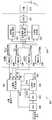
도 3은 종래의 디지털 텔레비전 수신 장치의 블록도이다.3 is a block diagram of a conventional digital television receiver.
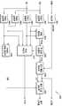
도 4는 본 발명의 일실시예에 따른 동기신호 검출기를 구비하는 디지털 텔레비전 수신 장치의 블록도이다.4 is a block diagram of a digital television receiver having a synchronization signal detector according to an embodiment of the present invention.
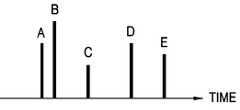
도 5는 시간에 따른 멀티패스 신호들의 크기를 나타내는 일례이다.5 is an example illustrating the magnitudes of multipath signals over time.
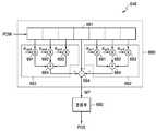
도 6은 본 발명의 일실시예에 따른 동기신호 검출기의 구체적인 블록도이다.6 is a detailed block diagram of a sync signal detector according to an embodiment of the present invention.
도 7은 도 6의 주 경로 검출부의 구체적인 블록도이다.FIG. 7 is a detailed block diagram of the main path detector of FIG. 6.
도 8은 도 6의 동기 신호 검출기의 동작 설명을 위한 흐름도이다.8 is a flowchart for describing an operation of a synchronization signal detector of FIG. 6.
도 9는 본발명의 다른실시예에 따른 동기신호검출기의 구체적인 블록도이다.9 is a detailed block diagram of a synchronization signal detector according to another embodiment of the present invention.
도 10은 도 9의 주 경로 검출부의 구체적인 블록도이다.FIG. 10 is a detailed block diagram of the main path detector of FIG. 9.
도 11은 동기 신호 검출기에서 생성된 동기 신호들의 타이밍도이다.11 is a timing diagram of sync signals generated in a sync signal detector.
본 발명은 디지털 텔레비전(Digital Television)(이하 "DTV"라 약칭함) 수신 장치에 관한 것으로서, 특히 DTV 수신 장치의 동기 신호 검출기에 관한 것이다.BACKGROUND OF THE
최근들어 방송용 시스템들에 급격히 디지털화가 진전되고 있다. 지상파의 경우에 유럽은 OFDM(Orthogonal Frequency Division Multiplexing)에 기반한 DVB-T(Terrestrial Digital Video Broadcasting)로 표준화가 진행되었고, 미국은 잔류 측파대(Vestigial Sideband)(이하 "VSB"라 약칭함) 방식에 기반하여 표준화가 진행되었다. VSB 신호는 ATSC(Advanced Television Subcommittee)에서 규정하고 있다. 특히, 우리나라가 채택한 미국향 DTV 수신 시스템을 위하여, 멀티패스(multi-path) 채널 하에서 잡음이 많이 섞인 VSB 신호를 수신하여 안정적으로 복조 및 디코딩할 수 있는 강건한(robust) 수신 장치가 요구되고 있다.Recently, digitalization is rapidly progressing in broadcasting systems. In the case of terrestrial waves, Europe has standardized on Terrestrial Digital Video Broadcasting (DVB-T) based on Orthogonal Frequency Division Multiplexing (OFDM), while the United States has adopted a residual sideband (hereinafter referred to as "VSB") scheme. Based on the standardization. VSB signals are specified by ATSC (Advanced Television Subcommittee). In particular, for the US DTV reception system adopted by Korea, a robust reception apparatus capable of stably demodulating and decoding received VSB signals mixed with noise under a multi-path channel is required.
VSB 신호 프레임의 구조가 도 1에 도시되어 있다. VSB 신호 프레임은 313 세그먼트(segment)로 각각 구성된 2개의 필드(Odd field(홀수 필드) 및 Even field(짝수 필드))로 이루어져 있다. 각 필드의 첫 세그먼트는 필드 동기 신호(field synchronization signal)가 실리고, 나머지 세그먼트들에는 실제 데이터(Data)와 에러 정정을 위한 에러 정정(FEC:Forward Error Correction) 코드로 구성된 데이터 필드가 실린다. 필드 동기 신호는 도 2와 같은 구조를 가진다. 한 세그먼트는 832 심볼(symbol)을 가지며, 각 세그먼트의 처음 4 심볼 동안에는 도 2에 도시된 바와 같이 세그먼트 동기 신호(segment synchronization signal)가 실린다. VSB 신호는 수신 성능을 높이기 위해서 각 필드 초기에 훈련열(training sequence)을 넣은 데이터 포맷을 가진다. 필드 동기 신호는 511 심볼 길이의 PN(Pseudo-random Number)511 시퀀스, 63 심볼 길이의 PN63 시퀀스와 같이 등화기(equalizer)를 위한 훈련 신호를 가지고 있다. 3 개의 PN 63 시퀀스는 그들의 부호에 따라, 수신되고 있는 신호가 홀수 필드인지 짝수 필드인지를 알려주는 신호이다. 동기 신호 검출기는 PN511 시퀀스를 이용하여 수신 멀티 패스 신호들의 크기와 위치에 대한 프로파일(profile)을 찾아 낼 수 있고, 이에 따라 이러한 프로파일을 이용하여 디코딩 등 시스템 전반에 필요한 동기 신호들을 생성한다.The structure of the VSB signal frame is shown in FIG. The VSB signal frame consists of two fields (Odd field and even field) each composed of 313 segments. The first segment of each field carries a field synchronization signal, and the remaining segments carry a data field composed of actual data and an error correction code for error correction (FEC). The field sync signal has a structure as shown in FIG. One segment has 832 symbols, and a segment synchronization signal is carried during the first four symbols of each segment as shown in FIG. The VSB signal has a data format in which a training sequence is inserted at the beginning of each field to improve reception performance. The field synchronization signal has a training signal for an equalizer such as a Pseudo-random Number (PN) 511 sequence of 511 symbols and a PN63 sequence of 63 symbols in length. The three
종래의 디지털 텔레비전 수신 장치(300)의 블록도가 도 3에 도시되어 있다. 도 3을 참조하면, 종래의 디지털 텔레비전 수신 장치(300)는 튜너(tuner)(310), 복조기(demodulator)(320), 노이즈 제거 필터(NRF:Noise Rejection Filter)(330), 동기 신호 검출기(340), 및 등화기(350)를 구비한다. 상기 복조기(320)는 아날로그-디지털 변환기(ADC:Analog-to-Digital Converter)(321), 필터링 및 다운 샘플링부(filtering and down sampling unit)(322), 심볼 타이밍 복원부(symbol timing recovery unit)(323), 캐리어(carrier) 복원부(324), 및 DC 제거기(DCRM:Direct Current Remover)(329)를 구비하고, 상기 필터링 및 다운 샘플링부(322)는 다위상 필터(PPF:Poly-phase Filter)(325), 5.38MHz 다운 샘플러(down sampler)(326), 정합 필터(MF:Matched Filter)(327), 및 2.69 MHz 소터(sorter)(328)를 구비한다. A block diagram of a conventional
도 3에서, 상기 필터링 및 다운 샘플링부(322)에서 출력된 허수부 신호는 상기 캐리어 복원부(324)로 입력되고, 상기 필터링 및 다운 샘플링부(322)에서 출력 된 실수부 신호는 상기 DC 제거기(329) 및 상기 심볼 타이밍 복원부(323)로 입력된다. 상기 DC 제거기(329)는 상기 필터링 및 다운 샘플링부(322)에서 출력된 실수부 신호에서 DC 성분을 제거한 실수부 신호(RD)를 생성한다. 이에 따라, 상기 종래의 동기신호 검출기(340)는 상기 복조기(320)에서 출력되는 실수부 신호(RD)로부터 상기 PN 시퀀스들에 대한 상관도(correlation) 값들을 계산하여 멀티 패스 신호들의 프로파일을 찾고, 그 중에서 주 경로(main path) 신호를 선택하여, 상기 동기 록킹 제어 신호(LOCK)와 동기 신호들을 생성한다. 필드 동기 신호 및 세그먼트 동기 신호 등이 상기 동기 신호들에 해당한다.In FIG. 3, the imaginary part signal output from the filtering and down
그러나, 종래의 미국향 수신 장치의 동기신호 검출기(340)에서는 자체 판단하에 상기 동기 록킹 제어 신호(LOCK)를 생성한다. 멀티패스 신호들의 위상 옵셋에 의하여 주 경로 신호의 위치는 변할 수 있고, 이와 같은 동적 채널에서 주 경로 신호를 잃게되면 상기 동기 록킹 제어 신호(LOCK)는 디스에이블(disable) 상태로 되어 등화기(350) 동작은 멈춘다. 또한, 종래의 동기신호 검출기(340)에서는 등화기(350) 성능을 고려함이 없이 단순히 멀티 패스 신호들의 프로파일에서 프리고스트(pre-ghost) 위치, 첨두치(peak value) 위치, 또는 포스트고스트(post-ghost) 위치의 중 하나의 신호를 주 경로 신호로 선택한다. 그러나, 등화기(350)는 첨두치 위치의 신호들 좌우 하나의 신호 뿐만아니라, 더 많은 근접 패스들의 신호들에 의하여 많은 영향을 받는다. 따라서, 종래의 동기신호 검출기(340) 동작은 동적 채널에 잘 적응하지 못하여, 시스템 성능을 저하시키는 문제점이 있다.However, the
따라서, 본 발명이 이루고자하는 기술적 과제는 첨두치 위치의 신호들 주변의 근접 패스들의 영향을 고려한 파워 크기를 추정하여 정확한 주 경로를 판단하고, 디코더로부터의 에러값을 동기 록킹 제어 신호 생성에 이용하여 등화기의 안정적인 동작을 보장할 수 있는 디지털 텔레비전 수신 장치의 동기신호 검출기를 제공하는데 있다. Accordingly, the technical problem of the present invention is to estimate the correct main path by estimating the power magnitude considering the influence of the proximity paths around the signals of the peak position, and to use the error value from the decoder to generate the synchronous locking control signal. An object of the present invention is to provide a synchronization signal detector of a digital television receiver capable of ensuring stable operation of an equalizer.
본 발명이 이루고자하는 다른 기술적 과제는 첨두치 위치의 신호들 주변의 근접 패스들 및 디코더로부터의 에러값을 이용한 디지털 텔레비전 수신 장치의 동기 신호 검출 방법을 제공하는데 있다. Another object of the present invention is to provide a synchronization signal detection method of a digital television receiver using proximity paths around signals of a peak position and an error value from a decoder.
상기의 기술적 과제를 달성하기 위한 본 발명의 일면에 따른 동기 신호 검출기는, 위상 계산부, 파워 계산부, 주경로 검출부, 동기 록킹 제어부, 방향 결정부, 동기 신호 생성부, 및 비교부를 구비하는 것을 특징으로 한다. 상기 위상 계산부는 수신 신호로부터의 그 위상과 주 경로 신호의 위상의 차이를 계산하여 상기 위상 차이를 상기 수신 신호의 위상 옵셋값으로서 생성한다. 상기 파워 계산부는 상기 수신 신호로부터 파워 크기를 계산한다. 상기 주경로 검출부는 상기 파워 크기로부터 상기 주 경로 신호를 생성한다. 상기 동기 록킹 제어부는 상기 주 경로 신호를 카운트하여 동기 록킹 제어 신호 및 카운트 정보 신호를 생성한다. 상기 방향 결정부는 상기 수신 신호로부터 필드 방향 신호를 생성한다. 상기 동기 신호 생성부는 상기 동기 록킹 제어 신호, 상기 카운트 정보 신호, 및 상기 필드 방향 신호를 이용하여, 상기 수신 신호의 세그먼트 동기 신호 및 상기 세그먼트 동기 신호에 동기 된 다수의 동기 신호들을 생성한다. 상기 비교부는 수신되는 에러값을 소정시간 동안 누적한 값이 임계치보다 작은가를 알리는 록킹 해제 제어 신호를 생성한다. 여기서, 상기 동기 록킹 제어부는 상기 록킹 해제 제어 신호에 따라 상기 동기 록킹 제어 신호의 논리 상태를 결정하는 것을 특징으로 한다.According to an aspect of the present invention, a sync signal detector includes a phase calculator, a power calculator, a main path detector, a sync locking controller, a direction determiner, a sync signal generator, and a comparator. It features. The phase calculator calculates the difference between the phase from the received signal and the phase of the main path signal and generates the phase difference as a phase offset value of the received signal. The power calculator calculates a power level from the received signal. The main path detector generates the main path signal from the power magnitude. The synchronous locking control unit counts the main path signal to generate a synchronous locking control signal and a count information signal. The direction determiner generates a field direction signal from the received signal. The sync signal generator generates a plurality of sync signals synchronized with the segment sync signal of the received signal and the segment sync signal by using the sync locking control signal, the count information signal, and the field direction signal. The comparator generates a unlocking control signal indicating whether the accumulated value of the received error value for a predetermined time is smaller than the threshold value. Here, the synchronous locking control unit may determine a logical state of the synchronous locking control signal according to the unlocking control signal.
상기의 기술적 과제를 달성하기 위한 본 발명의 다른 일면에 따른 디지털 텔레비전 수신 장치는, 복조기, 동기 신호 검출기, 위상 보상기, 등화기 및 디코더를 구비하는 것을 특징으로 한다. 상기 복조기는 튜너에서 추출된 아날로그 VSB 신호를 디지털 신호로 변환하고, 상기 디지털 신호를 복조하여 실수부 신호 및 허수부 신호를 생성한다. 상기 동기 신호 검출기는 상기 실수부 신호와 허수부 신호를 이용하여 그들의 상관도 값들로부터 주 경로 신호 및 필드 방향 신호를 추정하고, 상기 추정된 주경로 신호 및 필드 방향 신호에 따라 상기 VSB 신호의 위상 옵셋값, 세그먼트 동기 신호, 및 상기 세그먼트 동기 신호에 동기된 다수의 동기 신호들을 생성한다. 상기 위상 보상기는 상기 위상 옵셋값에 따라 상기 실수부 신호의 위상을 보상하여 출력한다. 상기 등화기는 상기 위상 보상기의 출력 신호를 왜곡 보상 필터링하여 출력한다. 상기 디코더는 상기 등화기 출력 신호에 대한 에러 정정을 수행하고, 상기 에러 정정 과정에서 계산된 에러값을 출력한다. 여기서, 상기 동기 신호 검출기는 상기 에러값을 이용하여 록킹 해제 제어 신호를 생성하고, 상기 록킹 해제 제어 신호에 따라 상기 동기 신호들의 록킹이 결정되는 것을 특징으로 한다.According to another aspect of the present invention, a digital television receiver includes a demodulator, a synchronous signal detector, a phase compensator, an equalizer, and a decoder. The demodulator converts the analog VSB signal extracted from the tuner into a digital signal and demodulates the digital signal to generate a real part signal and an imaginary part signal. The synchronization signal detector estimates a main path signal and a field direction signal from their correlation values using the real part signal and the imaginary part signal, and phase offset of the VSB signal according to the estimated main path signal and field direction signal. Generate a value, a segment sync signal, and a plurality of sync signals synchronized with the segment sync signal. The phase compensator compensates and outputs a phase of the real part signal according to the phase offset value. The equalizer outputs the distortion compensation filtering of the output signal of the phase compensator. The decoder performs error correction on the equalizer output signal and outputs an error value calculated in the error correction process. Here, the sync signal detector generates the unlock control signal using the error value, and the locking of the sync signals is determined according to the unlock control signal.
상기의 다른 기술적 과제를 달성하기 위한 본 발명의 일면에 따른 디지털 텔 레비전 수신 장치의 동기 신호 검출 방법은, 수신 신호로부터의 그 위상과 주 경로 신호의 위상의 차이를 계산하여 상기 위상 차이를 상기 수신 신호의 위상 옵셋값으로서 생성하는 단계; 상기 수신 신호로부터 파워 크기를 계산하는 단계; 상기 파워 크기로부터 상기 주 경로 신호를 생성하는 단계; 상기 주 경로 신호를 카운트하여 동기 록킹 제어 신호 및 카운트 정보 신호를 생성하는 단계; 상기 수신 신호로부터 필드 방향 신호를 생성하는 단계; 및 상기 동기 록킹 제어 신호, 상기 카운트 정보 신호, 및 상기 필드 방향 신호를 이용하여, 상기 수신 신호의 세그먼트 동기 신호 및 상기 세그먼트 동기 신호에 동기된 다수의 동기 신호들을 생성하는 단계; 수신되는 에러값을 소정시간 동안 누적한 값이 임계치보다 작은가를 알리는 록킹 해제 제어 신호를 생성하는 단계; 및 상기 록킹 해제 제어 신호에 따라 상기 동기 록킹 제어 신호의 논리 상태를 결정하는 단계를 구비하는 것을 특징으로 한다.According to another aspect of the present invention, there is provided a synchronization signal detecting method of a digital television receiver, wherein the phase difference from a received signal and a phase of a main path signal are calculated to receive the phase difference. Generating as a phase offset value of the signal; Calculating a power magnitude from the received signal; Generating the main path signal from the power magnitude; Counting the main path signal to generate a synchronous locking control signal and a count information signal; Generating a field direction signal from the received signal; And generating a plurality of synchronization signals synchronized with the segment synchronization signal of the received signal and the segment synchronization signal by using the synchronization locking control signal, the count information signal, and the field direction signal. Generating a unlocking control signal indicating whether a value accumulated in a received error value for a predetermined time is smaller than a threshold value; And determining a logic state of the synchronous locking control signal according to the unlocking control signal.
상기의 다른 기술적 과제를 달성하기 위한 본 발명의 다른 일면에 따른 디지털 텔레비전 수신 방법은, 튜너에서 추출된 아날로그 VSB 신호를 디지털 신호로 변환하는 단계; 상기 디지털 신호를 복조하여 실수부 신호 및 허수부 신호를 생성하는 단계; 상기 실수부 신호와 허수부 신호를 이용하여 그들의 상관도 값들로부터 주 경로 신호 및 필드 방향 신호를 추정하는 단계; 상기 추정된 주경로 신호 및 필드 방향 신호에 따라 상기 VSB 신호의 위상 옵셋값, 세그먼트 동기 신호, 및 상기 세그먼트 동기 신호에 동기된 다수의 동기 신호들을 생성하는 단계; 상기 위상 옵셋값에 따라 상기 실수부 신호의 위상을 보상하여 출력하는 단계; 상기 위상 보상된 신호를 왜곡 보상 필터링하여 출력하는 단계; 상기 필터링된 신호에 대한 에러 정정을 수행하고, 상기 에러 정정 과정에서 계산된 에러값을 출력하는 단계; 및 상기 에러값을 이용하여 록킹 해제 제어 신호를 생성하는 단계를 구비하고, 상기 록킹 해제 제어 신호에 따라 상기 동기 신호들의 록킹이 결정되는 것을 특징으로 한다.According to another aspect of the present invention, there is provided a digital television receiving method comprising: converting an analog VSB signal extracted from a tuner into a digital signal; Demodulating the digital signal to generate a real part signal and an imaginary part signal; Estimating a main path signal and a field direction signal from their correlation values using the real part signal and the imaginary part signal; Generating a phase offset value of the VSB signal, a segment synchronization signal, and a plurality of synchronization signals synchronized with the segment synchronization signal according to the estimated main path signal and the field direction signal; Compensating and outputting a phase of the real part signal according to the phase offset value; Distortion-compensated filtering and outputting the phase-compensated signal; Performing error correction on the filtered signal and outputting an error value calculated in the error correction process; And generating a unlocking control signal using the error value, wherein locking of the synchronization signals is determined according to the unlocking control signal.
본 발명과 본 발명의 동작상의 이점 및 본 발명의 실시에 의하여 달성되는 목적을 충분히 이해하기 위해서는 본 발명의 바람직한 실시예를 예시하는 첨부 도면 및 도면에 기재된 내용을 참조하여야 한다.DETAILED DESCRIPTION In order to fully understand the present invention, the operational advantages of the present invention, and the objects achieved by the practice of the present invention, reference should be made to the accompanying drawings which illustrate preferred embodiments of the present invention and the contents described in the drawings.
이하, 첨부한 도면을 참조하여 본 발명의 바람직한 실시예를 설명함으로써, 본 발명을 상세히 설명한다. 각 도면에 제시된 동일한 참조부호는 동일한 부재를 나타낸다.Hereinafter, exemplary embodiments of the present invention will be described in detail with reference to the accompanying drawings. Like reference numerals in the drawings denote like elements.
본 발명의 일실시예에 따른 동기신호 검출기(440)를 구비하는 디지털 텔레비전 수신 장치(400)가 도 4에 도시되어 있다. 도 4를 참조하면, 상기 디지털 텔레비전 수신 장치(400)는, 튜너(tuner)(410), 복조기(demodulator)(420), 위상 보상기(430), 동기 신호 검출기(440), 등화기(equalizer)(450), 및 디코더(decoder)(460)를 구비한다.4 illustrates a
상기 튜너(410)는 공중 매체로 전송된 고주파 VSB 신호를 안테나를 통하여 수신하고, 수신 신호에 대하여 할당된 채널 튜닝을 수행하여 기저 대역(baseband)의 아날로그 VSB 신호를 추출하여 출력한다.The
상기 복조기(420)는 아날로그-디지털 변환기(ADC:Analog-to-Digital Converter)(421), 필터링 및 다운 샘플링부(filtering and down sampling unit)(422), 심볼 타이밍 복원부(symbol timing recovery unit)(423), 캐리어(carrier) 복원부(424), 제1 DC 제거기(DCRM:Direct Current Remover)(425), 제2 DC 제거기(426), 제3 DC 제거기(427) 및 제2 DC 제거기(428)를 구비하고, 상기 필터링 및 다운 샘플링부(422)는 도 3의 필터링 및 다운 샘플링부(322)와 유사하다. 상기 아날로그-디지털 변환기(421)는 상기 튜너(410)에서 추출된 아날로그 VSB 신호를 디지털 신호로 변환한다. 이에 따라, 상기 변환된 디지털 신호는 상기 필터링 및 다운 샘플링부(422), 상기 심볼 타이밍 복원부(423), 및 상기 캐리어 복원부(424)에 의하여 소정 방식에 따라 복조된다. 상기 필터링 및 다운 샘플링부(422)에서는 QAM(Quadrature Amplitude Modulation) 포맷, BPSK(Binary Phase-Shift Keying) 포맷, 또는 QPSK(Quadrature Phase-Shift Keying) 포맷 등 그 다양한 복조 형태에 따라, 심볼 레이트(rate)에 비례하는 레이트의 신호를 샘플링하여 출력하기 위한 다운 샘플링을 수행한다. 이외에도, 상기 필터링 및 다운 샘플링부(422)는 상기 아날로그-디지털 변환기(421)에서 생성된 디지털 VSB 신호를 다위상 필터링 및 정합 필터링 처리하여 복조된 상기 복소 신호들(complex signals)을 생성한다.The
상기 다운 샘플링에 의하여 일반적으로는, 제1 복소 신호, 즉, 소정 샘플 타임 T(sec)마다 샘플된 실수부(real component) 신호와 상기 T마다 샘플된 허수부 신호가 생성된다. 이와 같이 생성된 상기 T 샘플 타임마다 샘플된 실수부 신호는 상기 제1 DC 제거기(425)에 의하여 DC 성분이 제거된 제1 실수부 신호(RD)로 출력되고, 상기 T 샘플 타임마다 샘플된 허수부 신호는 상기 제3 DC 제거기(427)에 의하여 DC 성분이 제거된 제1 허수부 신호(ID)로 출력된다. 이와 같은 상기 제1 실수 부 신호(RD)와 상기 제1 허수부 신호(ID)를 이용하여 동기 신호들을 검출하는 본 발명의 일실시예에 따른 동기 신호 검출기가 도 6에서 설명된다.In general, the down sampling generates a first complex signal, that is, a real component signal sampled every predetermined sample time T (sec) and an imaginary part signal sampled for each T. The real part signal sampled for each T sample time generated as described above is output as a first real part signal RD from which a DC component is removed by the
특히, 본 발명에서는 상기 다운 샘플링에 의하여 제2 복소 신호, 즉, 상기 제1 복소 신호를 T/2 지연시킨 신호가 상기 T 샘플 타임마다 샘플된 실수부 신호, 및 허수부(imaginary component) 신호를 더 생성하는 복조기(420)에 대하여도 적용되는 동기 신호 검출기를 제안한다. 상기 T/2 지연되어 샘플된 실수부 신호는 상기 제2 DC 제거기(426)에 의하여 DC 성분이 제거된 제2 실수부 신호(SH_RD)로 출력되고, 상기 T/2 지연되어 샘플된 허수부 신호는 상기 제4 DC 제거기(428)에 의하여 DC 성분이 제거된 제2 허수부 신호(SH_ID)로 출력된다. 상기 제1 실수부 신호(RD)와 상기 제1 허수부 신호(ID), 및 상기 제2 실수부 신호(SH_RD)와 상기 제2 허수부 신호(SH_ID)를 이용하여 동기 신호들을 검출하는 본 발명의 다른 실시예에 따른 동기 신호 검출기가 도 9에서 설명된다.Particularly, in the present invention, a second complex signal, ie, a signal obtained by delaying the first complex signal by T / 2 by the down sampling, is a real part signal and an imaginary component signal sampled every T sample time. We propose a synchronization signal detector that is also applied to the
한편, 수신된 멀티패스 신호들의 시간에 따른 크기를 나타내는 일례가 도 5에 도시되어 있다. 예를 들어, 상기 복조기(420)의 출력 신호들(RD, SH_RD, ID, SH_ID)도 도 5와 같은 멀티 패스 신호들의 프로파일을 가질 수 있다. 도 5와 같이, 수신된 멀티패스 신호들의 전력량을 이용하여 매인 패스를 결정할 경우에, A 및 B 와 같이 인접한 패스들은 서로 영향을 미쳐 전력량이 커지는 것을 볼 수 있다. 즉, A에서는 B 의 영향으로 전력량이 많이 커지고, B에서는 A 의 영향으로 전력량이 조금 커지게 되며, 이에 따라 A 와 B 간 전력량 차이가 줄어들 뿐만 아니라 다른 패스들(C~E)에 비해 A 및 B 의 전력량은 커지므로 메인 패스 선택시 영향을 받는다.On the other hand, an example showing the magnitude over time of the received multipath signals is shown in FIG. For example, the output signals RD, SH_RD, ID, and SH_ID of the
또한, 동적 채널인 경우에서 위상과 멀티패스의 형태가 복잡하게 바뀌게 될 때, 종래의 동기신호 검출기(340)는 동적 채널에서 위상 옵셋에 취약하게 되어, 검출된 주 경로 신호의 위치가 달라짐을 판단하지 못하고, 동기 록킹 제어 신호(LOCK)를 디스에이블(disable) 상태로 만들어 등화기 동작을 멈추게한다. 그리고, 종래의 동기신호 검출기(340)는 등화기(350) 성능을 고려함이 없이 단순히 멀티 패스 신호들의 프로파일에서 첨두치 위치의 신호(B)를 주 경로 신호로 선택한다. 이와 같은 종래의 동기신호 검출기(340)의 동작은 등화기의 수렴 속도와 성능에 영향을 미쳐 결국 성능 열화로 나타난다.In addition, when the shape of the phase and the multipath is complicated in the case of the dynamic channel, the conventional
그러나, 상기 동기 신호 검출기(440)는 실수부 신호들(RD/SH_RD)과 허수부 신호들(ID/SH_ID)로부터 그들의 PN511 및 PN63 상관도 값들을 이용하여 파워 크기(POW) 및 필드 방향 신호(DIR)를 추정한다. 상기 추정된 파워 크기(POW)는 첨두치 위치의 신호들 주변의 근접 패스들의 영향을 반영한 정확한 주 경로 신호(POS) 추정에 이용되고, 상기 주경로 신호(POS) 위치의 실수부 신호와 허수부 신호 각각의 PN511 및 PN63 상관도 값들이 위상 옵셋값(PHV) 추정에 이용된다. 또한, 상기 동기 신호 검출기(440)는 상기 주경로 신호(POS) 및 상기 필드 방향 신호(DIR)를 기반으로 상기 VSB 신호의 세그먼트 동기 신호(SEG_SYNC), 및 상기 세그먼트 동기 신호(SEG_SYNC)에 동기된 다수의 동기 신호들(도 11 참조)을 생성한다. 상기 동기 신호들은 디코딩 등 시스템 전반에 이용된다. 그리고, 상기 동기 신호 검출기(440)가 상기 에러값(ERR)을 기반으로 생성하는 동기 록킹(locking) 제어 신호(LOCK)에 따라 상기 등화기(450)의 동작이 온(on) 또는 오프(off) 될 수 있다. 이는 동적 채 널에서 등화기(450)의 안정적인 동작을 보장한다. 상기 동기 신호 검출기(440)에 대해서는 도 6 내지 도 10의 설명에서 좀더 자세히 기술된다.However, the
도 6의 동기 신호 검출기(440)가 적용되는 경우에는, 상기 위상 보상기(430)는 상기 제1 실수부 신호(RD)를 수신하여, 상기 위상 옵셋값(PHV)에 따라 상기 수신된 신호의 위상 옵셋(offset)을 제거하여 출력한다. 도 9의 동기 신호 검출기(440)가 적용되는 경우에는, 상기 위상 보상기(430)는 상기 제1 실수부 신호(RD) 또는 상기 제2 실수부 신호(SH_RD) 중 어느 하나를 수신하여, 상기 위상 옵셋값(PHV)에 따라 상기 수신된 신호의 위상 옵셋(offset)을 제거하여 출력한다. 여기서, 상기 위상 보상기(430)에 입력되는 상기 제1 실수부 신호(RD) 또는 상기 제2 실수부 신호(SH_RD) 중 어느 하나는 상기 동기 신호 검출기(440)에서 선택된다. When the
상기 등화기(450)는 FIR(Finite Impulse Response) 필터링 방식에 의하여 상기 위상 보상기(430)의 출력 신호를 필터링하며, 상기 등화기(450)로서 단순 FIR 방식을 개선한 DFE(Decision Feedback Equalizer) 구조가 적용될 수도 있다. 상기 등화기(450)의 출력은 RS(Reed Solomon) 디코더(460) 또는 비터비(Viterbi) 디코더 등으로 입력되고, 이에 따라 에러 정정(예를 들어, FEC:Forward Error Correction) 및 디코딩 처리되어 디스플레이 및 오디오 등을 위한 신호들이 생성된다. 상기 디코더(460)에서는 에러 정정 알고리즘에 따른 에러 정정 과정에서 계산된 패킷(packet) 에러값(ERR)을 상기 동기 신호 검출기(440)로 출력한다.The
도 6은 본 발명의 일실시예에 따른 동기 신호 검출기(440)의 구체적인 블록도이다. 도 6을 참조하면, 상기 동기 신호 검출기(440)는 제1 PN511 상관부(641), 제2 PN511 상관부(642), 제1 PN63 상관부(643), 제2 PN63 상관부(644), 파워 계산부(645), 주경로 검출부(646), 위상 계산부(647), PN63 결정부(648), 동기 록킹 제어부(synchronization locking control unit)(649), 및 동기 신호 생성부(650)를 구비한다. 도 6의 동기 신호 검출기(440)의 동작 설명을 위하여 도 8의 흐름도가 참조된다.6 is a detailed block diagram of a
먼저, 상기 동기 신호 검출기(440)는 도 4의 복조기(420)로부터 생성된 상기 제1 복소 신호를 이루는 상기 제1 실수부 신호(RD)와 상기 제1 허수부 신호(ID)를 수신한다(도 8의 S810). 이에 따라 상기 제1 PN511 상관부(641), 및 상기 제2 PN511 상관부(642) 각각은 상기 실수부 신호(RD)와 상기 허수부 신호(ID)에 대한 PN511 시퀀스 상관을 수행하고, 상기 제1 PN63 상관부(643) 및 상기 제2 PN63 상관부(644) 각각은 상기 실수부 신호(RD)와 상기 허수부 신호(ID)에 대한 PN63 시퀀스 상관을 수행하여 해당 상관값들을 출력한다(도 8의 S820).First, the
상기 PN511 시퀀스 상관은 도 2의 PN511 훈련열(training sequence)에 따른 필드 초기를 발견하기 위하여 이루어진다. 상기 제1 PN511 상관부(641) 및 상기 제2 PN511 상관부(642) 각각에 입력되는 상기 제1 실수부 신호(RD)와 상기 제1 허수부 신호(ID)는, 내부에서 소정 샘플 단위로 지연되고, 지연된 다수 비트의 신호들 각각에 대응되어 있는 소정 레지스터 값들과 승산되며, 승산된 값들이 모두 합산된 값은 상기 PN511 시퀀스 상관에 의한 상관도 값들이 된다. 상기 소정 레지스터(미도시)에는 PN511 심볼들에 대한 상관 계수들이 저장되어 있다. 이와 같이 상관도 값의 계산에 대해서는 이 분야에서 통상의 지식을 가진 자라면 잘 이해할 수 있다.The PN511 sequence correlation is performed to find the initial field according to the PN511 training sequence of FIG. 2. The first real part signal RD and the first imaginary part signal ID input to each of the
상기 PN63 시퀀스 상관은 도 2의 PN63 훈련열(training sequence)에 따른 필드 방향(홀수 필드 또는 짝수 필드)을 발견하기 위하여 이루어진다. 상기 제1 PN63 상관부(643) 및 상기 제2 PN63 상관부(644) 각각에 입력되는 상기 제1 허수부 신호(ID)와 상기 제1 실수부 신호(RD)는, 내부에서 소정 샘플 단위로 지연되고, 지연된 다수 비트의 신호들 각각에 대응되어 있는 소정 레지스터 값들과 승산되며, 승산된 값들이 모두 합산된 값은 상기 PN63 시퀀스 상관에 의한 PN63 상관도 값들이 된다. 상기 소정 레지스터(미도시)에는 PN63 심볼들에 대한 상관 계수들이 저장되어 있다.The PN63 sequence correlation is made to find the field direction (odd field or even field) according to the PN63 training sequence of FIG. 2. The first imaginary part signal ID and the first real part signal RD, which are input to each of the
이에 따라, 상기 파워 계산부(645)는 상기 제1 실수부 신호(RD) 및 상기 제1 허수부 신호(ID)에 대한 상기 PN511 상관도 값들로부터 파워 크기(POW)를 계산한다(도 8의 S830). 파워 크기의 계산은 실수부 신호의 자승값과 허수부 신호의 자승값을 합산한 값으로 할 수 있다.Accordingly, the
상기 주경로 검출부(646)의 구체적인 블록도가 도 7에 도시되어 있다. 도 7을 참조하면, 상기 주경로 검출부(646)는 근접 패스 반영부(multi-path reflection unit)(660), 및 결정부(680)를 구비한다.A detailed block diagram of the
상기 근접 패스 반영부(660)는 다수의 지연 수단들(661), 제1 계수 처리부(662), 제2 계수 처리부(663), 및 감산부(664)를 구비한다. 상기 다수의 지연 수단들(661)은 상기 파워 계산부(645)에서 입력되는 상기 파워 크기(POW)를 소정 샘플 시간 단위로 지연시켜서 서로 샘플 시간만큼 시간차를 가지는 다수의 지연 파워 크기들을 생성한다. 상기 제1 계수 처리부(662)는 다수의 승산기들(681~683) 및 합산 기(684)를 구비하여, 프리 고스트들(pre-ghost)과 승산을 위한 계수들(Kpr1~Kpr3) 각각을 상기 지연 파워 크기들 중 해당 지연 파워 크기와 승산하고, 승산된 값들을 합산하여 출력한다. 상기 제2 계수 처리부(663)는 다수의 승산기들(691~693) 및 합산기(694)를 구비하여, 포스트 고스트들(post-ghost)과 승산을 위한 계수들(Kpo1~Kpo3) 각각을 상기 지연 파워 크기들 중 해당 지연 파워 크기와 승산하고, 승산된 값들을 합산하여 출력한다. 이에 따라, 상기 감산부(664)는 상기 지연 파워 크기들 중 중앙값에서, 상기 합산기들(684, 694)에서 출력되는 값들을 감산하여 그 결과를 결정 신호(WP)로서 출력한다. 도 7에서, 상기 결정부(680)는 상기 결정 신호(WP)가 임계치보다 크면, 그 때의 값을 상기 주 경로 신호(POS)로서 결정한다.The proximity path reflector 660 includes a plurality of delay means 661, a
상기 근접 패스 반영부(660)에 이용된 상기 승산 계수들(Kpr1~Kpr3, Kpo1~Kpo3)은 등화기(450)의 성능을 고려하여 적당히 정해질 수 있다. 즉, 상기 승산 계수들의 설정에 의하여, 상기 결정부(680)는 한 필드(field) 내의 상기 파워 크기들(POW)로부터 최대값 위치(예를 들어, 도 5의 B)의 값을 상기 주 경로 신호(POS)로서 생성할 수 있다. 또는, 상기 결정부(660)는 한 심볼 내의 상기 파워 크기들(POW)로부터 최대값(예를 들어, 도 5의 B) 이전의 프리 고스트(pre-ghost) 파워 크기들(예를 들어, 도 5의 A) 중 어느 하나의 위치의 값을 상기 주 경로 신호(POS)로서 생성할 수 있다. 이외에도, 상기 결정부(660)는 상기 최대값 이후의 포스트 고스트(post-ghost) 파워 크기들(예를 들어, 도 5의 C~E)중 어느 하나, 또는 인접 패스에 영향을 받지 않는 패스들(예를 들어, 도 5의 C~E)중 가장 큰 패스(예를 들어, 도 5의 D)의 위치의 값을 상기 주 경로 신호(POS)로서 생성할 수 있다.The multiplication coefficients Kpr1 to Kpr3 and Kpo1 to Kpo3 used in the proximity
이때, 상기 동기 록킹 제어부(649)는 여러 필드 동안 상기 주 경로 신호(POS)의 위치값이 같은 경우를 카운트하고, 그 카운트 값과 임계치를 비교하여 동기 록킹 제어 신호(LOCK) 및 카운트 정보 신호(CV)를 생성한다. 상기 동기 록킹 제어 신호(LOCK)는, 상기 주 경로 신호(POS)의 위치 카운트 값이 동기 신호들의 록킹을 위한 임계치보다 클 경우 논리 하이 상태이고, 상기 주 경로 신호(POS)의 위치 카운트 값이 동기 신호들을 록킹하지 않기 위한 임계치보다 작을 경우 논리 로우 상태로 될 수 있다. 상기 카운트 정보 신호(CV)는 심볼 수를 알려주는 심볼 카운트 신호 및 세그먼트 수를 알려주는 세그먼트 카운트 신호를 포함한다. 즉, 심볼 카운트 신호는 심볼 기간 마다 임펄스 형태로 나타나는 상기 주 경로 신호(POS)를 카운트한 신호이고, 상기 세그먼트 카운트 신호는 심볼 카운트 신호를 카운트하여 한 세그먼트, 즉, 832 심볼 기간 마다 일씩 증가시킨 신호이다. 상기 카운트 정보 신호(CV)는 프레임 단위로 리셋(reset)될 수 있다.In this case, the synchronous
그러나, 상기 동기 록킹 제어부(649)에서의 상기 동기 록킹 제어 신호(LOCK)의 생성은 상기 비교부(651)의 제어를 받는다. 즉, 상기 비교부(651)는 상기 디코더(460)로부터 받는 에러값(ERR)을 소정시간 동안 누적한 값이 임계치보다 작은가를 알리는 록킹 해제 제어 신호(UNCON)를 생성하고, 이에 따라, 상기 동기 록킹 제어부(649)는 상기 록킹 해제 제어 신호(UNCON)에 따라 상기 동기 록킹 제어 신호(LOCK)의 논리 상태를 결정한다(도 8의 S850). 예를 들어, 상기 디코더(460)에서 출력된 일정 레벨 이상의 상기 에러값(ERR)이 계속하여 출력될 때, 이를 소정 심볼 기간 동안 누적한 값이 임계치보다 작으면, 상기 록킹 해제 제어 신호(UNCON)는 논 리 로우 상태로되고, 이에 따라 상기 동기 록킹 제어 신호(LOCK)는 논리 하이 상태로 된다. 또한, 상기 소정 심볼 기간 동안 누적한 에러값이 임계치보다 크면, 상기 록킹 해제 제어 신호(UNCON)는 논리 하이 상태로 되고, 이에 따라 상기 동기 록킹 제어 신호(LOCK)는 논리 로우 상태로된다.However, generation of the synchronous locking control signal LOCK by the
상기 동기 록킹 제어 신호(LOCK)에 따라 상기 동기 신호 생성부(650)의 동작이 온 또는 오프되고, 또한 도 4의 상기 위상 보상기(430) 및 상기 등화기(450)의 동작이 온 또는 오프될 수 있다. 예를 들어, 상기 동기 록킹 제어 신호(LOCK)가 로직 하이(high) 상태일 경우에는, 동기 신호들이 록킹되고, 상기 동기 신호 생성부(502), 상기 위상 보상기(430) 및 상기 등화기(450)가 동작한다(도 8의 S870). 그러나, 상기 록킹 해제 제어 신호(UNCON)가 논리 하이 상태일 경우에는, 상기 동기 록킹 제어 신호(LOCK)가 로직 로우(low) 상태로 되고, 이에 따라 동기 신호들의 록킹 상태가 해제(unlocking)되고, 상기 동기 신호 생성부(650), 상기 위상 보상기(430) 및 상기 등화기(450)가 동작하지 않는다(도 8의 S860).The operation of the
한편, 상기 위상 계산부(501)는 상기 제1 PN511 상관부(641) 및 상기 제2 PN511 상관부(642)에서 출력된 상기 제1 복소 신호(RD, ID)에 대한 PN511 상관도 값들을 이용하여 상기 수신 VSB 신호의 위상을 계산하고, 상기 계산된 VSB 신호의 위상과 상기 주 경로 신호(POS)의 위상의 차이를 계산하여 상기 위상 차이를 위상 옵셋값(PHV)으로서 생성한다(도 8의 S880). 이에 따라, 도 4의 상기 위상 보상기(430)는 상기 상기 제1 복소 신호(RD, ID) 중 상기 제1 실수부 신호(RD)를 수신하여, 상기 위상 옵셋값(PHV)에 따라 상기 선택된 실수부 신호의 위상 옵셋을 제거하 여 출력한다(도 8의 S890). 도 6에 도시된 바와 같이, 상기 위상 계산부(501)는 더 정확한 위상 계산을 위하여, 상기 제1 PN63 상관부(643) 및 상기 제2 PN63 상관부(644)에서 출력된 상기 제1 복소 신호(RD, ID)에 대한 PN63 상관도 값들을 더 이용하여 상기 수신 VSB 신호의 위상을 계산할 수도 있다.Meanwhile, the
상기 PN63 결정부(648)는 상기 제1 PN63 상관부(643) 및 상기 제2 PN63 상관부(644) 각각으로부터 생성된 상기 수신 VSB 신호의 실수부 신호(RD) 및 허수부 신호(ID) 각각에 대한 상기 PN63 상관도 값들로부터 필드 방향 신호(DIR)를 생성한다. 예를 들어, 상기 PN63 상관도 값들이 홀수 필드(odd field)에 해당하는 값들을 가지는 경우에 상기 필드 방향 신호(DIR)는 로직 하이 상태이고, 상기 PN63 상관도 값들이 짝수 필드(even field)에 해당하는 값들을 가지는 경우에 상기 필드 방향 신호(DIR)는 로직 로우 상태일 수 있다.The
이에 따라, 상기 동기 신호 생성부(650)는 상기 동기 록킹 제어부(649)에서 생성된 상기 동기 록킹 제어 신호(LOCK) 및 상기 카운트 정보 신호(CV)와 상기 PN63 결정부(648)에서 생성된 상기 필드 방향 신호(DIR)를 이용하여, 동기 신호들을 생성한다(도 8의 S900). 이와 같이 비교부(651)가 디코더(460)로부터 받는 에러값(ERR)을 체크하고, 상기 동기 신호 생성부(650)가 동기 신호들을 생성하는 과정(도 8의 S850~S900)은 반복된다. 상기 카운트 정보 신호(CV)는 심볼 수를 알려주는 심볼 카운트 신호 및 세그먼트 수를 알려주는 세그먼트 카운트 신호를 포함한다. 상기 동기 신호 검출기(440)에서 생성된 동기 신호들이 도 11에 도시되어 있다. 도 11을 참조하면, 상기 동기 신호 생성부(503)가 생성하는 동기 신호들은, 세그먼트 동기 신호(SEG_SYNC), 필드 동기 신호(FIELD_1), 313 세그먼트 동기 신호(FIELD_313s), 704 심볼 동기 신호(FIELD_704), 832 심볼 동기 신호(FIELD_832), 및 511 심볼 동기 신호(FIELD_511)를 포함한다. 이와 같은 동기 신호들은 모두 세그먼트 동기 신호(SEG_SYNC)에 동기되어 있다. 상기 세그먼트 동기 신호(SEG_SYNC)는 한 세그먼트 기간 마다 1 심볼 기간 동안 로직 하이 상태이다. 상기 필드 동기 신호(FIELD_1)는 한 필드 기간 마다 1 심볼 기간 동안 로직 하이 상태이다. 상기 313 세그먼트 동기 신호(FIELD_313s)는 313 세그먼트, 즉, 한 필드 기간 동안 로직 하이 상태 또는 로직 로우 상태를 번갈아 유지한다. 상기 704 심볼 동기 신호(FIELD_704)는 한 필드 기간 중에서 도 2의 세그먼트 동기를 위한 4 심볼, PN511 시퀀스를 위한 511 심볼, 및 3개의 PN 63 시퀀스를 위한 189 심볼, 즉, 704 심볼 동안 로직 하이 상태이다. 상기 832 심볼 동기 신호(FIELD_832)는 한 필드 기간 중에서 832 심볼, 즉, 한 세그먼트 기간 동안 로직 하이 상태이다. 상기 511 심볼 동기 신호(FIELD_511)는 PN511 시퀀스 시작 시점부터 PN511 시퀀스 종료점 까지 로직 하이 상태이다.Accordingly, the
도 9는 본 발명의 다른 실시예에 따른 동기 신호 검출기(440)의 구체적인 블록도이다. 도 9를 참조하면, 상기 동기 신호 검출기(440)는 제1 PN511 상관부(441), 제2 PN511 상관부(442), 제3 PN511 상관부(443), 제4 PN511 상관부(444), 제1 파워 계산부(445), 제2 파워 계산부(446), 주경로 검출부(447), 데이터 선택부(448), 제1 PN63 상관부(449), 제2 PN63 상관부(500), PN63 방향 결정부(505), 위상 계산부(501), 동기 록킹 제어부(synchronization locking control unit)(502), 및 동기 신호 생성부(503)을 구비한다. 도 9의 동기 신호 검출기(440)의 동작 설명을 위하여 도 8의 흐름도가 다시 참조된다.9 is a detailed block diagram of a
먼저, 상기 동기 신호 검출기(440)는 도 4의 복조기(420)로부터 상기 제1 실수부 신호(RD)와 상기 제1 허수부 신호(ID)로 이루어진 제1 복소 신호와, 상기 제2 실수부 신호(SH_RD)와 상기 제2 허수부 신호(SH_ID)로 이루어진 제2 복소 신호를 수신한다(도 8의 S810). 이에 따라 상기 제1 PN511 상관부(441), 상기 제2 PN511 상관부(443), 상기 제3 PN511 상관부(443), 및 상기 제4 PN511 상관부(444) 각각은 상기 해당 입력 신호에 대한 PN511 시퀀스 상관을 수행하여 해당 상관값들(C1~C4)을 출력한다(도 8의 S820).First, the
이에 따라, 상기 제1 파워 계산부(445)는 상기 제1 복소 신호를 이루는 상기 제1 실수부 신호(RD) 및 상기 제1 허수부 신호(ID)에 대한 상기 PN511 상관도 값들(C1, C2)로부터 제1 파워 크기(POW1)를 계산한다(도 8의 S830). 또한, 상기 제2 파워 계산부(446)는 상기 제2 복소 신호를 이루는 상기 제2 실수부 신호(SH_RD) 및 상기 제2 허수부 신호(SH_ID)에 대한 상기 PN511 상관도 값들(C3, C4)로부터 제2 파워 크기(POW2)를 계산한다(도 8의 S830). 파워 크기의 계산은 실수부 신호의 자승값과 허수부 신호의 자승값을 합산한 값으로 할 수 있다.Accordingly, the
상기 주경로 검출부(447)의 구체적인 블록도가 도 10에 도시되어 있다. 도 10을 참조하면, 상기 주경로 검출부(447)는 제1 근접 패스 반영부(multi-path reflection unit)(520), 제2 근접 패스 반영부(530), 및 결정부(540)를 구비한다. A detailed block diagram of the
상기 제1 근접 패스 반영부(520)는 다수의 지연 수단들(521), 제1 계수 처리 부(522), 제2 계수 처리부(523), 및 감산부(524)를 구비한다. 상기 다수의 지연 수단들(521)은 상기 제1 파워 계산부(445)에서 입력되는 상기 제1 파워 크기(POW1)를 소정 샘플 시간 단위로 지연시켜서 서로 샘플 시간만큼 시간차를 가지는 다수의 제1 지연 파워 크기들을 생성한다. 상기 제1 계수 처리부(522)는 다수의 승산기들(541~543) 및 합산기(544)를 구비하여, 프리 고스트들(pre-ghost)과 승산을 위한 계수들(Kpr1~Kpr3) 각각을 상기 제1 지연 파워 크기들 중 해당 지연 파워 크기와 승산하고, 승산된 값들을 합산하여 출력한다. 상기 제2 계수 처리부(523)는 다수의 승산기들(551~553) 및 합산기(554)를 구비하여, 포스트 고스트들(post-ghost)과 승산을 위한 계수들(Kpo1~Kpo3) 각각을 상기 제1 지연 파워 크기들 중 해당 지연 파워 크기와 승산하고, 승산된 값들을 합산하여 출력한다. 이에 따라, 상기 감산부(524)는 상기 제1 지연 파워 크기들 중 중앙값에서, 상기 합산기들(544, 554)에서 출력되는 값들을 감산하여 제1 결정 신호(WP1)를 생성한다.The first proximity path reflector 520 includes a plurality of delay means 521, a
상기 제2 근접 패스 반영부(530)는 다수의 지연 수단들(531), 제1 계수 처리부(532), 제2 계수 처리부(533), 및 감산부(534)를 구비한다. 상기 다수의 지연 수단들(531)은 상기 제2 파워 계산부(446)에서 입력되는 상기 제2 파워 크기(POW2)를 소정 샘플 시간 단위로 지연시켜서 서로 샘플 시간만큼 시간차를 가지는 다수의 제2 지연 파워 크기들을 생성한다. 상기 제2 계수 처리부(532)는 다수의 승산기들(561~563) 및 합산기(564)를 구비하여, 프리 고스트들(pre-ghost)과 승산을 위한 계수들(K'pr1~K'pr3) 각각을 상기 제2 지연 파워 크기들 중 해당 지연 파워 크기와 승산하고, 승산된 값들을 합산하여 출력한다. 상기 제2 계수 처리부(533)는 다수의 승산기들(571~573) 및 합산기(574)를 구비하여, 포스트 고스트들(post-ghost)과 승산을 위한 계수들(K'po1~K'po3) 각각을 상기 제2 지연 파워 크기들 중 해당 지연 파워 크기와 승산하고, 승산된 값들을 합산하여 출력한다. 이에 따라, 상기 감산부(534)는 상기 제2 지연 파워 크기들 중 중앙값에서, 상기 합산기들(564, 574)에서 출력되는 값들을 감산하여 제2 결정 신호(WP2)를 생성한다.The second proximity path reflector 530 includes a plurality of delay means 531, a
도 10에서, 상기 결정부(540)는 상기 제1 결정신호(WP1) 및 상기 제2 결정신호(WP2) 중 큰 쪽을 결정한다. 또한, 상기 결정부(540)는 상기 큰 쪽의 값으로부터 상기 주 경로 신호(POS)를 생성한다(도 8의 S840). 그리고, 상기 결정부(540)는 상기 큰 쪽이 상기 제1 복소 신호(RD, ID) 및 상기 제2 복소 신호(SH_RD, SH_ID) 중 어느 쪽으로부터 생성되었는지를 알리는 선택 신호(SEL)를 생성한다. 예를 들어, 상기 제1 결정신호(WP1)이 상기 제2 결정신호(WP2)보다 크면 상기 선택 신호(SEL)는 논리 로우(low) 상태를 가지고, 작으면 상기 선택 신호(SEL)는 논리 하이(high) 상태를 가진다. 상기 결정부(540)는 상기 큰 쪽으로 결정된 값이 임계치보다 큰가를 비교하여, 크다면 그 때의 값을 상기 주 경로 신호(POS)로서 생성할 수 있다.In FIG. 10, the
상기 제1 근접 패스 반영부(520)에 이용된 상기 승산 계수들(Kpr1~Kpr3, Kpo1~Kpo3) 및 상기 제2 근접 패스 반영부(530)에 이용된 상기 승산 계수들(K'pr1~K'pr3, K'po1~K'po3)은 등화기(450)의 성능을 고려하여 적당히 정해질 수 있다. 즉, 상기 승산 계수들의 설정에 의하여, 상기 결정부(540)는 한 심볼 내의 상기 제1 파워 크기들(POW1) 또는 상기 제2 파워 크기들(POW2)로부터 최대값 위치(예를 들어, 도 5의 B)의 값을 상기 주 경로 신호(POS)로서 생성할 수 있다. 또는, 상기 결정부(540)는 한 심볼 내의 상기 제1 파워 크기들(POW1) 또는 상기 제2 파워 크기들(POW2)로부터 최대값(예를 들어, 도 5의 B) 이전의 프리 고스트(pre-ghost) 파워 크기들(예를 들어, 도 5의 A) 중 어느 하나의 위치의 값을 상기 주 경로 신호(POS)로서 생성할 수 있다. 이외에도, 상기 결정부(540)는 상기 최대값 이후의 포스트 고스트(post-ghost) 파워 크기들(예를 들어, 도 5의 C~E) 중 어느 하나, 또는 인접 패스에 영향을 받지 않는 패스들(예를 들어, 도 5의 C~E)중 가장 큰 패스(예를 들어, 도 5의 D)의 위치의 값을 상기 주 경로 신호(POS)로서 생성할 수 있다.The multiplication coefficients Kpr1 to Kpr3 and Kpo1 to Kpo3 used in the first proximity
한편, 도 9에서, 상기 데이터 선택부(448)는 상기 복조기(420)로부터 출력되는 상기 제1 복소 신호(RD, ID) 및 상기 제2 복소 신호(SH_RD, SH_ID)를 수신하여, 상기 결정부(540)에서 출력된 상기 선택 신호(SEL)에 따라 상기 제1 복소 신호(RD, ID) 및 상기 제2 복소 신호(SH_RD, SH_ID) 중 어느 하나를 선택하여 출력한다. 예를 들어, 상기 데이터 선택부(448)는, 상기 선택 신호(SEL)가 논리 로우 상태일 때는 상기 제1 복소 신호(RD, ID)를 선택하고, 상기 선택 신호(SEL)가 논리 하이 상태일 때에는 상기 제2 복소 신호(SH_RD, SH_ID)를 선택한다. 이에 따라, 상기 제1 PN63 상관부(449)는 상기 데이터 선택부(448)에서 출력되는 실수부 신호(RD/SH_RD)에 대한 PN63 시퀀스 상관을 수행하여 해당 상관값을 출력한다(도 8의 S820). 또한, 상기 제2 PN63 상관부(500)는 상기 데이터 선택부(448)에서 출력되는 허수부 신호(ID/SH_ID)에 대한 PN63 시퀀스 상관을 수행하여 해당 상관값을 출력한다.In FIG. 9, the
여기서, 상기 동기 록킹 제어부(502) 및 상기 동기 신호 생성부(503)의 동작은 도 6에서와 같다. 즉, 상기 동기 록킹 제어부(502)는 여러 필드 동안 상기 주 경로 신호(POS)의 위치값이 같은 경우를 카운트하고, 그 카운트 값과 임계치를 비교하여 동기 록킹 제어 신호(LOCK) 및 카운트 정보 신호(CV)를 생성한다. 상기 동기 록킹 제어부(502)에서의 상기 동기 록킹 제어 신호(LOCK)의 생성은 상기 비교부(504)의 제어를 받는다. 즉, 상기 비교부(504)는 상기 디코더(460)로부터 받는 에러값(ERR)을 소정시간 동안 누적한 값이 임계치보다 작은가를 알리는 록킹 해제 제어 신호(UNCON)를 생성하고, 이에 따라, 상기 동기 록킹 제어부(502)는 상기 록킹 해제 제어 신호(UNCON)에 따라 상기 동기 록킹 제어 신호(LOCK)의 논리 상태를 결정한다(도 8의 S850). 예를 들어, 상기 디코더(460)에서 출력된 일정 레벨 이상의 상기 에러값(ERR)이 계속하여 출력될 때, 이를 소정 심볼 기간 동안 누적한 값이 임계치보다 작으면, 상기 록킹 해제 제어 신호(UNCON)는 논리 로우 상태로되고, 이에 따라 상기 동기 록킹 제어 신호(LOCK)는 논리 하이 상태로 된다. 또한, 상기 소정 심볼 기간 동안 누적한 에러값이 임계치보다 크면, 상기 록킹 해제 제어 신호(UNCON)는 논리 하이 상태로 되고, 이에 따라 상기 동기 록킹 제어 신호(LOCK)는 논리 로우 상태로된다.Here, operations of the
상기 동기 록킹 제어 신호(LOCK)에 따라 상기 동기 신호 생성부(503)의 동작이 온 또는 오프되고, 또한 도 4의 상기 위상 보상기(430) 및 상기 등화기(450)의 동작이 온 또는 오프될 수 있다. 예를 들어, 상기 동기 록킹 제어 신호(LOCK)가 로직 하이(high) 상태일 경우에는, 동기 신호들이 록킹되고, 상기 동기 신호 생성부(502), 상기 위상 보상기(430) 및 상기 등화기(450)가 동작한다(도 8의 S870). 그러나, 상기 주 경로 신호(POS)가 출력되지 않거나, 상기 록킹 해제 제어 신호 (UNCON)가 논리 하이 상태일 경우에는, 상기 동기 록킹 제어 신호(LOCK)가 로직 로우(low) 상태로 되고, 이에 따라 동기 신호들의 록킹 상태가 해제(unlocking)되고, 상기 동기 신호 생성부(503), 상기 위상 보상기(430) 및 상기 등화기(450)가 동작하지 않는다(도 8의 S860).The operation of the
한편, 상기 위상 계산부(501)는 상기 선택 신호(SEL)에 따라 상기 제1 복소 신호(RD, ID)에 대한 PN511 상관도 값들(C1, C2) 또는 상기 제2 복소 신호(SH_RD, SH_ID)에 대한 PN511 상관도 값들(C3, C4) 중 어느 한쪽을 선택한다. 여기서 선택된 PN511 상관도 값들은 상기 제1 PN63 상관부(449) 및 상기 제2 PN63 상관부(500)에서 출력된 PN63 상관도 값들과 함께, 상기 수신 VSB 신호의 위상 계산에 이용된다. 즉, 상기 위상 계산부(501)는 상기 수신 VSB 신호의 제1 복소 신호(RD, ID) 및 제2 복소 신호(SH_RD, SH_ID) 중 상기 선택신호(SEL)에 의하여 선택된 복소 신호로부터 상기 VSB 신호의 위상을 계산하고, 상기 계산된 VSB 신호의 위상과 상기 주 경로 신호(POS)의 위상의 차이를 계산하여 상기 위상 차이를 위상 옵셋값(PHV)으로서 생성한다(도 8의 S880). 이에 따라, 도 4의 상기 위상 보상기(430)는 상기 동기 신호 검출기(440)에서 선택된 상기 제1 실수부 신호(RD) 또는 상기 제2 실수부 신호(SH_RD) 중 어느 하나를 수신하여, 상기 위상 옵셋값(PHV)에 따라 상기 선택된 실수부 신호의 위상 옵셋을 제거하여 출력한다(도 8의 S890).Meanwhile, the
상기 PN63 결정부(505)는 상기 제1 PN63 상관부(449) 및 상기 제2 PN63 상관부(500) 각각으로부터 생성된 상기 수신 VSB 신호의 실수부 신호(RD) 및 허수부 신호(ID) 각각에 대한 상기 PN63 상관도 값들로부터 필드 방향 신호(DIR)를 생성한 다. 예를 들어, 상기 PN63 상관도 값들이 홀수 필드(odd field)에 해당하는 값들을 가지는 경우에 상기 필드 방향 신호(DIR)는 로직 하이 상태이고, 상기 PN63 상관도 값들이 짝수 필드(even field)에 해당하는 값들을 가지는 경우에 상기 필드 방향 신호(DIR)는 로직 로우 상태일 수 있다.The
이에 따라, 상기 동기 신호 생성부(503)는 상기 동기 록킹 제어부(502)에서 생성된 상기 동기 록킹 제어 신호(LOCK) 및 상기 카운트 정보 신호(CV)와 상기 PN63 결정부(505)에서 생성된 상기 필드 방향 신호(DIR)를 이용하여, 동기 신호들을 생성한다(도 8의 S900). 상기 카운트 정보 신호(CV)는 심볼 수를 알려주는 심볼 카운트 신호 및 세그먼트 수를 알려주는 세그먼트 카운트 신호를 포함한다. 상기 동기 신호 검출기(440)에서 생성된 동기 신호들이 도 11에 도시되어 있다. 이와 같이 비교부(504)가 디코더(460)로부터 받는 에러값(ERR)을 체크하고, 상기 동기 신호 생성부(503)가 동기 신호들을 생성하는 과정(도 8의 S850~S900)은 반복된다.Accordingly, the
위에서 기술한 바와 같이, 본 발명의 일실시예에 따른 디지털 텔레비전 수신 장치(400)에서는 동기 신호 검출기(440)가 제1 복소 신호(RD, ID) 또는 제2 복소 신호(SH_ID, SH_RD) 중 어느 하나로부터 그들의 PN511 및 PN63 상관도 값들로부터 파워 크기들(POW1, POW2)를 추정하고, 상기 추정된 파워 크기들(POW1, POW2)로부터 근접 패스의 영향을 고려한 주 경로 신호를 추정하며, 디코딩 등 시스템 전반에 필요한 동기 신호들을 생성한다. 상기 주 경로 신호(POS)로 선택된 복소 신호에 대한 PN511 및 PN63 상관도 값들은 위상값(PHV) 추정에 이용되고, 상기 위상값(PHV)은 상기 위상 보상기(430)가 위상 옵셋을 제거할 때 이용된다. 디코더(460)로부터의 에러값(ERR)을 기반으로 생성된 동기 록킹 제어 신호(LOCK)는 등화기(450)의 동작 수행의 온오프를 제어한다.As described above, in the
이상에서와 같이 도면과 명세서에서 최적 실시예가 개시되었다. 여기서 특정한 용어들이 사용되었으나, 이는 단지 본 발명을 설명하기 위한 목적에서 사용된 것이지 의미한정이나 특허청구범위에 기재된 본 발명의 범위를 제한하기 위하여 사용된 것은 아니다. 그러므로 본 기술분야의 통상의 지식을 가진 자라면 이로부터 다양한 변형 및 균등한 타 실시예가 가능하다는 점을 이해할 것이다. 따라서, 본 발명의 진정한 기술적 보호범위는 첨부된 특허청구범위의 기술적 사상에 의해 정해져야 할 것이다.As described above, optimal embodiments have been disclosed in the drawings and the specification. Although specific terms have been used herein, they are used only for the purpose of describing the present invention and are not intended to limit the scope of the invention as defined in the claims or the claims. Therefore, those skilled in the art will understand that various modifications and equivalent other embodiments are possible therefrom. Therefore, the true technical protection scope of the present invention will be defined by the technical spirit of the appended claims.
상술한 바와 같이 본 발명에 따른 디지털 텔레비전 수신 장치에서는, 첨두치 위치의 신호들 주변의 근접 패스들의 영향을 고려하여 주 경로를 판단하고 동기 신호들을 생성하며 수신 신호의 위상을 보상하므로, 근접 패스들의 영향에 취약하지 않고, 동기 신호를 안정적으로 검출할 수 있다. 또한, 디코더로부터의 에러값을 동기 록킹 제어 신호 생성에 이용하므로, 등화기의 안정적인 동작을 보장할 수 있다. 이에 따라, 등화기의 수렴 속도와 성능을 향상시킬 수 있는 효과가 있다.As described above, in the digital television receiving apparatus according to the present invention, since the main path is determined in consideration of the influence of the proximity paths around the signals of the peak position, the synchronization signals are generated and the phase of the received signal is compensated. It is not vulnerable to the influence and can stably detect the synchronization signal. In addition, since the error value from the decoder is used to generate the synchronous locking control signal, it is possible to ensure stable operation of the equalizer. Accordingly, there is an effect that can improve the convergence speed and performance of the equalizer.
Claims (28)
Translated fromKoreanPriority Applications (2)
| Application Number | Priority Date | Filing Date | Title |
|---|---|---|---|
| KR1020040081350AKR100604910B1 (en) | 2004-10-12 | 2004-10-12 | Synchronization signal detector and method of digital television receiver |
| US11/248,861US7602444B2 (en) | 2004-10-12 | 2005-10-12 | Synchronization signal detection circuit and method of digital television (DTV) receiver |
Applications Claiming Priority (1)
| Application Number | Priority Date | Filing Date | Title |
|---|---|---|---|
| KR1020040081350AKR100604910B1 (en) | 2004-10-12 | 2004-10-12 | Synchronization signal detector and method of digital television receiver |
Publications (2)
| Publication Number | Publication Date |
|---|---|
| KR20060032408A KR20060032408A (en) | 2006-04-17 |
| KR100604910B1true KR100604910B1 (en) | 2006-07-28 |
Family
ID=36145308
Family Applications (1)
| Application Number | Title | Priority Date | Filing Date |
|---|---|---|---|
| KR1020040081350AExpired - Fee RelatedKR100604910B1 (en) | 2004-10-12 | 2004-10-12 | Synchronization signal detector and method of digital television receiver |
Country Status (2)
| Country | Link |
|---|---|
| US (1) | US7602444B2 (en) |
| KR (1) | KR100604910B1 (en) |
Cited By (1)
| Publication number | Priority date | Publication date | Assignee | Title |
|---|---|---|---|---|
| KR101818656B1 (en)* | 2011-05-18 | 2018-02-21 | 엘타 시스템즈 리미티드 | Method and system for performing complex sampling of signals by using two or more sampling channels and for calculating time delays between these channels |
Families Citing this family (42)
| Publication number | Priority date | Publication date | Assignee | Title |
|---|---|---|---|---|
| US7047556B2 (en)* | 2001-06-08 | 2006-05-16 | Rgb Systems, Inc. | Method and apparatus for equalizing video transmitted over twisted pair cable |
| US7840868B2 (en) | 2005-10-05 | 2010-11-23 | Lg Electronics Inc. | Method of processing traffic information and digital broadcast system |
| US7804860B2 (en) | 2005-10-05 | 2010-09-28 | Lg Electronics Inc. | Method of processing traffic information and digital broadcast system |
| US7587170B1 (en)* | 2005-10-14 | 2009-09-08 | Marvell Semiconductor, Inc. | Digital radio data system receiver methods and apparatus |
| DE102006010728A1 (en)* | 2005-12-05 | 2007-06-06 | Osram Opto Semiconductors Gmbh | Semiconductor component and laser device |
| WO2007091779A1 (en) | 2006-02-10 | 2007-08-16 | Lg Electronics Inc. | Digital broadcasting receiver and method of processing data |
| US8341238B2 (en) | 2006-03-03 | 2012-12-25 | Sharp Laboratories Of America, Inc. | Methods and systems for multiple-device session synchronization |
| US8325236B2 (en)* | 2006-03-03 | 2012-12-04 | Sharp Laboratories Of America, Inc. | Methods and systems for cable-connection detection |
| WO2007126196A1 (en) | 2006-04-29 | 2007-11-08 | Lg Electronics Inc. | Digital broadcasting system and method of processing data |
| US7787059B2 (en)* | 2006-05-18 | 2010-08-31 | Samsung Electronics Co., Ltd. | Digital television receiver |
| WO2007136166A1 (en) | 2006-05-23 | 2007-11-29 | Lg Electronics Inc. | Digital broadcasting system and method of processing data |
| US20080063041A1 (en)* | 2006-09-08 | 2008-03-13 | Noam Galperin | Fast training equalization of a signal |
| US7873104B2 (en) | 2006-10-12 | 2011-01-18 | Lg Electronics Inc. | Digital television transmitting system and receiving system and method of processing broadcasting data |
| KR100905503B1 (en)* | 2006-10-30 | 2009-07-01 | 지씨티 세미컨덕터 인코포레이티드 | OFM receiver circuit with multiple demodulation paths |
| KR100837114B1 (en)* | 2006-10-30 | 2008-06-11 | 지씨티 세미컨덕터 인코포레이티드 | Multiple Demodulation Path ODM Receiver Circuit Using Oversampling Analog-to-Digital Converter |
| KR101253185B1 (en) | 2007-03-26 | 2013-04-10 | 엘지전자 주식회사 | Digital broadcasting system and data processing method |
| KR101285887B1 (en) | 2007-03-26 | 2013-07-11 | 엘지전자 주식회사 | Digital broadcasting system and method of processing data in digital broadcasting system |
| KR101285888B1 (en) | 2007-03-30 | 2013-07-11 | 엘지전자 주식회사 | Digital broadcasting system and method of processing data in digital broadcasting system |
| KR20080090784A (en) | 2007-04-06 | 2008-10-09 | 엘지전자 주식회사 | Electronic program information control method and receiving device |
| DE112008001013T5 (en)* | 2007-05-15 | 2010-05-06 | Samsung Electronics Co., Ltd., Suwon | Digital transmitting and receiving devices for transmitting and receiving data streams and their processing methods |
| US8073046B2 (en)* | 2007-06-14 | 2011-12-06 | Zoran Corporation | Fast training equalization of a signal by using adaptive-iterative algorithm with main path phase correction |
| KR101456002B1 (en)* | 2007-06-26 | 2014-11-03 | 엘지전자 주식회사 | Digital broadcasting system and data processing method |
| KR101405966B1 (en)* | 2007-06-26 | 2014-06-20 | 엘지전자 주식회사 | Digital broadcasting system and data processing method |
| US8433973B2 (en) | 2007-07-04 | 2013-04-30 | Lg Electronics Inc. | Digital broadcasting system and method of processing data |
| WO2009005326A2 (en) | 2007-07-04 | 2009-01-08 | Lg Electronics Inc. | Digital broadcasting system and method of processing data |
| KR20090012180A (en)* | 2007-07-28 | 2009-02-02 | 엘지전자 주식회사 | Digital broadcasting system and data processing method |
| CN101836448A (en) | 2007-08-24 | 2010-09-15 | Lg电子株式会社 | Digital broadcasting system and method of processing data in digital broadcasting system |
| WO2009028854A1 (en) | 2007-08-24 | 2009-03-05 | Lg Electronics Inc. | Digital broadcasting system and method of processing data in digital broadcasting system |
| CA2695548C (en)* | 2007-08-24 | 2013-10-15 | Lg Electronics Inc. | Digital broadcasting system and method of processing data in digital broadcasting system |
| CA2694704C (en)* | 2007-08-24 | 2013-06-25 | Lg Electronics Inc. | Digital broadcasting system and method of processing data in digital broadcasting system |
| JP4433032B2 (en)* | 2007-10-18 | 2010-03-17 | ソニー株式会社 | Pseudo echo cancellation processing apparatus, pseudo echo cancellation method, and digital broadcast receiving apparatus |
| US7792156B1 (en)* | 2008-01-10 | 2010-09-07 | Rosum Corporation | ATSC transmitter identifier signaling |
| US20090182806A1 (en)* | 2008-01-15 | 2009-07-16 | Vishnu-Kumar Shivaji-Rao | Methods and Systems for Content-Consumption-Aware Device Communication |
| US8156547B2 (en)* | 2008-01-15 | 2012-04-10 | Sharp Laboratories Of America, Inc. | Methods and systems for device-independent portable session synchronization |
| US20090182805A1 (en)* | 2008-01-15 | 2009-07-16 | Vishnu-Kumar Shivaji-Rao | Methods and Systems for Peripheral-Device-Assisted Networking |
| US20090234955A1 (en)* | 2008-03-13 | 2009-09-17 | Mark Gregory Hanley | Methods and Systems for Synchronization of Multiple Applications |
| US8001236B2 (en)* | 2008-03-13 | 2011-08-16 | Sharp Laboratories Of America, Inc. | Methods and systems for content-consumption device monitoring and control |
| US8212941B2 (en)* | 2008-04-30 | 2012-07-03 | Mediatek Inc. | Digitized analog TV signal processing system |
| JP4956483B2 (en)* | 2008-05-19 | 2012-06-20 | 株式会社東芝 | Sync signal control circuit |
| US8744015B2 (en) | 2010-06-04 | 2014-06-03 | Blackberry Limited | Message decoding for discretized signal transmissions |
| KR101830375B1 (en)* | 2011-06-07 | 2018-02-21 | 한국전자통신연구원 | Device and Method for Receiver of Hybrid Signal |
| TWI585741B (en)* | 2016-08-04 | 2017-06-01 | 友達光電股份有限公司 | Driving deice and driving method |
Citations (5)
| Publication number | Priority date | Publication date | Assignee | Title |
|---|---|---|---|---|
| KR19990061654A (en)* | 1997-12-31 | 1999-07-26 | 김영환 | Segment Sync Signal Detection Device of Digital TV Receiver |
| KR20010087194A (en)* | 2000-03-01 | 2001-09-15 | 구자홍 | Vsb receiver for minimizing data loss and its operating method |
| KR20040070567A (en)* | 2003-02-04 | 2004-08-11 | 엘지전자 주식회사 | Digital tv receiver |
| KR20040070920A (en)* | 2003-02-05 | 2004-08-11 | 삼성전자주식회사 | Vestigial side bands synchronization signal detection circuit in digital television receiver |
| KR20050003817A (en)* | 2003-07-04 | 2005-01-12 | 삼성전자주식회사 | Apparatus and Method for detecting synchronization signal |
Family Cites Families (9)
| Publication number | Priority date | Publication date | Assignee | Title |
|---|---|---|---|---|
| KR100239475B1 (en) | 1996-12-31 | 2000-01-15 | 구자홍 | Synchronization signal detection device of hdtv |
| US6356598B1 (en) | 1998-08-26 | 2002-03-12 | Thomson Licensing S.A. | Demodulator for an HDTV receiver |
| US6240164B1 (en)* | 1998-06-05 | 2001-05-29 | David D. Jensen | Method and apparatus for providing call detail records at subscriber premises |
| KR100320477B1 (en)* | 2000-01-12 | 2002-01-16 | 구자홍 | Apparatus for timing recovery of digital tv |
| KR100320478B1 (en) | 2000-01-12 | 2002-01-12 | 구자홍 | Apparatus for detecting sync signal of digital tv |
| KR100351833B1 (en)* | 2000-10-20 | 2002-09-11 | 엘지전자 주식회사 | Digital TV receiver |
| US6792089B2 (en)* | 2001-11-14 | 2004-09-14 | Sbc Properties, L.P. | System and method for generating call records based on account codes |
| US6882718B1 (en)* | 2002-09-06 | 2005-04-19 | Bellsouth Intellectual Property Corp. | Real time customer service data manipulation to allow multiple services per trigger type |
| KR100594296B1 (en)* | 2004-10-12 | 2006-06-30 | 삼성전자주식회사 | Synchronization signal detector and method of digital television receiver |
- 2004
- 2004-10-12KRKR1020040081350Apatent/KR100604910B1/ennot_activeExpired - Fee Related
- 2005
- 2005-10-12USUS11/248,861patent/US7602444B2/ennot_activeExpired - Fee Related
Patent Citations (5)
| Publication number | Priority date | Publication date | Assignee | Title |
|---|---|---|---|---|
| KR19990061654A (en)* | 1997-12-31 | 1999-07-26 | 김영환 | Segment Sync Signal Detection Device of Digital TV Receiver |
| KR20010087194A (en)* | 2000-03-01 | 2001-09-15 | 구자홍 | Vsb receiver for minimizing data loss and its operating method |
| KR20040070567A (en)* | 2003-02-04 | 2004-08-11 | 엘지전자 주식회사 | Digital tv receiver |
| KR20040070920A (en)* | 2003-02-05 | 2004-08-11 | 삼성전자주식회사 | Vestigial side bands synchronization signal detection circuit in digital television receiver |
| KR20050003817A (en)* | 2003-07-04 | 2005-01-12 | 삼성전자주식회사 | Apparatus and Method for detecting synchronization signal |
Cited By (1)
| Publication number | Priority date | Publication date | Assignee | Title |
|---|---|---|---|---|
| KR101818656B1 (en)* | 2011-05-18 | 2018-02-21 | 엘타 시스템즈 리미티드 | Method and system for performing complex sampling of signals by using two or more sampling channels and for calculating time delays between these channels |
Also Published As
| Publication number | Publication date |
|---|---|
| KR20060032408A (en) | 2006-04-17 |
| US7602444B2 (en) | 2009-10-13 |
| US20060078072A1 (en) | 2006-04-13 |
Similar Documents
| Publication | Publication Date | Title |
|---|---|---|
| KR100604910B1 (en) | Synchronization signal detector and method of digital television receiver | |
| KR100594296B1 (en) | Synchronization signal detector and method of digital television receiver | |
| CN103959673B (en) | MRC Antenna Diversity for FM IBOC Digital Signals | |
| CN1998133B (en) | Apparatus and method for controlling the sampling frequency of a sampling device | |
| KR100518600B1 (en) | Terrestrial digital video broadcasting receiver having guard interval and fast Fourier transform modes detector and method thereof | |
| US20050002474A1 (en) | PAM radio signal receiver with phase-tracker succeeding adaptive FIR filtering and preceding adaptive IIR filtering | |
| US20090296799A1 (en) | Channel identification, emulation, and frame synchronization for digital television signals | |
| JP2004282613A (en) | Equalization apparatus and receiving apparatus with the same | |
| KR100723479B1 (en) | Decision-feedback equalizer of digital television receiver and its method | |
| KR100587336B1 (en) | Phase correction decision feedback channel equalizer | |
| JP4639007B2 (en) | Wireless communication device | |
| KR100584475B1 (en) | Digital TV Timing Offset Compensation Algorithm | |
| US7706483B2 (en) | Carrier phase ambiguity correction | |
| JP4921360B2 (en) | Correction of symbol timing ambiguity | |
| CN1969496B (en) | Carrier phase ambiguity correction | |
| JP2007537660A (en) | Complex correlator for vestigial sideband modulation systems. | |
| KR100556376B1 (en) | Phase correction decision feedback channel equalizer | |
| JP4970765B2 (en) | Sync signal detector and method for digital television receiver | |
| WO2009085030A1 (en) | Apparatus and method for estimating carrier frequency error | |
| CN100518155C (en) | carrier restorer | |
| KR100644272B1 (en) | Adaptive frequency phase detection device and method |
Legal Events
| Date | Code | Title | Description |
|---|---|---|---|
| A201 | Request for examination | ||
| PA0109 | Patent application | St.27 status event code:A-0-1-A10-A12-nap-PA0109 | |
| PA0201 | Request for examination | St.27 status event code:A-1-2-D10-D11-exm-PA0201 | |
| R17-X000 | Change to representative recorded | St.27 status event code:A-3-3-R10-R17-oth-X000 | |
| PN2301 | Change of applicant | St.27 status event code:A-3-3-R10-R13-asn-PN2301 St.27 status event code:A-3-3-R10-R11-asn-PN2301 | |
| PN2301 | Change of applicant | St.27 status event code:A-3-3-R10-R13-asn-PN2301 St.27 status event code:A-3-3-R10-R11-asn-PN2301 | |
| PG1501 | Laying open of application | St.27 status event code:A-1-1-Q10-Q12-nap-PG1501 | |
| D13-X000 | Search requested | St.27 status event code:A-1-2-D10-D13-srh-X000 | |
| D14-X000 | Search report completed | St.27 status event code:A-1-2-D10-D14-srh-X000 | |
| E701 | Decision to grant or registration of patent right | ||
| PE0701 | Decision of registration | St.27 status event code:A-1-2-D10-D22-exm-PE0701 | |
| GRNT | Written decision to grant | ||
| PR0701 | Registration of establishment | St.27 status event code:A-2-4-F10-F11-exm-PR0701 | |
| PR1002 | Payment of registration fee | St.27 status event code:A-2-2-U10-U11-oth-PR1002 Fee payment year number:1 | |
| PG1601 | Publication of registration | St.27 status event code:A-4-4-Q10-Q13-nap-PG1601 | |
| PR1001 | Payment of annual fee | St.27 status event code:A-4-4-U10-U11-oth-PR1001 Fee payment year number:4 | |
| PR1001 | Payment of annual fee | St.27 status event code:A-4-4-U10-U11-oth-PR1001 Fee payment year number:5 | |
| PR1001 | Payment of annual fee | St.27 status event code:A-4-4-U10-U11-oth-PR1001 Fee payment year number:6 | |
| R18-X000 | Changes to party contact information recorded | St.27 status event code:A-5-5-R10-R18-oth-X000 | |
| FPAY | Annual fee payment | Payment date:20120706 Year of fee payment:7 | |
| PR1001 | Payment of annual fee | St.27 status event code:A-4-4-U10-U11-oth-PR1001 Fee payment year number:7 | |
| FPAY | Annual fee payment | Payment date:20130701 Year of fee payment:8 | |
| PR1001 | Payment of annual fee | St.27 status event code:A-4-4-U10-U11-oth-PR1001 Fee payment year number:8 | |
| LAPS | Lapse due to unpaid annual fee | ||
| PC1903 | Unpaid annual fee | St.27 status event code:A-4-4-U10-U13-oth-PC1903 Not in force date:20140720 Payment event data comment text:Termination Category : DEFAULT_OF_REGISTRATION_FEE | |
| PC1903 | Unpaid annual fee | St.27 status event code:N-4-6-H10-H13-oth-PC1903 Ip right cessation event data comment text:Termination Category : DEFAULT_OF_REGISTRATION_FEE Not in force date:20140720 |