KR100604849B1 - Charge pump circuit of LC driver including driver whose current driving capability is changed according to the size of load of output stage - Google Patents
Charge pump circuit of LC driver including driver whose current driving capability is changed according to the size of load of output stageDownload PDFInfo
- Publication number
- KR100604849B1 KR100604849B1KR1020040031354AKR20040031354AKR100604849B1KR 100604849 B1KR100604849 B1KR 100604849B1KR 1020040031354 AKR1020040031354 AKR 1020040031354AKR 20040031354 AKR20040031354 AKR 20040031354AKR 100604849 B1KR100604849 B1KR 100604849B1
- Authority
- KR
- South Korea
- Prior art keywords
- charge pump
- voltage
- driver
- pump circuit
- source line
- Prior art date
- Legal status (The legal status is an assumption and is not a legal conclusion. Google has not performed a legal analysis and makes no representation as to the accuracy of the status listed.)
- Expired - Fee Related
Links
Images


Classifications
- G—PHYSICS
- G09—EDUCATION; CRYPTOGRAPHY; DISPLAY; ADVERTISING; SEALS
- G09G—ARRANGEMENTS OR CIRCUITS FOR CONTROL OF INDICATING DEVICES USING STATIC MEANS TO PRESENT VARIABLE INFORMATION
- G09G3/00—Control arrangements or circuits, of interest only in connection with visual indicators other than cathode-ray tubes
- G09G3/20—Control arrangements or circuits, of interest only in connection with visual indicators other than cathode-ray tubes for presentation of an assembly of a number of characters, e.g. a page, by composing the assembly by combination of individual elements arranged in a matrix no fixed position being assigned to or needed to be assigned to the individual characters or partial characters
- G09G3/34—Control arrangements or circuits, of interest only in connection with visual indicators other than cathode-ray tubes for presentation of an assembly of a number of characters, e.g. a page, by composing the assembly by combination of individual elements arranged in a matrix no fixed position being assigned to or needed to be assigned to the individual characters or partial characters by control of light from an independent source
- G09G3/36—Control arrangements or circuits, of interest only in connection with visual indicators other than cathode-ray tubes for presentation of an assembly of a number of characters, e.g. a page, by composing the assembly by combination of individual elements arranged in a matrix no fixed position being assigned to or needed to be assigned to the individual characters or partial characters by control of light from an independent source using liquid crystals
- G09G3/3611—Control of matrices with row and column drivers
- G09G3/3696—Generation of voltages supplied to electrode drivers
- D—TEXTILES; PAPER
- D21—PAPER-MAKING; PRODUCTION OF CELLULOSE
- D21J—FIBREBOARD; MANUFACTURE OF ARTICLES FROM CELLULOSIC FIBROUS SUSPENSIONS OR FROM PAPIER-MACHE
- D21J3/00—Manufacture of articles by pressing wet fibre pulp, or papier-mâché, between moulds
- G—PHYSICS
- G09—EDUCATION; CRYPTOGRAPHY; DISPLAY; ADVERTISING; SEALS
- G09G—ARRANGEMENTS OR CIRCUITS FOR CONTROL OF INDICATING DEVICES USING STATIC MEANS TO PRESENT VARIABLE INFORMATION
- G09G2340/00—Aspects of display data processing
- G09G2340/04—Changes in size, position or resolution of an image
- G09G2340/0407—Resolution change, inclusive of the use of different resolutions for different screen areas
- G09G2340/0428—Gradation resolution change
- H—ELECTRICITY
- H02—GENERATION; CONVERSION OR DISTRIBUTION OF ELECTRIC POWER
- H02M—APPARATUS FOR CONVERSION BETWEEN AC AND AC, BETWEEN AC AND DC, OR BETWEEN DC AND DC, AND FOR USE WITH MAINS OR SIMILAR POWER SUPPLY SYSTEMS; CONVERSION OF DC OR AC INPUT POWER INTO SURGE OUTPUT POWER; CONTROL OR REGULATION THEREOF
- H02M3/00—Conversion of DC power input into DC power output
- H02M3/02—Conversion of DC power input into DC power output without intermediate conversion into AC
- H02M3/04—Conversion of DC power input into DC power output without intermediate conversion into AC by static converters
- H02M3/06—Conversion of DC power input into DC power output without intermediate conversion into AC by static converters using resistors or capacitors, e.g. potential divider
- H02M3/07—Conversion of DC power input into DC power output without intermediate conversion into AC by static converters using resistors or capacitors, e.g. potential divider using capacitors charged and discharged alternately by semiconductor devices with control electrode, e.g. charge pumps
Landscapes
- Engineering & Computer Science (AREA)
- Chemical & Material Sciences (AREA)
- Crystallography & Structural Chemistry (AREA)
- Physics & Mathematics (AREA)
- Computer Hardware Design (AREA)
- General Physics & Mathematics (AREA)
- Theoretical Computer Science (AREA)
- Manufacturing & Machinery (AREA)
- Control Of Indicators Other Than Cathode Ray Tubes (AREA)
- Liquid Crystal Display Device Control (AREA)
Abstract
Translated fromKoreanDescription
Translated fromKorean본 발명의 상세한 설명에서 인용되는 도면을 보다 충분히 이해하기 위하여 각 도면의 간단한 설명이 제공된다.BRIEF DESCRIPTION OF THE DRAWINGS In order to better understand the drawings cited in the detailed description of the invention, a brief description of each drawing is provided.
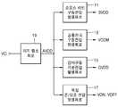
도 1은 LCD Driver IC에서 액정 구동과 관련된 회로들의 개략적인 블록도를 나타내는 도면이다.1 is a schematic block diagram of circuits related to driving a liquid crystal in an LCD driver IC.
도 2는 도 1의 LCD Driver IC의 파우워 온(power on) 동작 순서(sequence)를 타나내는 도면이다.FIG. 2 is a diagram illustrating a power on operation sequence of the LCD driver IC of FIG. 1.
도 3은 본 발명의 제1실시예에 따른 차지펌프 회로를 나타내는 도면이다.3 is a view showing a charge pump circuit according to a first embodiment of the present invention.
도 4는 본 발명의 제2실시예에 따른 차지펌프 회로를 나타내는 도면이다.4 is a view showing a charge pump circuit according to a second embodiment of the present invention.
본 발명은 LDI(LCD Driver IC)에 관한 것으로, 특히 LDI의 차지펌프(charge pump) 회로에 관한 것이다.BACKGROUND OF THE
모바일(Mobile) 기기용 LDI는 액정을 구동하기 위하여 도 1에 도시된 바와 같이 소오스 라인(Source line) 구동전압(SVDD)을 발생하는 회로(11), 공통 전극 구동전압(VCOM)을 발생하는 회로(13), 감마(Gamma) 구동 기준전압(GVDD)을 발생하는 회로(15), 및 액정 온/오프(on/off) 전압(VON,VOFF)을 발생하는 회로(17)를 포함한다. 소오스 라인 구동전압 발생 회로(11), 공통 전극 구동전압 발생 회로(13), 및 감마 구동 기준전압 발생 회로(15)는 증폭기들을 포함하여 구성된다.The LDI for a mobile device includes a
또한 LDI는 상기 회로들의 전원전압을 공급하기 위해 차지펌프 회로(19)를 포함한다. 차지펌프 회로(19)는 약 2.5볼트 내지 3.3볼트의 외부 배터리 전원전압(VCI)을 받아 이를 승압하여 약 5.5볼트의 승압전압(AVDD)을 발생하고 이 승압전압(AVDD)을 상기 회로들의 전원전압으로서 상기 회로들에 제공한다.The LDI also includes a
한편 도 1의 LDI는 각 회로에 안정적으로 전원전압을 공급하기 위해 도 2에 도시된 바와 같은 순서(sequence)에 의해 파우워 온(power on) 동작을 수행한다. 리셋 후 먼저 차지펌프 회로(19)가 온되어 승압전압(AVDD)이 발생되고 액정 온/오프 전압 발생회로(17)에 의해 액정 온/오프 전압(VON,VOFF)이 발생된다(S1 단계 및 S2 단계).Meanwhile, the LDI of FIG. 1 performs a power on operation by a sequence as shown in FIG. 2 in order to stably supply a power supply voltage to each circuit. After the reset, the
다음에 공통 전극 구동전압 발생 회로(13) 및 감마 구동 기준전압 발생회로(15)가 승압전압(AVDD)을 전원전압으로 사용하여 온되어 공통 전극 구동전압(VCOM) 및 감마 구동 기준전압(GVDD)이 발생된다(S3 단계 및 S4 단계).Next, the common electrode driving
마지막으로 LCD 패널을 구동하는 디스플레이 온 모드(Display on mode)로 진입하여 소오스 라인 구동전압 발생 회로(11)가 온된다(S5-S7 단계). 이때 디스플레이 온 모드(Display on mode)는 흑백 모드에 해당하는 바이너리 모드(Binary mode) 와 칼러 모드에 해당하는 그래디언트 모드(Gradient mode)로 이루어진다.Finally, the display panel enters a display on mode for driving the LCD panel, and the source line driving
바이너리 모드(Binary mode)에서는 소오스 라인 구동전압 발생 회로(11) 내의 증폭기들이 모두 오프되며 그래디언트 모드(Gradient mode)에서는 소오스 라인 구동전압 발생 회로(11) 내의 증폭기들이 모두 온된다. 따라서 그래디언트 모드시 가장 많은 수의 증폭기들이 동작하며 그 결과 그래디언트 모드시 차지펌프 회로(19)의 출력단의 부하가 가장 커지게 된다. 다시말해 그래디언트 모드시 승압전압(AVDD)에 의해 구동되는 부하의 크기가 가장 커지게 된다.In the binary mode, the amplifiers in the source line driving
한편 LDI에 채용되는 종래의 차지펌프 회로에서는 내부에서 발생된 승압전압을 차지펌프 회로의 출력단으로 전달하는 드라이버, 즉 구동 전달(transfer) 트랜지스터의 전류 구동능력이 상기 출력단의 부하가 가장 큰 상태인 디스플레이 온 모드의 그래디언트 모드를 기준으로 하여 고정된다.On the other hand, in the conventional charge pump circuit employed in the LDI, a display in which a driver for transferring a boost voltage generated internally to the output stage of the charge pump circuit, that is, a current transfer capability of a drive transfer transistor has the greatest load on the output stage It is fixed based on the gradient mode of the on mode.
이로 인하여 차지펌프 회로의 출력단의 부하가 작은 상태, 즉 그래디언트 모드 이외의 동작상태에서는 드라이버를 통해 과도하게 불필요한 전류소모가 발생되는 단점이 있다.As a result, excessively unnecessary current consumption is generated through the driver in a state in which the load of the output stage of the charge pump circuit is small, that is, in an operation state other than the gradient mode.
따라서 본 발명이 이루고자하는 기술적 과제는, 출력단의 부하가 변하더라도 불필요한 전류소모를 감소시킬 수 LDI의 차지펌프 회로를 제공하는 데 있다.Accordingly, an object of the present invention is to provide an LDI charge pump circuit that can reduce unnecessary current consumption even when the output stage load is changed.
상기 기술적 과제를 달성하기 위한 본 발명의 일면에 따른 차지펌프 회로는, 외부 전원전압을 받아 이를 승압하여 승압전압을 발생하는 차지펌프 부, 및 상기 승압전압을 출력단으로 전달하는 드라이버를 구비하고, 상기 드라이버의 전류 구동능력이 상기 승압전압에 의해 구동되는 부하의 크기에 따라 가변되는 것을 특징으로 한다.According to an aspect of the present invention, there is provided a charge pump circuit including a charge pump unit configured to receive an external power supply voltage and boost it to generate a boosted voltage, and a driver to transfer the boosted voltage to an output terminal. The current driving capability of the driver is variable according to the size of the load driven by the boost voltage.
바람직한 실시예에 따르면 상기 드라이버는 상기 차지펌프 부와 상기 출력단 사이에 병렬로 연결되는 적어도 두개 이상의 구동전달 트랜지스터들을 구비하고, 상기 부하의 크기에 따라 턴온되는 구동전달 트랜지스터들의 수가 가변된다.According to a preferred embodiment, the driver includes at least two drive transfer transistors connected in parallel between the charge pump unit and the output terminal, and the number of drive transfer transistors turned on according to the size of the load is variable.
상기 기술적 과제를 달성하기 위한 본 발명의 다른 일면에 따른 차지펌프 회로는, 소오스 라인 구동 증폭기들을 포함하며 제1동작 모드시에는 상기 소오스 라인 구동 증폭기들이 모두 온되고 제2동작 모드시에는 상기 소오스 라인 구동 증폭기들이 모두 오프되는 소오스 라인 구동전압 발생회로를 구비하는 LCD 드라이버의 차지펌프 회로에 있어서, 외부 전원전압을 받아 이를 승압하여 승압전압을 발생하는 차지펌프 부, 및 상기 승압전압을 상기 소오스 라인 구동전압 발생회로로 전달하는 드라이버를 구비하고, 상기 드라이버의 전류 구동능력이 상기 제1동작 모드 및 상기 제2동작 모드에 따라 가변되는 것을 특징으로 한다.According to another aspect of the present invention, a charge pump circuit includes source line driving amplifiers, and the source line driving amplifiers are all turned on in a first operation mode and the source line in a second operation mode. A charge pump circuit of an LCD driver including a source line driving voltage generation circuit in which driving amplifiers are all turned off, the charge pump circuit receiving a voltage from an external power supply and boosting the boosted voltage to generate a boosted voltage, and driving the boosted voltage to the source line. And a driver for transmitting to the voltage generating circuit, wherein the current driving capability of the driver is varied according to the first operation mode and the second operation mode.
바람직한 실시예에 따르면 상기 드라이버는, 제1제어신호의 활성화에 응답하여 상기 승압전압을 상기 소오스 라인 구동전압 발생회로로 전달하는 제1구동전달 트랜지스터, 및 상기 제1구동전달 트랜지스터와 병렬로 연결되고, 제2제어신호의 활성화에 응답하여 상기 승압전압을 상기 소오스 라인 구동전압 발생회로로 전달하는 제2구동전달 트랜지스터를 구비한다. 상기 제1동작 모드시에는 상기 제1제어신호 및 상기 제2제어신호가 모두 활성화되고 상기 제2동작 모드시에는 상기 제1제어 신호는 활성화되고 상기 제2제어신호는 비활성화된다.According to a preferred embodiment, the driver is connected in parallel with the first drive transfer transistor for transmitting the boosted voltage to the source line drive voltage generation circuit in response to the activation of a first control signal, and the first drive transfer transistor And a second driving transfer transistor configured to transfer the boosted voltage to the source line driving voltage generation circuit in response to activation of a second control signal. In the first operation mode, both the first control signal and the second control signal are activated. In the second operation mode, the first control signal is activated and the second control signal is deactivated.
상기 제1동작 모드는 상기 LCD 드라이버의 디스플레이 온 모드(Display on mode)의 그래디언트 모드(Gradient mode)이고 상기 제2동작 모드는 상기 LCD 드라이버의 디스플레이 온 모드(Display on mode)의 바이너리 모드(Binary mode)이다.The first operation mode is a gradient mode of the display on mode of the LCD driver and the second operation mode is a binary mode of the display on mode of the LCD driver. )to be.
본 발명과 본 발명의 동작 상의 잇점 및 본 발명의 실시에 의하여 달성되는 목적을 충분히 이해하기 위해서는 본 발명의 바람직한 실시예를 예시하는 첨부 도면 및 첨부 도면에 기재된 내용을 참조하여야만 한다.In order to fully understand the present invention, the operational advantages of the present invention, and the objects achieved by the practice of the present invention, reference should be made to the accompanying drawings illustrating preferred embodiments of the present invention and the contents described in the accompanying drawings.
이하, 첨부한 도면을 참조하여 본 발명의 바람직한 실시예를 설명함으로써, 본 발명을 상세히 설명한다. 각 도면에 제시된 동일한 참조부호는 동일한 부재를 나타낸다.Hereinafter, exemplary embodiments of the present invention will be described in detail with reference to the accompanying drawings. Like reference numerals in the drawings denote like elements.
도 3은 본 발명의 제1실시예에 따른 차지펌프 회로(39)를 나타내는 도면이다. 여기에서는 설명의 편의를 위하여 LCD Driver IC에서 액정 구동과 관련된 회로들(31,33,35,37)도 함께 도시되었다.3 is a view showing the
도 3을 참조하면, 본 발명의 제1실시예에 따른 차지펌프 회로(39)는 외부 전원전압(VCI)을 받아 이를 승압하여 승압전압을 발생하는 차지펌프 부(391) 및 상기 승압전압을 출력단으로 전달하는 드라이버(393)를 구비한다. 특히 드라이버(393)의 전류 구동능력은 차지펌프 회로(39)의 출력단의 부하의 크기에 따라 다시말해 차지펌프 회로(39)의 출력단으로부터 출력되는 승압전압(AVDD)에 의해 구동되는 부하의 크기에 따라 가변된다.Referring to FIG. 3, the
좀더 상세하게는, 드라이버(393)는 제1제어신호(VX)에 의해 제어되는 제1구 동전달 트랜지스터(P1) 및 제1구동전달 트랜지스터(P1)와 병렬로 연결되고 제2제어신호(VX_BINARY)에 의해 제어되는 제2구동전달 트랜지스터(P2)로 구성된다.More specifically, the
LCD 드라이버의 제1동작 모드, 즉 소오스 라인 구동전압 발생 회로(31) 내의 증폭기들이 모두 온되어 차지펌프 회로(39)의 출력단의 부하가 가장 커지는 디스플레이 온 모드(Display on mode)의 그래디언트 모드(Gradient mode)에서는, 제1제어신호(VX) 및 제2제어신호(VX_BINARY)가 모두 활성화된다. LCD 드라이버의 제2동작 모드, 즉 소오스 라인 구동전압 발생 회로(31) 내의 증폭기들이 모두 오프되어 차지펌프 회로(39)의 출력단의 부하가 작아지는 디스플레이 온 모드(Display on mode)의 바이너리 모드(Binary mode)에서는, 제1제어신호(VX)는 활성화되고 제2제어신호(VX_BINARY)는 비활성화된다.Gradient mode of the display on mode in which the first operation mode of the LCD driver, that is, the amplifiers in the source line driving
따라서 차지펌프 회로(39)의 출력단의 부하가 가장 커지는 그래디언트 모드(Gradient mode)에서는 제1구동전달 트랜지스터(P1) 및 제2구동전달 트랜지스터(P2)가 모두 턴온되어 드라이버(393)의 전류 구동능력이 커진다. 반면에 차지펌프 회로(39)의 출력단의 부하가 작아지는 바이너리 모드(Binary mode)에서는 제1구동전달 트랜지스터(P1)는 턴온되고 제2구동전달 트랜지스터(P2)는 턴오프되어 드라이버(393)의 전류 구동능력이 작아진다.Therefore, in the gradient mode in which the load of the output terminal of the
한편 차지펌프 부(391)는, 일단이 외부 전원전압(VCI)에 연결되는 제1스위치(S1), 일단이 제1스위치(S1)의 타단에 연결되는 커패시터(C1), 일단이 접지전압(GND)에 연결되고 타단이 커패시터(C1)의 타단에 연결되는 제2스위치(S2), 및 일단이 외부 전원전압(VCI)에 연결되고 타단이 커패시터(C1)의 타단에 연결되는 제3스위치(S3)를 구비한다. 제1스위치(S1)와 커패시터(C1) 간의 접속노드(N1)로부터 승압전압이 출력된다. 제1 내지 제3스위치(S1-S3)는 모스 트랜지스터로 구성되는 것이 바람직하다. 차지펌프 부(391)는 다른 여러가지 다양한 형태로 구성될 수 있음은 자명하다.Meanwhile, the
차지펌프 부(391)의 동작을 간단히 설명하면, 초기에 제1스위치(S1)가 온되어 제1스위치(S1)와 커패시터(C1) 간의 접속노드(N1)의 레벨이 외부 전원전압(VCI) 레벨이 된다. 다음에 제1스위치(S1)가 오프되고 제2스위치(S2)가 온되면, 접속노드(N1)의 레벨은 외부 전원전압(VCI) 레벨을 유지하고 노드(N2)의 레벨은 접지전압(GND) 레렐이 된다. 다음에 제2스위치(S2)가 오프되고 제3스위치(S3)가 온되면, 노드(N2)의 레벨은 외부 전원전압(VCI) 레벨이 되고 이에 따라 접속노드(N1)의 레벨은 외부 전원전압(VCI) 레벨의 2배로 승압된다.Briefly describing the operation of the
한편 차지펌프 회로(39)의 출력단으로부터 출력되는 승압전압(AVDD)은 LCD Driver IC에서 액정 구동과 관련된 여러 회로들(31,33,35,37)에 전원전압으로서 제공된다. 소오스 라인 구동전압 발생 회로(31)는 소오스 라인 구동전압(SVDD)을 발생한다. 공통 전극 구동전압 발생 회로(33)는 공통 전극 구동전압(VCOM)을 발생한다. 감마(Gamma) 구동 기준전압 발생 회로(35)는 감마 구동 기준전압(GVDD)을 발생한다. 액정 온/오프 전압 발생 회로(37)는 액정을 온/오프(on/off)시키기 위한 전압(VON,VOFF)을 발생한다. 이러한 회로들은 LCD Driver IC에 포함되는 통상적인 것들이므로 여기에서 상세한 구성에 대해서는 생략된다.On the other hand, the boost voltage AVDD output from the output terminal of the
이상에서와 같이 본 발명의 제1실시예에 따른 차지펌프 회로에서는 차지펌프 회로의 출력단의 부하가 가장 커지는 그래디언트 모드(Gradient mode)에서는 내부의 드라이버(393)의 전류 구동능력이 커지고 차지펌프 회로의 출력단의 부하가 작아지는 바이너리 모드(Binary mode)에서는 내부의 드라이버(393)의 전류 구동능력이 작아진다.As described above, in the charge pump circuit according to the first embodiment of the present invention, in the gradient mode in which the load of the output terminal of the charge pump circuit is the greatest, the current driving capability of the
다시말해 차지펌프 회로의 출력단의 부하가 작아지는 바이너리 모드에서는 드라이버(393)의 전류 구동능력이 작아도 되므로 제2구동전달 트랜지스터(P2)는 턴오프되고 제1구동전달 트랜지스터(P1)만 동작된다. 이에 따라 과도하게 큰 구동 트랜지스터의 크기로 인해 발생되는 불필요한 전류소모가 방지될 수 있으며 또한 승압효율이 적정수준으로 유지되어 공정내압을 넘는 동작이 방지될 수 있다.In other words, in the binary mode in which the load of the output terminal of the charge pump circuit is small, the current driving capability of the
도 4는 본 발명의 제2실시예에 따른 차지펌프 회로(39A)를 나타내는 도면이다.4 is a view showing the
도 4를 참조하면, 본 발명의 제2실시예에 따른 차지펌프 회로(39A)는 드라이버(393A)의 구성이 제1실시예와 다르다. 드라이버(393A)의 전류 구동능력은 차지펌프 회로(39A)의 출력단의 부하의 크기에 따라 다시말해 차지펌프 회로(39A)의 출력단으로부터 출력되는 승압전압(AVDD)에 의해 구동되는 부하의 크기에 따라 가변된다.4, the configuration of the
좀더 상세하게는, 드라이버(393A)는 각각의 제어신호(VA,VB,VC,VD,VN)에 의해 제어되고 서로 병렬로 연결되는 복수개의 구동전달 트랜지스터들(P3-P7)을 구비한다. 그리고 차지펌프 회로(39A)의 출력단의 부하의 크기에 따라 제어신호(VA,VB,VC,VD,VN)에 의해 구동전달 트랜지스터들(P3-P7)중 턴온되는 것들 의 수가 가변된다.More specifically, the
다시말해 그래디언트 모드 및 바이너리 모드 뿐만 아니라 차지펌프 회로(39A)의 출력단의 부하의 크기가 변경되는 LCD 드라이버의 다른 여러가지 동작모드에서도 구동전달 트랜지스터들(P3-P7)을 선택적으로 동작시킴으로써 드라이버(393A)에서의 불필요한 전류소모가 방지될 수 있으며 또한 승압효율이 적정수준으로 유지될 수 있다.In other words, the
이상 도면과 명세서에서 최적 실시예가 개시되었다. 여기서 특정한 용어들이 사용되었으나, 이는 단지 본 발명을 설명하기 위한 목적에서 사용된 것이지 의미한정이나 특허청구범위에 기재된 본 발명의 범위를 제한하기 위하여 사용된 것은 아니다. 그러므로 본 기술 분야의 통상의 지식을 가진 자라면 이로부터 다양한 변형 및 균등한 타 실시예가 가능하다는 점을 이해할 것이다. 따라서, 본 발명의 진정한 기술적 보호 범위는 첨부된 특허청구범위의 기술적 사상에 의해 정해져야 할 것이다.The best embodiment has been disclosed in the drawings and specification above. Although specific terms have been used herein, they are used only for the purpose of describing the present invention and are not intended to limit the scope of the invention as defined in the claims or the claims. Therefore, those skilled in the art will understand that various modifications and equivalent other embodiments are possible from this. Therefore, the true technical protection scope of the present invention will be defined by the technical spirit of the appended claims.
상술한 바와 같이 본 발명에 따른 LCD 드라이버의 차지펌프 회로는 동작모드에 따라 출력단의 부하가 변하더라도 불필요한 전류소모가 발생되는 것을 방지할 수 있으며 또한 승압효율을 적정수준으로 유지할 수 있는 장점이 있다.As described above, the charge pump circuit of the LCD driver according to the present invention can prevent unnecessary current consumption even when the load of the output stage is changed according to the operation mode, and has an advantage of maintaining the boosting efficiency at an appropriate level.
Claims (10)
Translated fromKoreanPriority Applications (2)
| Application Number | Priority Date | Filing Date | Title |
|---|---|---|---|
| KR1020040031354AKR100604849B1 (en) | 2004-05-04 | 2004-05-04 | Charge pump circuit of LC driver including driver whose current driving capability is changed according to the size of load of output stage |
| US11/121,540US7230471B2 (en) | 2004-05-04 | 2005-05-04 | Charge pump circuit of LCD driver including driver having variable current driving capability |
Applications Claiming Priority (1)
| Application Number | Priority Date | Filing Date | Title |
|---|---|---|---|
| KR1020040031354AKR100604849B1 (en) | 2004-05-04 | 2004-05-04 | Charge pump circuit of LC driver including driver whose current driving capability is changed according to the size of load of output stage |
Publications (2)
| Publication Number | Publication Date |
|---|---|
| KR20050106578A KR20050106578A (en) | 2005-11-10 |
| KR100604849B1true KR100604849B1 (en) | 2006-07-26 |
Family
ID=35238924
Family Applications (1)
| Application Number | Title | Priority Date | Filing Date |
|---|---|---|---|
| KR1020040031354AExpired - Fee RelatedKR100604849B1 (en) | 2004-05-04 | 2004-05-04 | Charge pump circuit of LC driver including driver whose current driving capability is changed according to the size of load of output stage |
Country Status (2)
| Country | Link |
|---|---|
| US (1) | US7230471B2 (en) |
| KR (1) | KR100604849B1 (en) |
Families Citing this family (8)
| Publication number | Priority date | Publication date | Assignee | Title |
|---|---|---|---|---|
| US7751643B2 (en)* | 2004-08-12 | 2010-07-06 | Semiconductor Insights Inc. | Method and apparatus for removing uneven brightness in an image |
| US20090066407A1 (en)* | 2007-09-12 | 2009-03-12 | Rochester Institute Of Technology | Charge pump systems and methods thereof |
| KR20090080258A (en) | 2008-01-21 | 2009-07-24 | 삼성전자주식회사 | Display device including a boosting voltage generator and the boosting voltage generator to increase the boosting efficiency according to the load amount |
| KR101102969B1 (en)* | 2010-02-25 | 2012-01-10 | 매그나칩 반도체 유한회사 | Semiconductor devices |
| KR102414300B1 (en) | 2015-08-26 | 2022-06-30 | 삼성전자주식회사 | Operating Module for display and operating Method, and electronic device supporting the same |
| CN110024280B (en)* | 2016-11-03 | 2023-12-15 | 思睿逻辑国际半导体有限公司 | Variable ratio charge pump with peak and average current limiting circuits |
| JP2023004758A (en)* | 2021-06-28 | 2023-01-17 | 株式会社ジャパンディスプレイ | Display panel and electronic apparatus |
| CN113630114B (en)* | 2021-08-18 | 2024-11-05 | 上海数明半导体有限公司 | Driving circuit and electronic equipment |
Family Cites Families (13)
| Publication number | Priority date | Publication date | Assignee | Title |
|---|---|---|---|---|
| US4897774A (en)* | 1985-10-01 | 1990-01-30 | Maxim Integrated Products | Integrated dual charge pump power supply and RS-232 transmitter/receiver |
| US4812961A (en)* | 1987-05-15 | 1989-03-14 | Linear Technology, Inc. | Charge pump circuitry having low saturation voltage and current-limited switch |
| US5130571A (en)* | 1990-08-29 | 1992-07-14 | Ventritex | Optimizing speed and charge injection parameters of a switched capacitor circuit |
| JP3292417B2 (en)* | 1994-02-15 | 2002-06-17 | 三菱電機株式会社 | Semiconductor device |
| US5550728A (en)* | 1994-04-18 | 1996-08-27 | Analog Devices, Inc. | Charge pump converter structure |
| US5912560A (en)* | 1997-02-25 | 1999-06-15 | Waferscale Integration Inc. | Charge pump circuit for voltage boosting in integrated semiconductor circuits |
| KR100295053B1 (en)* | 1998-09-03 | 2001-07-12 | 윤종용 | Load adaptive low noise output buffer |
| JP3487581B2 (en) | 1998-09-22 | 2004-01-19 | シャープ株式会社 | Power supply circuit and display device and electronic equipment using the same |
| JP4212791B2 (en) | 2000-08-09 | 2009-01-21 | シャープ株式会社 | Liquid crystal display device and portable electronic device |
| US6411531B1 (en)* | 2000-11-21 | 2002-06-25 | Linear Technology Corporation | Charge pump DC/DC converters with reduced input noise |
| US6466079B1 (en)* | 2001-06-21 | 2002-10-15 | Tower Semiconductor Ltd. | High voltage charge pump for providing output voltage close to maximum high voltage of a CMOS device |
| KR20010113589A (en) | 2001-09-25 | 2001-12-28 | 이경수 | Leaflet Lottery |
| US6937487B1 (en)* | 2003-04-29 | 2005-08-30 | National Semiconductor Corporation | Apparatus and method for a voltage booster with improved voltage regulator efficiency |
- 2004
- 2004-05-04KRKR1020040031354Apatent/KR100604849B1/ennot_activeExpired - Fee Related
- 2005
- 2005-05-04USUS11/121,540patent/US7230471B2/ennot_activeExpired - Fee Related
Also Published As
| Publication number | Publication date |
|---|---|
| US20050248388A1 (en) | 2005-11-10 |
| US7230471B2 (en) | 2007-06-12 |
| KR20050106578A (en) | 2005-11-10 |
Similar Documents
| Publication | Publication Date | Title |
|---|---|---|
| KR101579838B1 (en) | Apparatus using a stabilized driving voltage and display system using the same | |
| US20080084371A1 (en) | Liquid crystal display for preventing residual image phenomenon and related method thereof | |
| JP2004226787A (en) | Display device | |
| KR100741471B1 (en) | Boosting scheme without latch-up | |
| US8754838B2 (en) | Discharge circuit and display device with the same | |
| US7436385B2 (en) | Analog buffer and driving method thereof, liquid crystal display apparatus using the same and driving method thereof | |
| JP2001286126A (en) | Charge pump power source circuit, display drive device using it and display | |
| US20070241952A1 (en) | Digital to analog converter having integrated level shifter and method for using same to drive display device | |
| KR100604849B1 (en) | Charge pump circuit of LC driver including driver whose current driving capability is changed according to the size of load of output stage | |
| JP4462844B2 (en) | Power circuit | |
| JP2006201760A (en) | Display device drive circuit and drive method | |
| US7605641B2 (en) | Apparatus comprising a charge pump and LCD driver comprising such an apparatus | |
| US20130113776A1 (en) | Power Management Circuit and Gate Pulse Modulation Circuit Thereof | |
| US20180061342A1 (en) | Semiconductor device, power supply circuit, and liquid crystal display device | |
| CN110718199A (en) | Display panel and its booster circuit | |
| JP2000056741A (en) | Liquid crystal panel drive circuit and liquid crystal display device | |
| US8599184B2 (en) | Charge pump and display driving system including the same | |
| US10135444B2 (en) | Semiconductor device with booster part, and booster | |
| JP4498073B2 (en) | Charge pump circuit | |
| KR20100125077A (en) | Boosting voltage generating circuit and display device comprising the same | |
| JP2008107855A (en) | Display apparatus | |
| KR101217158B1 (en) | Liquid crystal display device | |
| US20050110764A1 (en) | Battery operated device with display | |
| KR100602984B1 (en) | Power supply circuit | |
| US20090167744A1 (en) | Electro-optical device and electronic apparatus provided with the same |
Legal Events
| Date | Code | Title | Description |
|---|---|---|---|
| A201 | Request for examination | ||
| PA0109 | Patent application | St.27 status event code:A-0-1-A10-A12-nap-PA0109 | |
| PA0201 | Request for examination | St.27 status event code:A-1-2-D10-D11-exm-PA0201 | |
| R17-X000 | Change to representative recorded | St.27 status event code:A-3-3-R10-R17-oth-X000 | |
| PN2301 | Change of applicant | St.27 status event code:A-3-3-R10-R13-asn-PN2301 St.27 status event code:A-3-3-R10-R11-asn-PN2301 | |
| PN2301 | Change of applicant | St.27 status event code:A-3-3-R10-R13-asn-PN2301 St.27 status event code:A-3-3-R10-R11-asn-PN2301 | |
| D13-X000 | Search requested | St.27 status event code:A-1-2-D10-D13-srh-X000 | |
| D14-X000 | Search report completed | St.27 status event code:A-1-2-D10-D14-srh-X000 | |
| E902 | Notification of reason for refusal | ||
| PE0902 | Notice of grounds for rejection | St.27 status event code:A-1-2-D10-D21-exm-PE0902 | |
| PG1501 | Laying open of application | St.27 status event code:A-1-1-Q10-Q12-nap-PG1501 | |
| T11-X000 | Administrative time limit extension requested | St.27 status event code:U-3-3-T10-T11-oth-X000 | |
| T11-X000 | Administrative time limit extension requested | St.27 status event code:U-3-3-T10-T11-oth-X000 | |
| P11-X000 | Amendment of application requested | St.27 status event code:A-2-2-P10-P11-nap-X000 | |
| P13-X000 | Application amended | St.27 status event code:A-2-2-P10-P13-nap-X000 | |
| E701 | Decision to grant or registration of patent right | ||
| PE0701 | Decision of registration | St.27 status event code:A-1-2-D10-D22-exm-PE0701 | |
| GRNT | Written decision to grant | ||
| PR0701 | Registration of establishment | St.27 status event code:A-2-4-F10-F11-exm-PR0701 | |
| PR1002 | Payment of registration fee | St.27 status event code:A-2-2-U10-U11-oth-PR1002 Fee payment year number:1 | |
| PG1601 | Publication of registration | St.27 status event code:A-4-4-Q10-Q13-nap-PG1601 | |
| PR1001 | Payment of annual fee | St.27 status event code:A-4-4-U10-U11-oth-PR1001 Fee payment year number:4 | |
| PR1001 | Payment of annual fee | St.27 status event code:A-4-4-U10-U11-oth-PR1001 Fee payment year number:5 | |
| PR1001 | Payment of annual fee | St.27 status event code:A-4-4-U10-U11-oth-PR1001 Fee payment year number:6 | |
| R18-X000 | Changes to party contact information recorded | St.27 status event code:A-5-5-R10-R18-oth-X000 | |
| PR1001 | Payment of annual fee | St.27 status event code:A-4-4-U10-U11-oth-PR1001 Fee payment year number:7 | |
| FPAY | Annual fee payment | Payment date:20130701 Year of fee payment:8 | |
| PR1001 | Payment of annual fee | St.27 status event code:A-4-4-U10-U11-oth-PR1001 Fee payment year number:8 | |
| FPAY | Annual fee payment | Payment date:20140630 Year of fee payment:9 | |
| PR1001 | Payment of annual fee | St.27 status event code:A-4-4-U10-U11-oth-PR1001 Fee payment year number:9 | |
| LAPS | Lapse due to unpaid annual fee | ||
| PC1903 | Unpaid annual fee | St.27 status event code:A-4-4-U10-U13-oth-PC1903 Not in force date:20150720 Payment event data comment text:Termination Category : DEFAULT_OF_REGISTRATION_FEE | |
| PC1903 | Unpaid annual fee | St.27 status event code:N-4-6-H10-H13-oth-PC1903 Ip right cessation event data comment text:Termination Category : DEFAULT_OF_REGISTRATION_FEE Not in force date:20150720 |