KR100604751B1 - Acid Resistant Photoresist Copolymer and Photoresist Composition Containing the Same - Google Patents
Acid Resistant Photoresist Copolymer and Photoresist Composition Containing the SameDownload PDFInfo
- Publication number
- KR100604751B1 KR100604751B1KR1020010051442AKR20010051442AKR100604751B1KR 100604751 B1KR100604751 B1KR 100604751B1KR 1020010051442 AKR1020010051442 AKR 1020010051442AKR 20010051442 AKR20010051442 AKR 20010051442AKR 100604751 B1KR100604751 B1KR 100604751B1
- Authority
- KR
- South Korea
- Prior art keywords
- formula
- mol
- photoresist
- compound
- copolymer
- Prior art date
- Legal status (The legal status is an assumption and is not a legal conclusion. Google has not performed a legal analysis and makes no representation as to the accuracy of the status listed.)
- Expired - Fee Related
Links
- 0CCC1C(*C(C2*(*C(C(**C(C(*C)C(O3)=O)C3=O)C(C3)C4)C3C4C(OC(C)(C)C)=O)C2C(C2)C3)C2C3C(OCCO)=O)COCCOCCOC1Chemical compoundCCC1C(*C(C2*(*C(C(**C(C(*C)C(O3)=O)C3=O)C(C3)C4)C3C4C(OC(C)(C)C)=O)C2C(C2)C3)C2C3C(OCCO)=O)COCCOCCOC10.000description2
- OFDVXLAEUUTSDI-UHFFFAOYSA-NC1C2C=CC1C1C2COCCOCCOC1Chemical compoundC1C2C=CC1C1C2COCCOCCOC1OFDVXLAEUUTSDI-UHFFFAOYSA-N0.000description1
- TVCYUBRCMLMVBL-UHFFFAOYSA-NC1C2C=CC1CC21COCCOCCOC1Chemical compoundC1C2C=CC1CC21COCCOCCOC1TVCYUBRCMLMVBL-UHFFFAOYSA-N0.000description1
Images


Classifications
- G—PHYSICS
- G03—PHOTOGRAPHY; CINEMATOGRAPHY; ANALOGOUS TECHNIQUES USING WAVES OTHER THAN OPTICAL WAVES; ELECTROGRAPHY; HOLOGRAPHY
- G03F—PHOTOMECHANICAL PRODUCTION OF TEXTURED OR PATTERNED SURFACES, e.g. FOR PRINTING, FOR PROCESSING OF SEMICONDUCTOR DEVICES; MATERIALS THEREFOR; ORIGINALS THEREFOR; APPARATUS SPECIALLY ADAPTED THEREFOR
- G03F7/00—Photomechanical, e.g. photolithographic, production of textured or patterned surfaces, e.g. printing surfaces; Materials therefor, e.g. comprising photoresists; Apparatus specially adapted therefor
- G03F7/004—Photosensitive materials
- G03F7/027—Non-macromolecular photopolymerisable compounds having carbon-to-carbon double bonds, e.g. ethylenic compounds
- C—CHEMISTRY; METALLURGY
- C07—ORGANIC CHEMISTRY
- C07D—HETEROCYCLIC COMPOUNDS
- C07D273/00—Heterocyclic compounds containing rings having nitrogen and oxygen atoms as the only ring hetero atoms, not provided for by groups C07D261/00 - C07D271/00
- C—CHEMISTRY; METALLURGY
- C07—ORGANIC CHEMISTRY
- C07D—HETEROCYCLIC COMPOUNDS
- C07D323/00—Heterocyclic compounds containing more than two oxygen atoms as the only ring hetero atoms
- G—PHYSICS
- G03—PHOTOGRAPHY; CINEMATOGRAPHY; ANALOGOUS TECHNIQUES USING WAVES OTHER THAN OPTICAL WAVES; ELECTROGRAPHY; HOLOGRAPHY
- G03F—PHOTOMECHANICAL PRODUCTION OF TEXTURED OR PATTERNED SURFACES, e.g. FOR PRINTING, FOR PROCESSING OF SEMICONDUCTOR DEVICES; MATERIALS THEREFOR; ORIGINALS THEREFOR; APPARATUS SPECIALLY ADAPTED THEREFOR
- G03F7/00—Photomechanical, e.g. photolithographic, production of textured or patterned surfaces, e.g. printing surfaces; Materials therefor, e.g. comprising photoresists; Apparatus specially adapted therefor
- G03F7/004—Photosensitive materials
- G03F7/039—Macromolecular compounds which are photodegradable, e.g. positive electron resists
- G03F7/0392—Macromolecular compounds which are photodegradable, e.g. positive electron resists the macromolecular compound being present in a chemically amplified positive photoresist composition
- G03F7/0395—Macromolecular compounds which are photodegradable, e.g. positive electron resists the macromolecular compound being present in a chemically amplified positive photoresist composition the macromolecular compound having a backbone with alicyclic moieties
- G—PHYSICS
- G03—PHOTOGRAPHY; CINEMATOGRAPHY; ANALOGOUS TECHNIQUES USING WAVES OTHER THAN OPTICAL WAVES; ELECTROGRAPHY; HOLOGRAPHY
- G03F—PHOTOMECHANICAL PRODUCTION OF TEXTURED OR PATTERNED SURFACES, e.g. FOR PRINTING, FOR PROCESSING OF SEMICONDUCTOR DEVICES; MATERIALS THEREFOR; ORIGINALS THEREFOR; APPARATUS SPECIALLY ADAPTED THEREFOR
- G03F7/00—Photomechanical, e.g. photolithographic, production of textured or patterned surfaces, e.g. printing surfaces; Materials therefor, e.g. comprising photoresists; Apparatus specially adapted therefor
- G03F7/004—Photosensitive materials
- G03F7/039—Macromolecular compounds which are photodegradable, e.g. positive electron resists
- G03F7/0392—Macromolecular compounds which are photodegradable, e.g. positive electron resists the macromolecular compound being present in a chemically amplified positive photoresist composition
- G03F7/0397—Macromolecular compounds which are photodegradable, e.g. positive electron resists the macromolecular compound being present in a chemically amplified positive photoresist composition the macromolecular compound having an alicyclic moiety in a side chain
- Y—GENERAL TAGGING OF NEW TECHNOLOGICAL DEVELOPMENTS; GENERAL TAGGING OF CROSS-SECTIONAL TECHNOLOGIES SPANNING OVER SEVERAL SECTIONS OF THE IPC; TECHNICAL SUBJECTS COVERED BY FORMER USPC CROSS-REFERENCE ART COLLECTIONS [XRACs] AND DIGESTS
- Y10—TECHNICAL SUBJECTS COVERED BY FORMER USPC
- Y10S—TECHNICAL SUBJECTS COVERED BY FORMER USPC CROSS-REFERENCE ART COLLECTIONS [XRACs] AND DIGESTS
- Y10S430/00—Radiation imagery chemistry: process, composition, or product thereof
- Y10S430/143—Electron beam
Landscapes
- Physics & Mathematics (AREA)
- Spectroscopy & Molecular Physics (AREA)
- Chemical & Material Sciences (AREA)
- Organic Chemistry (AREA)
- General Physics & Mathematics (AREA)
- Materials For Photolithography (AREA)
- Addition Polymer Or Copolymer, Post-Treatments, Or Chemical Modifications (AREA)
- Exposure And Positioning Against Photoresist Photosensitive Materials (AREA)
Abstract
Translated fromKorean
Description
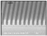
Translated fromKorean도 1은 본 발명의 실시예 14에서 얻어진 패턴의 사진이고,1 is a photograph of a pattern obtained in Example 14 of the present invention,
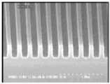
도 2는 본 발명의 실시예 15에서 얻어진 패턴의 사진이고,2 is a photograph of a pattern obtained in Example 15 of the present invention,
도 3은 본 발명의 실시예 16에서 얻어진 패턴의 사진이고,3 is a photograph of a pattern obtained in Example 16 of the present invention,
도 4는 본 발명의 실시예 17에서 얻어진 패턴의 사진이고,4 is a photograph of a pattern obtained in Example 17 of the present invention,
도 5는 본 발명의 실시예 18에서 얻어진 패턴의 사진이고,5 is a photograph of a pattern obtained in Example 18 of the present invention,
도 6은 본 발명의 실시예 19에서 얻어진 패턴의 사진이며,6 is a photograph of a pattern obtained in Example 19 of the present invention,
도 7은 본 발명의 실시예 20에서 얻어진 패턴의 사진이다.7 is a photograph of a pattern obtained in Example 20 of the present invention.
본 발명은 산 확산 방지용 포토레지스트 공중합체 및 이를 함유하는 포토레지스트 조성물에 관한 것으로서, 더욱 상세하게는 포토리소그래피 공정 중 노광 공정에 의해 노광부에서 발생된 산이 비노광부로 확산되는 것을 방지하기 위하여 사용하는 포토레지스트 공중합체, 그 공중합체를 함유하는 포토레지스트 조성물 및 이를 이용한 패턴 형성방법에 관한 것이다.The present invention relates to a photoresist copolymer for preventing acid diffusion and a photoresist composition containing the same, and more particularly, to prevent the acid generated in the exposed portion by the exposure process during the photolithography process from being diffused into the non-exposed portion. It relates to a photoresist copolymer, a photoresist composition containing the copolymer and a pattern forming method using the same.
반도체 제조공정에 있어 고감도의 초미세 패턴을 형성하기 위해, 근래에는 화학증폭성인 DUV(Deep Ultra Violet) 포토레지스트가 각광을 받고 있으며, 그 조성은 광산발생제(photoacid generator)와 산에 민감하게 반응하는 구조의 고분자 화합물을 배합하여 제조한다.In order to form a highly sensitive ultra-fine pattern in the semiconductor manufacturing process, a chemically amplified deep ultra violet (DUV) photoresist has recently been spotlighted, and its composition is sensitive to photoacid generators and acids. It manufactures by mix | blending the high molecular compound of the structure which is.
이러한 포토레지스트의 작용 기전은 광산발생제가 광원으로부터 자외선 빛을 받게 되면 산을 발생시키고, 이렇게 발생된 산에 의해 노광후 베이크 공정에서 매트릭스 고분자 화합물의 주쇄 또는 측쇄가 반응하여 분해되거나, 가교결합되면서 고분자 화합물의 극성이 크게 변하여, 노광부위와 비노광부위가 현상액에 대해 서로 다른 용해도를 갖게 된다. 예를 들어, 포지티브 포토레지스트의 경우, 노광부에서는 산이 발생되고, 발생된 산이 노광후 베이크 공정에서 매트릭스 고분자 화합물과 반응하여 고분자의 주쇄 또는 측쇄가 분해되어 후속 현상공정에서 녹아 없어지게 된다. 반면, 비노광부위에서는 산이 발생되지 않으므로 본래의 고분자 화합물 구조를 그대로 갖기 때문에 후속 현상공정에서 녹지 않는다. 그 결과, 마스크의 상이 기판 위에 양화상으로 남겨진다.The action mechanism of the photoresist generates acid when the photoacid generator receives ultraviolet light from a light source, and the acid generated in the photoresist reacts with the main chain or side chain of the matrix polymer compound in the post-exposure bake process to decompose or crosslink the polymer. The polarity of the compound changes greatly, so that the exposed portion and the non-exposed portion have different solubility in the developer. For example, in the case of a positive photoresist, an acid is generated in the exposed portion, and the generated acid reacts with the matrix polymer compound in the post-exposure bake process so that the main chain or side chain of the polymer is decomposed and melted in a subsequent developing process. On the other hand, since no acid is generated in the non-exposed part, since it has the original polymer compound structure, it does not melt in a subsequent developing process. As a result, the image of the mask is left as a positive image on the substrate.
그런데, 노광공정 또는 노광후 지연(PED ; post exposure delay)시에 노광부에서 발생된 산의 일부가 비노광부로 불규칙적으로 확산됨으로써 라인 가장자리 거칠음 (Line Edge Roughness : 이하 "LER"이라 칭함)이 심해지고 패턴의 모양이 일그러지는 현상, 즉 탑 로스 (Top loss)나 슬로우프 (slope)가 관찰되었다.However, a part of the acid generated in the exposure part is irregularly diffused into the non-exposure part during the exposure process or the post exposure delay (PED), so that the line edge roughness (hereinafter referred to as "LER") is severe. Loss and slope of the pattern was observed, ie Top Loss or Slope.
이러한 산 확산 현상을 방지하기 위해, 종래에는 노광공정에서 발생된 산과 결합가능한 약염기성 아민 또는 아미드 화합물을 화학증폭형 포토레지스트 조성물에 첨가함으로써, 노광부에서 발생된 산이 비노광부로 확산되는 것을 방지하고 있다.In order to prevent such acid diffusion, conventionally, by adding a weakly basic amine or amide compound which can be combined with an acid generated in the exposure process to the chemically amplified photoresist composition, the acid generated in the exposed portion is prevented from diffusing into the non-exposed portion. have.
그러나, 상기 아민 또는 아미드 화합물은 250nm 이하의 극단파장 영역, 예를 들어 ArF(193nm)의 파장영역에서 광흡수도가 커서 포토레지스트 조성물의 감도(sensitivity)를 저하시키는 문제가 있었다. 아울러 이들 염기의 확산 또한 불균일하기 때문에 LER이 커지는 효과를 초래하였다.However, the amine or amide compound has a problem of lowering the sensitivity of the photoresist composition due to its high light absorption in a wavelength region of 250 nm or less, for example, in the wavelength region of ArF (193 nm). In addition, the diffusion of these bases is also nonuniform, leading to an effect of increasing LER.
상기한 문제점을 해결하기 위하여, 본 발명에서는 극단파장 영역에서 광흡수도가 낮으면서도, 노광부에서 발생된 산의 확산을 효과적으로 방지할 수 있는 포토레지스트 공중합체 및 그 공중합체를 함유하는 포토레지스트 조성물을 제공하는 것을 목적으로 한다.In order to solve the above problems, in the present invention, a photoresist copolymer and a photoresist composition containing the copolymer can effectively prevent the diffusion of acid generated in the exposure portion while having low light absorption in the extreme wavelength region. The purpose is to provide.
또한, 상기 산 확산 방지용 포토레지스트 공중합체를 함유하는 포토레지스트 조성물을 사용함으로써, 250nm 이하의 극단파장 광원을 채용하는 리소그래피 공정에서 보다 우수한 프로파일을 갖는 미세패턴 형성방법을 제공하는 것을 목적으로 한다.In addition, an object of the present invention is to provide a method of forming a fine pattern having a better profile in a lithography process employing an ultra-short wavelength light source of 250 nm or less by using a photoresist composition containing the acid diffusion preventing photoresist copolymer.
상기 목적을 달성하기 위해 본 발명에서는 산 확산 방지용 포토레지스트 공중합체를 제공한다.In order to achieve the above object, the present invention provides a photoresist copolymer for preventing acid diffusion.
또한, 본 발명에서는 상기한 산 확산 방지용 포토레지스트 공중합체를 함유 하는 포토레지스트 조성물 및 이를 이용하여 포토레지스트 미세 패턴을 형성하는 방법을 제공한다.In addition, the present invention provides a photoresist composition containing the above-mentioned photoresist copolymer for acid diffusion prevention and a method of forming a photoresist fine pattern using the same.
본 발명자들은 많은 연구와 실험을 거쳐, 에틸렌옥시 구조 단위를 포함하는 다산소 함유 화합물이 노광공정에서 발생된 산의 확산을 방지하는데 효과적이라는 사실에 기인하여, 적어도 1 이상의 공중합 가능한 탄소-탄소 이중결합을 갖는 동시에 에틸렌옥시 구조 단위를 포함하는 다산소 함유 화합물의 반복단위를 포함하는 공중합체가 산 확산 방지용 포토레지스트 공중합체로 사용되기에 적합함을 발견하였다.The inventors have, through many studies and experiments, at least one copolymerizable carbon-carbon double bond due to the fact that polyoxygen-containing compounds comprising ethyleneoxy structural units are effective in preventing the diffusion of acids generated during the exposure process. It has been found that a copolymer comprising a repeating unit of a polyoxygen-containing compound having an ethyleneoxy structural unit and having an ethyleneoxy structural unit is suitable for use as a photoresist copolymer for preventing acid diffusion.
즉, 대부분의 산소를 함유하는 화합물 예를 들어, 에테르의 경우, 염기성 (basicity)이 무시할 수 있을 정도로 미약하다. 그러나, 수 개의 산소를 함유하는 크라운 에테르 화합물의 경우, 여러 개의 산소가 규칙적으로 배열되어 있으며, 이들의 고립전자쌍이 좁은 공간에 밀집되어 협동효과 (cooperative effect)를 나타내므로, 일반적인 에테르 화합물과 달리 상당한 정도의 염기성을 띄게 된다. 더구나, 에틸렌옥시 구조 단위를 포함하는 다산소 함유 화합물은 일반적으로 산 또는 양이온 수송능력이 뛰어나다. 따라서, 상기 염기성 공간 (basic capacity)은 산을 포집할 뿐만 아니라, 다시 놓아주는 완충 역할을 훌륭히 수행함으로써 일반 염기 사용시처럼 포토레지스트의 감도를 크게 저하시키지 않는다. 또한 포토레지스트 자체가 산의 완충 및 수송 기능을 갖춤으로써 후속되는 현상공정에서 비노광부 패턴의 표면 손상을 예방할 뿐만 아니라 균일 확산 (homogeneous diffusion)을 유발시켜 LER 개선에 크게 이바지한다.That is, for most oxygen-containing compounds such as ethers, the basicity is negligibly weak. However, in the case of the crown ether compound containing several oxygen, several oxygens are regularly arranged, and their lone pairs are concentrated in a narrow space, thus exhibiting a cooperative effect. It will show a degree of basicity. Moreover, polyoxygen-containing compounds comprising ethyleneoxy structural units generally have excellent acid or cation transport capacity. Thus, the basic capacity not only captures the acid but also plays a good role in buffering the release, and thus does not significantly reduce the sensitivity of the photoresist as in the use of normal bases. In addition, since the photoresist itself has an acid buffering and transporting function, it not only prevents surface damage of the non-exposed part pattern in subsequent development processes, but also contributes to homogeneous diffusion, thereby greatly improving LER.
본 발명에 따른 에틸렌옥시 구조 단위를 포함하는 다산소 함유 화합물의 반복단위를 포함하는 포토레지스트 공중합체는 종래의 산 확산 방지용 첨가물질인 아민이나 아미드와 달리, 250nm 이하의 극단파장 영역의 광에 대한 흡수도가 낮기 때문에 이를 함유하는 포토레지스트 조성물의 광민감도가 열화될 염려가 없다.The photoresist copolymer including the repeating unit of the polyoxygen-containing compound including the ethyleneoxy structural unit according to the present invention, unlike the amine or amide, which is an additive for preventing acid diffusion, is used for light in the extreme wavelength region of 250 nm or less. Since the absorbency is low, there is no fear that the photosensitivity of the photoresist composition containing it is degraded.
또한, 에틸렌옥시 구조 단위를 포함하는 다산소 함유 화합물이 유기층과 수용액층간의 상전이(相轉移) 촉매로 사용되고 있는 점에서 알 수 있는 바와 같이, 본 발명의 포토레지스트 조성물은 유기층과 수용액층간의 원활한 접촉을 유발시켜 현상시 LER 향상에도 기여할 수 있을 뿐만 아니라 실리콘 산화막과도 강한 결합을 형성하여 기판과 포토레지스트 패턴간의 접착력을 향상시킬 수 있는 부수적인 효과도 얻을 수 있다.In addition, as can be seen from the fact that the polyoxygen-containing compound containing an ethyleneoxy structural unit is used as a phase transfer catalyst between the organic layer and the aqueous solution layer, the photoresist composition of the present invention has a smooth contact between the organic layer and the aqueous solution layer. Not only contribute to the improvement of the LER during development, but also form a strong bond with the silicon oxide film, thereby obtaining a side effect of improving the adhesion between the substrate and the photoresist pattern.
본 발명의 산 확산 방지용 포토레지스트 공중합체는 적어도 1 이상의 공중합 가능한 탄소-탄소 이중결합을 갖는 화합물로서, 하기 화학식 1로 표시되는 에틸렌옥시 구조 단위를 갖는 다산소 함유 화합물을 반복단위로 포함한다.The acid diffusion preventing photoresist copolymer of the present invention is a compound having at least one copolymerizable carbon-carbon double bond, and includes a polyoxygen-containing compound having an ethyleneoxy structural unit represented by the following general formula (1) as a repeating unit.
<화학식 1><Formula 1>

상기 식에서,Where
n은 1 내지 5 중에서 선택되는 정수이다.n is an integer selected from 1-5.
상기 적어도 1 이상의 공중합 가능한 탄소-탄소 이중결합을 갖는 화합물은 이중결합을 갖는 어떠한 화합물도 가능하며, 예를 들어 비닐렌 유도체; 노르보넨 유도체; 본 출원인에 의해 출원된 특허출원번호 제97-26807호, 제97-77412호, 제97-81403호, 제98-34695호, 제99-16255호 및 제99-31299호; 또는 US 5,212,043 (1993. 5. 18), WO 97/33198 (1997. 9. 12), WO 96/37526 (1996. 11. 28), EP 0 794 458 (1997. 9. 10), EP 0 789 278 (1997. 8. 13), US 6,132,926 (2000. 10. 17) 및 US 6,180,316 B1 (2001. 1. 30) 등에 개시된 이중결합을 갖는 화합물 등을 포함한다.The compound having at least one copolymerizable carbon-carbon double bond may be any compound having a double bond, for example, a vinylene derivative; Norbornene derivatives; Patent Application Nos. 97-26807, 97-77412, 97-81403, 98-34695, 99-16255 and 99-31299, filed by the applicant; Or US 5,212,043 (May 18, 1993), WO 97/33198 (September 12, 1997), WO 96/37526 (Nov. 28, 1996),
본 발명에 따른 바람직한 다산소 함유 화합물의 반복단위는 하기 화학식 2a 내지 2f로 표시되는 화합물을 포함한다.A repeating unit of the preferred polyoxygen containing compound according to the present invention includes a compound represented by the following formulas 2a to 2f.
<화학식 2a><Formula 2a>

<화학식 2b><Formula 2b>

<화학식 2c><Formula 2c>

<화학식 2d><Formula 2d>

X는 N 또는 CH이다.X is N or CH.
<화학식 2e><Formula 2e>

<화학식 2f><Formula 2f>

상기 식에서,Where
n은 1 내지 5 중에서 선택되는 정수이다.n is an integer selected from 1-5.
이러한 상기 화학식 2a 내지 2f의 반복단위는 각각 하기 화학식 9a 내지 9f의 다산소 함유 화합물이 부가 중합될 때에 이중결합이 끊어진 형태의 것이다.The repeating units of Formulas 2a to 2f are those in which a double bond is broken when the polyoxygen-containing compound of Formulas 9a to 9f is additionally polymerized.
<화학식 9a><Formula 9a>

<화학식 9b><Formula 9b>

<화학식 9c><Formula 9c>

<화학식 9d><Formula 9d>

<화학식 9e><Formula 9e>

<화학식 9f><Formula 9f>

상기 다산소 함유 화합물의 반복단위의 바람직한 예로는 하기 화학식 3a 내 지 3f의 화합물을 들 수 있다.Preferred examples of the repeating unit of the polyoxygen-containing compound include compounds represented by the following Chemical Formulas 3a to 3f.
<화학식 3a><Formula 3a>

<화학식 3b><Formula 3b>

<화학식 3c><Formula 3c>

<화학식 3d><Formula 3d>

<화학식 3e><Formula 3e>

<화학식 3f><Formula 3f>

또한 상기 화학식 3a 내지 3f의 반복단위는 각각 하기 화학식 10a 내지 10f의 다산소 함유 화합물이 부가 중합될 때에 이중결합이 끊어진 형태의 것이다.In addition, the repeating units of Formulas 3a to 3f are those in which the double bonds are broken when the polyoxygen-containing compounds of Formulas 10a to 10f are additionally polymerized.
<화학식 10a><Formula 10a>

<화학식 10b><Formula 10b>

<화학식 10c><Formula 10c>

<화학식 10d><Formula 10d>

<화학식 10e><Formula 10e>

<화학식 10f><Formula 10f>

본 발명에 따른 상기 다산소 함유 화합물은 화학증폭형 베이스 수지로서 모든 종류의 광증폭형 포토레지스트 예를 들어 KrF용, i-line용, ArF용(193nm), VUV용(157nm) 포토레지스트를 사용할 수 있으며, 이러한 베이스 수지의 일부가 본 출원인에 의해 출원된 특허출원번호 제97-26807호, 제97-77412호, 제97-81403호, 제98-34695호, 제99-16255호 및 제99-31299호에 개시되어 있고, 또한 US 5,212,043 (1993. 5. 18), WO 97/33198 (1997. 9. 12), WO 96/37526 (1996. 11. 28), EP 0 794 458 (1997. 9. 10), EP 0 789 278 (1997. 8. 13), US 6,132,926 (2000. 10. 17) 및 US 6,180,316 B1 (2001. 1. 30) 등에도 개시되어 있다.The polyoxygen-containing compound according to the present invention can be used as a chemically amplified base resin of all kinds of photo-amplified photoresist, for example, KrF, i-line, ArF (193nm), VUV (157nm) photoresist Some of such base resins may be described in patent application Nos. 97-26807, 97-77412, 97-81403, 98-34695, 99-16255 and 99, filed by the present applicant. -31299, and also US 5,212,043 (May 18, 1993), WO 97/33198 (Sept. 12, 1997), WO 96/37526 (Nov. 28, 1996),
베이스 수지 이외에도 상기 선행문헌에 개시된 모든 내용은 본 발명과 결합되어 본 발명을 구성한다.In addition to the base resin, all the contents disclosed in the above-mentioned prior document are combined with the present invention to constitute the present invention.
특히, 본 발명의 포토레지스트 공중합체는 용해억제부로서, 하기 화학식 4 내지 5 중의 적어도 1 이상의 반복단위를 포함하는 것이 바람직하다.In particular, it is preferable that the photoresist copolymer of the present invention contains at least one or more repeating units of the following Chemical Formulas 4 to 5 as the dissolution inhibiting portion.
<화학식 4><Formula 4>

<화학식 5><Formula 5>

상기 식에서,Where
A2 및 B2는 각각 CH2, CH2CH2, 산소 또는 황이고;A2 and B2 are each CH2 , CH2 CH2 , oxygen or sulfur;
k2는 0 내지 5 중에서 선택되는 정수이고;k2 is an integer selected from 0 to 5;
X1, Y1, R1및 R2은 각각 수소, 탄소수 1 내지 10사이의 측쇄 혹은 주쇄 치환된 알킬, 탄소수 1 내지 10사이의 측쇄 혹은 주쇄 치환된 에스테르, 탄소수 1 내지 10사이의 측쇄 혹은 주쇄 치환된 케톤, 탄소수 1 내지 10사이의 측쇄 혹은 주쇄 치환된 카르복실산 또는 탄소수 1 내지 10사이의 측쇄 혹은 주쇄 치환된 아세탈이고, 이때 X1과 Y1중 적어도 1 이상은 산에 민감한 보호기 (acid labile group)이고;X1 , Y1 , R1 and R2 are each hydrogen, branched or main chain substituted alkyl having 1 to 10 carbon atoms, side or main chain substituted ester having 1 to 10 carbon atoms, side chain or main chain having 1 to 10 carbon atoms, respectively. Substituted ketone, branched or main chain substituted carboxylic acid having 1 to 10 carbon atoms or side chain or main chain substituted acetal having 1 to 10 carbon atoms, wherein at least one of X1 and Y1 is an acid-sensitive protecting group (acid labile group);
R3, R4, R5 및 R6은 각각 수소 또는 CH3이며,R3 , R4 , R5 and R6 are each hydrogen or CH3 ,
R7은 산에 민감한 보호기이다.R7 is an acid sensitive protecting group.
이때 산에 민감한 보호기란 산에 의해 탈리될 수 있는 그룹으로서, 산에 민감한 보호기가 붙어 있는 경우에는 포토레지스트가 알칼리 현상액에 의해 용해되는 것이 억제되고, 노광에 의해 발생된 산에 의해 민감한 보호기가 탈리되면 알칼리 현상액에 용해될 수 있다.At this time, an acid-sensitive protecting group is a group that can be detached by an acid. When an acid-sensitive protecting group is attached, the photoresist is prevented from being dissolved by an alkaline developer, and the sensitive protecting group is released by an acid generated by exposure. Can be dissolved in an alkaline developer.
이러한 산에 민감한 보호기는 상기와 같은 역할을 수행할 수 있는 것이면 무엇이든 가능하며 이는 US 5,212,043 (1993. 5. 18), WO 97/33198 (1997. 9. 12), WO 96/37526 (1996. 11. 28), EP 0 794 458 (1997. 9. 10), EP 0 789 278 (1997. 8. 13) 및 US 6,132,926 (2000. 10. 17) 및 US 6,180,316 B1 (2001. 1. 30) 등에 개시된 것을 포함하고, 특히 바람직하게는 -COOR로 표시되며 R이 t-부틸, 2,3,3-트리메틸부틸, 2-메틸 2-아다만틸, 2-에틸 2-아다만틸, 8-에틸-8-트리사이클로데카닐, 테트라하이드로피란-2-일, 2-메틸 테트라하이드로피란-2-일, 테트라하이드로퓨란-2-일, 2-메틸 테트라하이드로퓨란-2-일, 1-메톡시프로필, 1-메톡시-1-메틸에틸, 1-에톡시프로필, 1-에톡시-1-메틸에틸, 1-메톡시에틸, 1-에톡시에틸, t-부톡시에틸, 1-이소부톡시에틸 또는 2-아세틸멘트-1-일이다.Such acid-sensitive protecting groups can be any one which can play such a role, which is US 5,212,043 (May 18, 1993), WO 97/33198 (September 12, 1997), WO 96/37526 (1996. 11.28),
또, 본 발명의 산확산 방지용 포토레지스트 공중합체는 접착력 향상, 중합수율 향상 등을 위해, 하기 화학식 6 내지 7 중의 1 이상을 추가로 더 포함할 수 있다.In addition, the acid diffusion preventing photoresist copolymer of the present invention may further include one or more of the following formulas (6) to 7 for improving the adhesion, the polymerization yield and the like.
<화학식 6><Formula 6>

상기 식에서,Where
A3 및 B3은 각각 CH2, CH2CH2, 산소 또는 황이고;A3 and B3 are each CH2 , CH2 CH2 , oxygen or sulfur;
k3은 0 내지 5 중에서 선택되는 정수이고;k3 is an integer selected from 0 to 5;
X2, Y2, R8및 R9은 각각 수소, 탄소수 1 내지 10사이의 측쇄 혹은 주쇄 치환된 알킬, 탄소수 1 내지 10사이의 측쇄 혹은 주쇄 치환된 에스테르, 탄소수 1 내지 10사이의 측쇄 혹은 주쇄 치환된 케톤, 탄소수 1 내지 10사이의 측쇄 혹은 주쇄 치환된 카르복실산 또는 탄소수 1 내지 10사이의 측쇄 혹은 주쇄 치환된 아세탈이고, 이때 X2와 Y2중 적어도 1 이상은 -COOR′로, R′은 히드록시 알킬이며;X2 , Y2 , R8 and R9 are each hydrogen, branched or main chain substituted alkyl having 1 to 10 carbon atoms, branched or main chain substituted ester having 1 to 10 carbon atoms, side chain or main chain having 1 to 10 carbon atoms, respectively. Substituted ketone, branched or main chain substituted carboxylic acid having 1 to 10 carbon atoms or side chained or main chain substituted acetal having 1 to 10 carbon atoms, wherein at least one of X2 and Y2 is -COOR ′; ′ Is hydroxy alkyl;
R10 및 R11은 각각 수소 또는 CH3이다.R10 and R11 are each hydrogen or CH3 .
<화학식 7><Formula 7>

본 발명에 따른 바람직한 포토레지스트 공중합체의 예로는 하기 화학식 8a 내지 8g의 화합물을 들 수 있다.Examples of preferred photoresist copolymers according to the present invention include compounds of the formulas 8a to 8g.
<화학식 8a><Formula 8a>

a+d : b : c = 20∼98 몰% : 0∼60 몰% : 0.1∼20 몰% 이다.a + d: b: c = 20-98 mol%: 0-60 mol%: 0.1-20 mol%.
<화학식 8b><Formula 8b>

a+d : b : c = 20∼98 몰% : 0∼60 몰% : 0.1∼20 몰% 이다.a + d: b: c = 20-98 mol%: 0-60 mol%: 0.1-20 mol%.
<화학식 8c><Formula 8c>

b : c : d : e = 0∼60 몰% : 0.1∼20 몰% : 1∼98 몰% : 0∼49 몰% 이다.b: c: d: e = 0-60 mol%: 0.1-20 mol%: 1-98 mol%: 0-49 mol%.
<화학식 8d><Formula 8d>

a+d : b : c : e = 1∼98 몰% : 0∼60 몰% : 0.1∼20 몰% : 0∼49 몰% 이다.a + d: b: c: e = 1 to 98 mol%: 0 to 60 mol%: 0.1 to 20 mol%: 0 to 49 mol%.
<화학식 8e><Formula 8e>
a+d : b : c = 20∼98 몰% : 0∼60 몰% : 0.1∼20 몰% 이다.a + d: b: c = 20-98 mol%: 0-60 mol%: 0.1-20 mol%.
<화학식 8f><Formula 8f>

a+d : b : c = 20∼98 몰% : 0∼60 몰% : 0.1∼20 몰% 이다.a + d: b: c = 20-98 mol%: 0-60 mol%: 0.1-20 mol%.
<화학식 8g><Formula 8g>

a : b : c : e = 1∼98 몰% : 0∼60 몰% : 0.1∼20 몰% : 0∼49 몰% 이다.a: b: c: e = 1 to 98 mol%: 0 to 60 mol%: 0.1 to 20 mol%: 0 to 49 mol%.
본 발명의 포토레지스트 공중합체는 필요에 따라 기타 공단량체 또는 첨가제 등을 포함할 수 있다.The photoresist copolymer of the present invention may include other comonomers or additives as necessary.
본 발명에서는 또한 상기 포토레지스트 공중합체를 포함하는 포토레지스트 조성물을 제공한다.The present invention also provides a photoresist composition comprising the photoresist copolymer.
본 발명에 따른 포토레지스트 조성물은 (i) 전술한 다산소 함유 화합물의 반복단위를 포함하는 광증폭형 포토레지스트 공중합체 (ii) 광산발생제 및 (iii) 유기용매를 포함한다. 특히, 본 발명에 따른 포토레지스트 공중합체는 250nm 이하의 극단파장 영역 광원을 사용하는 리소그래피 공정용 포토레지스트 조성물 제조에 보다 적합하다.The photoresist composition according to the present invention comprises (i) a photo-amplified photoresist copolymer comprising a repeating unit of the above-described polyoxygen-containing compound (ii) a photoacid generator and (iii) an organic solvent. In particular, the photoresist copolymers according to the present invention are more suitable for the preparation of photoresist compositions for lithography processes using extreme wavelength region light sources of 250 nm or less.
한편, 본 발명의 포토레지스트 조성물은 전술한 바와 같이, 다산소 함유 화합물의 반복단위를 포함하는 포토레지스트 공중합체를 첨가하여 제조할 수 있을 뿐만 아니라, 통상의 화학증폭형 포토레지스트 공중합체를 포함하는 포토레지스트 조성물에 상기 다산소 함유 화합물을 직접 첨가하여 제조할 수도 있다.On the other hand, the photoresist composition of the present invention, as described above, can be prepared by adding a photoresist copolymer containing a repeating unit of the polyoxygen-containing compound, as well as containing a conventional chemically amplified photoresist copolymer It can also be prepared by directly adding the polyoxygen-containing compound to the photoresist composition.
상기 광산발생제로는 빛에 의해 산을 발생할 수 있는 화합물이면 무엇이든 사용가능하며, US 5,212,043 (1993. 5. 18), WO 97/33198 (1997. 9. 12), WO 96/37526 (1996. 11. 28), EP 0 794 458 (1997. 9. 10), EP 0 789 278 (1997. 8. 13), US 6,132,926 (2000. 10. 17) 및 US 6,180,316 B1 (2001. 1. 30) 등에 개시된 것을 포함하고, 주로 황화염계 또는 오니움염계 화합물을 사용한다.As the photoacid generator, any compound capable of generating an acid by light may be used, for example, US 5,212,043 (May 18, 1993), WO 97/33198 (September 12, 1997), WO 96/37526 (1996. 11.28),
바람직하게는 디페닐요도염 헥사플루오로포스페이트, 디페닐요도염 헥사플루오로 아르세네이트, 디페닐요도염 헥사플루오로 안티모네이트, 디페닐파라메톡시페닐 트리플레이트, 디페닐파라톨루에닐 트리플레이트, 디페닐파라이소부틸페닐 트리플레이트, 트리페닐설포늄 헥사플루오르 포스페이트, 트리페닐설포늄 헥사플루오로 아르세네이트, 트리페닐설포늄 헥사플루오로 안티모네이트, 트리페닐설포늄 트리플레이트, 디부틸나프틸설포늄 트리플레이트, 프탈이미도트리플루오로메탄술포네이트, 디니트로벤질토실레이트, n-데실디술폰 또는 나프틸이미도트리플루오로메탄술포네이트 등에서 선택되는 하나 또는 둘 이상을 포함하여 사용할 수 있다.Preferably diphenyl iodo hexafluorophosphate, diphenyl iodo hexafluoro arsenate, diphenyl iodo hexafluoro antimonate, diphenyl paramethoxyphenyl triflate, diphenyl paratoluenyl triflate, di Phenylparaisobutylphenyl triflate, triphenylsulfonium hexafluoro phosphate, triphenylsulfonium hexafluoro arsenate, triphenylsulfonium hexafluoro antimonate, triphenylsulfonium triflate, dibutylnaphthylsulfonium It can be used including one or two or more selected from triflate, phthalimidotrifluoromethanesulfonate, dinitrobenzyltosylate, n-decyldisulfone, naphthylimidotrifluoromethanesulfonate, and the like.
이때 광산발생제는 상기 포토레지스트 공중합체에 대해 0.01 내지 10 중량% 비율로 사용되는 것이 바람직하다. 광산발생제가 0.01 중량% 이하의 양으로 사용될 때에는 포토레지스트의 광에 대한 민감도가 취약하게 되고 10 중량% 이상 사용될 때에는 광산발생제가 원자외선을 많이 흡수하고 산이 다량 발생되어 단면이 좋지 않은 패턴을 얻게 된다.At this time, the photoacid generator is preferably used in a ratio of 0.01 to 10% by weight based on the photoresist copolymer. When the photoacid generator is used in an amount of 0.01% by weight or less, the photosensitive sensitivity of the photoresist becomes weak. When the photoacid generator is used in an amount of 10% by weight or more, the photoacid generator absorbs a lot of ultraviolet rays and generates a large amount of acid, thereby obtaining a pattern having a bad cross section. .
또한, 상기 유기용매로는 포토레지스트 조성물에 통상적으로 사용되는 유기용매는 무엇이든 사용가능하며, US 5,212,043 (1993. 5. 18), WO 97/33198 (1997. 9. 12), WO 96/37526 (1996. 11. 28), EP 0 794 458 (1997. 9. 10), EP 0 789 278 (1997. 8. 13), US 6,132,926 (2000. 10. 17) 및 US 6,180,316 B1 (2001. 1. 30) 등에 개시된 것을 포함하고, 바람직하게는 메틸 3-메톡시프로피오네이트, 에틸 3-에톡시프로피오네이트, 프로필렌글리콜 메틸에테르아세테이트, 사이클로헥사논, 사이클로펜타논, 2-헵타논, 에틸락테이트 또는 γ-부티로락톤을 사용한다.In addition, the organic solvent may be any organic solvent commonly used in the photoresist composition, US 5,212,043 (May 18, 1993), WO 97/33198 (September 12, 1997), WO 96/37526 (Nov. 28, 1996),
이때 유기용매는 상기 포토레지스트 공중합체에 대해 500 내지 2000 중량% 비율로 사용되는데, 이는 원하는 두께의 포토레지스트 막을 얻기 위한 것이다.At this time, the organic solvent is used in a ratio of 500 to 2000% by weight based on the photoresist copolymer, to obtain a photoresist film having a desired thickness.
이렇게 제조된 포토레지스트 조성물을 이용하여 포토레지스트 패턴을 형성하는 방법은 하기와 같은 단계를 포함한다.The method of forming the photoresist pattern using the photoresist composition thus prepared includes the following steps.
(a) 상기 본 발명에 따른 포토레지스트 조성물을 피식각층 상부에 코팅하여 포토레지스트 막을 형성하는 단계;(a) coating the photoresist composition according to the present invention on the etched layer to form a photoresist film;
(b) 노광장치를 이용하여 상기 포토레지스트 막을 노광하는 단계; 및(b) exposing the photoresist film using an exposure apparatus; And
(c) 상기 결과물을 현상하여 포토레지스트 패턴을 얻는 단계.(c) developing the resultant to obtain a photoresist pattern.
상기 과정에서 (b)단계의 i) 노광전 및 노광후; 또는 ii) 노광전 또는 노광후에 각각 베이크 공정을 실시하는 단계를 더 포함할 수 있으며, 이 베이크 공정은 70 내지 200℃에서 수행되는 것이 바람직하다.I) before and after exposure in step (b); Or ii) pre- or post-exposure each of which may further comprise a baking process, which is preferably carried out at 70 to 200 ° C.
또한, 상기 노광공정은 광원으로서 ArF, KrF, E-빔, EUV(extreme ultraviolet), 이온빔 또는 X-레이 등을 사용하여, 1 내지 100 mJ/cm2의 노광에너지로 수행되는 것이 바람직하다.In addition, the exposure process is preferably performed with an exposure energy of 1 to 100 mJ / cm2 using ArF, KrF, E-beam, extreme ultraviolet (EUV), ion beam or X-ray as a light source.
한편, 상기에서 현상 단계 (c)는 알칼리 현상액을 이용하여 수행될 수 있으며, 알칼리 현상액은 0.01 내지 5 중량%의 TMAH 수용액인 것이 바람직하다.On the other hand, the developing step (c) in the above may be performed using an alkaline developer, the alkali developer is preferably 0.01 to 5% by weight of TMAH aqueous solution.
이를 좀더 상세히 설명하면 먼저, 피식각층인 실리콘 웨이퍼에 본 발명에 따른 포토레지스트 조성물을 스핀 도포하여 포토레지스트 박막을 제조한 다음, 80 내지 150℃의 오븐 또는 열판에서 1 내지 5분간 소프트 베이크를 하고, 노광장치를 이용하여 노광한 후, 100 내지 200℃에서 노광후 베이크한다.In more detail, first, the photoresist thin film is prepared by spin-coating a photoresist composition according to the present invention on a silicon wafer as an etching layer, and then soft bake for 1 to 5 minutes in an oven or a hot plate at 80 to 150 ° C., After exposing using an exposure apparatus, it bakes after exposure at 100-200 degreeC.
이렇게 노광한 웨이퍼를 2.38wt% TMAH 수용액에서 1분 30초간 침지함으로써 초미세 포토레지스트 화상을 얻을 수 있다.The wafer thus exposed is immersed in a 2.38 wt% TMAH aqueous solution for 1 minute 30 seconds to obtain an ultrafine photoresist image.
본 발명에서는 또한 상기 본 발명의 포토레지스트 조성물을 이용하여 제조된 반도체 소자를 제공한다.The present invention also provides a semiconductor device manufactured using the photoresist composition of the present invention.
이하 본 발명을 실시예에 의하여 상세히 설명한다. 단 실시예는 발명을 예시하는 것일 뿐 본 발명이 하기 실시예에 의하여 한정되는 것은 아니다.Hereinafter, the present invention will be described in detail by examples. However, the examples are only to illustrate the invention and the present invention is not limited by the following examples.
I. 에틸렌옥시 구조 단위를 포함하는 다산소 함유 화합물 제조I. Preparation of Oxygen-Containing Compounds Containing Ethyleneoxy Structural Units
실시예 1. 화학식 10a의 다산소 함유 화합물 제조Example 1 Preparation of a Dioxygen-Containing Compound of Formula 10a
2L의 3구 플라스크에 LiOH(0.21mol)를 넣은 후 5-노르보넨-2,2-디메탄올 (0.1mol)과 디(에틸렌글리콜)디-p-토실레이트(0.1mol)를 각각 무수 테트라하이드로퓨란 500ml에 녹인 다음 천천히 적가시켰다. 적가 후 실온에서 24시간 반응시킨 다음, 혼합물을 증류하여 용매를 제거하였다. 이 용액을 1L의 에틸아세테이트로 추출한 다음, 에틸아세테이트층을 물로 수회 세척한 후, 분리, 탈수, 여과 증류하여 상기 화학식 10a의 화합물을 얻었다 (수율 54%).LiOH (0.21 mol) was added to a 2 L three-necked flask, followed by 5-norbornene-2,2-dimethanol (0.1 mol) and di (ethylene glycol) di-p-tosylate (0.1 mol), respectively. It was dissolved in 500 ml of furan and slowly added dropwise. After the addition, the mixture was reacted at room temperature for 24 hours, and then the mixture was distilled off to remove the solvent. The solution was extracted with 1 L of ethyl acetate, and then the ethyl acetate layer was washed several times with water, separated, dehydrated and filtered to obtain the compound of Formula 10a (yield 54%).
실시예 2. 화학식 10b의 다산소 함유 화합물 제조Example 2 Preparation of a Dioxygen-Containing Compound of Formula 10b
2L의 3구 플라스크에 LiOH(0.21mol)를 넣은 후 5-노르보넨-2,3-디메탄올 (0.1mol)과 디(에틸렌글리콜)디-p-토실레이트(0.1mol)를 각각 무수 테트라하이드로퓨란 500ml에 녹인 다음 천천히 적가시켰다. 적가 후 실온에서 24시간 반응시킨 다음, 혼합물을 증류하여 용매를 제거하였다. 이 용액을 1L의 에틸아세테이트로 추출한 다음, 에틸아세테이트층을 물로 수회 세척한 후, 분리, 탈수, 여과 증류하여 상기 화학식 10b의 화합물을 얻었다 (수율 62%).LiOH (0.21 mol) was added to a 2 L three-necked flask, followed by 5-norbornene-2,3-dimethanol (0.1 mol) and di (ethylene glycol) di-p-tosylate (0.1 mol), respectively. It was dissolved in 500 ml of furan and slowly added dropwise. After the addition, the mixture was reacted at room temperature for 24 hours, and then the mixture was distilled off to remove the solvent. The solution was extracted with 1 L of ethyl acetate, and then the ethyl acetate layer was washed several times with water, separated, dehydrated and filtered to obtain the compound of Chemical Formula 10b (yield 62%).
실시예 3. 화학식 10c의 다산소 함유 화합물 제조Example 3 Preparation of a Oxygen-Containing Compound of Formula 10c
2L의 3구 플라스크에 LiOH(0.01mol)과 트리에틸아민(0.2mol)을 넣은 후 3,6-엔도메틸렌-1,2,2,6-테트라하이드로프탈오일클로라이드(0.1mol)과 디(에틸렌글리콜) (0.1mol)을 각각 무수 테트라하이드로퓨란 500ml에 녹인 다음 천천히 적가시켰다. 적가 후 실온에서 24시간 반응시킨 다음, 고체를 여과 제거하고 혼합물을 증류하여 용매를 제거하였다. 이 용액을 1L의 에틸아세테이트로 추출한 다음, 에틸아세테이트층을 물로 수회 세척한 후, 분리, 탈수, 여과 증류하여 상기 화학식 10c의 화합물을 얻었다 (수율 74%).LiOH (0.01 mol) and triethylamine (0.2 mol) were added to a 2 L three-necked flask, followed by 3,6-endomethylene-1,2,2,6-tetrahydrophthaloyl chloride (0.1 mol) and di ( Ethylene glycol) (0.1 mol) was dissolved in 500 ml of anhydrous tetrahydrofuran, and then slowly added dropwise. After dropping, the mixture was allowed to react at room temperature for 24 hours, and then the solid was filtered off and the mixture was distilled off to remove the solvent. The solution was extracted with 1 L of ethyl acetate, and then the ethyl acetate layer was washed several times with water, separated, dehydrated and filtered to obtain the compound of Chemical Formula 10c (yield 74%).
실시예 4. 화학식 10d의 다산소 함유 화합물 제조Example 4 Preparation of a Oxygen-Containing Compound of Formula 10d
알릴 아민(0.1mol)과 탄산나트륨(0.2mol)을 500ml 무수 테트라하이드로퓨란에 녹이고, 또한 테트라(에틸렌글리콜)-디-p-토실레이트(0.1mol)를 500ml 무수 테트라하이드로퓨란에 녹인 후 이를 상기 용액에 천천히 적가시켰다. 적가 후 실온에서 24시간 반응시킨 다음, 혼합물을 증류하여 용매를 제거하였다. 이 용액에 물 300ml를 첨가한 후 1L의 에틸아세테이트로 추출한 다음, 에틸아세테이트층을 물로 수회 세척한 후, 분리, 탈수, 여과 증류하여 상기 화학식 10d의 화합물 N-알릴-4-아자-12-크라운-4 (N-allyl-4-aza-crown-4)를 얻었다 (43%).Allyl amine (0.1 mol) and sodium carbonate (0.2 mol) are dissolved in 500 ml anhydrous tetrahydrofuran, and tetra (ethylene glycol) -di-p-tosylate (0.1 mol) is dissolved in 500 ml anhydrous tetrahydrofuran and the solution is Slowly added dropwise. After the addition, the mixture was reacted at room temperature for 24 hours, and then the mixture was distilled off to remove the solvent. 300 ml of water was added to the solution, followed by extraction with 1 L of ethyl acetate. The ethyl acetate layer was washed several times with water, and then separated, dehydrated, and filtered. The compound of Formula 10d was dissolved in N-allyl-4-aza-12-crown. -4 (N-allyl-4-aza-crown-4) was obtained (43%).
실시예 5. 화학식 10e의 다산소 함유 화합물 제조Example 5 Preparation of a Oxygen-Containing Compound of Formula 10e
2L의 3구 플라스크에 LiOH(0.01mol)과 트리에틸아민(0.2mol)을 넣은 후 푸마릴 클로라이드(0.1mol)와 디(에틸렌글리콜)(0.1mol)을 각각 무수 테트라하이드로퓨란 500ml에 녹인 다음 천천히 적가시켰다. 적가 후 실온에서 24시간 반응시킨 다음, 고체를 여과 제거하고 혼합물을 증류하여 용매를 제거하였다. 이 용액을 1L의 에틸아세테이트로 추출한 다음, 에틸아세테이트층을 물로 수회 세척한 후, 분리, 탈수, 여과 증류하여 상기 화학식 10e의 화합물을 얻었다 (수율 78%).LiOH (0.01 mol) and triethylamine (0.2 mol) were added to a 2 L three-necked flask, and fumaryl chloride (0.1 mol) and di (ethylene glycol) (0.1 mol) were dissolved in 500 ml of anhydrous tetrahydrofuran, and then slowly I dropped it. After dropping, the mixture was allowed to react at room temperature for 24 hours, and then the solid was filtered off and the mixture was distilled off to remove the solvent. The solution was extracted with 1 L of ethyl acetate, and then the ethyl acetate layer was washed several times with water, separated, dehydrated, and filtered and distilled to obtain the compound of Formula 10e (yield 78%).
실시예 6. 화학식 10f의 다산소 함유 화합물 제조Example 6 Preparation of a Oxygen-Containing Compound of Formula 10f
2L의 3구 플라스크에 LiOH(0.21mol)를 넣은 후 2-부텐-1,4-디올(0.1mol)과 디(에틸렌글리콜)디-p-토실레이트(0.1mol)를 각각 무수 테트라하이드로퓨란 500ml에 녹인 다음 천천히 적가시켰다. 적가 후 실온에서 24시간 반응시킨 다음, 혼합물을 증류하여 용매를 제거하였다. 이 용액을 1L의 에틸아세테이트로 추출한 다음, 에틸아세테이트층을 물로 수회 세척한 후, 분리, 탈수, 여과 증류하여 상기 화학식 10f의 화합물을 얻었다 (수율 63%).LiOH (0.21 mol) was added to a 2 L three-necked flask, followed by 500 ml of anhydrous tetrahydrofuran in 2-butene-1,4-diol (0.1 mol) and di (ethylene glycol) di-p-tosylate (0.1 mol), respectively. It was dissolved in and slowly added dropwise. After the addition, the mixture was reacted at room temperature for 24 hours, and then the mixture was distilled off to remove the solvent. The solution was extracted with 1 L of ethyl acetate, and then the ethyl acetate layer was washed several times with water, separated, dehydrated and filtered to obtain the compound of Formula 10f (yield 63%).
II. 포토레지스트 공중합체 제조II. Photoresist Copolymer Preparation
실시예 7. 화학식 8a의 포토레지스트 공중합체 제조Example 7 Preparation of Photoresist Copolymer of Formula 8a
t-부틸 바이사이클로[2.2.1]헵트-5-엔-2-카르복실레이트(0.03mol), 실시예 1 에서 제조한 화학식 10a의 화합물(0.001mol), t-부틸 메타크릴레이트(0.02mol), 말레익안하이드라이드(0.031mol), AIBN(0.05g)을 무수 테트라하이드로퓨란 10ml에 녹인후 12시간 동안 67℃에서 반응시켰다. 반응후 혼합물을 석유 에테르에 떨어뜨려 침전시킨 후 이를 여과, 건조시켜 상기 화학식 8a의 화합물을 얻었다 (수율 48%).t-butyl bicyclo [2.2.1] hept-5-ene-2-carboxylate (0.03 mol), a compound of formula 10a prepared in Example 1 (0.001 mol), t-butyl methacrylate (0.02 mol) ), Maleic hydride (0.031 mol) and AIBN (0.05 g) were dissolved in 10 ml of anhydrous tetrahydrofuran and reacted at 67 ° C. for 12 hours. After the reaction, the mixture was dropped in petroleum ether, precipitated, filtered, and dried to obtain the compound of Chemical Formula 8a (yield 48%).
실시예 8. 화학식 8b의 포토레지스트 공중합체 제조Example 8 Preparation of Photoresist Copolymer of Formula 8b
t-부틸 바이사이클로[2.2.1]헵트-5-엔-2-카르복실레이트(0.02mol), 실시예 2에서 제조한 화학식 10b의 화합물(0.001mol), 메틸 아다만틸 메타크릴레이트 (0.02mol), 말레익안하이드라이드(0.021mol), AIBN(0.05g)을 무수 테트라하이드로퓨란 10ml에 녹인후 12시간 동안 67℃에서 반응시켰다. 반응후 혼합물을 석유 에테르에 떨어뜨려 침전시킨 후 이를 여과, 건조시켜 상기 화학식 8b의 화합물을 얻었다 (수율 52%).t-butyl bicyclo [2.2.1] hept-5-ene-2-carboxylate (0.02 mol), compound of formula 10b prepared in Example 2 (0.001 mol), methyl adamantyl methacrylate (0.02 mol), maleic hydride (0.021 mol) and AIBN (0.05 g) were dissolved in 10 ml of anhydrous tetrahydrofuran and reacted at 67 ° C. for 12 hours. After the reaction, the mixture was dropped in petroleum ether, precipitated, filtered, and dried to obtain the compound of Chemical Formula 8b (yield 52%).
실시예 9. 화학식 8c의 포토레지스트 공중합체 제조Example 9 Preparation of Photoresist Copolymer of Formula 8c
2-하이드록시에틸 바이사이클로[2.2.1]헵트-5-엔-2-카르복실레이트(0.02mol), 실시예 3에서 제조한 화학식 10c의 화합물(0.001mol), 2,3,3-트리메틸부틸 2-메타크릴레이트(0.03mol), 말레익안하이드라이드(0.021mol), AIBN(0.05g)을 무수 테트라하이드로퓨란 20ml에 녹인후 12시간 동안 67℃에서 반응시켰다. 반응후 혼합물을 메탄올/물 혼합 용액에 떨어뜨려 침전시킨 후 이를 여과, 건조시켜 상기 화학식 8c의 화합물을 얻었다 (수율 62%).2-hydroxyethyl bicyclo [2.2.1] hept-5-ene-2-carboxylate (0.02 mol), compound of formula 10c prepared in Example 3 (0.001 mol), 2,3,3-trimethyl Butyl 2-methacrylate (0.03 mol), maleic hydride (0.021 mol) and AIBN (0.05 g) were dissolved in 20 ml of anhydrous tetrahydrofuran and reacted at 67 ° C. for 12 hours. After the reaction, the mixture was dropped into a methanol / water mixed solution, precipitated, and then filtered and dried to obtain a compound of Chemical Formula 8c (yield 62%).
실시예 10. 화학식 8d의 포토레지스트 공중합체 제조Example 10. Preparation of Photoresist Copolymer of Formula 8d
2-하이드록시에틸 바이사이클로[2.2.1]헵트-5-엔-2-카르복실레이트(0.01mol), t-부틸 바이사이클로 [2.2.1]헵트-5-엔-2-카르복실레이트(0.02mol), 실시예 4에서 제조한 화학식 10d의 화합물(0.0005mol), t-부틸 메타크릴레이트(0.02mol), 말레익안하이드라이드 (0.0305mol), AIBN(0.05g)을 무수 테트라하이드로퓨란 10ml에 녹인후 12시간 동안 67℃에서 반응시켰다. 반응후 혼합물을 석유 에테르에 떨어뜨려 침전시킨 후 이를 여과, 건조시켜 상기 화학식 8d의 화합물을 얻었다 (수율 42%).2-hydroxyethyl bicyclo [2.2.1] hept-5-ene-2-carboxylate (0.01 mol), t-butyl bicyclo [2.2.1] hept-5-ene-2-carboxylate ( 0.02 mol), the compound of formula 10d prepared in Example 4 (0.0005mol), t-butyl methacrylate (0.02mol), maleic hydride (0.0305mol), AIBN (0.05g) 10ml anhydrous tetrahydrofuran After thawing in, it was reacted at 67 ° C. for 12 hours. After the reaction, the mixture was dropped in petroleum ether, precipitated, filtered, and dried to obtain the compound of Chemical Formula 8d (yield 42%).
실시예 11. 화학식 8e의 포토레지스트 공중합체 제조Example 11 Preparation of Photoresist Copolymer of Formula 8e
t-부틸 바이사이클로[2.2.1]헵트-5-엔-2-카르복실레이트(0.02mol), 실시예 5에서 제조한 화학식 10e의 화합물(0.001mol), t-부틸 메타크릴레이트(0.02mol), 말레익안하이드라이드(0.021mol), AIBN(0.05g)을 무수 테트라하이드로퓨란 10ml에 녹인후 12시간 동안 67℃에서 반응시켰다. 반응후 혼합물을 석유 에테르에 떨어뜨려 침전시킨 후 이를 여과, 건조시켜 상기 화학식 8e의 화합물을 얻었다 (수율 47%).t-butyl bicyclo [2.2.1] hept-5-ene-2-carboxylate (0.02 mol), compound of formula 10e prepared in Example 5 (0.001 mol), t-butyl methacrylate (0.02 mol) ), Maleic hydride (0.021 mol) and AIBN (0.05 g) were dissolved in 10 ml of anhydrous tetrahydrofuran and reacted at 67 ° C. for 12 hours. After the reaction, the mixture was dropped in petroleum ether, precipitated, filtered, and dried to obtain the compound of Chemical Formula 8e (yield 47%).
실시예 12. 화학식 8f의 포토레지스트 공중합체 제조Example 12. Preparation of Photoresist Copolymer of Formula 8f
t-부틸 바이사이클로[2.2.1]헵트-5-엔-2-카르복실레이트(0.02mol), 실시예 6에서 제조한 화학식 10f의 화합물(0.001mol), t-부틸 메타크릴레이트(0.02mol), 말레익안하이드라이드(0.021mol), AIBN(0.05g)을 무수 테트라하이드로퓨란 10ml에 녹인후 12시간 동안 67℃에서 반응시켰다. 반응후 혼합물을 석유 에테르에 떨어뜨려 침전시킨 후 이를 여과, 건조시켜 상기 화학식 8f의 화합물을 얻었다 (수율 45%).t-butyl bicyclo [2.2.1] hept-5-ene-2-carboxylate (0.02 mol), compound of formula 10f prepared in Example 6 (0.001 mol), t-butyl methacrylate (0.02 mol) ), Maleic hydride (0.021 mol) and AIBN (0.05 g) were dissolved in 10 ml of anhydrous tetrahydrofuran and reacted at 67 ° C. for 12 hours. After the reaction, the mixture was dropped in petroleum ether, precipitated, filtered, and dried to obtain the compound of Chemical Formula 8f (yield 45%).
실시예 13. 화학식 8g의 포토레지스트 공중합체 제조Example 13 Preparation of Photoresist Copolymer of Formula 8g
t-부틸 바이사이클로[2.2.1]헵트-5-엔-2-카르복실레이트(0.02mol), 실시예 6에서 제조한 화학식 10f의 화합물(0.001mol), 2-하이드록시에틸 바이사이클로 [2.2.1]헵트-5-엔-2-카르복실레이트(0.02mol), 말레익안하이드라이드(0.041mol), AIBN(0.05g)을 무수 테트라하이드로퓨란 10ml에 녹인후 12시간 동안 67℃에서 반응시켰다. 반응후 혼합물을 석유 에테르에 떨어뜨려 침전시킨 후 이를 여과, 건조시켜 상기 화학식 8g의 화합물을 얻었다 (수율 51%).t-butyl bicyclo [2.2.1] hept-5-ene-2-carboxylate (0.02 mol), compound of formula 10f prepared in Example 6 (0.001 mol), 2-hydroxyethyl bicyclo [2.2 .1] Hept-5-ene-2-carboxylate (0.02 mol), maleic hydride (0.041 mol) and AIBN (0.05 g) were dissolved in 10 ml of anhydrous tetrahydrofuran and reacted at 67 ° C. for 12 hours. . After the reaction, the mixture was dropped in petroleum ether, precipitated, filtered, and dried to obtain the compound of Chemical Formula 8g (yield 51%).
III. 포토레지스트 조성물의 제조 및 패턴 형성III. Preparation and Pattern Formation of Photoresist Composition
실시예 14 : 포토레지스트 조성물의 제조 및 포토레지스트 패턴 형성(1)Example 14 Preparation of Photoresist Composition and Formation of Photoresist Pattern (1)
실시예 7에서 제조한 화학식 8a의 화합물(4g)을 에틸 3-에톡시프로피오네이트 25g에 녹인 후, 광산발생제인 트리페닐 설포늄 트리플레이트 0.04g을 넣고 교반하였다. 이어서, 0.20㎛ 필터로 상기 결과물 용액을 여과시켜 포토레지스트 조성물을 얻었다.The compound of formula 8a (4 g) prepared in Example 7 was dissolved in 25 g of ethyl 3-ethoxypropionate, and then 0.04 g of triphenyl sulfonium triflate as a photoacid generator was added thereto and stirred. Subsequently, the resulting solution was filtered with a 0.20 μm filter to obtain a photoresist composition.
이 포토레지스트 조성물을 실리콘 웨이퍼 위에 스핀 코팅한 후, 110℃에서 90초간 소프트 베이크 한다. 이어서, ArF 레이저 노광 장비를 이용하여 0.1-40mJ/㎠의 노광에너지로 조사한 후, 110℃에서 90초간 다시 포스트 베이크를 실시하였다. 포스트 베이크 완료 후, 2.38wt%의 TMAH 수용액에서 40초간 현상한 결과, 0.11㎛의 L/S패턴이 얻어졌다 (도 1 참조).The photoresist composition is spin coated onto a silicon wafer and then soft baked at 110 ° C. for 90 seconds. Subsequently, after irradiating with 0.1-40 mJ / cm <2> exposure energy using ArF laser exposure equipment, it post-baked again at 110 degreeC for 90 second. After completion of the post-baking, development was carried out in a 2.38 wt% TMAH aqueous solution for 40 seconds, whereby an L / S pattern of 0.11 mu m was obtained (see Fig. 1).
실시예 15 : 포토레지스트 조성물의 제조 및 포토레지스트 패턴 형성(2)Example 15 Preparation of Photoresist Composition and Forming Photoresist Pattern (2)
실시예 7에서 제조한 화학식 8a의 화합물 대신 실시예 8에서 제조한 화학식 8b의 화합물을 사용하는 것을 제외하고는 상기 실시예 14와 동일한 방법으로 포토 레지스트 조성물을 제조하고, 이를 이용하여 포토레지스트 패턴 (0.11㎛의 L/S패턴)을 얻었다 (도 2 참조).A photoresist composition was prepared in the same manner as in Example 14, except that the compound of Formula 8b prepared in Example 8 was used instead of the compound of Formula 8a prepared in Example 7, and a photoresist pattern ( L / S pattern of 0.11 mu m) was obtained (see FIG. 2).
실시예 16 : 포토레지스트 조성물의 제조 및 포토레지스트 패턴 형성(3)Example 16 Preparation of Photoresist Composition and Forming Photoresist Pattern (3)
실시예 7에서 제조한 화학식 8a의 화합물 대신 실시예 9에서 제조한 화학식 8c의 화합물을 사용하는 것을 제외하고는 상기 실시예 14와 동일한 방법으로 포토레지스트 조성물을 제조하고, 이를 이용하여 포토레지스트 패턴 (0.11㎛의 L/S패턴)을 얻었다 (도 3 참조).A photoresist composition was prepared in the same manner as in Example 14, except that the compound of Formula 8c, prepared in Example 9, was used instead of the compound of Formula 8a, prepared in Example 7, and a photoresist pattern ( L / S pattern of 0.11 mu m) was obtained (see FIG. 3).
실시예 17 : 포토레지스트 조성물의 제조 및 포토레지스트 패턴 형성(4)Example 17 Preparation of Photoresist Composition and Forming Photoresist Pattern (4)
실시예 7에서 제조한 화학식 8a의 화합물 대신 실시예 10에서 제조한 화학식 8d의 화합물을 사용하는 것을 제외하고는 상기 실시예 14와 동일한 방법으로 포토레지스트 조성물을 제조하고, 이를 이용하여 포토레지스트 패턴 (0.11㎛의 L/S패턴)을 얻었다 (도 4 참조).A photoresist composition was prepared in the same manner as in Example 14, except that the compound of Formula 8d prepared in Example 10 was used instead of the compound of Formula 8a prepared in Example 7, and a photoresist pattern ( L / S pattern of 0.11 mu m) was obtained (see FIG. 4).
실시예 18 : 포토레지스트 조성물의 제조 및 포토레지스트 패턴 형성(5)Example 18 Preparation of Photoresist Composition and Formation of Photoresist Pattern (5)
실시예 7에서 제조한 화학식 8a의 화합물 대신 실시예 11에서 제조한 화학식 8e의 화합물을 사용하는 것을 제외하고는 상기 실시예 14와 동일한 방법으로 포토레지스트 조성물을 제조하고, 이를 이용하여 포토레지스트 패턴 (0.11㎛의 L/S패턴)을 얻었다 (도 5 참조).A photoresist composition was prepared in the same manner as in Example 14, except that the compound of Formula 8e prepared in Example 11 was used instead of the compound of Formula 8a prepared in Example 7, and a photoresist pattern ( L / S pattern of 0.11 mu m) was obtained (see FIG. 5).
실시예 19 : 포토레지스트 조성물의 제조 및 포토레지스트 패턴 형성(6)Example 19 Preparation of Photoresist Composition and Forming Photoresist Pattern (6)
실시예 7에서 제조한 화학식 8a의 화합물 대신 실시예 12에서 제조한 화학식 8f의 화합물을 사용하는 것을 제외하고는 상기 실시예 14와 동일한 방법으로 포토 레지스트 조성물을 제조하고, 이를 이용하여 포토레지스트 패턴 (0.11㎛의 L/S패턴)을 얻었다 (도 6 참조).A photoresist composition was prepared in the same manner as in Example 14, except that the compound of Formula 8f prepared in Example 12 was used instead of the compound of Formula 8a prepared in Example 7, and a photoresist pattern ( L / S pattern of 0.11 mu m) was obtained (see FIG. 6).
실시예 20 : 포토레지스트 조성물의 제조 및 포토레지스트 패턴 형성(7)Example 20 Preparation of Photoresist Composition and Forming Photoresist Pattern (7)
실시예 7에서 제조한 화학식 8a의 화합물 대신 실시예 13에서 제조한 화학식 8g의 화합물을 사용하는 것을 제외하고는 상기 실시예 14와 동일한 방법으로 포토레지스트 조성물을 제조하고, 이를 이용하여 포토레지스트 패턴 (0.11㎛의 L/S패턴)을 얻었다 (도 7 참조).A photoresist composition was prepared in the same manner as in Example 14, except that the compound of Formula 8g prepared in Example 13 was used instead of the compound of Formula 8a prepared in Example 7, and a photoresist pattern ( L / S pattern of 0.11 mu m) was obtained (see FIG. 7).
이상에서 설명한 바와 같이, 본 발명에서는 에틸렌옥시 구조 단위를 포함하는 다산소 함유 화합물의 반복단위를 포함하는 포토레지스트 공중합체를 포토레지스트 조성물에 첨가하여 초미세 패턴을 형성하면, LER 및 슬로우프를 개선시키고 탑 로스를 제거함으로써 패턴의 모양을 개선시킬 수 있었고, 아울러 기판에 대한 포토레지스트 패턴의 접착력을 향상시킬 수 있었다.As described above, in the present invention, when the photoresist copolymer including the repeating unit of the polyoxygen-containing compound including the ethyleneoxy structural unit is added to the photoresist composition to form an ultrafine pattern, the LER and the slowing are improved. By removing the top loss and the top loss, the adhesion of the photoresist pattern to the substrate can be improved.
Claims (18)
Translated fromKorean


Priority Applications (4)
| Application Number | Priority Date | Filing Date | Title |
|---|---|---|---|
| KR1020010051442AKR100604751B1 (en) | 2001-08-24 | 2001-08-24 | Acid Resistant Photoresist Copolymer and Photoresist Composition Containing the Same |
| US10/225,992US6924078B2 (en) | 2001-08-24 | 2002-08-22 | Photoresist monomers, polymers and photoresist compositions for preventing acid diffusion |
| TW091119110ATWI228204B (en) | 2001-08-24 | 2002-08-23 | Photoresist monomers, polymers and photoresist compositions for preventing acid diffusion |
| JP2002243609AJP4344119B2 (en) | 2001-08-24 | 2002-08-23 | Photoresist monomer, photoresist copolymer, photoresist composition, and method for forming photoresist pattern |
Applications Claiming Priority (1)
| Application Number | Priority Date | Filing Date | Title |
|---|---|---|---|
| KR1020010051442AKR100604751B1 (en) | 2001-08-24 | 2001-08-24 | Acid Resistant Photoresist Copolymer and Photoresist Composition Containing the Same |
Publications (2)
| Publication Number | Publication Date |
|---|---|
| KR20030017238A KR20030017238A (en) | 2003-03-03 |
| KR100604751B1true KR100604751B1 (en) | 2006-07-26 |
Family
ID=19713532
Family Applications (1)
| Application Number | Title | Priority Date | Filing Date |
|---|---|---|---|
| KR1020010051442AExpired - Fee RelatedKR100604751B1 (en) | 2001-08-24 | 2001-08-24 | Acid Resistant Photoresist Copolymer and Photoresist Composition Containing the Same |
Country Status (4)
| Country | Link |
|---|---|
| US (1) | US6924078B2 (en) |
| JP (1) | JP4344119B2 (en) |
| KR (1) | KR100604751B1 (en) |
| TW (1) | TWI228204B (en) |
Families Citing this family (353)
| Publication number | Priority date | Publication date | Assignee | Title |
|---|---|---|---|---|
| US10378106B2 (en) | 2008-11-14 | 2019-08-13 | Asm Ip Holding B.V. | Method of forming insulation film by modified PEALD |
| US9394608B2 (en) | 2009-04-06 | 2016-07-19 | Asm America, Inc. | Semiconductor processing reactor and components thereof |
| US8802201B2 (en) | 2009-08-14 | 2014-08-12 | Asm America, Inc. | Systems and methods for thin-film deposition of metal oxides using excited nitrogen-oxygen species |
| US9312155B2 (en) | 2011-06-06 | 2016-04-12 | Asm Japan K.K. | High-throughput semiconductor-processing apparatus equipped with multiple dual-chamber modules |
| US10364496B2 (en) | 2011-06-27 | 2019-07-30 | Asm Ip Holding B.V. | Dual section module having shared and unshared mass flow controllers |
| US10854498B2 (en) | 2011-07-15 | 2020-12-01 | Asm Ip Holding B.V. | Wafer-supporting device and method for producing same |
| US20130023129A1 (en) | 2011-07-20 | 2013-01-24 | Asm America, Inc. | Pressure transmitter for a semiconductor processing environment |
| US9017481B1 (en) | 2011-10-28 | 2015-04-28 | Asm America, Inc. | Process feed management for semiconductor substrate processing |
| US9659799B2 (en) | 2012-08-28 | 2017-05-23 | Asm Ip Holding B.V. | Systems and methods for dynamic semiconductor process scheduling |
| US10714315B2 (en) | 2012-10-12 | 2020-07-14 | Asm Ip Holdings B.V. | Semiconductor reaction chamber showerhead |
| US20160376700A1 (en) | 2013-02-01 | 2016-12-29 | Asm Ip Holding B.V. | System for treatment of deposition reactor |
| US9589770B2 (en) | 2013-03-08 | 2017-03-07 | Asm Ip Holding B.V. | Method and systems for in-situ formation of intermediate reactive species |
| US9484191B2 (en) | 2013-03-08 | 2016-11-01 | Asm Ip Holding B.V. | Pulsed remote plasma method and system |
| US9240412B2 (en) | 2013-09-27 | 2016-01-19 | Asm Ip Holding B.V. | Semiconductor structure and device and methods of forming same using selective epitaxial process |
| US10683571B2 (en) | 2014-02-25 | 2020-06-16 | Asm Ip Holding B.V. | Gas supply manifold and method of supplying gases to chamber using same |
| US10167557B2 (en) | 2014-03-18 | 2019-01-01 | Asm Ip Holding B.V. | Gas distribution system, reactor including the system, and methods of using the same |
| US11015245B2 (en) | 2014-03-19 | 2021-05-25 | Asm Ip Holding B.V. | Gas-phase reactor and system having exhaust plenum and components thereof |
| US10858737B2 (en) | 2014-07-28 | 2020-12-08 | Asm Ip Holding B.V. | Showerhead assembly and components thereof |
| US9890456B2 (en) | 2014-08-21 | 2018-02-13 | Asm Ip Holding B.V. | Method and system for in situ formation of gas-phase compounds |
| US10941490B2 (en) | 2014-10-07 | 2021-03-09 | Asm Ip Holding B.V. | Multiple temperature range susceptor, assembly, reactor and system including the susceptor, and methods of using the same |
| US9657845B2 (en) | 2014-10-07 | 2017-05-23 | Asm Ip Holding B.V. | Variable conductance gas distribution apparatus and method |
| KR102263121B1 (en) | 2014-12-22 | 2021-06-09 | 에이에스엠 아이피 홀딩 비.브이. | Semiconductor device and manufacuring method thereof |
| US10529542B2 (en) | 2015-03-11 | 2020-01-07 | Asm Ip Holdings B.V. | Cross-flow reactor and method |
| US10276355B2 (en) | 2015-03-12 | 2019-04-30 | Asm Ip Holding B.V. | Multi-zone reactor, system including the reactor, and method of using the same |
| US10458018B2 (en) | 2015-06-26 | 2019-10-29 | Asm Ip Holding B.V. | Structures including metal carbide material, devices including the structures, and methods of forming same |
| US10600673B2 (en) | 2015-07-07 | 2020-03-24 | Asm Ip Holding B.V. | Magnetic susceptor to baseplate seal |
| US10083836B2 (en) | 2015-07-24 | 2018-09-25 | Asm Ip Holding B.V. | Formation of boron-doped titanium metal films with high work function |
| US9960072B2 (en) | 2015-09-29 | 2018-05-01 | Asm Ip Holding B.V. | Variable adjustment for precise matching of multiple chamber cavity housings |
| US10211308B2 (en) | 2015-10-21 | 2019-02-19 | Asm Ip Holding B.V. | NbMC layers |
| US10322384B2 (en) | 2015-11-09 | 2019-06-18 | Asm Ip Holding B.V. | Counter flow mixer for process chamber |
| US11139308B2 (en) | 2015-12-29 | 2021-10-05 | Asm Ip Holding B.V. | Atomic layer deposition of III-V compounds to form V-NAND devices |
| US10529554B2 (en) | 2016-02-19 | 2020-01-07 | Asm Ip Holding B.V. | Method for forming silicon nitride film selectively on sidewalls or flat surfaces of trenches |
| US10468251B2 (en) | 2016-02-19 | 2019-11-05 | Asm Ip Holding B.V. | Method for forming spacers using silicon nitride film for spacer-defined multiple patterning |
| US10501866B2 (en) | 2016-03-09 | 2019-12-10 | Asm Ip Holding B.V. | Gas distribution apparatus for improved film uniformity in an epitaxial system |
| US10343920B2 (en) | 2016-03-18 | 2019-07-09 | Asm Ip Holding B.V. | Aligned carbon nanotubes |
| US9892913B2 (en) | 2016-03-24 | 2018-02-13 | Asm Ip Holding B.V. | Radial and thickness control via biased multi-port injection settings |
| US10190213B2 (en) | 2016-04-21 | 2019-01-29 | Asm Ip Holding B.V. | Deposition of metal borides |
| US10865475B2 (en) | 2016-04-21 | 2020-12-15 | Asm Ip Holding B.V. | Deposition of metal borides and silicides |
| US10367080B2 (en) | 2016-05-02 | 2019-07-30 | Asm Ip Holding B.V. | Method of forming a germanium oxynitride film |
| US10032628B2 (en) | 2016-05-02 | 2018-07-24 | Asm Ip Holding B.V. | Source/drain performance through conformal solid state doping |
| KR102592471B1 (en) | 2016-05-17 | 2023-10-20 | 에이에스엠 아이피 홀딩 비.브이. | Method of forming metal interconnection and method of fabricating semiconductor device using the same |
| US11453943B2 (en) | 2016-05-25 | 2022-09-27 | Asm Ip Holding B.V. | Method for forming carbon-containing silicon/metal oxide or nitride film by ALD using silicon precursor and hydrocarbon precursor |
| US10388509B2 (en) | 2016-06-28 | 2019-08-20 | Asm Ip Holding B.V. | Formation of epitaxial layers via dislocation filtering |
| US10612137B2 (en) | 2016-07-08 | 2020-04-07 | Asm Ip Holdings B.V. | Organic reactants for atomic layer deposition |
| US9859151B1 (en) | 2016-07-08 | 2018-01-02 | Asm Ip Holding B.V. | Selective film deposition method to form air gaps |
| US10714385B2 (en) | 2016-07-19 | 2020-07-14 | Asm Ip Holding B.V. | Selective deposition of tungsten |
| KR102354490B1 (en) | 2016-07-27 | 2022-01-21 | 에이에스엠 아이피 홀딩 비.브이. | Method of processing a substrate |
| US9887082B1 (en) | 2016-07-28 | 2018-02-06 | Asm Ip Holding B.V. | Method and apparatus for filling a gap |
| US10395919B2 (en) | 2016-07-28 | 2019-08-27 | Asm Ip Holding B.V. | Method and apparatus for filling a gap |
| KR102532607B1 (en) | 2016-07-28 | 2023-05-15 | 에이에스엠 아이피 홀딩 비.브이. | Substrate processing apparatus and method of operating the same |
| US9812320B1 (en) | 2016-07-28 | 2017-11-07 | Asm Ip Holding B.V. | Method and apparatus for filling a gap |
| US10410943B2 (en) | 2016-10-13 | 2019-09-10 | Asm Ip Holding B.V. | Method for passivating a surface of a semiconductor and related systems |
| US10643826B2 (en) | 2016-10-26 | 2020-05-05 | Asm Ip Holdings B.V. | Methods for thermally calibrating reaction chambers |
| US11532757B2 (en) | 2016-10-27 | 2022-12-20 | Asm Ip Holding B.V. | Deposition of charge trapping layers |
| US10229833B2 (en) | 2016-11-01 | 2019-03-12 | Asm Ip Holding B.V. | Methods for forming a transition metal nitride film on a substrate by atomic layer deposition and related semiconductor device structures |
| US10714350B2 (en) | 2016-11-01 | 2020-07-14 | ASM IP Holdings, B.V. | Methods for forming a transition metal niobium nitride film on a substrate by atomic layer deposition and related semiconductor device structures |
| US10643904B2 (en) | 2016-11-01 | 2020-05-05 | Asm Ip Holdings B.V. | Methods for forming a semiconductor device and related semiconductor device structures |
| US10435790B2 (en) | 2016-11-01 | 2019-10-08 | Asm Ip Holding B.V. | Method of subatmospheric plasma-enhanced ALD using capacitively coupled electrodes with narrow gap |
| US10134757B2 (en) | 2016-11-07 | 2018-11-20 | Asm Ip Holding B.V. | Method of processing a substrate and a device manufactured by using the method |
| KR102546317B1 (en) | 2016-11-15 | 2023-06-21 | 에이에스엠 아이피 홀딩 비.브이. | Gas supply unit and substrate processing apparatus including the same |
| US10340135B2 (en) | 2016-11-28 | 2019-07-02 | Asm Ip Holding B.V. | Method of topologically restricted plasma-enhanced cyclic deposition of silicon or metal nitride |
| KR102762543B1 (en) | 2016-12-14 | 2025-02-05 | 에이에스엠 아이피 홀딩 비.브이. | Substrate processing apparatus |
| US11447861B2 (en) | 2016-12-15 | 2022-09-20 | Asm Ip Holding B.V. | Sequential infiltration synthesis apparatus and a method of forming a patterned structure |
| US11581186B2 (en) | 2016-12-15 | 2023-02-14 | Asm Ip Holding B.V. | Sequential infiltration synthesis apparatus |
| KR102700194B1 (en) | 2016-12-19 | 2024-08-28 | 에이에스엠 아이피 홀딩 비.브이. | Substrate processing apparatus |
| US10269558B2 (en) | 2016-12-22 | 2019-04-23 | Asm Ip Holding B.V. | Method of forming a structure on a substrate |
| US10867788B2 (en) | 2016-12-28 | 2020-12-15 | Asm Ip Holding B.V. | Method of forming a structure on a substrate |
| US11390950B2 (en) | 2017-01-10 | 2022-07-19 | Asm Ip Holding B.V. | Reactor system and method to reduce residue buildup during a film deposition process |
| US10655221B2 (en) | 2017-02-09 | 2020-05-19 | Asm Ip Holding B.V. | Method for depositing oxide film by thermal ALD and PEALD |
| US10468261B2 (en) | 2017-02-15 | 2019-11-05 | Asm Ip Holding B.V. | Methods for forming a metallic film on a substrate by cyclical deposition and related semiconductor device structures |
| US10529563B2 (en) | 2017-03-29 | 2020-01-07 | Asm Ip Holdings B.V. | Method for forming doped metal oxide films on a substrate by cyclical deposition and related semiconductor device structures |
| US10283353B2 (en) | 2017-03-29 | 2019-05-07 | Asm Ip Holding B.V. | Method of reforming insulating film deposited on substrate with recess pattern |
| KR102457289B1 (en) | 2017-04-25 | 2022-10-21 | 에이에스엠 아이피 홀딩 비.브이. | Method for depositing a thin film and manufacturing a semiconductor device |
| US10892156B2 (en) | 2017-05-08 | 2021-01-12 | Asm Ip Holding B.V. | Methods for forming a silicon nitride film on a substrate and related semiconductor device structures |
| US10446393B2 (en) | 2017-05-08 | 2019-10-15 | Asm Ip Holding B.V. | Methods for forming silicon-containing epitaxial layers and related semiconductor device structures |
| US10770286B2 (en) | 2017-05-08 | 2020-09-08 | Asm Ip Holdings B.V. | Methods for selectively forming a silicon nitride film on a substrate and related semiconductor device structures |
| US10504742B2 (en) | 2017-05-31 | 2019-12-10 | Asm Ip Holding B.V. | Method of atomic layer etching using hydrogen plasma |
| US10886123B2 (en) | 2017-06-02 | 2021-01-05 | Asm Ip Holding B.V. | Methods for forming low temperature semiconductor layers and related semiconductor device structures |
| US12040200B2 (en) | 2017-06-20 | 2024-07-16 | Asm Ip Holding B.V. | Semiconductor processing apparatus and methods for calibrating a semiconductor processing apparatus |
| US11306395B2 (en) | 2017-06-28 | 2022-04-19 | Asm Ip Holding B.V. | Methods for depositing a transition metal nitride film on a substrate by atomic layer deposition and related deposition apparatus |
| US10685834B2 (en) | 2017-07-05 | 2020-06-16 | Asm Ip Holdings B.V. | Methods for forming a silicon germanium tin layer and related semiconductor device structures |
| KR20190009245A (en) | 2017-07-18 | 2019-01-28 | 에이에스엠 아이피 홀딩 비.브이. | Methods for forming a semiconductor device structure and related semiconductor device structures |
| US11374112B2 (en) | 2017-07-19 | 2022-06-28 | Asm Ip Holding B.V. | Method for depositing a group IV semiconductor and related semiconductor device structures |
| US11018002B2 (en) | 2017-07-19 | 2021-05-25 | Asm Ip Holding B.V. | Method for selectively depositing a Group IV semiconductor and related semiconductor device structures |
| US10541333B2 (en) | 2017-07-19 | 2020-01-21 | Asm Ip Holding B.V. | Method for depositing a group IV semiconductor and related semiconductor device structures |
| US10590535B2 (en) | 2017-07-26 | 2020-03-17 | Asm Ip Holdings B.V. | Chemical treatment, deposition and/or infiltration apparatus and method for using the same |
| US10312055B2 (en) | 2017-07-26 | 2019-06-04 | Asm Ip Holding B.V. | Method of depositing film by PEALD using negative bias |
| US10605530B2 (en) | 2017-07-26 | 2020-03-31 | Asm Ip Holding B.V. | Assembly of a liner and a flange for a vertical furnace as well as the liner and the vertical furnace |
| TWI815813B (en) | 2017-08-04 | 2023-09-21 | 荷蘭商Asm智慧財產控股公司 | Showerhead assembly for distributing a gas within a reaction chamber |
| US10692741B2 (en) | 2017-08-08 | 2020-06-23 | Asm Ip Holdings B.V. | Radiation shield |
| US10770336B2 (en) | 2017-08-08 | 2020-09-08 | Asm Ip Holding B.V. | Substrate lift mechanism and reactor including same |
| US11769682B2 (en) | 2017-08-09 | 2023-09-26 | Asm Ip Holding B.V. | Storage apparatus for storing cassettes for substrates and processing apparatus equipped therewith |
| US10249524B2 (en) | 2017-08-09 | 2019-04-02 | Asm Ip Holding B.V. | Cassette holder assembly for a substrate cassette and holding member for use in such assembly |
| US11139191B2 (en) | 2017-08-09 | 2021-10-05 | Asm Ip Holding B.V. | Storage apparatus for storing cassettes for substrates and processing apparatus equipped therewith |
| USD900036S1 (en) | 2017-08-24 | 2020-10-27 | Asm Ip Holding B.V. | Heater electrical connector and adapter |
| US11830730B2 (en) | 2017-08-29 | 2023-11-28 | Asm Ip Holding B.V. | Layer forming method and apparatus |
| US11295980B2 (en) | 2017-08-30 | 2022-04-05 | Asm Ip Holding B.V. | Methods for depositing a molybdenum metal film over a dielectric surface of a substrate by a cyclical deposition process and related semiconductor device structures |
| US11056344B2 (en) | 2017-08-30 | 2021-07-06 | Asm Ip Holding B.V. | Layer forming method |
| KR102491945B1 (en) | 2017-08-30 | 2023-01-26 | 에이에스엠 아이피 홀딩 비.브이. | Substrate processing apparatus |
| KR102401446B1 (en) | 2017-08-31 | 2022-05-24 | 에이에스엠 아이피 홀딩 비.브이. | Substrate processing apparatus |
| US10607895B2 (en) | 2017-09-18 | 2020-03-31 | Asm Ip Holdings B.V. | Method for forming a semiconductor device structure comprising a gate fill metal |
| KR102630301B1 (en) | 2017-09-21 | 2024-01-29 | 에이에스엠 아이피 홀딩 비.브이. | Method of sequential infiltration synthesis treatment of infiltrateable material and structures and devices formed using same |
| US10844484B2 (en) | 2017-09-22 | 2020-11-24 | Asm Ip Holding B.V. | Apparatus for dispensing a vapor phase reactant to a reaction chamber and related methods |
| US10658205B2 (en) | 2017-09-28 | 2020-05-19 | Asm Ip Holdings B.V. | Chemical dispensing apparatus and methods for dispensing a chemical to a reaction chamber |
| US10403504B2 (en) | 2017-10-05 | 2019-09-03 | Asm Ip Holding B.V. | Method for selectively depositing a metallic film on a substrate |
| US10319588B2 (en) | 2017-10-10 | 2019-06-11 | Asm Ip Holding B.V. | Method for depositing a metal chalcogenide on a substrate by cyclical deposition |
| US10923344B2 (en) | 2017-10-30 | 2021-02-16 | Asm Ip Holding B.V. | Methods for forming a semiconductor structure and related semiconductor structures |
| KR102443047B1 (en) | 2017-11-16 | 2022-09-14 | 에이에스엠 아이피 홀딩 비.브이. | Method of processing a substrate and a device manufactured by the same |
| US10910262B2 (en) | 2017-11-16 | 2021-02-02 | Asm Ip Holding B.V. | Method of selectively depositing a capping layer structure on a semiconductor device structure |
| US11022879B2 (en) | 2017-11-24 | 2021-06-01 | Asm Ip Holding B.V. | Method of forming an enhanced unexposed photoresist layer |
| WO2019103613A1 (en) | 2017-11-27 | 2019-05-31 | Asm Ip Holding B.V. | A storage device for storing wafer cassettes for use with a batch furnace |
| CN111344522B (en) | 2017-11-27 | 2022-04-12 | 阿斯莫Ip控股公司 | Including clean mini-environment device |
| US10290508B1 (en) | 2017-12-05 | 2019-05-14 | Asm Ip Holding B.V. | Method for forming vertical spacers for spacer-defined patterning |
| US10872771B2 (en) | 2018-01-16 | 2020-12-22 | Asm Ip Holding B. V. | Method for depositing a material film on a substrate within a reaction chamber by a cyclical deposition process and related device structures |
| TWI799494B (en) | 2018-01-19 | 2023-04-21 | 荷蘭商Asm 智慧財產控股公司 | Deposition method |
| KR102695659B1 (en) | 2018-01-19 | 2024-08-14 | 에이에스엠 아이피 홀딩 비.브이. | Method for depositing a gap filling layer by plasma assisted deposition |
| USD903477S1 (en) | 2018-01-24 | 2020-12-01 | Asm Ip Holdings B.V. | Metal clamp |
| US11018047B2 (en) | 2018-01-25 | 2021-05-25 | Asm Ip Holding B.V. | Hybrid lift pin |
| USD880437S1 (en) | 2018-02-01 | 2020-04-07 | Asm Ip Holding B.V. | Gas supply plate for semiconductor manufacturing apparatus |
| US10535516B2 (en) | 2018-02-01 | 2020-01-14 | Asm Ip Holdings B.V. | Method for depositing a semiconductor structure on a surface of a substrate and related semiconductor structures |
| US11081345B2 (en) | 2018-02-06 | 2021-08-03 | Asm Ip Holding B.V. | Method of post-deposition treatment for silicon oxide film |
| WO2019158960A1 (en) | 2018-02-14 | 2019-08-22 | Asm Ip Holding B.V. | A method for depositing a ruthenium-containing film on a substrate by a cyclical deposition process |
| US10896820B2 (en) | 2018-02-14 | 2021-01-19 | Asm Ip Holding B.V. | Method for depositing a ruthenium-containing film on a substrate by a cyclical deposition process |
| US10731249B2 (en) | 2018-02-15 | 2020-08-04 | Asm Ip Holding B.V. | Method of forming a transition metal containing film on a substrate by a cyclical deposition process, a method for supplying a transition metal halide compound to a reaction chamber, and related vapor deposition apparatus |
| KR102636427B1 (en) | 2018-02-20 | 2024-02-13 | 에이에스엠 아이피 홀딩 비.브이. | Substrate processing method and apparatus |
| US10658181B2 (en) | 2018-02-20 | 2020-05-19 | Asm Ip Holding B.V. | Method of spacer-defined direct patterning in semiconductor fabrication |
| US10975470B2 (en) | 2018-02-23 | 2021-04-13 | Asm Ip Holding B.V. | Apparatus for detecting or monitoring for a chemical precursor in a high temperature environment |
| US11473195B2 (en) | 2018-03-01 | 2022-10-18 | Asm Ip Holding B.V. | Semiconductor processing apparatus and a method for processing a substrate |
| US11629406B2 (en) | 2018-03-09 | 2023-04-18 | Asm Ip Holding B.V. | Semiconductor processing apparatus comprising one or more pyrometers for measuring a temperature of a substrate during transfer of the substrate |
| US11114283B2 (en) | 2018-03-16 | 2021-09-07 | Asm Ip Holding B.V. | Reactor, system including the reactor, and methods of manufacturing and using same |
| KR102646467B1 (en) | 2018-03-27 | 2024-03-11 | 에이에스엠 아이피 홀딩 비.브이. | Method of forming an electrode on a substrate and a semiconductor device structure including an electrode |
| US11088002B2 (en) | 2018-03-29 | 2021-08-10 | Asm Ip Holding B.V. | Substrate rack and a substrate processing system and method |
| US11230766B2 (en) | 2018-03-29 | 2022-01-25 | Asm Ip Holding B.V. | Substrate processing apparatus and method |
| US10510536B2 (en) | 2018-03-29 | 2019-12-17 | Asm Ip Holding B.V. | Method of depositing a co-doped polysilicon film on a surface of a substrate within a reaction chamber |
| KR102501472B1 (en) | 2018-03-30 | 2023-02-20 | 에이에스엠 아이피 홀딩 비.브이. | Substrate processing method |
| KR102600229B1 (en) | 2018-04-09 | 2023-11-10 | 에이에스엠 아이피 홀딩 비.브이. | Substrate supporting device, substrate processing apparatus including the same and substrate processing method |
| TWI811348B (en) | 2018-05-08 | 2023-08-11 | 荷蘭商Asm 智慧財產控股公司 | Methods for depositing an oxide film on a substrate by a cyclical deposition process and related device structures |
| US12025484B2 (en) | 2018-05-08 | 2024-07-02 | Asm Ip Holding B.V. | Thin film forming method |
| US12272527B2 (en) | 2018-05-09 | 2025-04-08 | Asm Ip Holding B.V. | Apparatus for use with hydrogen radicals and method of using same |
| KR20190129718A (en) | 2018-05-11 | 2019-11-20 | 에이에스엠 아이피 홀딩 비.브이. | Methods for forming a doped metal carbide film on a substrate and related semiconductor device structures |
| KR102596988B1 (en) | 2018-05-28 | 2023-10-31 | 에이에스엠 아이피 홀딩 비.브이. | Method of processing a substrate and a device manufactured by the same |
| US11718913B2 (en) | 2018-06-04 | 2023-08-08 | Asm Ip Holding B.V. | Gas distribution system and reactor system including same |
| TWI840362B (en) | 2018-06-04 | 2024-05-01 | 荷蘭商Asm Ip私人控股有限公司 | Wafer handling chamber with moisture reduction |
| US11286562B2 (en) | 2018-06-08 | 2022-03-29 | Asm Ip Holding B.V. | Gas-phase chemical reactor and method of using same |
| US10797133B2 (en) | 2018-06-21 | 2020-10-06 | Asm Ip Holding B.V. | Method for depositing a phosphorus doped silicon arsenide film and related semiconductor device structures |
| KR102568797B1 (en) | 2018-06-21 | 2023-08-21 | 에이에스엠 아이피 홀딩 비.브이. | Substrate processing system |
| TWI873894B (en) | 2018-06-27 | 2025-02-21 | 荷蘭商Asm Ip私人控股有限公司 | Cyclic deposition methods for forming metal-containing material and films and structures including the metal-containing material |
| KR102854019B1 (en) | 2018-06-27 | 2025-09-02 | 에이에스엠 아이피 홀딩 비.브이. | Periodic deposition method for forming a metal-containing material and films and structures comprising the metal-containing material |
| US10612136B2 (en) | 2018-06-29 | 2020-04-07 | ASM IP Holding, B.V. | Temperature-controlled flange and reactor system including same |
| KR102686758B1 (en) | 2018-06-29 | 2024-07-18 | 에이에스엠 아이피 홀딩 비.브이. | Method for depositing a thin film and manufacturing a semiconductor device |
| US10755922B2 (en) | 2018-07-03 | 2020-08-25 | Asm Ip Holding B.V. | Method for depositing silicon-free carbon-containing film as gap-fill layer by pulse plasma-assisted deposition |
| US10388513B1 (en) | 2018-07-03 | 2019-08-20 | Asm Ip Holding B.V. | Method for depositing silicon-free carbon-containing film as gap-fill layer by pulse plasma-assisted deposition |
| US10767789B2 (en) | 2018-07-16 | 2020-09-08 | Asm Ip Holding B.V. | Diaphragm valves, valve components, and methods for forming valve components |
| US10483099B1 (en) | 2018-07-26 | 2019-11-19 | Asm Ip Holding B.V. | Method for forming thermally stable organosilicon polymer film |
| US11053591B2 (en) | 2018-08-06 | 2021-07-06 | Asm Ip Holding B.V. | Multi-port gas injection system and reactor system including same |
| US10883175B2 (en) | 2018-08-09 | 2021-01-05 | Asm Ip Holding B.V. | Vertical furnace for processing substrates and a liner for use therein |
| US10829852B2 (en) | 2018-08-16 | 2020-11-10 | Asm Ip Holding B.V. | Gas distribution device for a wafer processing apparatus |
| US11430674B2 (en) | 2018-08-22 | 2022-08-30 | Asm Ip Holding B.V. | Sensor array, apparatus for dispensing a vapor phase reactant to a reaction chamber and related methods |
| KR102707956B1 (en) | 2018-09-11 | 2024-09-19 | 에이에스엠 아이피 홀딩 비.브이. | Method for deposition of a thin film |
| US11024523B2 (en) | 2018-09-11 | 2021-06-01 | Asm Ip Holding B.V. | Substrate processing apparatus and method |
| US11049751B2 (en) | 2018-09-14 | 2021-06-29 | Asm Ip Holding B.V. | Cassette supply system to store and handle cassettes and processing apparatus equipped therewith |
| CN110970344B (en) | 2018-10-01 | 2024-10-25 | Asmip控股有限公司 | Substrate holding apparatus, system comprising the same and method of using the same |
| US11232963B2 (en) | 2018-10-03 | 2022-01-25 | Asm Ip Holding B.V. | Substrate processing apparatus and method |
| KR102592699B1 (en) | 2018-10-08 | 2023-10-23 | 에이에스엠 아이피 홀딩 비.브이. | Substrate support unit and apparatuses for depositing thin film and processing the substrate including the same |
| US10847365B2 (en) | 2018-10-11 | 2020-11-24 | Asm Ip Holding B.V. | Method of forming conformal silicon carbide film by cyclic CVD |
| US10811256B2 (en) | 2018-10-16 | 2020-10-20 | Asm Ip Holding B.V. | Method for etching a carbon-containing feature |
| KR102605121B1 (en) | 2018-10-19 | 2023-11-23 | 에이에스엠 아이피 홀딩 비.브이. | Substrate processing apparatus and substrate processing method |
| KR102546322B1 (en) | 2018-10-19 | 2023-06-21 | 에이에스엠 아이피 홀딩 비.브이. | Substrate processing apparatus and substrate processing method |
| USD948463S1 (en) | 2018-10-24 | 2022-04-12 | Asm Ip Holding B.V. | Susceptor for semiconductor substrate supporting apparatus |
| US10381219B1 (en) | 2018-10-25 | 2019-08-13 | Asm Ip Holding B.V. | Methods for forming a silicon nitride film |
| US12378665B2 (en) | 2018-10-26 | 2025-08-05 | Asm Ip Holding B.V. | High temperature coatings for a preclean and etch apparatus and related methods |
| US11087997B2 (en) | 2018-10-31 | 2021-08-10 | Asm Ip Holding B.V. | Substrate processing apparatus for processing substrates |
| KR102748291B1 (en) | 2018-11-02 | 2024-12-31 | 에이에스엠 아이피 홀딩 비.브이. | Substrate support unit and substrate processing apparatus including the same |
| US11572620B2 (en) | 2018-11-06 | 2023-02-07 | Asm Ip Holding B.V. | Methods for selectively depositing an amorphous silicon film on a substrate |
| US11031242B2 (en) | 2018-11-07 | 2021-06-08 | Asm Ip Holding B.V. | Methods for depositing a boron doped silicon germanium film |
| US10847366B2 (en) | 2018-11-16 | 2020-11-24 | Asm Ip Holding B.V. | Methods for depositing a transition metal chalcogenide film on a substrate by a cyclical deposition process |
| US10818758B2 (en) | 2018-11-16 | 2020-10-27 | Asm Ip Holding B.V. | Methods for forming a metal silicate film on a substrate in a reaction chamber and related semiconductor device structures |
| US10559458B1 (en) | 2018-11-26 | 2020-02-11 | Asm Ip Holding B.V. | Method of forming oxynitride film |
| US12040199B2 (en) | 2018-11-28 | 2024-07-16 | Asm Ip Holding B.V. | Substrate processing apparatus for processing substrates |
| US11217444B2 (en) | 2018-11-30 | 2022-01-04 | Asm Ip Holding B.V. | Method for forming an ultraviolet radiation responsive metal oxide-containing film |
| KR102636428B1 (en) | 2018-12-04 | 2024-02-13 | 에이에스엠 아이피 홀딩 비.브이. | A method for cleaning a substrate processing apparatus |
| US11158513B2 (en) | 2018-12-13 | 2021-10-26 | Asm Ip Holding B.V. | Methods for forming a rhenium-containing film on a substrate by a cyclical deposition process and related semiconductor device structures |
| TWI874340B (en) | 2018-12-14 | 2025-03-01 | 荷蘭商Asm Ip私人控股有限公司 | Method of forming device structure, structure formed by the method and system for performing the method |
| TWI866480B (en) | 2019-01-17 | 2024-12-11 | 荷蘭商Asm Ip 私人控股有限公司 | Methods of forming a transition metal containing film on a substrate by a cyclical deposition process |
| KR102727227B1 (en) | 2019-01-22 | 2024-11-07 | 에이에스엠 아이피 홀딩 비.브이. | Semiconductor processing device |
| CN111524788B (en) | 2019-02-01 | 2023-11-24 | Asm Ip私人控股有限公司 | Method for forming topologically selective films of silicon oxide |
| TWI845607B (en) | 2019-02-20 | 2024-06-21 | 荷蘭商Asm Ip私人控股有限公司 | Cyclical deposition method and apparatus for filling a recess formed within a substrate surface |
| TWI838458B (en) | 2019-02-20 | 2024-04-11 | 荷蘭商Asm Ip私人控股有限公司 | Apparatus and methods for plug fill deposition in 3-d nand applications |
| KR102626263B1 (en) | 2019-02-20 | 2024-01-16 | 에이에스엠 아이피 홀딩 비.브이. | Cyclical deposition method including treatment step and apparatus for same |
| TWI873122B (en) | 2019-02-20 | 2025-02-21 | 荷蘭商Asm Ip私人控股有限公司 | Method of filling a recess formed within a surface of a substrate, semiconductor structure formed according to the method, and semiconductor processing apparatus |
| TWI842826B (en) | 2019-02-22 | 2024-05-21 | 荷蘭商Asm Ip私人控股有限公司 | Substrate processing apparatus and method for processing substrate |
| KR102782593B1 (en) | 2019-03-08 | 2025-03-14 | 에이에스엠 아이피 홀딩 비.브이. | Structure Including SiOC Layer and Method of Forming Same |
| KR102858005B1 (en) | 2019-03-08 | 2025-09-09 | 에이에스엠 아이피 홀딩 비.브이. | Method for Selective Deposition of Silicon Nitride Layer and Structure Including Selectively-Deposited Silicon Nitride Layer |
| US11742198B2 (en) | 2019-03-08 | 2023-08-29 | Asm Ip Holding B.V. | Structure including SiOCN layer and method of forming same |
| JP2020167398A (en) | 2019-03-28 | 2020-10-08 | エーエスエム・アイピー・ホールディング・ベー・フェー | Door openers and substrate processing equipment provided with door openers |
| KR102809999B1 (en) | 2019-04-01 | 2025-05-19 | 에이에스엠 아이피 홀딩 비.브이. | Method of manufacturing semiconductor device |
| KR20200123380A (en) | 2019-04-19 | 2020-10-29 | 에이에스엠 아이피 홀딩 비.브이. | Layer forming method and apparatus |
| KR20200125453A (en) | 2019-04-24 | 2020-11-04 | 에이에스엠 아이피 홀딩 비.브이. | Gas-phase reactor system and method of using same |
| KR20200130121A (en) | 2019-05-07 | 2020-11-18 | 에이에스엠 아이피 홀딩 비.브이. | Chemical source vessel with dip tube |
| US11289326B2 (en) | 2019-05-07 | 2022-03-29 | Asm Ip Holding B.V. | Method for reforming amorphous carbon polymer film |
| KR20200130652A (en) | 2019-05-10 | 2020-11-19 | 에이에스엠 아이피 홀딩 비.브이. | Method of depositing material onto a surface and structure formed according to the method |
| JP7612342B2 (en) | 2019-05-16 | 2025-01-14 | エーエスエム・アイピー・ホールディング・ベー・フェー | Wafer boat handling apparatus, vertical batch furnace and method |
| JP7598201B2 (en) | 2019-05-16 | 2024-12-11 | エーエスエム・アイピー・ホールディング・ベー・フェー | Wafer boat handling apparatus, vertical batch furnace and method |
| USD947913S1 (en) | 2019-05-17 | 2022-04-05 | Asm Ip Holding B.V. | Susceptor shaft |
| USD975665S1 (en) | 2019-05-17 | 2023-01-17 | Asm Ip Holding B.V. | Susceptor shaft |
| USD935572S1 (en) | 2019-05-24 | 2021-11-09 | Asm Ip Holding B.V. | Gas channel plate |
| TWI784272B (en)* | 2019-05-31 | 2022-11-21 | 美商羅門哈斯電子材料有限公司 | Resist compositions, method of manufacture thereof and articles containing the same |
| USD922229S1 (en) | 2019-06-05 | 2021-06-15 | Asm Ip Holding B.V. | Device for controlling a temperature of a gas supply unit |
| KR20200141002A (en) | 2019-06-06 | 2020-12-17 | 에이에스엠 아이피 홀딩 비.브이. | Method of using a gas-phase reactor system including analyzing exhausted gas |
| KR20200141931A (en) | 2019-06-10 | 2020-12-21 | 에이에스엠 아이피 홀딩 비.브이. | Method for cleaning quartz epitaxial chambers |
| KR20200143254A (en) | 2019-06-11 | 2020-12-23 | 에이에스엠 아이피 홀딩 비.브이. | Method of forming an electronic structure using an reforming gas, system for performing the method, and structure formed using the method |
| USD944946S1 (en) | 2019-06-14 | 2022-03-01 | Asm Ip Holding B.V. | Shower plate |
| USD931978S1 (en) | 2019-06-27 | 2021-09-28 | Asm Ip Holding B.V. | Showerhead vacuum transport |
| KR20210005515A (en) | 2019-07-03 | 2021-01-14 | 에이에스엠 아이피 홀딩 비.브이. | Temperature control assembly for substrate processing apparatus and method of using same |
| JP7499079B2 (en) | 2019-07-09 | 2024-06-13 | エーエスエム・アイピー・ホールディング・ベー・フェー | Plasma device using coaxial waveguide and substrate processing method |
| CN112216646A (en) | 2019-07-10 | 2021-01-12 | Asm Ip私人控股有限公司 | Substrate supporting assembly and substrate processing device comprising same |
| KR20210010307A (en) | 2019-07-16 | 2021-01-27 | 에이에스엠 아이피 홀딩 비.브이. | Substrate processing apparatus |
| KR20210010816A (en) | 2019-07-17 | 2021-01-28 | 에이에스엠 아이피 홀딩 비.브이. | Radical assist ignition plasma system and method |
| KR102860110B1 (en) | 2019-07-17 | 2025-09-16 | 에이에스엠 아이피 홀딩 비.브이. | Methods of forming silicon germanium structures |
| US11643724B2 (en) | 2019-07-18 | 2023-05-09 | Asm Ip Holding B.V. | Method of forming structures using a neutral beam |
| KR20210010817A (en) | 2019-07-19 | 2021-01-28 | 에이에스엠 아이피 홀딩 비.브이. | Method of Forming Topology-Controlled Amorphous Carbon Polymer Film |
| TWI839544B (en) | 2019-07-19 | 2024-04-21 | 荷蘭商Asm Ip私人控股有限公司 | Method of forming topology-controlled amorphous carbon polymer film |
| TWI851767B (en) | 2019-07-29 | 2024-08-11 | 荷蘭商Asm Ip私人控股有限公司 | Methods for selective deposition utilizing n-type dopants and/or alternative dopants to achieve high dopant incorporation |
| CN112309900A (en) | 2019-07-30 | 2021-02-02 | Asm Ip私人控股有限公司 | Substrate processing apparatus |
| CN112309899A (en) | 2019-07-30 | 2021-02-02 | Asm Ip私人控股有限公司 | Substrate processing apparatus |
| US12169361B2 (en) | 2019-07-30 | 2024-12-17 | Asm Ip Holding B.V. | Substrate processing apparatus and method |
| US11227782B2 (en) | 2019-07-31 | 2022-01-18 | Asm Ip Holding B.V. | Vertical batch furnace assembly |
| US11587815B2 (en) | 2019-07-31 | 2023-02-21 | Asm Ip Holding B.V. | Vertical batch furnace assembly |
| US11587814B2 (en) | 2019-07-31 | 2023-02-21 | Asm Ip Holding B.V. | Vertical batch furnace assembly |
| CN112323048B (en) | 2019-08-05 | 2024-02-09 | Asm Ip私人控股有限公司 | Liquid level sensor for chemical source container |
| CN112342526A (en) | 2019-08-09 | 2021-02-09 | Asm Ip私人控股有限公司 | Heater assembly including cooling device and method of using same |
| USD965044S1 (en) | 2019-08-19 | 2022-09-27 | Asm Ip Holding B.V. | Susceptor shaft |
| USD965524S1 (en) | 2019-08-19 | 2022-10-04 | Asm Ip Holding B.V. | Susceptor support |
| JP2021031769A (en) | 2019-08-21 | 2021-03-01 | エーエスエム アイピー ホールディング ビー.ブイ. | Production apparatus of mixed gas of film deposition raw material and film deposition apparatus |
| USD940837S1 (en) | 2019-08-22 | 2022-01-11 | Asm Ip Holding B.V. | Electrode |
| USD930782S1 (en) | 2019-08-22 | 2021-09-14 | Asm Ip Holding B.V. | Gas distributor |
| USD979506S1 (en) | 2019-08-22 | 2023-02-28 | Asm Ip Holding B.V. | Insulator |
| KR20210024423A (en) | 2019-08-22 | 2021-03-05 | 에이에스엠 아이피 홀딩 비.브이. | Method for forming a structure with a hole |
| USD949319S1 (en) | 2019-08-22 | 2022-04-19 | Asm Ip Holding B.V. | Exhaust duct |
| US11286558B2 (en) | 2019-08-23 | 2022-03-29 | Asm Ip Holding B.V. | Methods for depositing a molybdenum nitride film on a surface of a substrate by a cyclical deposition process and related semiconductor device structures including a molybdenum nitride film |
| KR20210024420A (en) | 2019-08-23 | 2021-03-05 | 에이에스엠 아이피 홀딩 비.브이. | Method for depositing silicon oxide film having improved quality by peald using bis(diethylamino)silane |
| KR102806450B1 (en) | 2019-09-04 | 2025-05-12 | 에이에스엠 아이피 홀딩 비.브이. | Methods for selective deposition using a sacrificial capping layer |
| KR102733104B1 (en) | 2019-09-05 | 2024-11-22 | 에이에스엠 아이피 홀딩 비.브이. | Substrate processing apparatus |
| US11562901B2 (en) | 2019-09-25 | 2023-01-24 | Asm Ip Holding B.V. | Substrate processing method |
| CN112593212B (en) | 2019-10-02 | 2023-12-22 | Asm Ip私人控股有限公司 | Method for forming topologically selective silicon oxide film by cyclic plasma enhanced deposition process |
| KR20210042810A (en) | 2019-10-08 | 2021-04-20 | 에이에스엠 아이피 홀딩 비.브이. | Reactor system including a gas distribution assembly for use with activated species and method of using same |
| TWI846953B (en) | 2019-10-08 | 2024-07-01 | 荷蘭商Asm Ip私人控股有限公司 | Substrate processing device |
| TW202128273A (en) | 2019-10-08 | 2021-08-01 | 荷蘭商Asm Ip私人控股有限公司 | Gas injection system, reactor system, and method of depositing material on surface of substratewithin reaction chamber |
| TWI846966B (en) | 2019-10-10 | 2024-07-01 | 荷蘭商Asm Ip私人控股有限公司 | Method of forming a photoresist underlayer and structure including same |
| US12009241B2 (en) | 2019-10-14 | 2024-06-11 | Asm Ip Holding B.V. | Vertical batch furnace assembly with detector to detect cassette |
| TWI834919B (en) | 2019-10-16 | 2024-03-11 | 荷蘭商Asm Ip私人控股有限公司 | Method of topology-selective film formation of silicon oxide |
| US11637014B2 (en) | 2019-10-17 | 2023-04-25 | Asm Ip Holding B.V. | Methods for selective deposition of doped semiconductor material |
| KR102845724B1 (en) | 2019-10-21 | 2025-08-13 | 에이에스엠 아이피 홀딩 비.브이. | Apparatus and methods for selectively etching films |
| KR20210050453A (en) | 2019-10-25 | 2021-05-07 | 에이에스엠 아이피 홀딩 비.브이. | Methods for filling a gap feature on a substrate surface and related semiconductor structures |
| US11646205B2 (en) | 2019-10-29 | 2023-05-09 | Asm Ip Holding B.V. | Methods of selectively forming n-type doped material on a surface, systems for selectively forming n-type doped material, and structures formed using same |
| KR20210054983A (en) | 2019-11-05 | 2021-05-14 | 에이에스엠 아이피 홀딩 비.브이. | Structures with doped semiconductor layers and methods and systems for forming same |
| US11501968B2 (en) | 2019-11-15 | 2022-11-15 | Asm Ip Holding B.V. | Method for providing a semiconductor device with silicon filled gaps |
| KR102861314B1 (en) | 2019-11-20 | 2025-09-17 | 에이에스엠 아이피 홀딩 비.브이. | Method of depositing carbon-containing material on a surface of a substrate, structure formed using the method, and system for forming the structure |
| US11450529B2 (en) | 2019-11-26 | 2022-09-20 | Asm Ip Holding B.V. | Methods for selectively forming a target film on a substrate comprising a first dielectric surface and a second metallic surface |
| CN112951697B (en) | 2019-11-26 | 2025-07-29 | Asmip私人控股有限公司 | Substrate processing apparatus |
| CN120432376A (en) | 2019-11-29 | 2025-08-05 | Asm Ip私人控股有限公司 | Substrate processing apparatus |
| CN112885692B (en) | 2019-11-29 | 2025-08-15 | Asmip私人控股有限公司 | Substrate processing apparatus |
| JP7527928B2 (en) | 2019-12-02 | 2024-08-05 | エーエスエム・アイピー・ホールディング・ベー・フェー | Substrate processing apparatus and substrate processing method |
| KR20210070898A (en) | 2019-12-04 | 2021-06-15 | 에이에스엠 아이피 홀딩 비.브이. | Substrate processing apparatus |
| KR20210078405A (en) | 2019-12-17 | 2021-06-28 | 에이에스엠 아이피 홀딩 비.브이. | Method of forming vanadium nitride layer and structure including the vanadium nitride layer |
| KR20210080214A (en) | 2019-12-19 | 2021-06-30 | 에이에스엠 아이피 홀딩 비.브이. | Methods for filling a gap feature on a substrate and related semiconductor structures |
| JP7636892B2 (en) | 2020-01-06 | 2025-02-27 | エーエスエム・アイピー・ホールディング・ベー・フェー | Channeled Lift Pins |
| JP7730637B2 (en) | 2020-01-06 | 2025-08-28 | エーエスエム・アイピー・ホールディング・ベー・フェー | Gas delivery assembly, components thereof, and reactor system including same |
| US11993847B2 (en) | 2020-01-08 | 2024-05-28 | Asm Ip Holding B.V. | Injector |
| KR20210093163A (en) | 2020-01-16 | 2021-07-27 | 에이에스엠 아이피 홀딩 비.브이. | Method of forming high aspect ratio features |
| KR102675856B1 (en) | 2020-01-20 | 2024-06-17 | 에이에스엠 아이피 홀딩 비.브이. | Method of forming thin film and method of modifying surface of thin film |
| TWI889744B (en) | 2020-01-29 | 2025-07-11 | 荷蘭商Asm Ip私人控股有限公司 | Contaminant trap system, and baffle plate stack |
| TW202513845A (en) | 2020-02-03 | 2025-04-01 | 荷蘭商Asm Ip私人控股有限公司 | Semiconductor structures and methods for forming the same |
| KR20210100010A (en) | 2020-02-04 | 2021-08-13 | 에이에스엠 아이피 홀딩 비.브이. | Method and apparatus for transmittance measurements of large articles |
| US11776846B2 (en) | 2020-02-07 | 2023-10-03 | Asm Ip Holding B.V. | Methods for depositing gap filling fluids and related systems and devices |
| TW202146691A (en) | 2020-02-13 | 2021-12-16 | 荷蘭商Asm Ip私人控股有限公司 | Gas distribution assembly, shower plate assembly, and method of adjusting conductance of gas to reaction chamber |
| KR20210103956A (en) | 2020-02-13 | 2021-08-24 | 에이에스엠 아이피 홀딩 비.브이. | Substrate processing apparatus including light receiving device and calibration method of light receiving device |
| TWI855223B (en) | 2020-02-17 | 2024-09-11 | 荷蘭商Asm Ip私人控股有限公司 | Method for growing phosphorous-doped silicon layer |
| CN113410160A (en) | 2020-02-28 | 2021-09-17 | Asm Ip私人控股有限公司 | System specially used for cleaning parts |
| KR20210113043A (en) | 2020-03-04 | 2021-09-15 | 에이에스엠 아이피 홀딩 비.브이. | Alignment fixture for a reactor system |
| KR20210116240A (en) | 2020-03-11 | 2021-09-27 | 에이에스엠 아이피 홀딩 비.브이. | Substrate handling device with adjustable joints |
| US11876356B2 (en) | 2020-03-11 | 2024-01-16 | Asm Ip Holding B.V. | Lockout tagout assembly and system and method of using same |
| KR102775390B1 (en) | 2020-03-12 | 2025-02-28 | 에이에스엠 아이피 홀딩 비.브이. | Method for Fabricating Layer Structure Having Target Topological Profile |
| US12173404B2 (en) | 2020-03-17 | 2024-12-24 | Asm Ip Holding B.V. | Method of depositing epitaxial material, structure formed using the method, and system for performing the method |
| KR102755229B1 (en) | 2020-04-02 | 2025-01-14 | 에이에스엠 아이피 홀딩 비.브이. | Thin film forming method |
| TWI887376B (en) | 2020-04-03 | 2025-06-21 | 荷蘭商Asm Ip私人控股有限公司 | Method for manufacturing semiconductor device |
| TWI888525B (en) | 2020-04-08 | 2025-07-01 | 荷蘭商Asm Ip私人控股有限公司 | Apparatus and methods for selectively etching silcon oxide films |
| KR20210128343A (en) | 2020-04-15 | 2021-10-26 | 에이에스엠 아이피 홀딩 비.브이. | Method of forming chromium nitride layer and structure including the chromium nitride layer |
| US11821078B2 (en) | 2020-04-15 | 2023-11-21 | Asm Ip Holding B.V. | Method for forming precoat film and method for forming silicon-containing film |
| US11996289B2 (en) | 2020-04-16 | 2024-05-28 | Asm Ip Holding B.V. | Methods of forming structures including silicon germanium and silicon layers, devices formed using the methods, and systems for performing the methods |
| KR20210130646A (en) | 2020-04-21 | 2021-11-01 | 에이에스엠 아이피 홀딩 비.브이. | Method for processing a substrate |
| KR20210132612A (en) | 2020-04-24 | 2021-11-04 | 에이에스엠 아이피 홀딩 비.브이. | Methods and apparatus for stabilizing vanadium compounds |
| TW202208671A (en) | 2020-04-24 | 2022-03-01 | 荷蘭商Asm Ip私人控股有限公司 | Methods of forming structures including vanadium boride and vanadium phosphide layers |
| CN113555279A (en) | 2020-04-24 | 2021-10-26 | Asm Ip私人控股有限公司 | Methods of forming vanadium nitride-containing layers and structures comprising the same |
| KR102866804B1 (en) | 2020-04-24 | 2025-09-30 | 에이에스엠 아이피 홀딩 비.브이. | Vertical batch furnace assembly comprising a cooling gas supply |
| KR20210132600A (en) | 2020-04-24 | 2021-11-04 | 에이에스엠 아이피 홀딩 비.브이. | Methods and systems for depositing a layer comprising vanadium, nitrogen, and a further element |
| KR102783898B1 (en) | 2020-04-29 | 2025-03-18 | 에이에스엠 아이피 홀딩 비.브이. | Solid source precursor vessel |
| KR20210134869A (en) | 2020-05-01 | 2021-11-11 | 에이에스엠 아이피 홀딩 비.브이. | Fast FOUP swapping with a FOUP handler |
| JP7726664B2 (en) | 2020-05-04 | 2025-08-20 | エーエスエム・アイピー・ホールディング・ベー・フェー | Substrate processing system for processing a substrate |
| KR102788543B1 (en) | 2020-05-13 | 2025-03-27 | 에이에스엠 아이피 홀딩 비.브이. | Laser alignment fixture for a reactor system |
| TW202146699A (en) | 2020-05-15 | 2021-12-16 | 荷蘭商Asm Ip私人控股有限公司 | Method of forming a silicon germanium layer, semiconductor structure, semiconductor device, method of forming a deposition layer, and deposition system |
| KR20210143653A (en) | 2020-05-19 | 2021-11-29 | 에이에스엠 아이피 홀딩 비.브이. | Substrate processing apparatus |
| KR20210145079A (en) | 2020-05-21 | 2021-12-01 | 에이에스엠 아이피 홀딩 비.브이. | Flange and apparatus for processing substrates |
| KR102795476B1 (en) | 2020-05-21 | 2025-04-11 | 에이에스엠 아이피 홀딩 비.브이. | Structures including multiple carbon layers and methods of forming and using same |
| TWI873343B (en) | 2020-05-22 | 2025-02-21 | 荷蘭商Asm Ip私人控股有限公司 | Reaction system for forming thin film on substrate |
| KR20210146802A (en) | 2020-05-26 | 2021-12-06 | 에이에스엠 아이피 홀딩 비.브이. | Method for depositing boron and gallium containing silicon germanium layers |
| TWI876048B (en) | 2020-05-29 | 2025-03-11 | 荷蘭商Asm Ip私人控股有限公司 | Substrate processing device |
| TW202212620A (en) | 2020-06-02 | 2022-04-01 | 荷蘭商Asm Ip私人控股有限公司 | Apparatus for processing substrate, method of forming film, and method of controlling apparatus for processing substrate |
| TW202208659A (en) | 2020-06-16 | 2022-03-01 | 荷蘭商Asm Ip私人控股有限公司 | Method for depositing boron containing silicon germanium layers |
| TW202218133A (en) | 2020-06-24 | 2022-05-01 | 荷蘭商Asm Ip私人控股有限公司 | Method for forming a layer provided with silicon |
| TWI873359B (en) | 2020-06-30 | 2025-02-21 | 荷蘭商Asm Ip私人控股有限公司 | Substrate processing method |
| US12431354B2 (en) | 2020-07-01 | 2025-09-30 | Asm Ip Holding B.V. | Silicon nitride and silicon oxide deposition methods using fluorine inhibitor |
| TW202202649A (en) | 2020-07-08 | 2022-01-16 | 荷蘭商Asm Ip私人控股有限公司 | Substrate processing method |
| KR20220010438A (en) | 2020-07-17 | 2022-01-25 | 에이에스엠 아이피 홀딩 비.브이. | Structures and methods for use in photolithography |
| TWI878570B (en) | 2020-07-20 | 2025-04-01 | 荷蘭商Asm Ip私人控股有限公司 | Method and system for depositing molybdenum layers |
| KR20220011092A (en) | 2020-07-20 | 2022-01-27 | 에이에스엠 아이피 홀딩 비.브이. | Method and system for forming structures including transition metal layers |
| US12322591B2 (en) | 2020-07-27 | 2025-06-03 | Asm Ip Holding B.V. | Thin film deposition process |
| KR20220021863A (en) | 2020-08-14 | 2022-02-22 | 에이에스엠 아이피 홀딩 비.브이. | Method for processing a substrate |
| US12040177B2 (en) | 2020-08-18 | 2024-07-16 | Asm Ip Holding B.V. | Methods for forming a laminate film by cyclical plasma-enhanced deposition processes |
| TW202228863A (en) | 2020-08-25 | 2022-08-01 | 荷蘭商Asm Ip私人控股有限公司 | Method for cleaning a substrate, method for selectively depositing, and reaction system |
| US11725280B2 (en) | 2020-08-26 | 2023-08-15 | Asm Ip Holding B.V. | Method for forming metal silicon oxide and metal silicon oxynitride layers |
| TW202229601A (en) | 2020-08-27 | 2022-08-01 | 荷蘭商Asm Ip私人控股有限公司 | Method of forming patterned structures, method of manipulating mechanical property, device structure, and substrate processing system |
| TW202217045A (en) | 2020-09-10 | 2022-05-01 | 荷蘭商Asm Ip私人控股有限公司 | Methods for depositing gap filing fluids and related systems and devices |
| USD990534S1 (en) | 2020-09-11 | 2023-06-27 | Asm Ip Holding B.V. | Weighted lift pin |
| KR20220036866A (en) | 2020-09-16 | 2022-03-23 | 에이에스엠 아이피 홀딩 비.브이. | Silicon oxide deposition method |
| USD1012873S1 (en) | 2020-09-24 | 2024-01-30 | Asm Ip Holding B.V. | Electrode for semiconductor processing apparatus |
| TWI889903B (en) | 2020-09-25 | 2025-07-11 | 荷蘭商Asm Ip私人控股有限公司 | Semiconductor processing method |
| US12009224B2 (en) | 2020-09-29 | 2024-06-11 | Asm Ip Holding B.V. | Apparatus and method for etching metal nitrides |
| KR20220045900A (en) | 2020-10-06 | 2022-04-13 | 에이에스엠 아이피 홀딩 비.브이. | Deposition method and an apparatus for depositing a silicon-containing material |
| CN114293174A (en) | 2020-10-07 | 2022-04-08 | Asm Ip私人控股有限公司 | Gas supply unit and substrate processing apparatus including the same |
| TW202229613A (en) | 2020-10-14 | 2022-08-01 | 荷蘭商Asm Ip私人控股有限公司 | Method of depositing material on stepped structure |
| TW202232565A (en) | 2020-10-15 | 2022-08-16 | 荷蘭商Asm Ip私人控股有限公司 | Method of manufacturing semiconductor device, and substrate treatment apparatus using ether-cat |
| TW202217037A (en) | 2020-10-22 | 2022-05-01 | 荷蘭商Asm Ip私人控股有限公司 | Method of depositing vanadium metal, structure, device and a deposition assembly |
| TW202223136A (en) | 2020-10-28 | 2022-06-16 | 荷蘭商Asm Ip私人控股有限公司 | Method for forming layer on substrate, and semiconductor processing system |
| TW202229620A (en) | 2020-11-12 | 2022-08-01 | 特文特大學 | Deposition system, method for controlling reaction condition, method for depositing |
| TW202229795A (en) | 2020-11-23 | 2022-08-01 | 荷蘭商Asm Ip私人控股有限公司 | A substrate processing apparatus with an injector |
| TW202235649A (en) | 2020-11-24 | 2022-09-16 | 荷蘭商Asm Ip私人控股有限公司 | Methods for filling a gap and related systems and devices |
| TW202235675A (en) | 2020-11-30 | 2022-09-16 | 荷蘭商Asm Ip私人控股有限公司 | Injector, and substrate processing apparatus |
| US12255053B2 (en) | 2020-12-10 | 2025-03-18 | Asm Ip Holding B.V. | Methods and systems for depositing a layer |
| TW202233884A (en) | 2020-12-14 | 2022-09-01 | 荷蘭商Asm Ip私人控股有限公司 | Method of forming structures for threshold voltage control |
| US11946137B2 (en) | 2020-12-16 | 2024-04-02 | Asm Ip Holding B.V. | Runout and wobble measurement fixtures |
| TW202232639A (en) | 2020-12-18 | 2022-08-16 | 荷蘭商Asm Ip私人控股有限公司 | Wafer processing apparatus with a rotatable table |
| TW202226899A (en) | 2020-12-22 | 2022-07-01 | 荷蘭商Asm Ip私人控股有限公司 | Plasma treatment device having matching box |
| TW202231903A (en) | 2020-12-22 | 2022-08-16 | 荷蘭商Asm Ip私人控股有限公司 | Transition metal deposition method, transition metal layer, and deposition assembly for depositing transition metal on substrate |
| TW202242184A (en) | 2020-12-22 | 2022-11-01 | 荷蘭商Asm Ip私人控股有限公司 | Precursor capsule, precursor vessel, vapor deposition assembly, and method of loading solid precursor into precursor vessel |
| USD980814S1 (en) | 2021-05-11 | 2023-03-14 | Asm Ip Holding B.V. | Gas distributor for substrate processing apparatus |
| USD981973S1 (en) | 2021-05-11 | 2023-03-28 | Asm Ip Holding B.V. | Reactor wall for substrate processing apparatus |
| USD1023959S1 (en) | 2021-05-11 | 2024-04-23 | Asm Ip Holding B.V. | Electrode for substrate processing apparatus |
| USD980813S1 (en) | 2021-05-11 | 2023-03-14 | Asm Ip Holding B.V. | Gas flow control plate for substrate processing apparatus |
| USD990441S1 (en) | 2021-09-07 | 2023-06-27 | Asm Ip Holding B.V. | Gas flow control plate |
| KR20230083100A (en)* | 2021-12-02 | 2023-06-09 | 삼성전자주식회사 | Polypetide, photoresist composition including the same and method of forming pattern using the same |
| USD1060598S1 (en) | 2021-12-03 | 2025-02-04 | Asm Ip Holding B.V. | Split showerhead cover |
| KR20230087295A (en)* | 2021-12-09 | 2023-06-16 | 삼성전자주식회사 | Polypetide, photoresist composition including the same and method of forming pattern using the same |
Citations (4)
| Publication number | Priority date | Publication date | Assignee | Title |
|---|---|---|---|---|
| US4970131A (en)* | 1988-08-29 | 1990-11-13 | Ricoh Company, Ltd. | Electrophotographic photoconductor having overcoat layer |
| JPH08190193A (en)* | 1995-01-12 | 1996-07-23 | Fujitsu Ltd | Chemically amplified resist |
| KR19990081720A (en)* | 1998-04-30 | 1999-11-15 | 김영환 | Polymer and method of forming micropattern using same |
| KR20000048269A (en)* | 1998-12-31 | 2000-07-25 | 김영환 | Multi-oxygen containing compound for preventing acid diffusion, and photoresist composition containing the same |
Family Cites Families (18)
| Publication number | Priority date | Publication date | Assignee | Title |
|---|---|---|---|---|
| FR1556215A (en)* | 1967-07-25 | 1969-02-07 | ||
| US4766187A (en)* | 1984-12-20 | 1988-08-23 | Rohm And Haas Company | Copolymerizable ethylenically unsaturated surfactants for latex preparation |
| US4607110A (en)* | 1985-03-11 | 1986-08-19 | Armstrong World Industries, Inc. | Novel polyacrylic esters bearing pendant macrocyclic ethers and electrically conducting compositions comprised thereof |
| JPH01252637A (en) | 1987-12-11 | 1989-10-09 | Nippon Telegr & Teleph Corp <Ntt> | Production of organometallic polymeric compound |
| US5081307A (en) | 1989-07-14 | 1992-01-14 | Kawaguchi Chemical Co., Ltd. | Process for preparing 2,2-dimethoxy-2-phenylacetophenone |
| JPH09120157A (en) | 1995-10-25 | 1997-05-06 | Fuji Photo Film Co Ltd | Damping waterless photosensitive planographic printing plate |
| US6080826A (en)* | 1997-01-06 | 2000-06-27 | California Institute Of Technology | Template-directed ring-closing metathesis and ring-opening metathesis polymerization of functionalized dienes |
| JP3810510B2 (en) | 1997-03-26 | 2006-08-16 | 富士写真フイルム株式会社 | Negative-type image recording material and planographic printing plate precursor |
| JP2943759B2 (en) | 1997-04-16 | 1999-08-30 | 日本電気株式会社 | (Meth) acrylate, polymer, photoresist composition and pattern forming method using the same |
| TW468091B (en) | 1997-09-05 | 2001-12-11 | Kansai Paint Co Ltd | Visible light-sensitive compositions and pattern formation process |
| KR100566042B1 (en) | 1997-10-07 | 2006-05-25 | 간사이 페인트 가부시키가이샤 | Positive Electrodeposition Photoresist Composition and Process for Preparing Pattern |
| US6248599B1 (en)* | 1999-10-13 | 2001-06-19 | International Business Machines Corporation | Top-surface-metallurgy plate-up bonding and rewiring for multilayer devices |
| JP3853967B2 (en) | 1998-04-13 | 2006-12-06 | 富士写真フイルム株式会社 | Thermosetting composition, lithographic printing plate precursor using the same, and sulfonate compound |
| EP1093480A1 (en)* | 1998-07-01 | 2001-04-25 | The B.F. Goodrich Company | Polycyclic copolymer compositions |
| JP2000191656A (en) | 1998-12-31 | 2000-07-11 | Hyundai Electronics Ind Co Ltd | Multioxygen-containing compound, photoresist composition, photoresist pattern formation, and semiconductor device |
| US20020015917A1 (en)* | 1998-12-31 | 2002-02-07 | Lee Geun Su | Multi-oxygen containing compound for preventing acid diffusion, and photoresist composition containing the same |
| US6749988B2 (en)* | 2000-11-29 | 2004-06-15 | Shin-Etsu Chemical Co., Ltd. | Amine compounds, resist compositions and patterning process |
| WO2002068527A2 (en)* | 2001-02-23 | 2002-09-06 | Arch Specialty Chemicals, Inc. | NOVEL β-OXO COMPOUNDS AND THEIR USE IN PHOTORESIST |
- 2001
- 2001-08-24KRKR1020010051442Apatent/KR100604751B1/ennot_activeExpired - Fee Related
- 2002
- 2002-08-22USUS10/225,992patent/US6924078B2/ennot_activeExpired - Fee Related
- 2002-08-23TWTW091119110Apatent/TWI228204B/ennot_activeIP Right Cessation
- 2002-08-23JPJP2002243609Apatent/JP4344119B2/ennot_activeExpired - Fee Related
Patent Citations (4)
| Publication number | Priority date | Publication date | Assignee | Title |
|---|---|---|---|---|
| US4970131A (en)* | 1988-08-29 | 1990-11-13 | Ricoh Company, Ltd. | Electrophotographic photoconductor having overcoat layer |
| JPH08190193A (en)* | 1995-01-12 | 1996-07-23 | Fujitsu Ltd | Chemically amplified resist |
| KR19990081720A (en)* | 1998-04-30 | 1999-11-15 | 김영환 | Polymer and method of forming micropattern using same |
| KR20000048269A (en)* | 1998-12-31 | 2000-07-25 | 김영환 | Multi-oxygen containing compound for preventing acid diffusion, and photoresist composition containing the same |
Also Published As
| Publication number | Publication date |
|---|---|
| US6924078B2 (en) | 2005-08-02 |
| KR20030017238A (en) | 2003-03-03 |
| TWI228204B (en) | 2005-02-21 |
| US20030091927A1 (en) | 2003-05-15 |
| JP4344119B2 (en) | 2009-10-14 |
| JP2003176324A (en) | 2003-06-24 |
Similar Documents
| Publication | Publication Date | Title |
|---|---|---|
| KR100604751B1 (en) | Acid Resistant Photoresist Copolymer and Photoresist Composition Containing the Same | |
| JP4516963B2 (en) | Negative resist composition having fluorosulfonamide-containing polymer and pattern forming method | |
| JP5687442B2 (en) | Photoacid generator and photoresist containing the same | |
| JP3380128B2 (en) | Resist material and method of forming resist pattern | |
| US7494762B2 (en) | Positive resist composition for immersion lithography and method for forming resist pattern | |
| JP2011215647A (en) | Phenol/alicyclic type copolymer, and photoresist | |
| JP2003233190A (en) | Polymer having mixed photoacid-labile groups and photoresist containing the polymer | |
| KR100557608B1 (en) | Novel photoresist crosslinking agent and photoresist composition using same | |
| EP1630607A2 (en) | Positive resist composition and pattern forming method utilizing the same | |
| JP4144957B2 (en) | Resist composition and method for forming resist pattern | |
| JP3943445B2 (en) | Photoresist polymer and photoresist composition | |
| JP3641748B2 (en) | Photoresist monomer, photoresist polymer, method for producing photoresist polymer, photoresist composition, method for forming photoresist pattern, and semiconductor element | |
| JP3843840B2 (en) | Radiation sensitive resin composition | |
| KR100636938B1 (en) | Photoresist Composition | |
| KR100673097B1 (en) | Photoresist Polymer and Photoresist Composition Comprising the Same | |
| KR100641919B1 (en) | Photoresist composition | |
| KR100557552B1 (en) | Photoresist monomers, polymers thereof and photoresist compositions containing them | |
| KR100583096B1 (en) | Photoresist Polymer and Photoresist Composition Comprising the Same | |
| KR100636937B1 (en) | Photoresist Polymer and Photoresist Composition Containing the Same | |
| JP4041335B2 (en) | Photoresist polymer, method for producing photoresist polymer, photoresist composition, method for forming photoresist pattern, and semiconductor device | |
| KR100400297B1 (en) | Novel Photoresist Crosslinkers and Photoresist Compositions Using Them | |
| KR100811393B1 (en) | Photoresist additive for improving pattern collapse and photoresist composition containing same | |
| KR100557610B1 (en) | Novel photoresist monomers, polymers thereof and photoresist compositions containing them | |
| KR100583094B1 (en) | Photoresist composition | |
| KR100680404B1 (en) | Photoresist Polymer and Photoresist Composition Containing the Same |
Legal Events
| Date | Code | Title | Description |
|---|---|---|---|
| PA0109 | Patent application | St.27 status event code:A-0-1-A10-A12-nap-PA0109 | |
| PN2301 | Change of applicant | St.27 status event code:A-3-3-R10-R13-asn-PN2301 St.27 status event code:A-3-3-R10-R11-asn-PN2301 | |
| PG1501 | Laying open of application | St.27 status event code:A-1-1-Q10-Q12-nap-PG1501 | |
| A201 | Request for examination | ||
| PA0201 | Request for examination | St.27 status event code:A-1-2-D10-D11-exm-PA0201 | |
| D13-X000 | Search requested | St.27 status event code:A-1-2-D10-D13-srh-X000 | |
| D14-X000 | Search report completed | St.27 status event code:A-1-2-D10-D14-srh-X000 | |
| E902 | Notification of reason for refusal | ||
| PE0902 | Notice of grounds for rejection | St.27 status event code:A-1-2-D10-D21-exm-PE0902 | |
| E13-X000 | Pre-grant limitation requested | St.27 status event code:A-2-3-E10-E13-lim-X000 | |
| P11-X000 | Amendment of application requested | St.27 status event code:A-2-2-P10-P11-nap-X000 | |
| P13-X000 | Application amended | St.27 status event code:A-2-2-P10-P13-nap-X000 | |
| E90F | Notification of reason for final refusal | ||
| PE0902 | Notice of grounds for rejection | St.27 status event code:A-1-2-D10-D21-exm-PE0902 | |
| P11-X000 | Amendment of application requested | St.27 status event code:A-2-2-P10-P11-nap-X000 | |
| P13-X000 | Application amended | St.27 status event code:A-2-2-P10-P13-nap-X000 | |
| E701 | Decision to grant or registration of patent right | ||
| PE0701 | Decision of registration | St.27 status event code:A-1-2-D10-D22-exm-PE0701 | |
| R17-X000 | Change to representative recorded | St.27 status event code:A-3-3-R10-R17-oth-X000 | |
| PR1002 | Payment of registration fee | St.27 status event code:A-2-2-U10-U11-oth-PR1002 Fee payment year number:1 | |
| GRNT | Written decision to grant | ||
| PR0701 | Registration of establishment | St.27 status event code:A-2-4-F10-F11-exm-PR0701 | |
| PG1601 | Publication of registration | St.27 status event code:A-4-4-Q10-Q13-nap-PG1601 | |
| PR1001 | Payment of annual fee | St.27 status event code:A-4-4-U10-U11-oth-PR1001 Fee payment year number:4 | |
| PR1001 | Payment of annual fee | St.27 status event code:A-4-4-U10-U11-oth-PR1001 Fee payment year number:5 | |
| FPAY | Annual fee payment | Payment date:20110627 Year of fee payment:6 | |
| PR1001 | Payment of annual fee | St.27 status event code:A-4-4-U10-U11-oth-PR1001 Fee payment year number:6 | |
| PN2301 | Change of applicant | St.27 status event code:A-5-5-R10-R13-asn-PN2301 St.27 status event code:A-5-5-R10-R11-asn-PN2301 | |
| LAPS | Lapse due to unpaid annual fee | ||
| PC1903 | Unpaid annual fee | St.27 status event code:A-4-4-U10-U13-oth-PC1903 Not in force date:20120720 Payment event data comment text:Termination Category : DEFAULT_OF_REGISTRATION_FEE | |
| PN2301 | Change of applicant | St.27 status event code:A-5-5-R10-R13-asn-PN2301 St.27 status event code:A-5-5-R10-R11-asn-PN2301 | |
| PC1903 | Unpaid annual fee | St.27 status event code:N-4-6-H10-H13-oth-PC1903 Ip right cessation event data comment text:Termination Category : DEFAULT_OF_REGISTRATION_FEE Not in force date:20120720 | |
| R18-X000 | Changes to party contact information recorded | St.27 status event code:A-5-5-R10-R18-oth-X000 | |
| PN2301 | Change of applicant | St.27 status event code:A-5-5-R10-R13-asn-PN2301 St.27 status event code:A-5-5-R10-R11-asn-PN2301 |