KR100604066B1 - Pixel and light emitting display device using same - Google Patents
Pixel and light emitting display device using sameDownload PDFInfo
- Publication number
- KR100604066B1 KR100604066B1KR1020040112519AKR20040112519AKR100604066B1KR 100604066 B1KR100604066 B1KR 100604066B1KR 1020040112519 AKR1020040112519 AKR 1020040112519AKR 20040112519 AKR20040112519 AKR 20040112519AKR 100604066 B1KR100604066 B1KR 100604066B1
- Authority
- KR
- South Korea
- Prior art keywords
- transistor
- data
- turned
- supplied
- period
- Prior art date
- Legal status (The legal status is an assumption and is not a legal conclusion. Google has not performed a legal analysis and makes no representation as to the accuracy of the status listed.)
- Expired - Lifetime
Links
Images


Classifications
- G—PHYSICS
- G09—EDUCATION; CRYPTOGRAPHY; DISPLAY; ADVERTISING; SEALS
- G09G—ARRANGEMENTS OR CIRCUITS FOR CONTROL OF INDICATING DEVICES USING STATIC MEANS TO PRESENT VARIABLE INFORMATION
- G09G3/00—Control arrangements or circuits, of interest only in connection with visual indicators other than cathode-ray tubes
- G09G3/20—Control arrangements or circuits, of interest only in connection with visual indicators other than cathode-ray tubes for presentation of an assembly of a number of characters, e.g. a page, by composing the assembly by combination of individual elements arranged in a matrix no fixed position being assigned to or needed to be assigned to the individual characters or partial characters
- G09G3/22—Control arrangements or circuits, of interest only in connection with visual indicators other than cathode-ray tubes for presentation of an assembly of a number of characters, e.g. a page, by composing the assembly by combination of individual elements arranged in a matrix no fixed position being assigned to or needed to be assigned to the individual characters or partial characters using controlled light sources
- G09G3/30—Control arrangements or circuits, of interest only in connection with visual indicators other than cathode-ray tubes for presentation of an assembly of a number of characters, e.g. a page, by composing the assembly by combination of individual elements arranged in a matrix no fixed position being assigned to or needed to be assigned to the individual characters or partial characters using controlled light sources using electroluminescent panels
- G09G3/32—Control arrangements or circuits, of interest only in connection with visual indicators other than cathode-ray tubes for presentation of an assembly of a number of characters, e.g. a page, by composing the assembly by combination of individual elements arranged in a matrix no fixed position being assigned to or needed to be assigned to the individual characters or partial characters using controlled light sources using electroluminescent panels semiconductive, e.g. using light-emitting diodes [LED]
- G09G3/3208—Control arrangements or circuits, of interest only in connection with visual indicators other than cathode-ray tubes for presentation of an assembly of a number of characters, e.g. a page, by composing the assembly by combination of individual elements arranged in a matrix no fixed position being assigned to or needed to be assigned to the individual characters or partial characters using controlled light sources using electroluminescent panels semiconductive, e.g. using light-emitting diodes [LED] organic, e.g. using organic light-emitting diodes [OLED]
- G09G3/3225—Control arrangements or circuits, of interest only in connection with visual indicators other than cathode-ray tubes for presentation of an assembly of a number of characters, e.g. a page, by composing the assembly by combination of individual elements arranged in a matrix no fixed position being assigned to or needed to be assigned to the individual characters or partial characters using controlled light sources using electroluminescent panels semiconductive, e.g. using light-emitting diodes [LED] organic, e.g. using organic light-emitting diodes [OLED] using an active matrix
- G09G3/3233—Control arrangements or circuits, of interest only in connection with visual indicators other than cathode-ray tubes for presentation of an assembly of a number of characters, e.g. a page, by composing the assembly by combination of individual elements arranged in a matrix no fixed position being assigned to or needed to be assigned to the individual characters or partial characters using controlled light sources using electroluminescent panels semiconductive, e.g. using light-emitting diodes [LED] organic, e.g. using organic light-emitting diodes [OLED] using an active matrix with pixel circuitry controlling the current through the light-emitting element
- G—PHYSICS
- G09—EDUCATION; CRYPTOGRAPHY; DISPLAY; ADVERTISING; SEALS
- G09G—ARRANGEMENTS OR CIRCUITS FOR CONTROL OF INDICATING DEVICES USING STATIC MEANS TO PRESENT VARIABLE INFORMATION
- G09G2300/00—Aspects of the constitution of display devices
- G09G2300/08—Active matrix structure, i.e. with use of active elements, inclusive of non-linear two terminal elements, in the pixels together with light emitting or modulating elements
- G09G2300/0809—Several active elements per pixel in active matrix panels
- G09G2300/0819—Several active elements per pixel in active matrix panels used for counteracting undesired variations, e.g. feedback or autozeroing
- G—PHYSICS
- G09—EDUCATION; CRYPTOGRAPHY; DISPLAY; ADVERTISING; SEALS
- G09G—ARRANGEMENTS OR CIRCUITS FOR CONTROL OF INDICATING DEVICES USING STATIC MEANS TO PRESENT VARIABLE INFORMATION
- G09G2300/00—Aspects of the constitution of display devices
- G09G2300/08—Active matrix structure, i.e. with use of active elements, inclusive of non-linear two terminal elements, in the pixels together with light emitting or modulating elements
- G09G2300/0809—Several active elements per pixel in active matrix panels
- G09G2300/0842—Several active elements per pixel in active matrix panels forming a memory circuit, e.g. a dynamic memory with one capacitor
- G09G2300/0852—Several active elements per pixel in active matrix panels forming a memory circuit, e.g. a dynamic memory with one capacitor being a dynamic memory with more than one capacitor
- G—PHYSICS
- G09—EDUCATION; CRYPTOGRAPHY; DISPLAY; ADVERTISING; SEALS
- G09G—ARRANGEMENTS OR CIRCUITS FOR CONTROL OF INDICATING DEVICES USING STATIC MEANS TO PRESENT VARIABLE INFORMATION
- G09G2300/00—Aspects of the constitution of display devices
- G09G2300/08—Active matrix structure, i.e. with use of active elements, inclusive of non-linear two terminal elements, in the pixels together with light emitting or modulating elements
- G09G2300/0809—Several active elements per pixel in active matrix panels
- G09G2300/0842—Several active elements per pixel in active matrix panels forming a memory circuit, e.g. a dynamic memory with one capacitor
- G09G2300/0861—Several active elements per pixel in active matrix panels forming a memory circuit, e.g. a dynamic memory with one capacitor with additional control of the display period without amending the charge stored in a pixel memory, e.g. by means of additional select electrodes
- G—PHYSICS
- G09—EDUCATION; CRYPTOGRAPHY; DISPLAY; ADVERTISING; SEALS
- G09G—ARRANGEMENTS OR CIRCUITS FOR CONTROL OF INDICATING DEVICES USING STATIC MEANS TO PRESENT VARIABLE INFORMATION
- G09G2310/00—Command of the display device
- G09G2310/02—Addressing, scanning or driving the display screen or processing steps related thereto
- G09G2310/0264—Details of driving circuits
- G09G2310/027—Details of drivers for data electrodes, the drivers handling digital grey scale data, e.g. use of D/A converters
- G—PHYSICS
- G09—EDUCATION; CRYPTOGRAPHY; DISPLAY; ADVERTISING; SEALS
- G09G—ARRANGEMENTS OR CIRCUITS FOR CONTROL OF INDICATING DEVICES USING STATIC MEANS TO PRESENT VARIABLE INFORMATION
- G09G2310/00—Command of the display device
- G09G2310/02—Addressing, scanning or driving the display screen or processing steps related thereto
- G09G2310/0264—Details of driving circuits
- G09G2310/0289—Details of voltage level shifters arranged for use in a driving circuit
- G—PHYSICS
- G09—EDUCATION; CRYPTOGRAPHY; DISPLAY; ADVERTISING; SEALS
- G09G—ARRANGEMENTS OR CIRCUITS FOR CONTROL OF INDICATING DEVICES USING STATIC MEANS TO PRESENT VARIABLE INFORMATION
- G09G2320/00—Control of display operating conditions
- G09G2320/02—Improving the quality of display appearance
- G09G2320/0219—Reducing feedthrough effects in active matrix panels, i.e. voltage changes on the scan electrode influencing the pixel voltage due to capacitive coupling
- G—PHYSICS
- G09—EDUCATION; CRYPTOGRAPHY; DISPLAY; ADVERTISING; SEALS
- G09G—ARRANGEMENTS OR CIRCUITS FOR CONTROL OF INDICATING DEVICES USING STATIC MEANS TO PRESENT VARIABLE INFORMATION
- G09G2320/00—Control of display operating conditions
- G09G2320/02—Improving the quality of display appearance
- G09G2320/029—Improving the quality of display appearance by monitoring one or more pixels in the display panel, e.g. by monitoring a fixed reference pixel
- G09G2320/0295—Improving the quality of display appearance by monitoring one or more pixels in the display panel, e.g. by monitoring a fixed reference pixel by monitoring each display pixel
- G—PHYSICS
- G09—EDUCATION; CRYPTOGRAPHY; DISPLAY; ADVERTISING; SEALS
- G09G—ARRANGEMENTS OR CIRCUITS FOR CONTROL OF INDICATING DEVICES USING STATIC MEANS TO PRESENT VARIABLE INFORMATION
- G09G2320/00—Control of display operating conditions
- G09G2320/04—Maintaining the quality of display appearance
- G09G2320/043—Preventing or counteracting the effects of ageing
Landscapes
- Engineering & Computer Science (AREA)
- Physics & Mathematics (AREA)
- Computer Hardware Design (AREA)
- General Physics & Mathematics (AREA)
- Theoretical Computer Science (AREA)
- Control Of Indicators Other Than Cathode Ray Tubes (AREA)
- Control Of El Displays (AREA)
Abstract
Translated fromKoreanDescription
Translated fromKorean도 1은 종래의 발광 표시장치를 나타내는 도면이다.1 illustrates a conventional light emitting display device.
도 2는 본 발명의 실시예에 의한 발광 표시장치를 나타내는 도면이다.2 is a diagram illustrating a light emitting display device according to an exemplary embodiment of the present invention.
도 3은 도 2에 도시된 화소의 제 1실시예를 나타내는 회로도이다.3 is a circuit diagram illustrating a first embodiment of the pixel illustrated in FIG. 2.
도 4는 도 3에 도시된 화소의 구동방법을 나타내는 파형도이다.4 is a waveform diagram illustrating a method of driving the pixel illustrated in FIG. 3.
도 5은 도 2에 도시된 데이터 집적회로의 실시예를 나타내는 블록도이다.FIG. 5 is a block diagram illustrating an embodiment of the data integrated circuit shown in FIG. 2.
도 6은 도 2에 도시된 데이터 집적회로의 다른 실시예를 나타내는 블록도이다.FIG. 6 is a block diagram illustrating another embodiment of the data integrated circuit shown in FIG. 2.
도 7은 도 3 및 도 4에 도시된 전압 조정부 및 선택부를 나타내는 블록도이다.FIG. 7 is a block diagram illustrating a voltage adjuster and a selector illustrated in FIGS. 3 and 4.
도 8은 도 7에 도시된 선택부로 공급되는 선택신호를 나타내는 도면이다.FIG. 8 is a diagram illustrating a selection signal supplied to the selection unit illustrated in FIG. 7.
도 9는 도 7에 도시된 전압 증감부에서 제어되는 전압범위를 나타내는 도면이다.FIG. 9 is a diagram illustrating a voltage range controlled by the voltage increase and decrease unit illustrated in FIG. 7.
도 10은 도 2에 도시된 화소의 제 2실시예를 나타내는 회로도이다.FIG. 10 is a circuit diagram illustrating a second embodiment of the pixel illustrated in FIG. 2.
도 11은 도 10에 도시된 화소의 구동방법을 나타내는 파형도이다.FIG. 11 is a waveform diagram illustrating a method of driving the pixel illustrated in FIG. 10.
도 12는 도 2에 도시된 화소의 제 3실시예를 나타내는 회로도이다.FIG. 12 is a circuit diagram illustrating a third embodiment of the pixel illustrated in FIG. 2.
도 13 및 도 14는 도 2에 도시된 화소의 제 4실시예를 나타내는 회로도이다.13 and 14 are circuit diagrams illustrating a fourth exemplary embodiment of the pixel illustrated in FIG. 2.
도 15는 도 10에 도시된 트랜지스터들의 도전형이 변화되어 구성되는 화소를 나타내는 회로도이다.FIG. 15 is a circuit diagram illustrating a pixel configured by changing conductivity types of transistors shown in FIG. 10.
도 16은 도 2에 도시된 화소의 제 5실시예를 나타내는 회로도이다.FIG. 16 is a circuit diagram illustrating a fifth embodiment of the pixel illustrated in FIG. 2.
도 17은 도 2에 도시된 화소의 제 6실시예를 나타내는 회로도이다.FIG. 17 is a circuit diagram illustrating a sixth embodiment of the pixel illustrated in FIG. 2.
도 18은 도 17에 도시된 화소의 구동방법을 나타내는 파형도이다.18 is a waveform diagram illustrating a method of driving the pixel illustrated in FIG. 17.
<도면의 주요 부분에 대한 부호의 설명><Explanation of symbols for the main parts of the drawings>
10,110 : 주사 구동부20,120 : 데이터 구동부10,110: scan driver 20,120: data driver
30,130 : 화상 표시부40,140 : 화소30,130: image display unit 40,140: pixel
50,150 : 타이밍 제어부129 : 데이터 집적회로50,150: timing controller 129: data integrated circuit
141,142 : 스위칭블록,143 : 구동부141, 142: switching block, 143: drive unit
200 : 쉬프트 레지스터부210 : 샘플링 래치부200: shift register portion 210: sampling latch portion
220 : 홀딩 래치부230 : 전압 디지털-아날로그 변환부220: holding latch portion 230: voltage digital to analog converter
240 : 전류 디지털-아날로그 변환부250 : 전압 조정부240: current digital-analog converter 250: voltage regulator
252 : 비교부254 : 전압 증감부252: comparator 254: voltage increase and decrease
256 : 제어부260 : 버퍼부256: control unit 260: buffer unit
270 : 레벨 쉬프터부280 : 선택블록270: level shifter 280: selection block
본 발명은 화소 및 이를 이용한 발광 표시장치에 관한 것으로, 특히 원하는 휘도의 영상을 표시할 수 있도록 한 화소 및 이를 이용한 발광 표시장치에 관한 것이다.The present invention relates to a pixel and a light emitting display device using the same, and more particularly, to a pixel and a light emitting display device using the same to display an image of a desired brightness.
최근, 음극선관(Cathode Ray Tube)의 단점인 무게와 부피를 줄일 수 있는 각종 평판 표시장치들이 개발되고 있다. 평판 표시장치로는 액정 표시장치(Liquid Crystal Display), 전계방출 표시장치(Field Emission Display), 플라즈마 표시패널(Plasma Display Panel) 및 발광 표시장치(Light Emitting Display) 등이 있다.Recently, various flat panel displays have been developed to reduce weight and volume, which are disadvantages of cathode ray tubes. The flat panel display includes a liquid crystal display, a field emission display, a plasma display panel, a light emitting display, and the like.
평판표시장치 중 발광 표시장치는 전자와 정공의 재결합에 의하여 빛을 발생하는 자발광소자이다. 이러한, 발광 표시장치는 빠른 응답속도를 가짐과 동시에 낮은 소비전력으로 구동되는 장점이 있다. 일반적인 발광 표시장치는 화소마다 형성되는 트랜지스터를 이용하여 데이터신호에 대응되는 전류를 발광소자로 공급함으로써 발광소자에서 빛이 발광되게 한다.Among the flat panel display devices, the light emitting display device is a self-light emitting device that generates light by recombination of electrons and holes. Such a light emitting display device has an advantage in that it has a fast response speed and is driven with low power consumption. In general, a light emitting display device emits light from a light emitting device by supplying a current corresponding to the data signal to the light emitting device using a transistor formed for each pixel.
도 1은 종래의 발광 표시장치를 나타내는 도면이다.1 illustrates a conventional light emitting display device.
도 1을 참조하면, 종래의 발광 표시장치는 주사선들(S1 내지 Sn) 및 데이터선들(D1 내지 Dm)에 의하여 구획된 영역에 형성되는 화소들(40)을 포함하는 화상 표시부(30)와, 주사선들(S1 내지 Sn)을 구동하기 위한 주사 구동부(10)와, 데이터 선들(D1 내지 Dm)을 구동하기 위한 데이터 구동부(20)와, 주사 구동부(10) 및 데이터 구동부(20)를 제어하기 위한 타이밍 제어부(50)를 구비한다.Referring to FIG. 1, a conventional light emitting display device includes an
타이밍 제어부(50)는 외부로부터 공급되는 동기신호들에 대응하여 데이터 구동제어신호(DCS) 및 주사 구동제어신호(SCS)를 생성한다. 타이밍 제어부(50)에서 생성된 데이터 구동제어신호(DCS)는 데이터 구동부(20)로 공급되고, 주사 구동제어신호(SCS)는 주사 구동부(10)로 공급된다. 그리고, 타이밍 제어부(50)는 외부로부터 공급되는 데이터(Data)를 데이터 구동부(20)로 공급한다.The
주사 구동부(10)는 타이밍 제어부(50)로부터 주사 구동제어신호(SCS)를 공급받는다. 주사 구동제어신호(SCS)를 공급받은 주사 구동부(10)는 주사신호를 생성하고, 생성된 주사신호를 주사선들(S1 내지 Sn)로 순차적으로 공급한다.The
데이터 구동부(20)는 타이밍 제어부(50)로부터 데이터 구동제어신호(DCS)를 공급받는다. 데이터 구동제어신호(DCS)를 공급받은 데이터 구동부(20)는 데이터신호를 생성하고, 생성된 데이터신호를 주사신호와 동기되도록 데이터선들(D1 내지 Dm)로 공급한다.The
화상 표시부(30)는 외부로부터 제 1전원(VDD) 및 제 2전원(VSS)을 공급받아 각각의 화소들(40)로 공급한다. 제 1전원(VDD) 및 제 2전원(VSS)을 공급받은 화소들(40) 각각은 데이터신호에 대응하여 제 1전원(VDD)으로부터 발광소자를 경유하여 제 2전원(VSS)으로 흐르는 전류를 제어함으로써 데이터신호에 대응되는 빛을 생성한다.The
즉, 종래의 발광 표시장치에서 화소들(40) 각각은 데이터신호에 대응되어 소 정 휘도의 빛을 생성한다. 하지만, 종래에는 화소들(40) 각각에 포함되는 트랜지스터의 문턱전압 불균일 등에 의하여 원하는 휘도의 빛이 생성되지 못한다. 그리고, 종래에는 데이터신호에 대응하여 화소들(40) 각각에서 실제 흐르는 전류를 측정 및 제어할 수 있는 방법이 없었다.That is, in the conventional light emitting display device, each of the
따라서, 본 발명의 목적은 원하는 휘도의 영상을 표시할 수 있도록 한 화소 및 이를 이용한 발광 표시장치를 제공하는 것이다.
Accordingly, an object of the present invention is to provide a pixel and a light emitting display device using the same to display an image having a desired luminance.
상기 목적을 달성하기 위하여, 본 발명의 제 1측면은 발광소자와; 데이터선으로부터 공급되는 데이터신호에 대응되는 픽셀전류를 상기 발광소자로 공급하기 위한 구동부와; 상기 구동부와 상기 데이터선 사이에 설치되어 특정 수평기간의 제 1기간 동안 턴-온되고, 상기 특정 수평기간의 제 1기간을 제외한 제 2기간 동안 적어도 한번 이상 턴-온 및 턴-오프되는 제 1스위칭블록과; 상기 구동부 및 발광소자의 공통단자와 상기 데이터선 사이에 설치되어 상기 제 1기간 동안 턴-오프되고, 상기 제 2기간 동안 상기 제 1스위칭블록과 교번적으로 턴-온 및 턴-오프되는 제 2스위칭블록을 구비하며; 상기 구동부는 상기 데이터신호에 대응되어 제 1전원으로부터 상기 발광소자로 공급될 상기 픽셀전류를 생성하기 위한 제 1트랜지스터와; 상기 제 1트랜지스터와 상기 제 1스위칭블록의 사이에 접속되며, 상기 상기 제 1트 랜지스터의 문턱전압에 대응되는 전압을 충전하는 제 1커패시터와; 상기 데이터신호에 대응되는 전압을 충전하기 위한 제 2커패시터를 구비하는 화소를 제공한다.In order to achieve the above object, the first aspect of the present invention and the light emitting device; A driver for supplying a pixel current corresponding to a data signal supplied from a data line to the light emitting device; A first interposed between the driving unit and the data line and turned on for a first period of a specific horizontal period and turned on and off at least once during a second period except the first period of the specific horizontal period A switching block; A second interposed between the common terminal of the driving unit and the light emitting device and the data line and turned off during the first period, and alternately turned on and off with the first switching block during the second period; A switching block; The driving unit may include a first transistor for generating the pixel current to be supplied to the light emitting device from a first power source corresponding to the data signal; A first capacitor connected between the first transistor and the first switching block, and configured to charge a voltage corresponding to the threshold voltage of the first transistor; A pixel having a second capacitor for charging a voltage corresponding to the data signal is provided.
바람직하게, 상기 제 1스위칭블록이 턴-온될 때 상기 데이터신호가 상기 구동부로 공급되고, 상기 제 2스위칭블록이 턴-온될 때 상기 픽셀전류가 상기 데이터선으로 공급된다.Preferably, the data signal is supplied to the driving unit when the first switching block is turned on, and the pixel current is supplied to the data line when the second switching block is turned on.
이하, 본 발명이 속하는 기술분야에서 통상의 지식을 가진 자가 본 발명을 용이하게 실시할 수 있는 바람직한 실시 예를 첨부된 도 2 내지 도 18을 참조하여 상세히 설명하면 다음과 같다.Hereinafter, exemplary embodiments of the present invention will be described in detail with reference to FIG. 2 to FIG. 18 to which a person skilled in the art may easily implement the present invention.
도 2는 본 발명의 실시예에 의한 발광 표시장치를 나타내는 도면이다.2 is a diagram illustrating a light emitting display device according to an exemplary embodiment of the present invention.
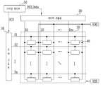
도 2를 참조하면, 본 발명의 실시예에 의한 발광 표시장치는 제 1주사선들(S11 내지 S1n), 제 2주사선들(S21 내지 S2n), 발광 제어선들(E1 내지 En) 및 데이터선들(D1 내지 Dm)에 의하여 구획된 영역에 형성되는 화소들(140)을 포함하는 화상 표시부(130)와, 제 1주사선들(S11 내지 S1n), 제 2주사선들(S21 내지 S2n) 및 발광 제어선들(E1 내지 En)을 구동하기 위한 주사 구동부(110)와, 데이터선들(D1 내지 Dm)을 구동하기 위한 데이터 구동부(120)와, 주사 구동부(110) 및 데이터 구동부(120)를 제어하기 위한 타이밍 제어부(150)를 구비한다.Referring to FIG. 2, a light emitting display device according to an exemplary embodiment of the present invention may include first scan lines S11 to S1n, second scan lines S21 to S2n, emission control lines E1 to En, and data lines D1. Through the
화상 표시부(130)는 제 1주사선들(S11 내지 S1n), 제 2주사선들(S21 내지 S2n), 발광 제어선들(E1 내지 En) 및 데이터선들(D1 내지 Dm)에 의하여 구획된 영역에 형성되는 화소들(140)을 구비한다. 화소들(140)은 외부로부터 제 1전원(VDD) 및 제 2전원(VSS)을 공급받는다. 제 1전원(VDD) 및 제 2전원(VSS)을 공급받은 화소들(140) 각각은 데이터선(D)으로부터 공급되는 데이터신호에 대응하여 제 1전원(VDD)으로부터 발광소자를 경유하여 제 2전원(VSS)으로 흐르는 픽셀전류를 제어한다. 그리고, 화소들(140)은 1 수평기간의 일부기간 동안 픽셀전류를 데이터선(D)을 경유하여 데이터 구동부(120)로 공급한다. 이를 위하여, 화소들(140) 각각은 도 3과 같이 구성될 수 있다. 도 3에 도시된 화소(140)의 상세한 구조는 후술하기로 한다.The
타이밍 제어부(150)는 외부로부터 공급되는 동기신호들에 대응하여 데이터 구동제어신호(DCS) 및 주사 구동제어신호(SCS)를 생성한다. 타이밍 제어부(150)에서 생성된 데이터 구동제어신호(DCS)는 데이터 구동부(120)로 공급되고, 주사 구동제어신호(SCS)는 주사 구동부(110)로 공급된다. 그리고, 타이밍 제어부(150)는 외부로부터 공급되는 데이터(Data)를 데이터 구동부(120)로 공급한다.The
주사 구동부(110)는 타이밍 제어부(150)로부터 주사 구동제어신호(SCS)를 공급받는다. 주사 구동제어신호(SCS)를 공급받은 주사 구동부(110)는 제 1주사선들(S11 내지 S1n)로 제 1주사신호를 순차적으로 공급함과 동시에 제 2주사선들(S21 내지 S2n)로 제 2주사신호를 순차적으로 공급한다.The
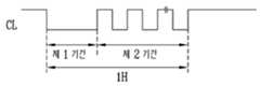
여기서, 주사 구동부(110)는 도 4에 도시된 바와 같이 1수평기간 중 제 1기간 동안 화소(140)의 제 1트랜지스터(M1)가 턴-온되고, 제 2기간 동안 제 1트랜지 스터(M1)가 턴-온 및 턴-오프를 반복하도록 제 1주사신호를 공급한다. 그리고, 주사 구동부(110)는 1수평기간 중 제 1기간 동안 화소(140)의 제 2트랜지스터(M2)가 턴-오프되고, 제 2기간 동안 제 1트랜지스터(M1)와 교번적으로 턴-온 및 턴-오프를 반복하도록 제 2주사신호를 공급한다. 또한, 주사 구동부(110)는 제 1주사신호 및 제 2주사신호가 공급되는 기간동안 제 3트랜지스터(M3)가 턴-오프되고, 그 외의 기간 동안 턴-온될 수 있도록 발광 제어신호를 공급한다. 즉, 발광 제어신호는 제 1주사신호 및 제 2주사신호와 중첩되게 공급되며, 그 폭은 제 1주사신호의 폭과 동일하거나 넓게 설정된다.As illustrated in FIG. 4, in the
데이터 구동부(120)는 타이밍 제어부(150)로부터 데이터 구동제어신호(DCS)를 공급받는다. 데이터 구동제어신호(DCS)를 공급받은 데이터 구동부(120)는 데이터신호를 생성하고, 생성된 데이터신호를 데이터선들(D1 내지 Dm)로 공급한다. 여기서, 데이터 구동부(120)는 데이터신호로써 소정의 계조전압을 데이터선들(D1 내지 Dm)로 공급한다.The
그리고, 데이터 구동부(120)는 제 2기간의 일부기간 동안 화소들(140)로부터 픽셀전류를 공급받고, 공급받은 픽셀전류가 데이터(Data)에 대응되는 전류값을 갖는지 체크한다. 예를 들어, 데이터(Data)의 비트수(또는 계조값)에 대응하여 화소(140)에서 흘러야 하는 픽셀전류가 10㎂인 경우 데이터 구동부(120)는 자신에게 공급되는 픽셀전류가 10㎂인지 체크한다. 여기서, 화소들(140) 각각에서 원하는 전류가 공급되지 않는 경우 데이터 구동부(120)는 화소들(140) 각각에서 원하는 전류가 흐를 수 있도록 계조전압을 변경한다. 이를 위해, 데이터 구동부(120)는 j(j는 자연수)개의 채널로 구성되는 적어도 하나 이상의 데이터 집적회로(129)를 구비한다. 데이터 집적회로(129)의 상세한 구성은 후술하기로 한다.In addition, the
도 3은 도 2에 도시된 화소의 제 1실시예를 나타내는 도면이다. 도 3에서는 설명의 편의성을 위하여 제 m데이터선(Dm), n번째 제 1주사선(S1n), n번째 제 2주사선(S2n) 및 제 n발광 제어선(En)과 접속된 화소를 도시하기로 한다. 그리고, 도 3에서 트랜지스터들(M1 내지 M4)이 피모스(PMOS) 도전형으로 도시되었지만, 본 발명이 이에 한정되는 것은 아니다.FIG. 3 is a diagram illustrating a first embodiment of the pixel illustrated in FIG. 2. In FIG. 3, pixels connected to the m-th data line Dm, the n-th first scan line S1n, the n-th second scan line S2n, and the n-th emission control line En are illustrated in FIG. 3. do. In addition, although the transistors M1 to M4 are illustrated in the PMOS conductivity type in FIG. 3, the present invention is not limited thereto.
도 3을 참조하면, 본 발명의 제 1실시예에 의한 화소(140)는 발광소자(OLED), 제 1스위칭블록(141), 제 2스위칭블록(142), 구동부(143) 및 제 3트랜지스터(M3)를 구비한다.Referring to FIG. 3, the
제 1스위칭블록(141)은 데이터선(Dm)과 구동부(143) 사이에 접속되어 데이터선(Dm)으로부터 공급되는 계조전압을 구동부(143)로 공급한다. 이를 위하여, 제 1스위칭블록(141)은 적어도 하나 이상의 트랜지스터를 구비한다. 예를 들어, 제 1스위칭블록(141)은 하나의 제 1트랜지스터(M1)를 구비할 수 있다. 제 1트랜지스터(M1)는 n번째 제 1주사선(S1n)으로부터 공급되는 제 1주사신호에 의하여 제어된다.The
제 2스위칭블록(142)은 구동부(143) 및 발광소자(OLED)의 공통단자와 데이터선(Dm) 사이에 접속되어 구동부(143)로부터 공급되는 픽셀전류를 데이터선(Dm)으로 공급한다. 이를 위하여, 제 2스위칭블록(142)은 적어도 하나 이상의 트랜지스터를 구비한다. 예를 들어, 제 2스위칭블록(142)은 하나의 제 2트랜지스터(M2)를 구비 할 수 있다. 제 2트랜지스터(M2)는 n번째 제 2주사선(S2n)으로부터 공급되는 제 2주사신호에 의하여 제어된다.The
제 3트랜지스터(M3)는 구동부(143)와 발광소자(OLED) 사이에 접속된다. 이와 같은 제 3트랜지스터(M3)는 제 n발광 제어선(En)으로부터 공급되는 발광 제어신호에 의하여 제어된다. 실제로, 제 3트랜지스터(M3)는 발광 제어신호가 공급될 때 턴-오프되고, 그 외의 기간 동안 턴-온된다.The third transistor M3 is connected between the driving
구동부(143)는 제 1트랜지스터(M1)로부터 공급되는 계조전압에 대응되는 픽셀전류를 제 2트랜지스터(M2) 및 제 3트랜지스터(M3)로 공급한다. 이를 위해, 구동부(143)는 제 1전원(VDD)과 제 3트랜지스터(M3) 사이에 접속되는 제 4트랜지스터(M4)와, 제 4트랜지스터(M4)의 게이트전극과 제 1전원(VDD) 사이에 접속되는 제 1커패시터(C1)를 구비한다. 제 1커패시터(C1)는 계조전압에 대응되는 소정의 전압을 충전한다. 제 4트랜지스터(M4)는 제 1커패시터(C1)에 충전된 전압에 대응하여 픽셀전류를 공급한다.The
도 3 및 도 4를 참조하여 화소(140)의 동작과정을 상세히 설명하면, 먼저 한 프레임의 특정 수평기간 동안 n번째 제 1주사선(S1n)으로 제 1주사신호가 공급됨과 동시에 n번째 제 2주사선(S2n)으로 제 2주사신호가 공급된다.Referring to FIGS. 3 and 4, the operation of the
제 1주사신호를 공급받은 제 1트랜지스터(M1)는 1수평기간 중 제 1기간 동안 턴-온된다. 제 1트랜지스터(M1)가 턴-온되면 제 1기간 동안 데이터선(Dm)으로 공급되는 데이터신호(계조전압)가 제 1커패시터(C1)로 공급된다. 이때, 제 1커패시터(C1)에는 데이터신호에 대응되는 소정의 전압이 충전된다. 한편, 제 2주사신호 를 공급받은 제 2트랜지스터(M2)는 제 1기간 동안 턴-오프 상태를 유지한다.The first transistor M1 supplied with the first scan signal is turned on for the first period of one horizontal period. When the first transistor M1 is turned on, the data signal (gradation voltage) supplied to the data line Dm is supplied to the first capacitor C1 during the first period. At this time, the first capacitor C1 is charged with a predetermined voltage corresponding to the data signal. Meanwhile, the second transistor M2 supplied with the second scan signal maintains the turn-off state for the first period.
이후, 제 2기간의 일부기간 동안 제 1트랜지스터(M1)가 턴-오프되고, 제 2트랜지스터(M2)가 턴-온된다. 제 2트랜지스터(M2)가 턴-온되면 제 1커패시터(C1)에 충전된 소정의 전압에 대응하여 제 4트랜지스터(M4)로부터 공급되는 픽셀전류가 데이터선(Dm)으로 공급된다. 데이터선(Dm)으로 공급된 픽셀전류는 데이터 구동부(120)로 공급되고, 픽셀전류를 공급받은 데이터 구동부(120)는 화소(140)에서 원하는 픽셀전류가 흐를 수 있도록 계조전압의 전압값을 증감시킨다. 이후, 제 2트랜지스터(M2)가 턴-오프되고, 제 1트랜지스터(M1)가 턴-온된다. 제 1트랜지스터(M1)가 턴-온되면 데이터 구동부(120)에서 증감된 계조전압이 제 1커패시터(C1)로 공급되어 제 1커패시터(C1)의 충전 전압값이 변화된다. 실제로, 제 2기간 동안에 제 1트랜지스터(M1) 및 제 2트랜지스터(M2)는 교번적으로 적어도 한번 이상 턴-온 및 턴-오프되면서 원하는 픽셀전류가 흐를 수 있도록 제 1커패시터(C1)의 충전 전압값을 변화시킨다.Thereafter, the first transistor M1 is turned off and the second transistor M2 is turned on for a part of the second period. When the second transistor M2 is turned on, the pixel current supplied from the fourth transistor M4 is supplied to the data line Dm in response to a predetermined voltage charged in the first capacitor C1. The pixel current supplied to the data line Dm is supplied to the
도 5는 도 2에 도시된 데이터 집적회로를 상세히 나타내는 도면이다. 도 5는 설명의 편의성의 위하여 데이터 집적회로(129)가 j개의 채널을 갖는다고 가정하기로 한다.FIG. 5 is a diagram illustrating in detail the data integrated circuit shown in FIG. 2. FIG. 5 assumes that the data integrated
도 5를 참조하면, 데이터 집적회로(129)는 샘플링 신호를 순차적으로 생성하기 위한 쉬프트 레지스터부(200)와, 샘플링 신호에 응답하여 데이터(Data)를 순차적으로 저장하기 위한 샘플링 래치부(210)와, 샘플링 래치부(210)의 데이터(Data) 들을 일시 저장함과 아울러 저장된 데이터(Data)들을 전압 디지털-아날로그 변환부(이하, "VDAC부"라 함)(230) 및 전류 디지털-아날로그 변환부(이하 "IDAC부"라 함)(240)로 공급하기 위한 홀딩 래치부(220)와, 데이터(Data)의 계조값에 대응하여 계조전압(Vdata)을 생성하는 VDAC부(230)와, 데이터(Data)의 계조값에 대응하여 계조전류(Idata)를 생성하는 IDAC부(240)와, 데이터선들(D1 내지 Dj)로부터 공급되는 픽셀전류(Ipixel)에 대응하여 계조전압(Vdata)을 변경시키기 위한 전압 조정블록(250)과, 전압 조정블록(250)으로부터 공급되는 계조전압(Vdata)을 데이터선들(D1 내지 Dj)로 공급하기 위한 버퍼부(260)와, 데이터선들(D1 내지 Dj)을 버퍼부(260) 및 전압 조정블록(250) 중 어느 하나와 선택적으로 접속시키기 위한 선택블록(280)을 구비한다.Referring to FIG. 5, the data integrated
쉬프트 레지스터부(200)는 타이밍 제어부(150)로부터 소스 쉬프트 클럭(SSC) 및 소스 스타트 펄스(SSP)를 공급받는다. 소스 쉬프트 클럭(SSC) 및 소스 스타트 펄스(SSP)를 공급받은 쉬프트 레지스터부(200)는 소스 쉬프트 클럭(SSC)의 1주기 마다 소스 스타트 펄스(SSP)를 쉬프트 시키면서 순차적으로 j개의 샘플링신호를 생성한다. 이를 위해, 쉬프트 레지스터부(200)는 j개의 쉬프트 레지스터(2001 내지 200j)를 구비한다.The
샘플링 래치부(210)는 쉬프트 레지스터(200)로부터 순차적으로 공급되는 샘플링신호에 응답하여 데이터(Data)를 순차적으로 저장한다. 여기서, 샘플링 래치부(210)는 j개의 데이터(Data)를 저장하기 위하여 j개의 샘플링 래치(2101 내지 210j)를 구비한다. 그리고, 각각의 샘플링 래치들(2101 내지 210j)은 데이터 (Data)의 비트수에 대응되는 크기를 갖는다. 예를 들어, 데이터(Data)들이 k비트로 구성되는 경우 샘플링 래치(2101 내지 210j) 각각은 k비트의 크기로 설정된다.The
홀딩 래치부(220)는 소스 출력 인에이블(SOE) 신호가 입력될 때 샘플링 래치부(210)로부터 데이터(Data)를 입력받아 저장한다. 그리고, 홀딩 래치부(220)는 소스 출력 인에이블(SOE) 신호가 입력될 때 자신에게 저장된 데이터(Data)를 VDAC부(230) 및 IDAC부(240)로 공급한다. 이를 위해, 홀딩 래치부(220)는 k비트로 설정된 j개의 홀딩 래치(2201 내지 220j)를 구비한다.The holding
VDAC부(230)는 데이터(Data)의 비트값(즉, 계조값)에 대응하여 계조전압(Vdata)을 생성하고, 생성된 계조전압(Vdata)을 전압 조정블록(250)으로 공급한다. 여기서, VDAC부(230)는 홀딩 래치부(220)로부터 공급되는 j개의 데이터(Data)에 대응하여 j개의 계조전압(Vdata)을 생성한다. 이를 위해, VDAC부(230)는 j개의 전압 생성부(2301 내지 230j)를 구비한다. 이후, 설명의 편의성을 위하여 VDAC부(230)에서 생성된 계조전압(Vdata)을 제 1계조전압(Vdata)이라 부르기로 한다.The
IDAC부(240)는 데이터(Data)의 비트값에 대응하여 계조전류(Idata)를 생성하고, 생성된 계조전류(Idata)를 전압 조정블록(250)로 공급한다. 여기서, IDAC부(240)는 홀딩 래치부(220)로부터 공급되는 j개의 데이터(Data)에 대응하여 j개의 계조전류(Idata)를 생성한다. 이를 위해, IDAC부(240)는 j개의 전류 생성부(2401 내지 240j)를 구비한다.The
전압 조정블록(250)은 제 1계조전압(Vdata), 계조전류(Idata) 및 픽셀전류(Ipixel)를 공급받는다. 제 1계조전압(Vdata), 계조전류(Idata) 및 픽셀전류 (Ipixel)를 공급받은 전압 조정블록(250)은 계조전류(Idata)와 픽셀전류(Ipixel)의 전류차를 비교하고, 비교된 전류차에 대응되어 제 1계조전압(Vdata)의 전압값을 재조정한다. 이후, 설명의 편의성을 위하여 전압 조정블록(250)에서 재조정된 제 1계조전압(Vdata)을 제 2계조전압으로 부르기로 한다. 이상적으로 전압 조정블록(250)은 계조전류(Idata)와 픽셀전류(Ipixel)가 동일한 값으로 설정될 수 있도록 제 2계조전압의 전압값을 제어한다. 이를 위하여, 전압 조정블록(250)은 j개의 전압 조정부(2501 내지 250j)를 구비한다.The
버퍼부(260)는 전압 조정블록(250)으로부터 공급되는 제 1계조전압(Vdata) 또는 제 2계조전압을 j개의 데이터선들(D1 내지 Dj)로 공급한다. 이를 위해, 버퍼부(260)는 j개의 버퍼(2601 내지 260j)를 구비한다.The
선택블록(280)은 데이터선들(D1 내지 Dj)을 버퍼부(260) 또는 전압 조정블록(250)과 선택적으로 접속시킨다. 이를 위해, 선택블록(280)은 j개의 선택부(2801 내지 280j)를 구비한다.The
한편, 본 발명의 데이터 집적회로는 도 6과 같이 홀딩 래치부(220)와 VDAC부(230) 및 IDAC부(240)의 사이에 레벨 쉬프터부(270)를 더 포함할 수 있다. 레벨 쉬프터부(270)는 홀딩 래치부(220)로부터 공급되는 데이터(Data)의 전압레벨을 상승시켜 VDAC부(230) 및 IDAC부(240)로 공급한다. 외부 시스템으로부터 데이터 집적회로(129)로 높은 전압레벨을 가지는 데이터(Data)가 공급되면 전압레벨에 대응되는 회로 부품들이 설치되어야 하기 때문에 제조비용이 증가된다. 따라서, 데이터 집적회로(129)외부에서는 낮은 전압레벨을 가지는 데이터(Data)를 공급하고, 이 낮은 전압레벨을 가지는 데이터(Data)를 레벨 쉬트터부(270)에서 높은 전압레벨로 승압시킨다.Meanwhile, the data integrated circuit of the present invention may further include a
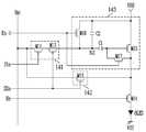
도 7은 도 4에 도시된 전압 조정부 및 선택부를 상세히 나타내는 도면이다. 도 7에서는 설명의 편의성을 위하여 j번째 전압 조정부(250j) 및 선택부(280j)를 도시하기로 한다.FIG. 7 is a detailed diagram illustrating the voltage adjusting unit and the selecting unit illustrated in FIG. 4. In FIG. 7, for convenience of description, the j-
도 7을 참조하면, 본 발명의 선택부(280j)는 버퍼(260j)와 데이터선(Dj) 사이에 접속되는 제 5트랜지스터(M5)와, 전압 조정부(250j)와 데이터선(Dj) 사이에 접속되는 제 6트랜지스터(M6)를 구비한다. 제 5트랜지스터(M5) 및 제 6트랜지스터(M6)는 교번적으로 턴-온되면서 데이터선(Dj)을 버퍼(260j) 및 전압 조정부(250j) 중 어느 하나와 접속시킨다. 이를 위해, 제 5트랜지스터(M5) 및 제 6트랜지스터(M6)는 서로 다른 도전형으로 설정된다. 그리고, 제 5트랜지스터(M5) 및 제 6트랜지스터(M6)는 제어라인(CL)으로부터 공급되는 선택신호에 의하여 제어된다.Referring to FIG. 7, the
선택신호는 도 8에 도시된 바와 같이 1수평기간 중 제 1기간 동안 제 5트랜지스터(M5)가 턴-온될 수 있도록 공급된다. 그리고, 선택신호는 제 2기간 동안 제 5트랜지스터(M5) 및 제 6트랜지스터(M6)가 교번적으로 턴-온되도록 공급된다. 실제로, 선택신호는 제 2기간 동안 제 1트랜지스터(M1)와 동일하게 제 5트랜지스터(M5)가 턴-온 및 턴-오프되며, 제 2트랜지스터(M2)와 동일하게 제 6트랜지스터(M6)가 턴-온 및 턴-오프되록 공급된다.As shown in FIG. 8, the selection signal is supplied such that the fifth transistor M5 can be turned on during the first period of one horizontal period. The selection signal is supplied to alternately turn on the fifth transistor M5 and the sixth transistor M6 during the second period. In practice, the selection signal is turned on and turned off in the fifth transistor M5 in the same manner as the first transistor M1 during the second period, and the sixth transistor M6 in the same manner as the second transistor M2. Supplied to be turned on and off.
전압 조정부(250j)는 비교부(252), 전압 증감부(254), 제어부(256), 커패시 터(C) 및 스위칭소자(SW1)를 구비한다. 스위칭소자(SW1)는 VDAC부(230)와 버퍼(260j) 사이에 설치된다. 이와 같은 스위칭소자(SW1)는 제어부(256)의 제어에 의하여 제 1기간 동안 턴-온되고, 제 2기간 동안 턴-오프된다.The
커패시터(C)는 스위칭소자(SW1)와 버퍼(260j)의 공통단자인 제 1노드(N1)와 전압 증감부(254) 사이에 설치된다. 제 1노드(N1)와 전압 증감부(254) 사이에 설치된 커패시터(C)는 전압 증감부(254)로부터 공급되는 전압에 대응하여 제 1노드(N1)의 전압값을 증감시킨다. 즉, 전압 증감부(254)에서 높은 전압이 공급되면 커패시터(C)에 의하여 제 1노드(N1)의 전압값이 증가되고, 전압 증감부(254)에서 낮은 전압이 공급되면 커패시터(C)에 의하여 제 1노드(N1)의 전압값이 감소된다.The capacitor C is provided between the first node N1, which is a common terminal of the switching element SW1, and the
비교부(252)는 IDAC부(240)로부터 계조전류(Idata)를 공급받고, 데이터선(Dj) 및 선택부(280j)를 경유하여 화소(140)로부터 픽셀전류(Ipixel)를 공급받는다. 따라서, 픽셀전류(Ipixel)는 현재 제 1 및 제 2주사신호가 공급되는 화소(140)로부터 공급된다. 픽셀전류(Ipixel) 및 계조전류(Idata)를 공급받은 비교부(252)는 계조전류(Idata)와 픽셀전류(Ipixel)를 비교하고, 비교된 결과에 대응하는 제 1제어신호 또는 제 2제어신호를 전압 증감부(254)로 공급한다. 예를 들어, 비교부(252)는 계조전류(Idata)가 픽셀전류(Ipixel)보다 큰 경우 제 1제어신호를 생성하고, 계조전류(Idata)가 픽셀전류(Ipixel)보다 작은 경우 제 2제어신호를 생성하여 전압 증감부(254)로 공급한다.The
전압 증감부(254)는 비교부(252)로부터 공급되는 제 1제어신호 또는 제 2제어신호에 대응되어 소정의 전압값을 커패시터(C)로 공급한다. 여기서, 전압 증감 부(254)는 픽셀전류(Ipixel) 및 계조전류(Idata)가 유사해질 수 있도록 소정의 전압을 커패시터(C)로 공급한다. 그러면, 제 1노드(N1)의 전압값은 커패시터(C)로 공급된 전압에 대응되어 증가 또는 감소된다. 여기서, 증가 또는 감소된 제 1노드(N1)의 전압은 제 2계조전압으로 이용된다.The voltage increasing / decreasing
제어부(256)는 1수평기간(1H) 중 제 1기간 동안 스위칭소자(SW1)를 턴-온시키고, 제 2기간 동안 스위칭소자(SW1)를 턴-오프시킨다. 그리고, 제어부(256)는 제 2기간 동안 서서히 증가되는 카운팅신호를 전압 증감부(254)로 공급된다. 예를 들어, 제어부(256)는 "1"로부터 "l"(l은 자연수)까지 증가되는 카운팅신호를 전압 증감부(254)로 공급한다. 이를 위하여, 제어부(256)의 내부에는 도시되지 않은 카운터가 포함된다. 제어부(256)의 카운팅신호는 리셋신호(Reset)가 공급될 때 초기화된다. 여기서, 리셋신호(Reset)는 1수평기간 단위로 공급되는 신호로 설정된다. 예를 들어, 리셋신호(Reset)는 수평 동기신호(H) 또는 주사신호 등으로 이용될 수 있다.The
동작과정을 상세히 설명하면, 먼저 1수평기간의 제 1기간 동안 스위칭소자(SW1), 제 5트랜지스터(M5) 및 제 1트랜지스터(M1)가 턴-온된다. 스위칭소자(SW1)가 턴-온되면 VDAC부(230)로부터 공급되는 제 1계조전압(Vdata)이 버퍼(260j) 및 제 5트랜지스터(M5)를 경유하여 데이터선(Dj)으로 공급된다. 데이터선(Dj)으로 공급된 제 1계조전압(Vdata)은 주사신호에 의해 선택된 화소(140)로 공급된다. 즉, 데이터선(Dj)으로 공급된 제 1계조전압(Vdata)은 제 1주사신호에 의하여 턴-온된 제 1트랜지스터(M1)를 경유하여 구동부(142)로 공급된다. 그러면, 구동부(142)에 포함된 제 1커패시터(C1)에 제 1계조전압(Vdata)에 대응되는 전압이 충전된다. 실제로, 제 1기간은 화소(140)에 포함된 제 1커패시터(C1)에 제 1계조전압(Vdata)에 대응되는 소정의 전압이 충전되도록 그 기간이 설정된다.In detail, the switching device SW1, the fifth transistor M5, and the first transistor M1 are turned on during the first period of one horizontal period. When the switching device SW1 is turned on, the first gray voltage Vdata supplied from the
화소(140)에 포함된 제 1커패시터(C1)에 소정의 전압이 충전된 후 제 2기간의 시작될 때 제 6트랜지스터(M6) 및 제 2트랜지스터(M2)가 턴-온되고, 스위칭소자(SW1), 제 5트랜지스터(M5) 및 제 1트랜지스터(M1)가 턴-오프된다. 스위칭소자(SW1)가 턴-오프되면 제 1노드(N1)가 플로팅된다. 이때, 제 1노드(N1)는 도시되지 않는 기생 커패시터 등에 의하여 제 1계조전압(Vdata)의 전압을 유지한다. 제 2트랜지스터(M2)가 턴-온되면 화소(140)의 구동부(142)에서 생성된 픽셀전류(Ipixel)가 제 2트랜지스터(M2), 데이터선(Dj) 및 제 6트랜지스터(M6)를 경유하여 비교부(252)로 공급된다.After the predetermined voltage is charged in the first capacitor C1 included in the
픽셀전류(Ipixel)를 공급받은 비교부(252)는 IDAC부(240)로부터 공급되는 계조전류(Idata)와 픽셀전류(Ipixel)를 비교하고, 비교결과에 대응하여 제 1제어신호 또는 제 2제어신호를 생성하여 전압 증감부(254)로 공급한다. 여기서, 계조전류(Idata)는 데이터(data)에 대응하여 화소(140)에서 실제로 흘러야되는 이상적인 전류값이고, 픽셀전류(Ipixel)는 화소(140)에서 실제 흐르는 전류값이다.The
제 2기간 동안 제어부(256)는 "1"로부터 "l"까지 증가되는 카운팅신호를 전압 증감부(254)로 공급한다. 카운팅신호를 공급받은 전압 증감부(254)는 비교부(252)로부터 공급되는 제 1제어신호 또는 제 2제어신호에 대응하여 제 1커패시터(C1)로 소정의 전압값을 공급한다. 여기서, 전압 증감부(254)는 제 1제어신호 또 는 제 2제어신호에 대응하여 계조전류(Idata)와 픽셀전류(Ipixel)가 동일 또는 유사해질 수 있도록 커패시터(C)로 공급되는 전압값을 제어한다. 그러면, 제 1노드(N1)의 전압값이 커패시터(C)로 공급되는 전압값에 대응하여 변화되면서 제 2계조전압이 생성된다.During the second period, the
제 2계조전압이 생성된 후 제 6트랜지스터(M6) 및 제 2트랜지스터(M2)가 턴-오프되고, 제 5트랜지스터(M5) 및 제 1트랜지스터(M1)가 턴-온된다. 제 5트랜지스터(M5) 및 제 1트랜지스터(M1)가 턴-온되면 제 1노드(N1)에 인가된 제 2계조전압이 화소(140)로 공급된다. 그러면, 화소(140)에서는 제 2계조전압에 대응되는 픽셀전류(Ipixel)가 생성된다. 실제로, 본 발명에서는 제 2기간 동안 계조전류(Idata)와 픽셀전류(Ipixel)가 유사 또는 동일해지도록 제 6 및 제 2트랜지스터(M2,M6)와, 제 5 및 제 1트랜지스터(M1,M5)가 교번적으로 적어도 한번 이상 턴-온 및 턴-오프된다.After the second gray voltage is generated, the sixth transistor M6 and the second transistor M2 are turned off, and the fifth transistor M5 and the first transistor M1 are turned on. When the fifth transistor M5 and the first transistor M1 are turned on, the second gray voltage applied to the first node N1 is supplied to the
한편, 전압 증감부(254)에서 증감되는 전압범위는 카운팅신호에 의하여 결정된다. 예를 들어, 전압 증감부(254)는 첫번째 카운팅신호(예를 들면, "1")가 공급될 때 도 9와 같이 제 1전압(V1)의 범위내에서 전압을 증감한다. 다시 말하여, 첫번째 카운팅신호가 공급되면 V1/2의 전압이 증가 또는 감소된다. 그리고, 전압 증감부(254)는 두번째 카운팅신호(예를 들면, "2")가 공급될 때 제 1전압(V1)보다 낮은 제 2전압(V2)의 범위내에서 전압을 증감한다. 다시 말하여, 두번째 카운팅신호가 공급되면 V2/2의 전압이 증가 또는 감소된다. 한편, 제 2전압(V2)은 제 1전압(V1)의 대략 1/2로 설정된다. 그리고, 전압 증감부(254)는 세번째 카운팅신호( 예를 들면, "3")가 공급될 때 제 2전압(V2)보다 낮은 제 3전압(V3)의 범위내에서 전압을 증감한다. 즉, 카운팅신호가 증가될 수록 전압 증감부(254)에서 증감되는 전압범위는 낮아진다. 여기서, 낮아지는 전압범위는 이전 전압범위의 1/2로 설정될 수 있다. 이와 같은 방식으로 전압 증감부(254)는 계조전압(Idata) 및 픽셀전류(Ipixel)가 동일 또는 유사해질 수 있도록 제 1커패시터(C1)로 공급되는 전압을 제어한다.On the other hand, the voltage range which is increased or decreased in the voltage increase /
한편, 도 3에 도시된 화소(140)의 구동부(143)는 제 4트랜지스터(M4)의 문턱전압을 보상할 수 없다. 다시 말하여, 원하는 전압값을 가지는 데이터신호(제 1계조전압 또는 제 2계조전압)가 공급되더라도 제 4트랜지스터(M4)의 문턱전압 만큼 데이터신호의 전압값이 변화된다. 따라서, 화소(140)의 구동부(143)가 도 3에 도시된 바와 같이 구성되면 화소(140)에서 원하는 픽셀전류(Ipixel)가 흐르기까지 많은 시간이 소비된다. 다시 말하여, 화소(140)의 구동부(143)가 도 3과 같이 구성되면 1수평기간의 제 2기간 동안 화소에서(140)에서 원하는 픽셀전류(Ipixel)가 흐르지 못할 염려가 있다. 이와 같은 문제점을 극복하기 위하여 본 발명에서는 도 10과 같이 트랜지스터의 문턱전압과 무관하게 픽셀전류(Ipixel)를 생성할 수 있는 화소(140)를 제안한다.Meanwhile, the
도 10은 본 발명의 제 2실시예에 의한 화소를 나타내는 도면이다. 도 10에서는 설명의 편의성을 위하여 제 m데이터선(Dm), n번째 제 1주사선(S1n), n번째 제 2주사선(S2n) 및 제 n발광 제어선(En)과 접속된 화소를 도시하기로 한다.10 is a diagram illustrating a pixel according to a second exemplary embodiment of the present invention. In FIG. 10, pixels connected to the m-th data line Dm, the n-th first scan line S1n, the n-th second scan line S2n, and the n-th emission control line En are illustrated in FIG. 10. do.
도 10을 참조하면, 본 발명의 제 2실시예에 의한 화소(140)는 발광소자(OLED), 제 1스위칭블록(141), 제 2스위칭블록(142), 구동부(143) 및 제 4트랜지스터(M14)를 구비한다.Referring to FIG. 10, the
제 1스위칭블록(141)은 데이터선(Dm)과 구동부(143) 사이에 접속되어 데이터선(Dm)으로부터 공급되는 데이터신호(제 1계조전압 또는 제 2계조전압)를 구동부(143)로 공급한다. 이를 위하여, 제 1스위칭블록(141)은 제 1트랜지스터(M11)를 구비한다. 제 1트랜지스터(M11)는 데이터선(Dm)과 구동부(143) 사이에 접속된다. 이와 같은 제 1트랜지스터(M11)는 n번째 제 1주사선(S1n)으로 공급되는 제 1주사신호에 의하여 제어된다. 즉, 제 1트랜지스터(M11)는 1수평기간 중 제 1기간 동안 턴-온되고, 제 2기간 동안 적어도 한번 이상 턴-온 및 턴-오프된다.The
제 2스위칭블록(142)은 데이터선(Dm)과 구동부(143) 사이에 접속되어 구동부(143)로부터 공급되는 픽셀전류를 데이터선(Dm)으로 공급한다. 이를 위해, 제 2스위칭블록(142)은 제 3트랜지스터(M13)를 구비한다. 제 3트랜지스터(M13)는 n번째 제 2주사선(S2n)으로부터 공급되는 제 2주사신호에 의하여 제어된다. 즉, 제 3트랜지스터(M13)는 1수평기간 중 제 1기간 동안 턴-오프되고, 제 2기간 동안 제 1트랜지스터(M11)와 교번적으로 턴-온 및 턴-오프된다.The
제 4트랜지스터(M14)는 구동부(143)와 발광소자(OLED) 사이에 접속된다. 이와 같은 제 4트랜지스터(M14)는 제 n발광 제어선(En)으로부터 공급되는 발광 제어신호에 의하여 제어된다. 발광 제어신호는 제 1주사신호 및 제 2주사신호와 중첩되게 공급되며, 그 폭은 제 1주사신호와 동일하거나 넓게 설정된다. 제 4트랜지스 터(M14)는 발광 제어신호가 공급될 때 턴-오프되고, 그 외의 기간 동안 턴-온된다.The fourth transistor M14 is connected between the driving
구동부(143)는 제 1스위칭블록(141)으로부터 공급되는 데이터신호에 대응되는 픽셀전류(Ipixel)를 제 2스위칭블록(142) 및 제 4트랜지스터(M14)로 공급한다. 여기서, 구동부(143)는 제 5트랜지스터(M15)의 문턱전압을 보상할 수 있는 구조를 갖는다. 예를 들어, 구동부(143)는 현재 공지되어 트랜지스터의 문턱전압을 보상할 수 있는 다양한 회로들 중 어느 하나로 선택될 수 있다.The
구동부(143)는 제 1커패시터(C1), 제 2커패시터(C2), 제 5트랜지스터(M15), 제 6트랜지스터(M16) 및 제 7트랜지스터(M17)를 구비한다. 제 1커패시터(C1)는 제 5트랜지스터(M15)와 제 1스위칭블록(M11) 사이에 접속된다. 이와같은 제 1커패시터(C1)는 제 5트랜지스터(M15)의 문턱전압에 대응하는 전압을 충전한다.The driving
제 2커패시터(C2)는 제 1커패시터(C1)와 제 1스위칭블록(M11)의 공통단자인 제 2노드(N2)와 제 1전원(VDD) 사이에 접속된다. 이와 같은 제 2커패시터(C2)는 데이터신호에 대응되는 전압을 충전한다.The second capacitor C2 is connected between the second node N2, which is a common terminal of the first capacitor C1, and the first switching block M11, and the first power source VDD. The second capacitor C2 charges a voltage corresponding to the data signal.
제 5트랜지스터(M15)는 제 1전원(VDD)과 제 4트랜지스터(M14) 사이에 접속된다. 이와 같은 제 5트랜지스터(M15)는 제 1커패시터(C1) 및 제 2커패시터(C2)에 충전된 전압에 대응되는 픽셀전류(Ipixel)를 제 2스위칭블록(142) 및 제 4커패시터(M14)로 공급한다.The fifth transistor M15 is connected between the first power source VDD and the fourth transistor M14. The fifth transistor M15 transfers the pixel current Ipixel corresponding to the voltage charged in the first capacitor C1 and the second capacitor C2 to the
제 6트랜지스터(M16)는 제 2노드(N2)와 제 1전원(VDD) 사이에 접속된다. 이와 같은 제 6트랜지스터(M16)는 제 n-1발광 제어선(En-1)으로부터 공급되는 발광 제어신호에 의하여 제어된다. 여기서, 제 6트랜지스터(M16)는 발광 제어신호가 공 급될 때 턴-온되고, 그 외의 기간에는 턴-오프된다. 이를 위해, 제 6트랜지스터(M16)는 제 4트랜지스터(M14)와 다른 도전형으로 형성된다. 예를 들어, 제 4트랜지스터(M14)가 피모스(PMOS) 도전형으로 형성되면 제 6트랜지스터(M16)는 엔모스(NMOS) 도전형으로 형성되고, 제 4트랜지스터(M14)가 엔모스(NMOS) 도전형으로 형성되면 제 6트랜지스터(M16)는 피모스(PMOS) 도전형으로 형성된다.The sixth transistor M16 is connected between the second node N2 and the first power source VDD. The sixth transistor M16 is controlled by the emission control signal supplied from the n-th emission control line En-1. Here, the sixth transistor M16 is turned on when the light emission control signal is supplied, and is turned off in other periods. To this end, the sixth transistor M16 is formed in a different conductivity type from the fourth transistor M14. For example, if the fourth transistor M14 is formed of PMOS conductive type, the sixth transistor M16 is formed of NMOS conductive type, and the fourth transistor M14 is formed of NMOS. The sixth transistor M16 is formed of a PMOS conductive type.
제 7트랜지스터(M17)는 제 5트랜지스터(M15)의 게이트전극과 제 2전극 사이에 접속된다. 이와 같은 제 7트랜지스터(M17)는 제 n-1발광 제어선(En-1)으로부터 공급되는 발광 제어신호에 의하여 제어된다. 여기서, 제 7트랜지스터(M17)는 발광 제어신호가 공급될 때 턴-온되고, 그 외의 기간에는 턴-오프된다. 이를 위해, 제 7트랜지스터(M17)는 제 6트랜지스터(M16)와 동일한 도전형으로 형성된다.The seventh transistor M17 is connected between the gate electrode and the second electrode of the fifth transistor M15. The seventh transistor M17 is controlled by the emission control signal supplied from the n-th emission control line En-1. Here, the seventh transistor M17 is turned on when the light emission control signal is supplied, and is turned off during other periods. To this end, the seventh transistor M17 is formed of the same conductivity type as the sixth transistor M16.
도 11은 도 10에 도시된 화소로 공급되는 주사신호를 나타내는 도면이다. 이후, 발광 제어신호는 대략 2수평기간의 폭으로 설정되며, n-1번째 발광 제어선으로 공급된 발광 제어신호와 n번째 발광 제어선으로 공급된 발광 제어신호는 1수평기간 만큼 중첩된다고 가정하여 설명하기로 한다.FIG. 11 is a diagram illustrating a scan signal supplied to the pixel illustrated in FIG. 10. Thereafter, the emission control signal is set to a width of approximately 2 horizontal periods, and it is assumed that the emission control signal supplied to the n-1th emission control line and the emission control signal supplied to the nth emission control line overlap by one horizontal period. Let's explain.
도 11을 참조하면, 먼저 k-1(k는 자연수)번째 수평기간(k-1H) 동안 제 n-1발광 제어선(En-1) 및 제 n발광 제어선(En)으로 발광 제어신호가 공급된다.Referring to FIG. 11, first, a light emission control signal is transmitted to an n-1th emission control line En-1 and an nth emission control line En during a k-1 (k is a natural number) horizontal period k-1H. Supplied.
제 n발광 제어선(En)으로 발광 제어신호가 공급되면 제 4트랜지스터(M14)가 턴-오프된다. 제 n-1발광 제어선(En-1)으로 발광 제어신호가 공급되면 제 6트랜지스터(M16) 및 제 7트랜지스터(M7)가 턴-온된다. 제6트랜지스터(M16)가 턴-온되면 제 2노드(N2)로 제 1전원(VDD)의 전압이 인가된다. 제 7트랜지스터(M17)가 턴-온되면 제 5트랜지스터(M15)가 다이오드 형태로 접속된다. 그러면, 제 5트랜지스터(M15)의 게이트단자로 제 1전원(VDD)에서 제 5트랜지스터(M15)의 문턱전압을 감한 전압이 인가된다. 이때, 제 1커패시터(C1)에는 제 5트랜지스터(M15)의 문턱전압이 충전된다.When the emission control signal is supplied to the nth emission control line En, the fourth transistor M14 is turned off. When the emission control signal is supplied to the n-th emission control line En-1, the sixth transistor M16 and the seventh transistor M7 are turned on. When the sixth transistor M16 is turned on, the voltage of the first power source VDD is applied to the second node N2. When the seventh transistor M17 is turned on, the fifth transistor M15 is connected in the form of a diode. Then, a voltage obtained by subtracting the threshold voltage of the fifth transistor M15 from the first power supply VDD is applied to the gate terminal of the fifth transistor M15. At this time, the threshold voltage of the fifth transistor M15 is charged to the first capacitor C1.
이후, 제 k번째 수평기간(kH) 동안 n번째 제 1주사선(S1n)으로 제 1주사신호가 공급되고, n번째 제 2주사선(S2n)으로 제 2주사신호가 공급된다. 그리고, k번째 수평기간(kH) 동안 제 n번째 발광 제어선(En)으로 발광 제어신호가 공급되고, n-1번째 발광 제어선(En)으로 발광 제어신호가 공급되지 않는다.Thereafter, the first scan signal is supplied to the nth first scan line S1n and the second scan signal is supplied to the nth second scan line S2n during the kth horizontal period kH. The light emission control signal is supplied to the nth light emission control line En and the light emission control signal is not supplied to the n−1th light emission control line En during the kth horizontal period kH.
제 1주사신호가 공급되면 제 1기간 동안 제 1트랜지스터(M11)가 턴-온된다. 제 1트랜지스터(M11)가 턴-온되면 제 1기간 동안 데이터선(Dm)으로 공급되는 데이터신호(제 1계조전압)가 제 2노드(N2)로 공급된다. 이때, 제 2커패시터(C2)에는 데이터신호에 대응되는 전압이 충전된다. 한편, 제 2주사신호를 공급받는 제 3트랜지스터(M13)는 제 1기간 동안 턴-오프된다.When the first scan signal is supplied, the first transistor M11 is turned on for the first period. When the first transistor M11 is turned on, the data signal (first gray voltage) supplied to the data line Dm is supplied to the second node N2 during the first period. At this time, the second capacitor C2 is charged with a voltage corresponding to the data signal. Meanwhile, the third transistor M13 supplied with the second scan signal is turned off for the first period.
이후, 제 2기간의 일부기간 동안 제 1트랜지스터(M11)가 턴-오프되고, 제 3트랜지스터(M13)가 턴-온된다. 제 3트랜지스터(M13)가 턴-온되면 제 1커패시터(C1) 및 제 2커패시터(C2)에 충전된 전압에 대응하여 제 5트랜지스터(M15)로부터 공급되는 픽셀전류(Ipixel)가 제 3트랜지스터(M13)를 경유하여 데이터선(Dm)으로 공급된다. 데이터선(Dm)으로 공급된 픽셀전류(Ipixel)는 데이터 집적회로(129)로 공급되고, 픽셀전류(Ipixel)를 공급받은 데이터 집적회로(129)는 화소(140)에서 원 하는 픽셀전류(Ipixel)가 흐를 수 있도록 데이터신호의 전압값을 증감시킨다. 그리고, 데이터 집적회로(129)는 증감된 전압값을 가지는 데이터신호(제 2계조전압)를 데이터선(Dm)으로 공급한다.Thereafter, the first transistor M11 is turned off and the third transistor M13 is turned on for a part of the second period. When the third transistor M13 is turned on, the pixel current Ipixel supplied from the fifth transistor M15 corresponds to the voltage charged in the first capacitor C1 and the second capacitor C2 and the third transistor M13 is turned on. It is supplied to the data line Dm via M13). The pixel current Ipixel supplied to the data line Dm is supplied to the data integrated
이후, 제 3트랜지스터(M3)가 턴-오프되고, 제 1트랜지스터(M11)가 턴-온된다. 제 1트랜지스터(M11)가 턴-온되면 증감된 전압값을 가지는 데이터신호가 제 3트랜지스터(M3)를 경유하여 제 2노드(N2)로 공급된다. 이때, 제 2커패시터(C2)에는 데이터신호에 대응되는 전압이 충전된다. 실제로, 본 발명은 제 2기간 동안 제 1트랜지스터(M11) 및 제 3트랜지스터(M13)를 적어도 한번 이상 교번적으로 턴-온 및 턴-오프시키면서 원하는 픽셀전류(Ipixel)가 흐를 수 있도록 제 1커패시터(C1)의 충전 전압값을 변화시킨다.Thereafter, the third transistor M3 is turned off and the first transistor M11 is turned on. When the first transistor M11 is turned on, the data signal having the increased or decreased voltage value is supplied to the second node N2 via the third transistor M3. At this time, the second capacitor C2 is charged with a voltage corresponding to the data signal. In practice, the present invention provides a first capacitor such that a desired pixel current Ipixel can flow while alternately turning on and off the first transistor M11 and the third transistor M13 at least once during the second period. The charging voltage value of (C1) is changed.
이후, k+1번째 수평기간 동안 제 4트랜지스터(M14)가 턴-온된다. 제 4트랜지스터(M14)가 턴-온되면 제 5트랜지스터(M15)로부터 공급되는 픽셀전류(Ipixel)가 발광소자(OLED)로 공급된다. 그러면, 발광소자(OLED)는 픽셀전류(Ipixel)에 대응하는 휘도의 빛을 발생한다. 여기서, 픽셀전류(Ipixel)가 원하는 전류값을 갖기 때문에 발광소자(OLED)에서는 원하는 휘도의 빛이 발생된다.Thereafter, the fourth transistor M14 is turned on for the k + 1th horizontal period. When the fourth transistor M14 is turned on, the pixel current Ipixel supplied from the fifth transistor M15 is supplied to the light emitting device OLED. Then, the light emitting device OLED generates light having luminance corresponding to the pixel current Ipixel. Here, since the pixel current Ipixel has a desired current value, light of a desired luminance is generated in the light emitting device OLED.
도 12는 본 발명의 제 3실시예에 의한 화소를 나타내는 도면이다. 본 발명의 제 3실시예에 의한 화소는 제 1스위칭블록(141)의 구조만 변경될 뿐 그 외의 구성 및 동작과정은 도 10에 도시된 화소와 동일하다. 따라서, 제 1스위칭블록(141)을 제외한 구성에 대하여 상세한 설명은 생략하기로 한다.12 is a diagram illustrating a pixel according to a third exemplary embodiment of the present invention. In the pixel according to the third embodiment of the present invention, only the structure of the
도 12를 참조하면, 본 발명의 제 3실시예에 의한 화소의 제 1스위칭블록(141)은 제 1트랜지스터(M11) 및 제 2트랜지스터(M12)를 구비한다. 제 1트랜지스터(M11)는 데이터선(Dm)과 구동부(143) 사이에 접속된다. 이와 같은 제 1트랜지스터(M11)는 제 n번째 제 1주사선(S1n)으로 공급되는 주사신호에 의하여 제어된다. 즉, 제 1트랜지스터(M11)는 1수평기간 중 제 1기간 동안 턴-온되고, 제 2기간 동안 적어도 한번 이상 턴-온 및 턴-오프된다.Referring to FIG. 12, the
제 2트랜지스터(M12)는 제 1트랜지스터(M11)와 구동부(143) 사이에 접속된다. 이와 같은 제 2트랜지스터(M12)는 n번째 제 2주사선(S2n)으로 공급되는 제 2주사신호에 의하여 제어된다. 여기서, 제 2트랜지스터(M12)의 제 1전극(예를 들어, 소오스전극)과 제 2전극(예를 들어, 드레인전극)은 전기적으로 접속된다. 따라서, 제 1트랜지스터(M11)가 턴-온되면 제 2트랜지스터(M12)의 턴-온 또는 턴-오프 여부와 무관하게 데이터신호가 구동부(143)로 공급된다. 이와 같은 제 2트랜지스터(M12)는 제 1트랜지스터(M11)의 스위칭 에러를 줄이기 위하여 사용된다. 실제로, 제 1스위칭블록(141)에 제 2트랜지스터(M12)가 설치되면 스위칭에러를 줄일 수 있고, 이에 따라 구동의 신뢰성을 향상시킬 수 있다.The second transistor M12 is connected between the first transistor M11 and the
도 13은 본 발명의 제 4실시예에 의한 화소를 나타내는 도면이다. 본 발명의 제 4실시예에 의한 화소는 제 1스위칭블록(141)의 구조만 변경될 뿐 그 외의 구성 및 동작과정은 도 10에 도시된 화소와 동일하다. 따라서, 제 1스위칭블록(141)을 제외한 구성에 대하여 상세한 설명은 생략하기로 한다.13 is a diagram illustrating a pixel according to a fourth embodiment of the present invention. In the pixel according to the fourth embodiment of the present invention, only the structure of the
도 13을 참조하면, 본 발명의 제 4실시예에 의한 화소의 제 1스위칭블록(141)은 트랜스미션 게이트(Transmission Gate) 형태로 접속된 제 1트랜지스터(M11) 및 제 2트랜지스터(M12)를 구비한다. 피모스(PMOS) 도전형으로 형성된 제 1트랜지스터(M11)의 게이트전극은 n번째 제 1주사선(S1n)에 접속된다. 그리고, 엔모스(NMOS) 도전형으로 형성된 제 2트랜지스터(M12)의 게이트전극은 n번째 제 2주사선(S2n)에 접속된다. 여기서, 제 1주사신호 및 제 2주사신호가 서로 반대의 극성을 갖기 때문에 제 1트랜지스터(M11) 및 제 2트랜지스터(M12)는 동일한 시간(즉, 제 1주사신호 및 제 2주사신호가 공급될때)에 턴-온되어 데이터선(Dm)과 구동부(143)를 전기적으로 접속시킨다.Referring to FIG. 13, the
한편, 제 1트랜지스터(M11) 및 제 2트랜지스터(M12)가 트랜스미션 게이트 형태로 접속되면 전압-전류 특성 곡선이 대략 직선 형태로 설정되기 때문에 스위칭에러를 최소화할 수 있다. 그리고, 본 발명에서 제 1스위칭블록(141)은 도 14와 같이 트랜스미션 게이트 형태로 접속된 트랜지스터들(M111,M112,M121,M122)을 더 구비할 수 있다. 실제로, 제 1스위칭블록(141)은 트랜스미션 게이트 형태로 접속된 적어도 하나 이상의 앤모스 트랜지스터 및 피모스 트랜지스터를 구비한다.On the other hand, when the first transistor M11 and the second transistor M12 are connected in the form of a transmission gate, the switching error can be minimized because the voltage-current characteristic curve is set in a substantially straight shape. In addition, in the present invention, the
또한, 본 발명에서 화소들에 포함된 트랜지스터들의 도전형은 다양하게 변경될 수 있다. 실제로, 도 15에 도시된 화소는 도 10에 도시된 화소에서 피모스 트랜지스터(M11 내지 M15)를 엔모스 트랜지스터로 변경하고, 엔모스 트랜지스터(M16,M17)를 피모스 트랜지스터로 변경하여 구성된다. 이 경우, 당업자에게 널리 알려진 바와 같이 신호들(제 1주사신호, 제 2주사신호, 발광 제어신호 등)의 극성 이 반전될 뿐 그 외의 동작과정은 동일하다.In addition, in the present invention, the conductivity type of the transistors included in the pixels may be variously changed. In fact, the pixel shown in FIG. 15 is configured by changing PMOS transistors M11 to M15 to NMOS transistors and changing NMOS transistors M16 and M17 to PMOS transistors in the pixel shown in FIG. In this case, as is well known to those skilled in the art, the polarities of the signals (the first scan signal, the second scan signal, the light emission control signal, etc.) are reversed.
그리고, 본 발명에서 구동부(143)에 포함된 제 2커패시터(C2)는 도 16에 도시된 바와 같이 제 1커패시터(C1)와 제 5트랜지스터(M5)의 공통단자인 제 3노드(N3)와 제 1전원(VDD) 사이에 접속될 수 있다. 제 2커패시터(C2)가 제 3노드(N3)와 제 1전원(VDD) 사이에 접속되는 경우에도 구동방법은 도 10에 도시된 화소와 동일하다.In the present invention, as shown in FIG. 16, the second capacitor C2 included in the
또한, 본 발명에서 제 6트랜지스터(M16) 및 제 7트랜지스터(M17)는 도 17과 같이 추가적으로 형성되는 n번째 제 3주사선(S3n)에 접속될 수 있다. 이 경우, 제 6트랜지스터(M16) 및 제 7트랜지스터(M17)는 제 4트랜지스터(M4)와 동일한 도전형으로 형성된다. n번째 제 3주사선(S3n)과 접속된 제 6트랜지스터(M16) 및 제 7트랜지스터(M17)는 제 3주사신호가 공급될 때 턴-온되고, 그 외의 경우에는 턴-오프된다.In addition, in the present invention, the sixth transistor M16 and the seventh transistor M17 may be connected to an n th third scan line S3n additionally formed as shown in FIG. 17. In this case, the sixth transistor M16 and the seventh transistor M17 are formed in the same conductivity type as the fourth transistor M4. The sixth transistor M16 and the seventh transistor M17 connected to the n-th third scan line S3n are turned on when the third scan signal is supplied, and are otherwise turned off.
여기서, 제 3주사신호는 도 18에 도시된 바와 같이 n번째 제 1주사선(S1n)으로 제 1주사신호가 공급되기 이전에 공급된다. 예를 들어, 제 1주사신호가 k번째 수평기간(kH)에 공급된다면 제 3주사신호는 k-1번째 수평기간(k-1)에 공급된다.Here, the third scan signal is supplied before the first scan signal is supplied to the nth first scan line S1n as shown in FIG. 18. For example, if the first scan signal is supplied in the kth horizontal period kH, the third scan signal is supplied in the k-1th horizontal period k-1.
상기 발명의 상세한 설명과 도면은 단지 본 발명의 예시적인 것으로서, 이는 단지 본 발명을 설명하기 위한 목적에서 사용된 것이지 의미한정이나 특허청구범위에 기재된 본 발명의 범위를 제한하기 위하여 사용된 것은 아니다. 따라서, 이상 설명한 내용을 통해 당업자라면 본 발명의 기술사상을 일탈하지 아니하는 범위에서 다양한 변경 및 수정이 가능함을 알 수 있을 것이다. 따라서, 본 발명의 기술적 보호 범위는 명세서의 상세한 설명에 기재된 내용으로 한정되는 것이 아니라 특허청구범위에 의해 정하여 져야만 할 것이다.The above detailed description and drawings are merely exemplary of the present invention, which are used only for the purpose of illustrating the present invention and are not intended to limit the scope of the present invention as defined in the claims or the claims. Accordingly, those skilled in the art will appreciate that various changes and modifications can be made without departing from the technical spirit of the present invention. Therefore, the technical protection scope of the present invention should not be limited to the contents described in the detailed description of the specification but should be defined by the claims.
상술한 바와 같이, 본 발명의 실시 예에 따른 화소 및 이를 이용한 발광 표시장치에 의하면 데이터에 대응하는 계조전류와 화소에서 흐르는 픽셀전류를 비교하고, 비교된 결과에 대응하여 픽셀전류가 계조전류와 유사한 전류값으로 변화되도록 계조전압을 변경함으로써 화소에서 원하는 휘도의 영상을 표시할 수 있다. 그리고, 본 발명에서는 화소들 각각은 트랜지스터의 문턱전압을 보상할 수 있는 구조를 갖는다. 이와 같이 화소들 각각이 트랜지스터의 문턱전압을 보상할 수 있는 구조로 형성되면 빠른 시간안에 원하는 픽셀전류를 생성할 수 있다.As described above, according to the pixel and the light emitting display device using the same according to the embodiment of the present invention, the gradation current corresponding to the data and the pixel current flowing in the pixel are compared, and the pixel current is similar to the gradation current in response to the comparison result. By changing the gradation voltage to change to the current value, an image of desired luminance can be displayed in the pixel. In the present invention, each of the pixels has a structure capable of compensating the threshold voltage of the transistor. As such, when each of the pixels is formed in a structure capable of compensating for the threshold voltage of the transistor, a desired pixel current can be generated quickly.
Claims (9)
Translated fromKoreanPriority Applications (4)
| Application Number | Priority Date | Filing Date | Title |
|---|---|---|---|
| KR1020040112519AKR100604066B1 (en) | 2004-12-24 | 2004-12-24 | Pixel and light emitting display device using same |
| US11/139,042US7692613B2 (en) | 2004-12-24 | 2005-05-25 | Light emitting device including pixel circuits with switches turned on and off alternately in a horizontal period |
| CNB2005100910506ACN100520886C (en) | 2004-12-24 | 2005-08-04 | Pixel and light emitting display |
| JP2005299222AJP4630790B2 (en) | 2004-12-24 | 2005-10-13 | Pixel and light-emitting display device using the pixel |
Applications Claiming Priority (1)
| Application Number | Priority Date | Filing Date | Title |
|---|---|---|---|
| KR1020040112519AKR100604066B1 (en) | 2004-12-24 | 2004-12-24 | Pixel and light emitting display device using same |
Publications (2)
| Publication Number | Publication Date |
|---|---|
| KR20060073683A KR20060073683A (en) | 2006-06-28 |
| KR100604066B1true KR100604066B1 (en) | 2006-07-24 |
Family
ID=36610832
Family Applications (1)
| Application Number | Title | Priority Date | Filing Date |
|---|---|---|---|
| KR1020040112519AExpired - LifetimeKR100604066B1 (en) | 2004-12-24 | 2004-12-24 | Pixel and light emitting display device using same |
Country Status (4)
| Country | Link |
|---|---|
| US (1) | US7692613B2 (en) |
| JP (1) | JP4630790B2 (en) |
| KR (1) | KR100604066B1 (en) |
| CN (1) | CN100520886C (en) |
Families Citing this family (81)
| Publication number | Priority date | Publication date | Assignee | Title |
|---|---|---|---|---|
| CA2490858A1 (en) | 2004-12-07 | 2006-06-07 | Ignis Innovation Inc. | Driving method for compensated voltage-programming of amoled displays |
| US7573444B2 (en)* | 2004-12-24 | 2009-08-11 | Samsung Mobile Display Co., Ltd. | Light emitting display |
| JP5355080B2 (en) | 2005-06-08 | 2013-11-27 | イグニス・イノベイション・インコーポレーテッド | Method and system for driving a light emitting device display |
| KR101324756B1 (en) | 2005-10-18 | 2013-11-05 | 가부시키가이샤 한도오따이 에네루기 켄큐쇼 | Display device and driving method thereof |
| TWI298868B (en)* | 2005-11-09 | 2008-07-11 | Himax Tech Inc | Source driver output stage circuit, buffer circuit and voltage adjusting method thereof |
| EP1793366A3 (en) | 2005-12-02 | 2009-11-04 | Semiconductor Energy Laboratory Co., Ltd. | Semiconductor device, display device, and electronic device |
| WO2007079572A1 (en)* | 2006-01-09 | 2007-07-19 | Ignis Innovation Inc. | Method and system for driving an active matrix display circuit |
| US9489891B2 (en) | 2006-01-09 | 2016-11-08 | Ignis Innovation Inc. | Method and system for driving an active matrix display circuit |
| US9269322B2 (en) | 2006-01-09 | 2016-02-23 | Ignis Innovation Inc. | Method and system for driving an active matrix display circuit |
| JP2007286453A (en)* | 2006-04-19 | 2007-11-01 | Sony Corp | Display device |
| US20070273618A1 (en)* | 2006-05-26 | 2007-11-29 | Toppoly Optoelectronics Corp. | Pixels and display panels |
| KR101202040B1 (en)* | 2006-06-30 | 2012-11-16 | 엘지디스플레이 주식회사 | Organic light emitting diode display and driving method thereof |
| EP1879171A1 (en)* | 2006-07-10 | 2008-01-16 | THOMSON Licensing | Organic electroluminescent display |
| JP5055879B2 (en) | 2006-08-02 | 2012-10-24 | ソニー株式会社 | Display device and driving method of display device |
| JP5665256B2 (en)* | 2006-12-20 | 2015-02-04 | キヤノン株式会社 | Luminescent display device |
| ITMI20070100A1 (en)* | 2007-01-24 | 2008-07-25 | St Microelectronics Srl | PILOT CIRCUIT OF AN OLED DIODE (ORGANIC DIODE AND LIGHT EMISSION), IN PARTICULAR FOR APPLICATION ON AM-OLED DISPLAY |
| EP2369571B1 (en)* | 2007-03-08 | 2013-04-03 | Sharp Kabushiki Kaisha | Display device and its driving method |
| US8264428B2 (en)* | 2007-09-20 | 2012-09-11 | Lg Display Co., Ltd. | Pixel driving method and apparatus for organic light emitting device |
| KR100889675B1 (en)* | 2007-10-25 | 2009-03-19 | 삼성모바일디스플레이주식회사 | Pixel and organic light emitting display device using the same |
| KR101368067B1 (en)* | 2007-12-03 | 2014-02-26 | 엘지디스플레이 주식회사 | Organic Light Emitting Display and Driving Method for the same |
| JP5254998B2 (en) | 2008-01-07 | 2013-08-07 | パナソニック株式会社 | Display device and driving method |
| EP2277163B1 (en) | 2008-04-18 | 2018-11-21 | Ignis Innovation Inc. | System and driving method for light emitting device display |
| KR101341011B1 (en)* | 2008-05-17 | 2013-12-13 | 엘지디스플레이 주식회사 | Light emitting display |
| JP4666016B2 (en)* | 2008-07-17 | 2011-04-06 | ソニー株式会社 | Display device, driving method thereof, and electronic apparatus |
| CA2637343A1 (en) | 2008-07-29 | 2010-01-29 | Ignis Innovation Inc. | Improving the display source driver |
| JP5260230B2 (en)* | 2008-10-16 | 2013-08-14 | グローバル・オーエルイーディー・テクノロジー・リミテッド・ライアビリティ・カンパニー | Display device |
| JP5627175B2 (en)* | 2008-11-28 | 2014-11-19 | エルジー ディスプレイ カンパニー リミテッド | Image display device |
| US9370075B2 (en) | 2008-12-09 | 2016-06-14 | Ignis Innovation Inc. | System and method for fast compensation programming of pixels in a display |
| KR101634286B1 (en)* | 2009-01-23 | 2016-07-11 | 삼성디스플레이 주식회사 | Display device and driving method thereof |
| JP5278119B2 (en)* | 2009-04-02 | 2013-09-04 | ソニー株式会社 | Driving method of display device |
| JP2010249955A (en)* | 2009-04-13 | 2010-11-04 | Global Oled Technology Llc | Display device |
| US8497828B2 (en) | 2009-11-12 | 2013-07-30 | Ignis Innovation Inc. | Sharing switch TFTS in pixel circuits |
| CA2687631A1 (en) | 2009-12-06 | 2011-06-06 | Ignis Innovation Inc | Low power driving scheme for display applications |
| JP2011145481A (en)* | 2010-01-14 | 2011-07-28 | Sony Corp | Display device, and display driving method |
| CA2696778A1 (en) | 2010-03-17 | 2011-09-17 | Ignis Innovation Inc. | Lifetime, uniformity, parameter extraction methods |
| KR101223488B1 (en)* | 2010-05-11 | 2013-01-17 | 삼성디스플레이 주식회사 | Organic Light Emitting Display and Driving Method Thereof |
| KR101084236B1 (en)* | 2010-05-12 | 2011-11-16 | 삼성모바일디스플레이주식회사 | Display device and driving method |
| TWI423214B (en)* | 2010-07-06 | 2014-01-11 | Ind Tech Res Inst | Pixel driving circuit and pixel driving method |
| KR101681097B1 (en)* | 2010-07-27 | 2016-12-02 | 삼성디스플레이 주식회사 | Pixel and Organic Light Emitting Display Device Using the same |
| KR101681687B1 (en)* | 2010-08-10 | 2016-12-02 | 삼성디스플레이 주식회사 | Organic light emitting display and driving method thereof |
| US9886899B2 (en) | 2011-05-17 | 2018-02-06 | Ignis Innovation Inc. | Pixel Circuits for AMOLED displays |
| US20140368491A1 (en) | 2013-03-08 | 2014-12-18 | Ignis Innovation Inc. | Pixel circuits for amoled displays |
| US9351368B2 (en) | 2013-03-08 | 2016-05-24 | Ignis Innovation Inc. | Pixel circuits for AMOLED displays |
| US9881587B2 (en) | 2011-05-28 | 2018-01-30 | Ignis Innovation Inc. | Systems and methods for operating pixels in a display to mitigate image flicker |
| CN102654975B (en)* | 2011-11-01 | 2014-08-20 | 京东方科技集团股份有限公司 | AMOLED (active matrix/organic light emitting diode) drive compensation circuit and method and display device thereof |
| WO2013069560A1 (en)* | 2011-11-10 | 2013-05-16 | シャープ株式会社 | Display device and drive method for same |
| CN102708789A (en)* | 2011-12-01 | 2012-10-03 | 京东方科技集团股份有限公司 | Pixel unit driving circuit and method, pixel unit and display device |
| KR101942984B1 (en)* | 2012-03-08 | 2019-01-28 | 엘지디스플레이 주식회사 | Gate driver and image display device including the same |
| US9747834B2 (en) | 2012-05-11 | 2017-08-29 | Ignis Innovation Inc. | Pixel circuits including feedback capacitors and reset capacitors, and display systems therefore |
| KR101918270B1 (en)* | 2012-06-28 | 2019-01-30 | 삼성디스플레이 주식회사 | Pixel circuit, organic light emitting display and method of driving pixel circuit |
| KR101360768B1 (en)* | 2012-11-27 | 2014-02-10 | 엘지디스플레이 주식회사 | Organic light emitting diode display device and method for driving the same |
| US9786223B2 (en) | 2012-12-11 | 2017-10-10 | Ignis Innovation Inc. | Pixel circuits for AMOLED displays |
| US9336717B2 (en) | 2012-12-11 | 2016-05-10 | Ignis Innovation Inc. | Pixel circuits for AMOLED displays |
| KR101992405B1 (en)* | 2012-12-13 | 2019-06-25 | 삼성디스플레이 주식회사 | Pixel and Organic Light Emitting Display Device Using the same |
| CN103137071A (en)* | 2013-03-04 | 2013-06-05 | 陈鑫 | Novel active pixel driving circuit with capacity for threshold value compensation |
| CA2894717A1 (en) | 2015-06-19 | 2016-12-19 | Ignis Innovation Inc. | Optoelectronic device characterization in array with shared sense line |
| US9721505B2 (en) | 2013-03-08 | 2017-08-01 | Ignis Innovation Inc. | Pixel circuits for AMOLED displays |
| KR102097476B1 (en)* | 2013-08-12 | 2020-04-07 | 삼성디스플레이 주식회사 | Organic light emitting display device and method for driving the same |
| JP6459315B2 (en)* | 2014-09-03 | 2019-01-30 | セイコーエプソン株式会社 | Organic electroluminescence device and electronic device |
| JP6459316B2 (en)* | 2014-09-03 | 2019-01-30 | セイコーエプソン株式会社 | Organic electroluminescence device and electronic device |
| JP6515467B2 (en)* | 2014-09-03 | 2019-05-22 | セイコーエプソン株式会社 | Organic electroluminescent device and electronic device |
| CA2873476A1 (en) | 2014-12-08 | 2016-06-08 | Ignis Innovation Inc. | Smart-pixel display architecture |
| US9997105B2 (en)* | 2015-03-26 | 2018-06-12 | Boe Technology Group Co., Ltd. | OLED pixel driving circuit and driving method and OLED display apparatus |
| CA2886862A1 (en) | 2015-04-01 | 2016-10-01 | Ignis Innovation Inc. | Adjusting display brightness for avoiding overheating and/or accelerated aging |
| CA2898282A1 (en) | 2015-07-24 | 2017-01-24 | Ignis Innovation Inc. | Hybrid calibration of current sources for current biased voltage progra mmed (cbvp) displays |
| US10657895B2 (en) | 2015-07-24 | 2020-05-19 | Ignis Innovation Inc. | Pixels and reference circuits and timing techniques |
| US10373554B2 (en) | 2015-07-24 | 2019-08-06 | Ignis Innovation Inc. | Pixels and reference circuits and timing techniques |
| KR102411075B1 (en)* | 2015-08-24 | 2022-06-21 | 삼성디스플레이 주식회사 | Pixel and organic light emitting display device having the same |
| KR102524459B1 (en)* | 2015-08-27 | 2023-04-25 | 삼성디스플레이 주식회사 | Pixel and driving method thereof |
| CA2908285A1 (en) | 2015-10-14 | 2017-04-14 | Ignis Innovation Inc. | Driver with multiple color pixel structure |
| US10403204B2 (en)* | 2016-07-12 | 2019-09-03 | Semiconductor Energy Laboratory Co., Ltd. | Display device, display module, electronic device, and method for driving display device |
| KR102633409B1 (en)* | 2016-11-28 | 2024-02-07 | 엘지디스플레이 주식회사 | Electro Luminance Display Device And Sensing Method For Electrical Characteristic Of The Same |
| CN107274828B (en)* | 2017-06-09 | 2019-04-26 | 京东方科技集团股份有限公司 | A pixel circuit, a driving method thereof, and a display device |
| KR102361370B1 (en)* | 2017-10-13 | 2022-02-10 | 엘지디스플레이 주식회사 | Electroluminescence display and driving method thereof |
| CN108550344B (en)* | 2018-05-25 | 2023-08-08 | 南京微芯华谱信息科技有限公司 | Applied to a self-illuminating current-type pixel unit circuit, a method for generating a driving current, and a method for displaying images or videos |
| JP6687098B2 (en)* | 2018-12-27 | 2020-04-22 | セイコーエプソン株式会社 | Organic electroluminescence device and electronic device |
| CN109584784A (en)* | 2019-01-21 | 2019-04-05 | 惠科股份有限公司 | Driving circuit and driving method of display panel and display device |
| CN110164365B (en)* | 2019-01-28 | 2021-01-15 | 京东方科技集团股份有限公司 | Pixel driving circuit and driving method thereof, and display device |
| CN110675814B (en)* | 2019-09-12 | 2021-02-26 | 深圳市华星光电半导体显示技术有限公司 | OLED pixel compensation circuit and pixel circuit |
| US11468825B2 (en)* | 2020-03-17 | 2022-10-11 | Beijing Boe Technology Development Co., Ltd. | Pixel circuit, driving method thereof and display device |
| CN114664244B (en)* | 2022-05-25 | 2022-10-28 | 惠科股份有限公司 | Display panel, driving circuit and driving method |
Family Cites Families (14)
| Publication number | Priority date | Publication date | Assignee | Title |
|---|---|---|---|---|
| JPH05289107A (en) | 1992-04-14 | 1993-11-05 | Casio Comput Co Ltd | Active matrix liquid crystal display |
| JP3525468B2 (en) | 1993-12-16 | 2004-05-10 | セイコーエプソン株式会社 | Active matrix liquid crystal display |
| KR100370095B1 (en)* | 2001-01-05 | 2003-02-05 | 엘지전자 주식회사 | Drive Circuit of Active Matrix Formula for Display Device |
| JP3800050B2 (en)* | 2001-08-09 | 2006-07-19 | 日本電気株式会社 | Display device drive circuit |
| JP3833100B2 (en) | 2001-11-08 | 2006-10-11 | キヤノン株式会社 | Active matrix display |
| US6806497B2 (en)* | 2002-03-29 | 2004-10-19 | Seiko Epson Corporation | Electronic device, method for driving the electronic device, electro-optical device, and electronic equipment |
| JP2003330412A (en) | 2002-05-10 | 2003-11-19 | Canon Inc | Active matrix display and switch circuit |
| JP3829778B2 (en)* | 2002-08-07 | 2006-10-04 | セイコーエプソン株式会社 | Electronic circuit, electro-optical device, and electronic apparatus |
| DE10254511B4 (en)* | 2002-11-22 | 2008-06-05 | Universität Stuttgart | Active matrix driving circuit |
| KR100490622B1 (en) | 2003-01-21 | 2005-05-17 | 삼성에스디아이 주식회사 | Organic electroluminescent display and driving method and pixel circuit thereof |
| JP2004318093A (en)* | 2003-03-31 | 2004-11-11 | Sanyo Electric Co Ltd | Light emitting display, its driving method, electroluminescent display circuit, and electroluminescent display |
| KR100515299B1 (en) | 2003-04-30 | 2005-09-15 | 삼성에스디아이 주식회사 | Image display and display panel and driving method of thereof |
| JP4049018B2 (en)* | 2003-05-19 | 2008-02-20 | ソニー株式会社 | Pixel circuit, display device, and driving method of pixel circuit |
| KR100578813B1 (en)* | 2004-06-29 | 2006-05-11 | 삼성에스디아이 주식회사 | Light emitting display device and driving method thereof |
- 2004
- 2004-12-24KRKR1020040112519Apatent/KR100604066B1/ennot_activeExpired - Lifetime
- 2005
- 2005-05-25USUS11/139,042patent/US7692613B2/enactiveActive
- 2005-08-04CNCNB2005100910506Apatent/CN100520886C/ennot_activeExpired - Lifetime
- 2005-10-13JPJP2005299222Apatent/JP4630790B2/ennot_activeExpired - Lifetime
Also Published As
| Publication number | Publication date |
|---|---|
| JP2006184866A (en) | 2006-07-13 |
| KR20060073683A (en) | 2006-06-28 |
| US7692613B2 (en) | 2010-04-06 |
| CN1794327A (en) | 2006-06-28 |
| JP4630790B2 (en) | 2011-02-09 |
| US20060139253A1 (en) | 2006-06-29 |
| CN100520886C (en) | 2009-07-29 |
Similar Documents
| Publication | Publication Date | Title |
|---|---|---|
| KR100604066B1 (en) | Pixel and light emitting display device using same | |
| KR100613091B1 (en) | Data integrated circuit, light emitting display using same and driving method thereof | |
| EP1758086A2 (en) | Data driving circuit and driving method of organic light emitting display using the same | |
| US20070024543A1 (en) | Data driving circuit, light emitting display using the same, and method of driving the light emitting display | |
| KR100707623B1 (en) | Pixel and light emitting display device using same | |
| US20070024540A1 (en) | Data driving circuit and driving method of light emitting display using the same | |
| KR100876276B1 (en) | Organic electroluminescent display | |
| KR100658265B1 (en) | Data driving circuit, light emitting display device and driving method thereof | |
| KR100613088B1 (en) | Data integrated circuit and light emitting display device using the same | |
| KR100700846B1 (en) | Data integrated circuit and light emitting display device using the same | |
| KR100613093B1 (en) | Data integrated circuit and light emitting display device using the same | |
| KR100703430B1 (en) | Pixel and organic light emitting display device using same | |
| KR100645696B1 (en) | Pixel and light emitting display device using same | |
| KR100703429B1 (en) | Pixel and organic light emitting display device using same | |
| KR100688820B1 (en) | Data integrated circuit and light emitting display device using the same | |
| KR100613090B1 (en) | Pixel and light emitting display device using same | |
| KR100613087B1 (en) | Pixel and light emitting display device using same | |
| KR100645695B1 (en) | Pixel and light emitting display device using same | |
| KR100613094B1 (en) | Data integrated circuit and light emitting display device using the same | |
| KR100611913B1 (en) | Data integrated circuit and light emitting display device using same | |
| KR100707625B1 (en) | Pixel, light emitting display device and driving method thereof | |
| KR100658266B1 (en) | Data driving circuit, light emitting display device and driving method thereof |
Legal Events
| Date | Code | Title | Description |
|---|---|---|---|
| A201 | Request for examination | ||
| PA0109 | Patent application | Patent event code:PA01091R01D Comment text:Patent Application Patent event date:20041224 | |
| PA0201 | Request for examination | ||
| PG1501 | Laying open of application | ||
| E701 | Decision to grant or registration of patent right | ||
| PE0701 | Decision of registration | Patent event code:PE07011S01D Comment text:Decision to Grant Registration Patent event date:20060630 | |
| GRNT | Written decision to grant | ||
| PR0701 | Registration of establishment | Comment text:Registration of Establishment Patent event date:20060714 Patent event code:PR07011E01D | |
| PR1002 | Payment of registration fee | Payment date:20060713 End annual number:3 Start annual number:1 | |
| PG1601 | Publication of registration | ||
| PR1001 | Payment of annual fee | Payment date:20090629 Start annual number:4 End annual number:4 | |
| PR1001 | Payment of annual fee | Payment date:20100629 Start annual number:5 End annual number:5 | |
| PR1001 | Payment of annual fee | Payment date:20110629 Start annual number:6 End annual number:6 | |
| PR1001 | Payment of annual fee | Payment date:20120706 Start annual number:7 End annual number:7 | |
| FPAY | Annual fee payment | Payment date:20130628 Year of fee payment:8 | |
| PR1001 | Payment of annual fee | Payment date:20130628 Start annual number:8 End annual number:8 | |
| FPAY | Annual fee payment | Payment date:20140701 Year of fee payment:9 | |
| PR1001 | Payment of annual fee | Payment date:20140701 Start annual number:9 End annual number:9 | |
| FPAY | Annual fee payment | Payment date:20150701 Year of fee payment:10 | |
| PR1001 | Payment of annual fee | Payment date:20150701 Start annual number:10 End annual number:10 | |
| FPAY | Annual fee payment | Payment date:20160629 Year of fee payment:11 | |
| PR1001 | Payment of annual fee | Payment date:20160629 Start annual number:11 End annual number:11 | |
| FPAY | Annual fee payment | Payment date:20170704 Year of fee payment:12 | |
| PR1001 | Payment of annual fee | Payment date:20170704 Start annual number:12 End annual number:12 | |
| FPAY | Annual fee payment | Payment date:20180702 Year of fee payment:13 | |
| PR1001 | Payment of annual fee | Payment date:20180702 Start annual number:13 End annual number:13 | |
| FPAY | Annual fee payment | Payment date:20190701 Year of fee payment:14 | |
| PR1001 | Payment of annual fee | Payment date:20190701 Start annual number:14 End annual number:14 | |
| PR1001 | Payment of annual fee | Payment date:20200701 Start annual number:15 End annual number:15 | |
| PR1001 | Payment of annual fee | Payment date:20210701 Start annual number:16 End annual number:16 | |
| PR1001 | Payment of annual fee | Payment date:20220620 Start annual number:17 End annual number:17 | |
| PR1001 | Payment of annual fee | Payment date:20240625 Start annual number:19 End annual number:19 | |
| PC1801 | Expiration of term | Termination date:20250624 Termination category:Expiration of duration |