KR100600056B1 - Low Voltage Semiconductor Memory Device - Google Patents
Low Voltage Semiconductor Memory DeviceDownload PDFInfo
- Publication number
- KR100600056B1 KR100600056B1KR1020040087658AKR20040087658AKR100600056B1KR 100600056 B1KR100600056 B1KR 100600056B1KR 1020040087658 AKR1020040087658 AKR 1020040087658AKR 20040087658 AKR20040087658 AKR 20040087658AKR 100600056 B1KR100600056 B1KR 100600056B1
- Authority
- KR
- South Korea
- Prior art keywords
- bit line
- voltage
- cell array
- sense amplifier
- data
- Prior art date
- Legal status (The legal status is an assumption and is not a legal conclusion. Google has not performed a legal analysis and makes no representation as to the accuracy of the status listed.)
- Expired - Fee Related
Links
Images


Classifications
- G—PHYSICS
- G11—INFORMATION STORAGE
- G11C—STATIC STORES
- G11C11/00—Digital stores characterised by the use of particular electric or magnetic storage elements; Storage elements therefor
- G11C11/21—Digital stores characterised by the use of particular electric or magnetic storage elements; Storage elements therefor using electric elements
- G11C11/34—Digital stores characterised by the use of particular electric or magnetic storage elements; Storage elements therefor using electric elements using semiconductor devices
- G11C11/40—Digital stores characterised by the use of particular electric or magnetic storage elements; Storage elements therefor using electric elements using semiconductor devices using transistors
- G11C11/401—Digital stores characterised by the use of particular electric or magnetic storage elements; Storage elements therefor using electric elements using semiconductor devices using transistors forming cells needing refreshing or charge regeneration, i.e. dynamic cells
- G11C11/4063—Auxiliary circuits, e.g. for addressing, decoding, driving, writing, sensing or timing
- G11C11/407—Auxiliary circuits, e.g. for addressing, decoding, driving, writing, sensing or timing for memory cells of the field-effect type
- G11C11/409—Read-write [R-W] circuits
- G11C11/4094—Bit-line management or control circuits
- G—PHYSICS
- G11—INFORMATION STORAGE
- G11C—STATIC STORES
- G11C11/00—Digital stores characterised by the use of particular electric or magnetic storage elements; Storage elements therefor
- G11C11/21—Digital stores characterised by the use of particular electric or magnetic storage elements; Storage elements therefor using electric elements
- G11C11/34—Digital stores characterised by the use of particular electric or magnetic storage elements; Storage elements therefor using electric elements using semiconductor devices
- G11C11/40—Digital stores characterised by the use of particular electric or magnetic storage elements; Storage elements therefor using electric elements using semiconductor devices using transistors
- G11C11/401—Digital stores characterised by the use of particular electric or magnetic storage elements; Storage elements therefor using electric elements using semiconductor devices using transistors forming cells needing refreshing or charge regeneration, i.e. dynamic cells
- G11C11/4063—Auxiliary circuits, e.g. for addressing, decoding, driving, writing, sensing or timing
- G11C11/407—Auxiliary circuits, e.g. for addressing, decoding, driving, writing, sensing or timing for memory cells of the field-effect type
- G11C11/409—Read-write [R-W] circuits
- G11C11/4091—Sense or sense/refresh amplifiers, or associated sense circuitry, e.g. for coupled bit-line precharging, equalising or isolating
- G—PHYSICS
- G11—INFORMATION STORAGE
- G11C—STATIC STORES
- G11C11/00—Digital stores characterised by the use of particular electric or magnetic storage elements; Storage elements therefor
- G11C11/21—Digital stores characterised by the use of particular electric or magnetic storage elements; Storage elements therefor using electric elements
- G11C11/34—Digital stores characterised by the use of particular electric or magnetic storage elements; Storage elements therefor using electric elements using semiconductor devices
- G11C11/40—Digital stores characterised by the use of particular electric or magnetic storage elements; Storage elements therefor using electric elements using semiconductor devices using transistors
- G11C11/401—Digital stores characterised by the use of particular electric or magnetic storage elements; Storage elements therefor using electric elements using semiconductor devices using transistors forming cells needing refreshing or charge regeneration, i.e. dynamic cells
- G11C11/4063—Auxiliary circuits, e.g. for addressing, decoding, driving, writing, sensing or timing
- G11C11/407—Auxiliary circuits, e.g. for addressing, decoding, driving, writing, sensing or timing for memory cells of the field-effect type
- G11C11/409—Read-write [R-W] circuits
- G11C11/4097—Bit-line organisation, e.g. bit-line layout, folded bit lines
- G—PHYSICS
- G11—INFORMATION STORAGE
- G11C—STATIC STORES
- G11C7/00—Arrangements for writing information into, or reading information out from, a digital store
- G11C7/06—Sense amplifiers; Associated circuits, e.g. timing or triggering circuits
- G11C7/062—Differential amplifiers of non-latching type, e.g. comparators, long-tailed pairs
- G—PHYSICS
- G11—INFORMATION STORAGE
- G11C—STATIC STORES
- G11C7/00—Arrangements for writing information into, or reading information out from, a digital store
- G11C7/12—Bit line control circuits, e.g. drivers, boosters, pull-up circuits, pull-down circuits, precharging circuits, equalising circuits, for bit lines
- G—PHYSICS
- G11—INFORMATION STORAGE
- G11C—STATIC STORES
- G11C2207/00—Indexing scheme relating to arrangements for writing information into, or reading information out from, a digital store
- G11C2207/002—Isolation gates, i.e. gates coupling bit lines to the sense amplifier
- G—PHYSICS
- G11—INFORMATION STORAGE
- G11C—STATIC STORES
- G11C2207/00—Indexing scheme relating to arrangements for writing information into, or reading information out from, a digital store
- G11C2207/005—Transfer gates, i.e. gates coupling the sense amplifier output to data lines, I/O lines or global bit lines
- G—PHYSICS
- G11—INFORMATION STORAGE
- G11C—STATIC STORES
- G11C2207/00—Indexing scheme relating to arrangements for writing information into, or reading information out from, a digital store
- G11C2207/22—Control and timing of internal memory operations
- G11C2207/2227—Standby or low power modes
Landscapes
- Engineering & Computer Science (AREA)
- Microelectronics & Electronic Packaging (AREA)
- Computer Hardware Design (AREA)
- Dram (AREA)
- Read Only Memory (AREA)
Abstract
Translated fromKoreanDescription
Translated fromKorean도1은 통상적인 반도체 메모리장치의 블럭구성도.1 is a block diagram of a conventional semiconductor memory device.
도2은 종래기술에 의해 반도체 메모리 장치의 셀어레이를 나타내는 블럭구성도.Fig. 2 is a block diagram showing a cell array of a semiconductor memory device according to the prior art.
도3은 종래기술에 의해 센스앰프와 셀어레이간의 연결관계를 나타내는 블럭구성도로서, 특히 쉐어드 비트라인 센스앰프 구조를 나타내는 블럭구성도.3 is a block diagram showing a connection relationship between a sense amplifier and a cell array according to the prior art, and in particular, a block diagram showing a shared bit line sense amplifier structure.
도4는 도2에 도시된 센스앰프부의 일예를 나타내는 블럭구성도.FIG. 4 is a block diagram showing an example of the sense amplifier unit shown in FIG. 2; FIG.
도5는 종래기술에 의해 반도체 메모리 장치의 동작을 나타내는 파형도.Fig. 5 is a waveform diagram showing the operation of the semiconductor memory device according to the prior art.
도6은 종래기술에 의한 반도체 메모리 장치의 문제점을 나타내기 위한 단면도.Fig. 6 is a sectional view showing the problem of the semiconductor memory device according to the prior art.
도7은 본 발명의 바람직한 실시예에 따른 반도체 메모리 장치를 나타내는 블럭구성도.Fig. 7 is a block diagram showing a semiconductor memory device according to the preferred embodiment of the present invention.
도8은 도7에 도시된 레퍼런스셀 블럭의 내부를 나타내는 회로도.FIG. 8 is a circuit diagram showing an interior of a reference cell block shown in FIG.
도9는 도7에 도시된 반도체 메모리 장치를 보다 자세히 나타내는 블럭구성도로서, 특히 도7에 도시된 센스앰프부를 자세히 나타내는 회로도.FIG. 9 is a block diagram illustrating the semiconductor memory device shown in FIG. 7 in more detail, in particular a circuit diagram showing in detail the sense amplifier shown in FIG.
도10과 도11은 도8에 도시된 반도체 메모리 장치의 동작을 나타내는 파형도.10 and 11 are waveform diagrams showing the operation of the semiconductor memory device shown in FIG.
도12는 도7에 도시된 센스앰프부의 다른 일례를 나타내는 회로도.FIG. 12 is a circuit diagram showing another example of the sense amplifier unit shown in FIG. 7; FIG.
* 도면의 주요부분에 대한 부호의 설명* Explanation of symbols for main parts of the drawings
TC1,TC2 : 단위셀용 모스트랜지스터TC1, TC2: Most transistor for unit cell
Cap1,Cap2 : 단위셀용 캐패시터Cap1, Cap2: Unit Cell Capacitor
TS1 ~ TS4 : 센스앰프용 모스트랜지스터TS1 ~ TS4: Most Transistors for Sense Amplifiers
TO1, TO2 : 데이터 출력용 모스트랜지스터TO1, TO2: Most transistor for data output
TBH1,TBH2 : 전압 클램핑용 모스트랜지스터TBH1, TBH2: Most transistors for voltage clamping
TSB1 ~ TSB4 : 보조앰프용 모스트랜지스터TSB1 to TSB4: Most transistors for auxiliary amplifier
TP1, TP2 : 프리차지용 모스트랜지스터TP1, TP2: Most Charge for Precharge
본 발명은 반도체 메모리 장치에 관한 것으로, 특히 반도체 메모리 장치의 전원전압이 낮을 때 효율적으로 동작하기 위한 반도체 메모리 장치에 관한 것이다.BACKGROUND OF THE
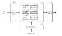
도1은 통상적인 반도체 메모리장치의 블럭구성도이다.1 is a block diagram of a conventional semiconductor memory device.
도1을 참조하여 살펴보면, 통상적인 메모리 장치는 로우어드레스를 입력받아 디코딩하여 출력하는 로우어드레스 입력부(20)와, 컬럼어드레스를 입력받아 디코딩하여 출력하는 컬럼어드레스 입력부(30)와, 다수개의 단위셀로 구성된 셀어레이 (Cell array)(110,120,130,140)를 다수 구비하여 로우어드레스 입력부(20)와 컬럼어드레스 입력부(30)에서 출력되는 신호에 해당되는 데이터를 출력하는 셀영역(100)과, 셀영역(100)에서 출력되는 데이터를 외부로 출력하거나, 외부에서 입력된 데이터를 셀영역으로 전달하기 위한 데이터 입출력부(40)를 구비한다.Referring to FIG. 1, a typical memory device includes a low
셀영역(100)은 셀어레이(110,120,130,140)에서 출력되는 데이터 신호를 증폭하여 데이터 출력부(40)로 출력하기 위한 센스앰프부(150,160)를 구비하고 있다.The
또한, 셀영역의 각 셀어레이(110,120,130,140)는 다수의 단위셀을 구비하고 있다.In addition, each
센스앰프부는 메모리 장치가 리드 동작시에는 전술한 바와 같이 셀어레이에 전달되는 데이터 신호를 감지증폭하여 데이터 입출력부(40)로 출력하고, 메모리 장치가 라이트동작시에는 데이터 입출력부(40)에서 전달된 데이터를 래치하고 셀어레이로 전달하는 역활을 하게 된다.The sense amplifier unit senses and amplifies the data signal transmitted to the cell array during the read operation as described above and outputs the data signal to the data input /
도2은 종래기술에 의해 반도체 메모리 장치를 나타내는 블럭도로서, 특히 셀어레이를 나타내는 블럭구성도이다.Fig. 2 is a block diagram showing a semiconductor memory device according to the prior art, in particular a block diagram showing a cell array.
도2를 참조하여 살펴보면, 반도체 메모리 장치의 셀어레이는 다수의 워드라인(WL0, WL1, WL2, ...)과 다수의 비트라인(BL,/BL)이 교차하면서 구비되면, 교차되는 지점마다 하나의 단위셀이 구비된다.Referring to FIG. 2, when a plurality of word lines WL0, WL1, WL2,... And a plurality of bit lines BL and / BL cross each other, the cell array of the semiconductor memory device may be disposed at each crossing point. One unit cell is provided.
하나의 단위셀(CELL1)은 스위치 역할을 하는 모스트랜지스터(예를 들어 M0)와 캐패시터(예를 들어 C0)로 구성되는데, 단위셀을 구성하는 모스트랜지스터(M0)는 게이트가 워드라인(WL0)과 접속되며, 일측은 비트라인(BL)에 타측은 캐패시터 (C0)에 접속되며, 캐패시터(C0)는 일측이 모스트랜지스터(M0)의 타측 접속되며, 타측으로는 플레이트 전압(PL)을 인가받게 된다.One unit cell CELL1 includes a MOS transistor (for example, M0) and a capacitor (for example, C0) serving as a switch. The MOS transistor (M0) constituting the unit cell has a gate having a word line (WL0). One side is connected to the bit line BL, the other side is connected to the capacitor C0, and the capacitor C0 is connected to the other side of the MOS transistor M0, and the other side to receive the plate voltage PL. do.
이웃한 워드라인(WL0,WL1)에 접속되는 두개의 단위셀(CELL1,CELL2)은 짝을 이루며 하나의 비트라인(BL)에 공통으로 연결되도록 되어 있으며, 두 비트라인은 셀어레이의 일측에 구비되는 센스앰프부(150)의 센스앰프(152a)에 접속되도록 되어 있다.Two unit cells CELL1 and CELL2 connected to neighboring word lines WL0 and WL1 are paired and connected to one bit line BL in common, and two bit lines are provided on one side of the cell array. It is connected to the
만약 단위셀(CELL1)의 데이터를 리드하려면, 워드라인(WL0)이 선택되어 활성화되고, 그로 인해 단위셀(CELL1)의 모스트랜지스터(M0)가 턴온되어 캐패시터(C0)에 저장된 데이터가 비트라인(BL)에 인가된다.If the data of the unit cell CELL1 is to be read, the word line WL0 is selected and activated so that the MOS transistor M0 of the unit cell CELL1 is turned on so that the data stored in the capacitor C0 is stored in the bit line (B0). BL).
비트라인 센스앰프(152a)는 데이터 신호가 인가된 비트라인(BL)과 데이터 신호가 인가되지 않은 비트라인바(/BL)의 전압레벨 차이를 감지하여 증폭하게 된다.The bit
비트라인 센스앰프(152a)의 증폭 동작이 완료된 이후에, 두 비트라인쌍(BL)에 래치된 감지 증폭된 데이터는 외부 데이터라인(LDB)을 통해 외부로 출력된다.After the amplification operation of the bit
이 때 데이터 신호는 비트라인에 있게 되는데, 비트라인바에도 상대적인 데이터를 증폭 및 래치시켜, 셀어레이의 외부로 데이터를 전달할 때에는 쌍으로 데이터를 전달하게 된다.At this time, the data signal is in the bit line, and amplifies and latches the relative data in the bit line bar, so that data is transmitted in pairs when data is transferred to the outside of the cell array.
단위셀(CELL1)의 캐패시터(C0)에 데이터 1(즉 전하가 충전되어 있는 경우)이 저장되어 있다면, 비트라인(BL)은 전원전압 레벨로 증폭되고 비트라인바(/BL)는 접지전압 레벨로 증폭 된다. 또한 단위셀(CELL1)의 캐패시터에 데이터 0(즉 전하가 방전되어 있는 상태)이 저장되어 있다면, 비트라인(BL)은 접지전압 레벨로 증폭되 고, 비트라인바(/BL)는 전원전압레벨로 증폭된다.If data 1 (that is, charge is charged) is stored in the capacitor C0 of the unit cell CELL1, the bit line BL is amplified to the power supply voltage level and the bit line bar / BL is the ground voltage level. Is amplified. In addition, if data 0 (that is, the state where the charge is discharged) is stored in the capacitor of the unit cell CELL1, the bit line BL is amplified to the ground voltage level, and the bit line bar / BL is the power supply voltage level. Is amplified.
이 때 단위셀에 데이터를 나타내기 위해 저장된 전하는 매우 작은 양이기 때문에 비트라인의 전압을 증가시키는데 사용한 후에는 단위셀의 캐패시터에 재충전을 해야한다. 센스앰프에 래치된 데이터 신호를 이용해 단위셀의 캐패시터에 재충전동작이 완료되면, 워드라인이 비활성화된다.At this time, since the charge stored to represent data in the unit cell is a very small amount, the capacitor of the unit cell must be recharged after it is used to increase the voltage of the bit line. When the recharging operation is completed on the capacitor of the unit cell by using the data signal latched in the sense amplifier, the word line is deactivated.
만약 단위셀(CELL3)의 데이터를 리드하는 경우에는 워드라인(WL2)가 선택되어 활성화되어 모스트랜지스터(M2)가 턴온되어 캐패시터(C2)에 저장된 데이터가 비트라인바(/B)L에 인가된다. 센스앰프는 비트라인바(/BL)와 비트라인의 전압레벨 차이를 감지하여 증폭하게 되고, 증폭이 끝난 후에는 외부 데이터라인(LDB)을 통해 외부로 출력된다. 이 때에는 비트라인바(/BL)에 데이터 신호가 인가되면, 그 반대의 신호가 비트라인에 인가되는 것이다.If the data of the unit cell CELL3 is read, the word line WL2 is selected and activated, and the MOS transistor M2 is turned on so that the data stored in the capacitor C2 is applied to the bit line bar L / B. . The sense amplifier senses and amplifies the voltage level difference between the bit line bar (/ BL) and the bit line. After the amplification, the sense amplifier is output to the outside through the external data line (LDB). In this case, when a data signal is applied to the bit line bar / BL, the opposite signal is applied to the bit line.
계속해설 살펴보면, 단위셀에 데이터를 라이트하는 경우에도 전술한 리드동작에서와 같이, 선택된 단위셀에 대응하는 워드라인이 활성화된 이후에 단위셀에 있는 데이터를 감지증폭하게 된다. 이후에 비트라인 센스앰프(152a)에 감지증폭되어 래치된 데이터가 외부에서 전달된 라이트할 데이터로 교체된다.As described above, even when data is written to the unit cell, the data in the unit cell is sensed and amplified after the word line corresponding to the selected unit cell is activated as in the above-described read operation. Thereafter, the sensed amplified and latched data of the bit
교체된 데이터는 비트라인 센스앰프(152a)에 래치되고, 그 래치된 도안 선택된 단위셀의 캐패시터에 저장이 된다. 선택된 단위셀의 캐패시터에 저장이 완료되면, 워드라인이 비활성화된다.The replaced data is latched in the bit
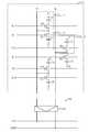
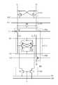
도3은 종래기술에 의해 센스앰프와 셀어레이간의 연결관계를 나타내는 블럭구성도로서, 특히 쉐어드(Shared) 비트라인 센스앰프 구조를 나타내는 블럭구성도 이다.3 is a block diagram showing a connection relationship between a sense amplifier and a cell array according to the prior art, and in particular, a block diagram showing a shared bit line sense amplifier structure.
도3을 참조하여 살펴보면, 셀영역(100)에는 다수의 셀어레이(100,130,180)에는 구비된 단위셀의 데이터를 감지증폭하기 위한 센스앰프를 구비한 센스앰프부(150,170)가 셀어레이의 사이사이에 구비되어 있다.Referring to FIG. 3, in the
센스앱프부(150)에는 다수의 센스앰프가 구비되는데, 하나의 셀어레이에 접속된 비트라인쌍의 갯수에 대응하는 수만큼의 센스앰프가 구비되어야 하는데, 회로의 면적을 줄이기 위해 사용하는 쉐어드 비트라인 센스앰프 구조인 경우에는 두개의 셀어레이당 하나의 센스앰프부를 공휴하기 때문에, 두개의 비트라인 쌍마다 하나의 센스앰프가 구비되면 된다.The
이전에는 셀어레이마다 하나의 센서앰프부가 구비되어 셀어레이중의 한 단위셀의 데이터가 비트라인에 인가되면, 이를 감지, 증폭하였으나, 현재에는 메모리장치의 고집적을 위해서 2개의 셀어레이(110,130)) 당 하나의 센스앰프부(150)를 구비하고, 적절한 연결신호(BISH, BISL)에 따라 센스앰프부와 셀 어레이(110,130)를 연결 또는 분리 시켜고 있다.Previously, one sensor amplifier unit was provided for each cell array, and when data of one unit cell of the cell array was applied to the bit line, the sensor amplifier was sensed and amplified. However, two
예컨대, 제1 연결신호(BISH)에 활성화되면, 제1 연결부(151)가 인에이블되어 센스앰프부(150)과 셀어레이0(110)가 연결되고, 제2 연결신호(BISL)가 활성화되면, 제2 연결부(153)가 인에이블되어 센스앰프부(150)와 셀어레이1(130)가 연결된다.For example, when the first connection signal BISH is activated, the
센스앰프부(150)에는 연결부와 센스앰프외에도 프리차지부와 데이터출력부등이 구비되는데, 도4에 자세하게 도시하였다.The
도4는 도2에 도시된 센스앰프부의 일예를 나타내는 블럭구성도이다.4 is a block diagram illustrating an example of the sense amplifier unit illustrated in FIG. 2.
도4를 참조하여 살펴보면, 센스앰프부(150)는 센스앰프 전원공급단(SAP,SAN)에 입력되는 전압에 의해 동작하여, 비트라인(BL, /BL)의 신호 차이를 증폭하기 위한 센스앰프(152a)와, 센스앰프(152a)가 동작하지 않을 때에 출력되는 프리차지신호(BLEQ)에 인에이블되어 비트라인 프리차지 전압(VBLP)으로 비트라인(BL,/BL)을 프리차지하기 위한 프리차지부(155a)와, 프리차지신호(BLEQ)에 응답하여 셀어레이0(110)에 연결된 두 비트라인(BL,/BL)의 전압레벨을 같게 하기 위한 제1 이퀄라이제이션부(154a)와, 프리차지신호(BLEQ)에 응답하여 셀어레이1(130)에 연결된 비트라인(BL,/BL)의 전압레벨을 같게 하기 위한 제2 이퀄라이제이션부(156a)와, 칼럼어드레스에 의해 생성되는 컬럼제어신호(YI)에 의해 센스앰프(152a)에 의해 증폭된 데이터 신호를 데이터 라인(LDB, LDBB)을 통해 외부로 출력하기 위한 데이터출력부(157a)로 구성된다.Referring to FIG. 4, the
또한, 전술한 바와 같이, 센스앰프부(150)은 센스앰프(155a)를 셀어레이0 또는 셀어레이1과 연결 또는 분리시키기 위한 제1 및 제2 연결부(151a,153a)를 구비한다.In addition, as described above, the
도5는 종래기술에 의해 반도체 메모리 장치의 동작을 나타내는 파형도이다.Fig. 5 is a waveform diagram showing the operation of the semiconductor memory device according to the prior art.
계속해서 도1 내지 도4를 참조하여 종래기술에 의한 반도체 메모리 장치의 센스앰프 동작을 자세히 살펴본다.Subsequently, a sense amplifier operation of the semiconductor memory device according to the related art will be described in detail with reference to FIGS. 1 to 4.
반도체 메모리 장치는 데이터를 리드하는 동작을 프리차지구간(Precharge), 리드명령어구간(Read), 센싱구간(Sense), 재저장구간(Restore)으로 나누어서 동작한다.The semiconductor memory device operates by reading data into a precharge section, a read command section Read, a sensing section Sense, and a restore section.
또한 데이터를 라이트하는 동작도 전술한 리드하는 동작과 전체적인 구성은 같으며, 리드명령어구간 대신에 라이트명령어가 입력된 구간이 있으며, 데이터가 외부로 출력되는 대신에 외부에서 입력된 데이터가 센스앰프에 래치되는 동작이 다를 분이다. 이하에서는 리드에 관한 동작을 자세히 살펴본다.In addition, the operation of writing data has the same general structure as the above-described read operation, and there is a section in which a write command is input instead of a read command section, and the data input from the outside is sent to the sense amplifier instead of being output to the outside. The latching operation is different. Hereinafter, the operation of the read will be described in detail.
또한 이하의 설명에서 캐패시터에 전하가 충전되어 데이터 1이 저장되어 있는 것으로 가정하며, 데이터 리드 동작시 제1 연결부(151a)가 인에이블되고 제2 연결부(153a)는 디스에이블되어 센스앰프부(150)는 셀어레이0(110)에 연결되는 것으로 가정한다.In addition, in the following description, it is assumed that a capacitor is charged and
프리차지 구간(Precharge)동안에는 두 비트라인쌍(BL,/BL)은 프리차지 전압이 인가되어 있는 상태이며 모든 워드라인은 비활성화되어 있는 상태이다. 프리차지 전압은 보편적으로 1/2 코어전압(Vcore/2 =VBLP)을 사용한다.During the precharge period, the two bit line pairs BL and / BL are in a state where a precharge voltage is applied and all word lines are in an inactive state. Precharge voltage is commonly used 1/2 core voltage (Vcore / 2 = VBLP).
이 구간에서는 프리차지신호(BLEQ)가 하이레벨로 인에이블되어 제1 및 제2 이퀄라이제이션부(154a, 157a)와 프리차지부(155a)가 인에이블되어 두 비트라인쌍의 전압레벨은 1/2 코어전압(Vcore)이다. 이 때 제1 및 제2 연결부(151a,153a)는 인에이블되어 있는 상태이다.In this section, the precharge signal BLEQ is enabled at a high level, and the first and
도5의 파형 SN은 단위셀의 캐패시터에 인가되는 전압레벨로서, 데이터 1을 저장하고 있는 경우를 나타냈기 때문에 코어전압(Vcore) 레벨을 나타낸다.The waveform SN in Fig. 5 is a voltage level applied to the capacitor of the unit cell, and represents the core voltage Vcore level since the case where
이어서 리드명령어가 입력되어 실행되는 리드명령어 구간(Read)에서는 제1 연결부(151a)는 인에이블상태를 유지하고 제2 연결부(153a)는 디스에이블 상태가 되어 비트라인 센스앰프부(150)는 일측에 구비되는 셀어레이0(110)와 연결되고, 타 측에 구비되는 셀어레이1(130)과는 분리된다.Subsequently, in the read command section Read in which the read command is input and executed, the
또한, 워드라인(WL)에 고전압에 의해 활성화되어 재저장 구간(Restore)까지 유지된다.In addition, the word line WL is activated by a high voltage and is maintained until a restore period.
이 때 워드라인에는 전원전압보다 높은 고전압(Vpp)이 인가되는데, 이는 반도체 메모리 장치의 전원전압이 낮아지는 반면, 동작속도는 더 고속으로 동작되도록 요구되는 이를 충족시키기 위해서 반도체 메모리 장치의 셀영역에 공급되는 코어전압(Vcore)보다 더 높은 고전압(Vpp)을 생성하여 워드라인(WL)의 활성화에 사용하는 것이다.At this time, a high voltage (Vpp) higher than the power supply voltage is applied to the word line. This means that the power supply voltage of the semiconductor memory device is lowered, but the operating speed is applied to the cell region of the semiconductor memory device in order to satisfy the required operation speed. The high voltage Vpp higher than the supplied core voltage Vcore is used to activate the word line WL.
워드라인(WL)이 활성화되면, 대응하는 단위셀의 모스트랜지스터가 턴온되어 캐패시터에 저장된 데이터가 비트라인(BL)에 인가된다.When the word line WL is activated, the MOS transistor of the corresponding unit cell is turned on, and data stored in the capacitor is applied to the bit line BL.
따라서 1/2 코어전압(Vcore)으로 프리차지되어 있던 비트라인(BL)의 전압이 일정부분 상승하게 되는데, 이 때 캐패시터에 코어전압레벨로 충전되어 있었다 하더라도 비트라인(BL)의 기생캐패시턴스(Cb)에 비해 단위셀의 캐패시터가 가지는 캐패시턴스(Cc)가 매우 작아서 비트라인의 전압을 코어전압까지 상승시키지 못하고, 1/2 코어전압에서 일정전압(ΔV) 만큼만 상승시키게 된다.Therefore, the voltage of the bit line BL, which is precharged to 1/2 core voltage Vcore, rises to a certain degree. At this time, even if the capacitor is charged at the core voltage level, the parasitic capacitance Cb of the bit line BL is Since the capacitance Cc of the unit cell capacitor is very small, the voltage of the bit line cannot be increased to the core voltage, but is increased only by a constant voltage ΔV at the half core voltage.
도5에서 단위셀 캐패시터에 인가되는 전압레벨과 비트라인(BL)에 인가되는 전압레벨이 리드명령어 구간(Read)에서 1/2 코어전압에서 일정전압(ΔV)만큼만 상승한 것을 알 수 있다.In FIG. 5, it can be seen that the voltage level applied to the unit cell capacitor and the voltage level applied to the bit line BL have increased only by a constant voltage ΔV at the half core voltage in the read command period Read.
한편, 비트라인바에는 어떠한 추가적인 전하도 공급되지 않아서 1/2 코어전압(Vcore)을 유지하게 된다.On the other hand, no additional charge is supplied to the bit line bar to maintain the half core voltage (Vcore).
이어서 센싱구간(Sense)에서 비트라인 센스앰프(152a)에 프리차지 구간동안 1/2 코어전압(Vcore)을 유지하던 제1 및 제2 센스앰프 전압공급단(SAP,SAN)이 각각 코어전압과 접지전압으로 공급되고, 그로 인해 비트라인 센스앰프(152a)는 두 비트라인(BL,/BL)의 전압차이를 감지하여 감지 증폭을 하여 두 비트라인(BL,/BL)에서 상대적으로 전압레벨이 높은 쪽은 코어전압(Vcore)으로 증폭하고, 상대적으로 전압레벨이 낮은 쪽은 접지전압으로 증폭한다.Subsequently, the first and second sense amplifier voltage supply stages SAP and SAN, which maintain 1/2 core voltage Vcore during the precharge period in the bit
여기서는 비트라인(BL)이 비트라인바(/BL)보다 높은 전압레벨을 유지하기 때문에 감지증폭이 끝나면 비트라인(BL)은 코어전압(Vcore)으로 비트라인바(/BL)는 접지전압으로 된다.In this case, since the bit line BL maintains a higher voltage level than the bit line bar / BL, the bit line BL becomes the core voltage Vcore and the bit line bar / BL becomes the ground voltage after the sensing amplification is completed. .
이어서 재저장구간(Restore)에서는 리드 구간에서 비트라인의 전압레벨을 1/2 코어전압(Vcore)에서 상승시키기 위해 단위셀의 캐패시터에 저장된 데이터용 전하가 방전되었던 것을 재충전하게 된다. 재충전이 완료나면 워드라인은 다시 비활성화된다.Subsequently, in the restore period, the data charge stored in the capacitor of the unit cell is discharged to increase the voltage level of the bit line at the half core voltage Vcore in the read period. After recharging is complete, the wordline is deactivated again.
이어서 다시 프리차지구간으로 되어 센스앰프로 공급되던 제1 및 제2 센스앰프 전압공급단(SAP,SAN)이 1/2 코어전압으로 유지되고, 프리차지 신호(BLEQ)가 활성화되어 입력되어 제1 및 제2 이퀄라이제이션부(154a,157a)와 프리차지부(155a)가 활성화되며 프리차지 전압(VBLP)이 공급된다. 이 때 제1 및 제2 연결부(151a,153a)에 의해 센스앰프부(150)은 일측과 타측에 구비된 셀어레이0,1(110,130)과 연결된다.Subsequently, the first and second sense amplifier voltage supply stages SAP and SAN, which are supplied to the sense amplifier again after being precharged, are maintained at 1/2 core voltage, and the precharge signal BLEQ is activated and inputted. And the
기술이 점점 더 발달하면서, 메모리 장치를 구동하는 전원전압의 레벨은 점 차 작아져 왔다. 그러나, 전원전압의 크기가 줄어들더라도 메모리 장치의 동작속도는 유지되거나 오히려 더 고속으로 움직이도록 요구받게 된다.As technology develops more and more, the level of the power supply voltage for driving a memory device has gradually decreased. However, even if the magnitude of the power supply voltage is reduced, the operating speed of the memory device is maintained or rather is required to move at a higher speed.
전술한 바와 같이 동작하는 메모리 장치에 전원전압으로 이용하여 전원전압보다는 낮은 레벨의 코어전압(Vcore)과 코어전압(Vcore) 보다는 높은 레벨의 고전압을 내부적으로 생성시켜 적절하게 사용하고 있다.The memory device operating as described above is used as a power supply voltage to internally generate a core voltage Vcore lower than the power supply voltage and a high voltage higher than the core voltage Vcore.
지금까지는 전원전압을 적당히 줄이더라도 별다른 방법을 사용하지 않고, 메모리 장치의 공정기술을 더 줄이는 것만으로도 요구되는 동작속도를 확보할 수 있었다.Until now, even if the power supply voltage was properly reduced, the required operation speed could be secured by further reducing the process technology of the memory device without using a different method.
예를 들면, 3.3V에서 2.5V 또는 더 이하로 전원전압을 줄인다 하더라도 제조공정 기술을 500nm 에서 100nm까지 점차적으로 줄이게 되는 과정에서 요구되는 동작속도를 만족시킬 수 있었던 것이다. 즉, 공정기술을 줄이게 되면, 제조되는 트랜지스터의 소비전력이 이전보다 줄며, 같은 전압을 공급하게 되면 이전보다 고속으로 동작시킬 수 있기 때문이다.For example, even if the power supply voltage was reduced from 3.3V to 2.5V or less, it was possible to meet the required operating speed in the process of gradually reducing the manufacturing process technology from 500nm to 100nm. That is, if the process technology is reduced, the power consumption of the transistor to be manufactured is reduced than before, and if the same voltage is supplied, the transistor can be operated at a higher speed than before.
그러나, 100nm이하에서는 공정기술을 예전과 같이 줄이는 것이 매우 어렵게 된다.However, below 100 nm, it becomes very difficult to reduce the process technology as before.
또한, 요구되는 전원전압은 더 낮아져 2.0V 이하 1.5V 까지 심지어는 1.0V까지 낮아지고 있는 상황에서는 공정기술을 줄이는 것만으로 요구되는 동작속도를 이전과 같이 유지하는 것이 매우 어렵게 되고 있다.In addition, in the situation where the required power supply voltage is lowered and lowered from 2.0V to 1.5V and even to 1.0V, it is very difficult to maintain the required operating speed as before by simply reducing the process technology.
또한, 메모리 장치에 입력되는 전원전압의 레벨이 일정한 레벨이하로 작아지게 되면, 메모리 장치를 이루고 있는 모스트랜지스터의 동작 마진이 매우 작아서 요구되는 동작속도에 맞게 동작되지도 않을 뿐더러, 안정적으로 동작하는 것도 신뢰할 수 없게 되는 것이다.In addition, when the level of the power supply voltage input to the memory device is lowered below a certain level, the operating margin of the MOS transistor constituting the memory device is very small, so that it may not operate at a required operating speed and may also operate stably. It becomes unreliable.
기본적으로 모스트랜지스터의 턴온전압이 일정한 레벨을 유지하는 상황에서는 메모리 장치에 입력되는 구동전압의 레벨이 일정한 레벨이하로 작아지면, 비트라인 센스앰프에서 안정적으로 두 비트라인쌍에 인가된 전압의 차이를 감지하여 증폭하는데 많은 시간이 걸리게 된다.Basically, in a situation where the turn-on voltage of the MOS transistor is maintained at a constant level, when the level of the driving voltage input to the memory device decreases below a certain level, the bit line sense amplifier stably maintains the difference between the voltages applied to the two bit line pairs. It takes a lot of time to detect and amplify.
이 때 약간의 노이즈만 발생하여도(즉 1/2코어전압에서 약간의 노이즈로 인해 비트라인전압레벨이 상승하거나 하강한 경우에) 센스앰프가 감지하지 못하게 되는 경우도 있다.In this case, even if only a little noise occurs (i.e., when the bit line voltage level rises or falls due to a slight noise at 1/2 core voltage), the sense amplifier may not detect.
따라서 메모리 장치의 구동전압을 일정한 레벨이하로 줄이는 것이 현재의 기술로는 매우 어려운 일이다.Therefore, it is very difficult with the current technology to reduce the driving voltage of the memory device below a certain level.
또한, 메모리 장치의 제조기술이 매우 줄어들게 되면, 각 단위셀을 이루는 모스트랜지스터의 게이트 전극과 바로 이웃하여 배치되는 비트라인간의 간격도 매우 작아져, 게이트 전극와 비트라인간에 누설전류가 흐르게 된다. 이 때 흐르는 누설전류를 블리드 전류(Bleed Current)라고 한다.In addition, if the manufacturing technology of the memory device is greatly reduced, the gap between the gate electrodes of the MOS transistors forming each unit cell and the bit lines immediately adjacent to each other becomes very small, and a leakage current flows between the gate electrodes and the bit lines. The leakage current flowing at this time is called bleed current.
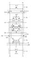
도6은 종래기술에 의한 반도체 메모리 장치의 문제점을 나타내기 위한 단면도로서 특히 저전압 반도체 메모리 장치에서 누설전류의 문제점을 나타내는 단면도이다.6 is a cross-sectional view illustrating a problem of a semiconductor memory device according to the prior art, and particularly, a cross-sectional view illustrating a problem of a leakage current in a low voltage semiconductor memory device.
도6은 반도체 메모리 장치의 한 단위셀의 단면도로서, 기판(10)상에 소자분리막(11)과 소스/드레인 접합영역(12a,12b)와, 게이트 전극(13)과 비트라인(17)과, 캐패시터(14,16,16)과, 절연막(18,19)들이 구비되어 있다.6 is a cross-sectional view of a unit cell of a semiconductor memory device, in which a
반도체 메모리 장치의 공정기술이 줄어들게됨으로서 해서, 게이트 전극(13)과 비트라인(17)의 간격(A)가 점점 더 좁하지게 되어 충분한 절연을 시키기가 매우 어렵게 된다.As the process technology of the semiconductor memory device is reduced, the distance A between the gate electrode 13 and the
이 상태에서 프리차지 구간동안에는 비트라인에 1/2 코어전압이 인가되어 있게 되고, 워드라인이 되는 게이트 전극에는 접지전압이 인가되어 있다.In this state, the half-core voltage is applied to the bit line during the precharge period, and the ground voltage is applied to the gate electrode serving as the word line.
공정상의 에러로 인해 비트라이과 워드라인으로되는 게이트 전극과 단락이 될 수도 있는데, 이 경우에는 비트라인에서 워드라인으로 누설전류인 블리드 전류가 프리차지 동안에 계속 흐르게 되는 것이다.Due to a process error, there may be a short circuit between the gate electrode and the bit line and the word line. In this case, the bleed current leakage current from the bit line to the word line continues to flow during the precharge.
메모리 장치를 제조하고 난 이후에 결함이 있는 에러셀은 여분으로 준비된 예비셀로 대체하게 되는 리페어 공정을 진행하게 되는데, 이 때에 메모리 장치의 특성상 하나의 단위셀로 대체되는 것이 아니라고 워드라인별로 리페어 공정을 진행한다.After manufacturing the memory device, the defective error cell is replaced with a spare cell prepared in advance. In this case, the repair process for each word line is not replaced by one unit cell due to the characteristics of the memory device. Proceed.
따라서 메모리 장치가 동작할 때에는 결함이 발견된 단위셀에 대응하는 워드라인은 사용하지 않고 여분으로 준비된 예비 워드라인을 사용하게 되는 것이다.Therefore, when the memory device operates, the word line corresponding to the unit cell in which the defect is found is used instead of the spare word line.
이 때에 결함이 전술한 워드라인인 게이트 전극과 비트라인간의 단락으로 발생한 것이라면, 예비워드라인으로 대체되어 동작상에는 문제가 없다 하더라도, 여전히 1/2 코어전압으로 프리차지되는 비트라인에서 워드라인으로 블리드 전류가 계속 흐르게 되는 것이다.If the defect is caused by a short circuit between the gate electrode and the bit line, the word line described above, the bleed from the bit line still precharged to 1/2 core voltage to the word line, even if it is replaced with a spare word line and there is no problem in operation. The current continues to flow.
기술이 발달하면서 저전력으로 동작시키는 것을 매우 중요한 문제인데, 전술 한 블리드 전류가 발생하게 되면 동작상으로는 문제가 없다 하더라도 반도체 메모리 장치를 시스템에 사용할 수 없게 되는 것이다.As technology advances, it is very important to operate at low power. When the above-mentioned bleed current occurs, the semiconductor memory device cannot be used in the system even if there is no problem in operation.
블리드 전류를 줄이기 위해 블리드 전류가 흐르는 경로에 저항을 추가적으로 구비하는 아이디어도 있으나, 블리드 전류를 일정부분 감소시키는 역할만 할 뿐 근본적인 해결책은 되지 못한다.Some ideas include additional resistance in the path through which the bleed current flows to reduce the bleed current, but it only serves to reduce the bleed current to some extent and is not a fundamental solution.
한편, 프리차지시에 비트라인의 전압을 접지전압으로 유지하게 되면, 사용하지 않는 워드라인과 비트라인의 전압레벨이 같게 되어 전술한 블리드 전류의 발생을 방지할 수 있다.On the other hand, if the voltage of the bit line is maintained at the ground voltage during precharging, the voltage levels of the unused word line and the bit line are the same, thereby preventing generation of the above-described bleed current.
그러나, 접지전압으로 프리차지를 하게 되면, 데이터를 리드하거나 라이트하고 난 이후에 프리차지 구간으로 진입할 때에 비트라인쌍(BL,/BL의 한쪽은 전원전압 나머지 한쪽은 접지전압을 유지하게 된다.)의 한쪽 라인을 접지전압으로 강제로 강하시키는 과정에서 불필요한 전력이 소모된다.However, when the precharge is performed with the ground voltage, one of the bit line pairs BL and / BL maintains the ground voltage while one of the bit line pairs BL and / BL enters the precharge period after the data is read or written. Unnecessary power is consumed in the process of forcibly dropping one of the lines to ground voltage.
가장 널리 사용하는 방법인 1/2 전원전압을 비트라인의 프리차지 전압으로 사용하게 되면, 프리차지 구간으로 진입할 때에 한 비트라인쌍의 전압레벨을 등가화시키고, 이후에는 1/2전원전압을 공급하면된다.When the 1/2 supply voltage, the most widely used method, is used as the precharge voltage of the bit line, the voltage level of one bit line pair is equalized when entering the precharge section, and then the 1/2 supply voltage is applied. Supply it.
따라서 프리차지 전압으로 만들어 주는 과정에서 별도의 전력이 소비되지는 않기 때문에 접지전압으로 프리차지 하는 경우보다 전력소비는 적다.Therefore, since no extra power is consumed in the process of making the precharge voltage, power consumption is less than that of the precharge with ground voltage.
그러나, 프리차지 전압으로 1/2 전원전압을 유지하게 되면, 전술한 바와 같이 워드라인과 비트라인간의 전압차이로 인해 반도체 메모리 장치가 동작중에 계속해서 블리드 전류가 발생하기 때문에 저전력 반도체 메모리 장치에는 적용하기가 매우 어렵다.However, if the 1/2 supply voltage is maintained at the precharge voltage, the bleed current is continuously generated while the semiconductor memory device is operating due to the voltage difference between the word line and the bit line as described above. Very difficult to do
본 발명은 전술한 문제점을 해결하기 위해 제안된 것으로, 블리드 전류의 발생을 방지하면서도, 프리차지동작시 소비전력을 최소화할 수 있는 반도체 메모리 장치를 제공함을 목적으로 한다.The present invention has been proposed to solve the above problems, and an object thereof is to provide a semiconductor memory device capable of minimizing power consumption during a precharge operation while preventing generation of a bleed current.
또한, 본 발명은 입력되는 전원전압이 낮은 상태에서도 고속으로 동작할 수 있는 반도체 메모리 장치를 제공함을 목적으로 한다.
In addition, an object of the present invention is to provide a semiconductor memory device capable of operating at a high speed even in a state in which the input power supply voltage is low.
본 발명은 전원전압과 접지전압을 인가받아 동작하는 반도체 메모리 장치에 있어서, 제1 비트라인에 데이터 신호를 전달하기 위한 제1 셀어레이; 제2 비트라인에 데이터 신호를 전달하기 위한 제2 셀어레이; 상기 제1 비트라인 또는 상기 제2 비트라인에 데이터 신호가 인가되면, 제1 비트라인과 제2 비트라인에 인가된 신호의 차이를 감지 및 증폭하는 비트라인 센스앰프; 데이터 신호가 상기 제1 비트라인에 인가될 때에 기준신호를 상기 제2 비트라인에 인가하거나, 데이터 신호가 상기 제2 비트라인에 인가될 때에 상기 기준신호를 상기 제1 비트라인에 인가하기 위한 레퍼런스셀 블럭; 및 프리차지 구간에 상기 제1 비트라인과 상기 제2 비트라인의 전압레벨을 등가화시키기 위한 프리차지부를 구비하며, 프리차지 구간에 상기 제1 비트라인과 제2 비트라인에 프리차지 전압을 별도로 인가하지 않아 플로팅시키는 반도체 메모리 장치를 제공한다.According to an aspect of the present invention, there is provided a semiconductor memory device which operates by receiving a power supply voltage and a ground voltage, comprising: a first cell array configured to transfer a data signal to a first bit line; A second cell array for transferring a data signal to a second bit line; A bit line sense amplifier configured to sense and amplify a difference between a signal applied to the first bit line and the second bit line when a data signal is applied to the first bit line or the second bit line; Reference for applying a reference signal to the second bit line when a data signal is applied to the first bit line, or applying a reference signal to the first bit line when a data signal is applied to the second bit line. Cell block; And a precharge unit configured to equalize voltage levels of the first bit line and the second bit line in a precharge period, and separately precharge voltages of the first bit line and the second bit line in a precharge period. Provided is a semiconductor memory device which is floated without being applied.
또한 본 발명은 오픈 비트라인 구조를 가지며, 전원전압과 접지전압을 인가받아 동작하는 반도체 메모리 장치의 구동방법에 있어서, 상기 제1 비트라인에 데이터 신호를 인가하는 데이터 전달 단계; 상기 제2 비트라인에 기준신호를 인가하는 기준신호 전달 단계; 상기 제1 비트라인과 상기 제2 비트라인의 신호 차이를 감지하고 증폭하여 래치하는 센싱 단계; 및 상기 제1 비트라인과 상기 제2 비트라인의 전압레벨을 등가화시키고 플로팅시키는 프리차지 단계를 포함하는 반도체 메모리 장치의 구동방법을 제공한다.The present invention also provides a method of driving a semiconductor memory device which has an open bit line structure and operates by receiving a power supply voltage and a ground voltage, comprising: a data transfer step of applying a data signal to the first bit line; A reference signal transfer step of applying a reference signal to the second bit line; A sensing step of sensing, amplifying and latching a signal difference between the first bit line and the second bit line; And a precharge step of equalizing and plotting voltage levels of the first bit line and the second bit line.
이하, 본 발명이 속하는 기술분야에서 통상의 지식을 가진 자가 본 발명의 기술적 사상을 용이하게 실시 할 수 있을 정도로 상세히 설명하기 위하여, 본 발명의 가장 바람직한 실시예를 첨부된 도면을 참조하여 설명하기로 한다.Hereinafter, the most preferred embodiments of the present invention will be described with reference to the accompanying drawings so that those skilled in the art can easily implement the technical idea of the present invention. do.
도7은 본 발명의 바람직한 실시예에 따른 반도체 메모리 장치를 나타내는 블럭구성도이다.7 is a block diagram illustrating a semiconductor memory device in accordance with a preferred embodiment of the present invention.
도7을 참조하여 살펴보면, 본 실시예에 따른 반도체 메모리 장치는 각각 하나의 모스트랜지스터와 캐패시터로 각각 이루어진 다수의 단위셀을 구비하는 셀어레이(300a, 300b)와, 셀어레이(300a, 300b)에 접속된 비트라인에 인가되는 데이터 신호를 감지 증폭하기 위한 비트라인 센스앰프를 구비하는 센스앰프부(200a, 200b, 200c)와, 센스앰프부(200a, 200b, 200c)로 기준신호를 제공하기 위한 레퍼런스셀 블럭(400a, 400b, 400c, 400d)과, 프리차지 구간동안에 셀어레이(300a, 300b)에 구비되는 모든 비트라인의 전압레벨을 등가화시키기 위한 제1 및 제2 프리차지용 플로팅 연결부(500a, 500b)를 구비한다.Referring to FIG. 7, a semiconductor memory device according to the present exemplary embodiment may include cell arrays 300a and 300b and cell arrays 300a and 300b each having a plurality of unit cells each including one MOS transistor and a capacitor. For providing a reference signal to the
또한, 제1 프리차지용 플로팅 연결부(500a)는 제1 셀어레이(300a)에 구비된 모든 비트라인과 교차하면서 지나가는 제1 배선(FLOAT)과, 제1 셀어레이(300a)에 구비되는 모든 비트라인에 각각 대응하며, 일측은 제1 배선(FLOAT)에 접속되고, 타측은 대응하는 비트라인에 접속되며, 프리차지 구간동안 활성화된 신호(BLEQ)에 응답하여 턴온되는 다수의 스위치용 모스트랜지스터(TF1,TF2,..)를 구비한다.In addition, the first precharge floating
제1 프리차지용 플로팅 연결부(500a)는 모든 비트라인에 연결된 제1 배선(FLOAT)을 통해, 제1 셀어레이(300a)에 구비된 모든 비트라인의 전압레벨을 프리차지구간동안 같게 만들어 주기 위한 것이다.The first precharge floating
본 실시예에 따른 메모리 장치의 가장 큰 특징은 각 비트라인에 프리차지 구간동안 전압을 제공하지 않는 것이다. 따라서 한 셀어레이에 구비된 각 비트라인의 전압레벨은 서로 다른 상태로 플로팅된 상태를 유지하다가 데이터를 리드 또는 라이트하기 또는 리프레쉬동작이 수행될 때에 셀어레이게 저장된 데이터가 인가된다.The biggest feature of the memory device according to the present embodiment is that no voltage is provided to each bit line during the precharge period. Therefore, while the voltage level of each bit line included in one cell array remains in a different state, data stored in the cell array is applied when data is read or written or a refresh operation is performed.
그러므로 한 셀어레이에 구비된 모든 비트라인의 전압을 같게 유지시켜 주지않아도 상관이 없기 때문에 반드시 플로팅 연결부가 필요한 것은 아니다. 플로팅 연결부가 없게 되면, 한 셀어레이에 구비되는 모든 비트라인의 전압이 프리차지구간에서 서로 다른 전압레벨 상태로 되며, 이 경우에는 각각의 비트라인이 다른 전압레벨을 가진 상태에서 데이터 리드/라이트 또는 리프레쉬 동작을 진행하게 되는 것이다.Therefore, it is not necessary to keep the floating connection because it does not matter even if the voltages of all the bit lines provided in one cell array are kept the same. If there is no floating connection, the voltages of all the bit lines included in one cell array are at different voltage levels in the precharge section, in which case each bit line has a different voltage level. The refresh operation will proceed.
여기서 제2 셀어레이(300b)에 연결된 제2 프리차지용 플로팅 연결부(500b) 역시 전술한 제1 프리차지용 플로팅 연결부(500a)와 같은 방식으로 구성된다.Here, the second precharge floating
도8은 도7에 도시된 레퍼런스셀 블럭의 내부를 나타내는 회로도이다.FIG. 8 is a circuit diagram illustrating an interior of a reference cell block shown in FIG. 7.
도8을 참조하여 살펴보면, 제1 레퍼런스 셀 블럭(400a)은 일측으로 기준신호용 전원공급단(VCP)이 접속된 레퍼런스용 캐패시터(RC1)와, 데이터 신호가 비트라인바(/BLn)에 인가될 때에, 레퍼런스용 캐패시터(RC1)의 타측을 비트라인(BLn)에 연결하기 위한 스위치용 모스트랜지스터(RT1)와, 프리차지 구간 동안에 레퍼런스용 캐패시터(RC1)의 타측에 기준신호용 전원공급단(VCP)을 접속시키기 위한 스위치용 모스트랜지스터(RT1)를 구비한다.Referring to FIG. 8, the first
레퍼런스용 캐패시터(RC)의 캐패시턴스는 제1 셀어레이(300a)에 구비되는 단위셀 캐패시터(Cap)가 가지는 캐패시턴스와 실질적으로 같게 한다.The capacitance of the reference capacitor RC is substantially equal to the capacitance of the unit cell capacitor Cap included in the first cell array 300a.
기준신호용 전원공급단(VCP)에서 공급되는 전압레벨은 접지전압, 전원전압의 1/2, 전원전압중 선택된 하나인 것을 특징으로 하며, 기준신호용 전원공급단(VCP)에 인가되는 전압과 같은 레벨의 전압을 단위셀 캐패시터의 플레이트 전압(PL)으로 공급한다.The voltage level supplied from the power supply terminal (VCP) for the reference signal is selected from the ground voltage, 1/2 of the power supply voltage, and the power supply voltage. The same level as the voltage applied to the power supply terminal (VCP) for the reference signal. Is supplied to the plate voltage PL of the unit cell capacitor.
제1 레퍼런스셀 블럭(400a)에 구비되는 레퍼런스용 캐패시터(RC)의 수는 제1 셀어레이(300a)에 구비되는 비트라인의 수에 대응하여 구비되는데, 만약 제1 셀어레이에 1024개의 비트라인이 구비된다면, 1024개의 비트라인에 각각 대응하는 1024개의 레퍼런스용 캐패시터를 구비하게 된다.The number of reference capacitors RC included in the first
제2 레퍼런스셀 블럭(400c)은 데이터 신호가 비트라인(BLn)에 인가될 때에 기준신호를 비트라인바(/BLn)에 인가하게 된다.The second reference cell block 400c applies a reference signal to the bit line bar / BLn when the data signal is applied to the bit line BLn.
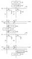
도9는 도7에 도시된 반도체 메모리 장치를 보다 자세히 나타내는 블럭구성도로서, 특히 도7에 도시된 센스앰프부(200a)를 자세히 나타내는 회로도이다.FIG. 9 is a block diagram illustrating the semiconductor memory device shown in FIG. 7 in more detail. In particular, FIG. 7 is a circuit diagram showing in detail the sense amplifier unit 200a shown in FIG.
도9를 참조하여 살펴보면, 센스앰프부는 비트라인(BL) 또는 비트라인바(/BL)에 데이터 신호가 인가되면, 비트라인(BL)과 비트라인바(/BL)에 인가된 신호의 차이를 감지 및 증폭하는 비트라인 센스앰프(210)와, 프리차지 구간에 비트라인(BL)과 비트라인바(/BL)의 전압레벨을 등가화시키기 위한 프리차지부(220)를 구비한다.Referring to FIG. 9, when a data signal is applied to the bit line BL or the bit line bar / BL, the sense amplifier unit may determine a difference between the signal applied to the bit line BL and the bit line bar / BL. A bit
프리차지부(220)는 별도의 프리차치용 전압을 공급받지 않고, 두 비트라인(BL,/BL)의 전압레벨을 같게 하는 역할만을 하게 된다. 따라서 프리차지 구간동안 두 비트라인(BL,/BL)은 플로팅상태를 유지하게 된다.The
프리차지 구간에 비트라인(BL)과 비트라인바(/BL)에 프리차지 전압을 별도로 인가하지 않아 플로팅시키게 된다.The precharge voltage is not applied to the bit line BL and the bit line bar / BL separately in the precharge period, thereby floating.
여기서 비트라인 센스앰프(210)는 접지전압보다 낮은 레벨의 저전압(VBB)과,전원전압보다 높은 레벨의 고전압(VPP)을 이용하여 감지 및 증폭동작을 수행하게 된다. 이 때 저전압(VBB)은 센스앰프 전원공급단(SAN)을 통해 전달되며, 고전압(VPP)는 센스앰프 전원공급단(SAP)을 통해 전달된다.The bit
또한, 본 실시예에 따른 반도체 메모리 장치의 센스앰프부는 제1 셀어레이(300a)에 구비된 비트라인(BL)과 비트라인 센스앰프(210)의 사이에 구비되어, 비트라인 센스앰프(210)를 구동시키기 위한 저전압(VBB)이 비트라인(BL)으로 전달되는 것을 방지하기 위한 제1 전압 클램핑부(250a)와, 제2 셀어레이(300b)에 구비된 비트라인바(/BL)와 비트라인 센스앰프(210)의 사이에 구비되어, 비트라인 센스앰프(210)를 구동시키기 위한 저전압(VBB)이 비트라인바(/BL)로 전달되는 것을 방지하기 위한 제2 전압 클램핑부(250b)를 더 구비한다.In addition, the sense amplifier unit of the semiconductor memory device according to the present exemplary embodiment is provided between the bit line BL and the bit
또한, 본 실시예에 따른 반도체 메모리 장치의 센스앰프부는 제1 셀어레이(300a)와 제1 전압 클램핑부(250a) 사이에 구비된 비트라인(BL)과, 제2 셀어레이(300b)와 제2 전압 클램핑부(250b) 사이에 구비된 비트라인바(/BL)의 전압중 낮은 레벨의 라인전압을 접지전압 레벨로 증폭 및 유지시키기 위한 보조 비트라인 센스앰프(230)를 구비한다.In addition, the sense amplifier unit of the semiconductor memory device according to the present exemplary embodiment may include a bit line BL provided between the first cell array 300a and the first
프리차지부(220)는 비트라인(BL)과 비트라인바(/BL)에 일측과 타측이 각각 접속되며, 게이트로 프리차지구간동안 활성화되어 입력되는 프리차지 신호(BLEQ)를 입력받는 프리차지용 모스트랜지스터(TP1)를 구비한다.The
또한 비트라인 센스앰프(210)는 게이트는 비트라인(SA_/BL)에 접속되며 제1 센스앰프 전원공급단(SAP)에 일측으로 접속되고 타측으로는 비트라인(SA_BL)이 접속된 제1 피모스트랜지스터(TS1)와, 게이트는 비트라인(SA_BL)에 접속되며 제1 센스앰프 전원공급단(SAP)에 일측으로 접속되고 타측으로는 비트라인(SA_/BL)에 접속된 제2 피모스트랜지스터(TS2)와, 게이트는 비트라인(SA_/BL)에 접속되며 제2 센스앰프 전원공급단(SAN)에 일측으로 접속되고 타측으로는 비트라인(SA_BL)이 접속된 제1 엔모스트랜지스터(TS3)와, 게이트는 비트라인(BL)에 접속되며 제2 센스앰프 전원공급단(SAN)에 일측으로 접속되고 타측으로는 비트라인(SA_/BL)가 접속된 제2 엔모스트랜지스터(TS4)를 구비한다.In addition, the bit
제1 전압 클램핑부(250a)는 활성화시에 저전압 레벨을 유지하는 입력신호(BIS)를 게이트로 입력받고, 일측은 비트라인(BL)과 접속되며, 타측은 제1 피모스트랜지스터 및 제1 엔모스트랜지스터(TS1,TS3)의 공통 타측에 접속된 제1 클램핑용 피모스트랜지스터(TBH1)를 구비한다.The first
제2 전압 클램핑부(250b)는 활성화시에 저전압 레벨을 유지하는 입력신호(BIS)를 게이트로 입력받고, 일측은 비트라인바(/BL)와 접속되며, 타측은 제2 피모스트랜지스터 및 제2 엔모스트랜지스터(TS2,TS4)의 공통 타측에 접속된 제2 클램핑용 피모스트랜지스터(TBH2)를 구비한다.The second
보조 비트라인 센스앰프(230)는 일측으로 비트라인 센스앰프(210)이 활성화되는 구간동안 접지전압으로 활성화되어 입력되는 신호(BLPD)를 입력받고, 타측이 제1 셀어레이(300a)와 제1 전압 클램핑부(250a) 사이에 구비된 비트라인(BL)에 접속되고, 게이트가 제2 셀어레이(300b)와 제2 전압 클램핑부(250b) 사이에 구비된 비트라인바(/BL)에 접속된 제1 보조앰프용 모스트랜지스터(TSB1)와, 일측으로 비트라인 센스앰프(210)이 활성화되는 구간동안 접지전압으로 활성화되어 입력되는 신호(BLPD)를 입력받고, 타측이 제2 셀어레이(300b)와 제2 전압 클램핑부(230b) 사이에 구비된 비트라인바(/BL)에 접속되고, 게이트가 제1 셀어레이(300a)와 제1 전압 클램핑부(230a) 사이에 구비된 비트라인(BL)에 접속된 제2 보조앰프용 모스트랜지스터(TSB2)를 구비한다.The auxiliary bit
또한, 본 실시예에 따른 반도체 메모리 장치의 센스앰프부는 비트라인 센스 앰프(210)에 의해 감지증폭된 데이터를 데이터 라인(LDB,LDBB)을 통해 외부로 전달하거나, 데이터 라인(LDB,LDBB)을 통해 외부에서 전달된 데이터를 비트라인 센스앰프(210)로 전달하기 위한 데이터입출력부(240)를 더 구비한다.In addition, the sense amplifier unit of the semiconductor memory device according to the present embodiment transfers the data sensed and amplified by the bit
데이터입출력부(240)는 게이트로 입출력제어신호(YI)를 입력받으며, 일측은 비트라인(SA_BL)에 접속되며 타측은 제1 데이터라인(LDB)에 접속되는 제1 입출력용 모스트랜지스터(TO1)와, 게이트로 입출력제어신호(YI)를 입력받으며, 일측은 비트라인(SA_/BL)에 접속되며 타측은 제2 데이터라인(LDBB)에 접속되는 제2 입출력용 모스트랜지스터(TO2)를 구비한다.The data input /
도10과 도11은 도8에 도시된 반도체 메모리 장치의 동작을 나타내는 파형도이다.10 and 11 are waveform diagrams illustrating an operation of the semiconductor memory device shown in FIG. 8.
이하에서 도7 내지 도11을 참조하여 본 실시예에 따른 반도체 메모리 장치의 동작을 살펴본다.Hereinafter, operations of the semiconductor memory device according to the present embodiment will be described with reference to FIGS. 7 through 11.
본 실시예에 따른 반도체 메모리 장치는 프리차지 구간에 비트라인(BL)과 비트라인바(/BL)에 프리차지 전압을 별도로 인가하지 않아 플로팅시키는 것이 가장 큰 특징이다.In the semiconductor memory device according to the present embodiment, the precharging voltage is not applied to the bit line BL and the bit line bar / BL separately during the precharge period.
또한, 본 실시예에 따른 반도체 메모리 장치는 프리차지 전압으로 접지전압을 사용하며, 비트라인 센스앰프가 접지전압(GND)과 전원전압(VDD)를 사용하여 감지 증폭 동작을 수행하는 것이 아니라, 접지전압(GND)보다 낮은 레벨의 저전압(VBB)와, 전원전압(VDD)보다 높은 레벨의 고전압(VPP)를 사용하여 두 비트라인(BL,/BL)에 인가된 전압차이를 감지하고 증폭하는 것을 특징으로 하고 있다.In addition, the semiconductor memory device according to the present embodiment uses the ground voltage as the precharge voltage, and the bit line sense amplifier does not perform the sense amplification operation using the ground voltage GND and the power supply voltage VDD, but the ground. Detecting and amplifying the voltage difference applied to the two bit lines BL and BL using a low voltage VBB at a level lower than the voltage GND and a high voltage VPP at a level higher than the power supply voltage VDD. It features.
먼저 데이터 '1'을 리드하는 경우를 살펴본다. 이 때 데이터 신호는 비트라인(BL)에 의해 인가되는 것으로 가정한다.First, the case of reading data '1' will be described. In this case, it is assumed that the data signal is applied by the bit line BL.
프리차지 구간(Precharge)부터 살펴보면, 프리차지 구간(Precharge)동안 프리차지 신호(BLEQ)가 하이레벨로 인에이블된 상태를 유지하여 제1 셀어레이(300a)의 비트라인(BL) 및 비트라인바(/BL)의 전압레벨은 등가화된다.Looking at the precharge section Precharge, the bit line BL and the bit line bar of the first cell array 300a may be maintained while the precharge signal BLEQ is enabled at a high level during the precharge section. The voltage level of (/ BL) is equivalent.
본 실시예에 따른 반도체 메모리 장치는 프리차지구간에서 별도의 전압을 두지 않기 때문에 비트라인쌍(BL,/BL, SA_BL,SA_/BL)은 플로팅상태를 유지한다.(t0)Since the semiconductor memory device according to the present embodiment does not have a separate voltage in the precharge section, the bit line pairs BL, / BL, SA_BL, SA_ / BL maintain the floating state. (T0)
따라서 데이터를 리드하거나 라이트하고 난 직후에는 비트라인쌍(BL,/BL)의 전압레벨을 같게 하여 주면, 1/2 전원전압레벨을 유지하게 되지만(비트라인 센스앰프에 의해 감지증폭된 이후에는 비트라인쌍중 하나의 전압레벨은 전원전압이고, 나머지 하나는 접지전압을 유지하게 됨), 별도의 프리차지용 전압을 공급하기 않기 때문에, 일정한 시간이 흐르게 되면, 누설절류로 인해 1/2 전원전압 레벨을 유지하던 비트라인의 전압레벨이 점차적으로 감소하게 된다.Therefore, immediately after reading or writing data, if the voltage level of the bit line pair BL and / BL is the same, 1/2 power supply voltage level is maintained (but after the bit is sensed and amplified by the bit line sense amplifier) The voltage level of one of the line pairs is the power supply voltage, and the other one maintains the ground voltage), and since it does not supply a separate precharge voltage, if a certain time passes, the half power supply voltage is caused by leakage current. The voltage level of the bit line maintaining the level gradually decreases.
계속해서 데이터를 리드 하거나 라이트 하지 않고 프리차지 구간만이 계속된다면 결국 프리차지 구간동안 비트라인(BL,/BL, SA_BL,SA_/BL)의 전압은 접지전압까지 감소하게 된다.If only the precharge period continues without reading or writing data continuously, the voltage of the bit lines BL, / BL, SA_BL, SA_ / BL decreases to the ground voltage during the precharge period.
따라서 프리차지 구간의 길이에 따라 비트라인의 프리차지 전압레벨은 1/2 전원전압에서 접지전압 사이의 변동된 값을 가질 수 있다. 그러므로 프리차지 구간의 어느 시점에서 리드명령어를 수행하느냐에 따라서 플로팅된 비트라인(BL,/BL, SA_BL,SA_/BL)의 전압레벨이 달라지게 되는 것이다.Therefore, the precharge voltage level of the bit line may vary between the 1/2 supply voltage and the ground voltage according to the length of the precharge period. Therefore, the voltage levels of the floated bit lines BL, / BL, SA_BL, and SA_ / BL vary according to which point in the precharge period the read command is executed.
한편, 시간에 따라 비트라인의 프리차지 전압이 변함에 따라 프리차지 구간 내내 셀어레이(300a,300b)에 구비되는 모든 비트라인의 전압레벨을 같게 해주기 위해 제1 및 제2 프리차자용 플로팅 연결부(500a,500b)가 구비된다.Meanwhile, as the precharge voltage of the bit line changes with time, the floating connection unit for the first and second prechargers may be equalized so that the voltage levels of all the bit lines provided in the cell arrays 300a and 300b are the same throughout the precharge period. 500a, 500b) are provided.
프리차지 구간동안 활성화되어 입력되는 프리차지 신호(BLEQ)에 의해 턴온되는 모스트랜지스터(TF1,TF2)와, 프리차지용 플로팅 연결부(500a)에 구비된 배선(FLOAT)에 의해 프리차지 구간내내 각 비트라인의 전압레벨이 변동되더라도 셀어레이에 구비된 모든 비트라인의 플로팅 전압레벨은 같은 값을 가질 수 있게 된다.Each bit throughout the precharge period by the MOS transistors TF1 and TF2 turned on by the precharge signal BLEQ activated and input during the precharge period and the wiring FLOAT provided in the precharge floating
프리차지 구간(Precharge)이 끝나고 리드명령어 구간(Read)이 되어 데이터를 리드하기 위해서 단위셀의 있는 데이터를 비트라인(BL)에 인가하게 되면, 그 이전까지 플로팅되어 조금씩 감소하여 접지전압에서 1/2전원전압 사이의 어떤 레벨에서 인가되는 데이터 신호만큼 비트라인의 전압레벨이 상승한다.(t1)When the precharge period is over and the data in the unit cell is applied to the bit line BL in order to read data after the precharge period is read, the data is plotted until it is decreased until the precharge period is read. The voltage level of the bit line rises by the data signal applied at a level between two power supply voltages (t1).
한편, 비트라인바(/BL)에는 기준신호가 공급되는데, 도8에 도시된 레퍼런스신호(/RWL)이 하이레벨로 되어 모스트랜지스터(RT2)가 턴온되어 레퍼런스용 캐패시터(RC)에 저장되어 있던 기준신호는 비트라인바(/BL)에 인가되어 비트라인바(/BL)의 전압레벨을 일정레벨로 상승시킨다.On the other hand, a reference signal is supplied to the bit line bar / BL, and the reference signal / RWL shown in FIG. 8 is at a high level so that the MOS transistor RT2 is turned on and stored in the reference capacitor RC. The reference signal is applied to the bit line bar / BL to raise the voltage level of the bit line bar / BL to a constant level.
이 때에도 비트라인(/BL,SA_/BL)은 플로팅된 상태의 1/2 전원전압에서 점차적으로 감소하여 어떤 레벨로 되어 있는 상태에서, 인가되는 기준신호만큼 전압레벨이 상승하게 된다.At this time, the bit lines / BL and SA_ / BL are gradually reduced in the 1/2 power supply voltage in the floating state, and the voltage level is increased by the applied reference signal in a state where the bit lines / BL and SA_ / BL are at a certain level.
전술한 바와 같이 레퍼런스용 캐패시터(RC)는 단위셀을 이루는 캐패시터(Cap)와 캐패시턴스를 같게 형성하고, 저장되는 전하량은 데이터가 1일 때 캐패시 터(Cap)에 저장되는 양의 1/2로 한다. 도8의 레퍼런스 캐패시터의 일측단인 기준신호의 출력단(RSN)은 프리차지 구간동안 1/2 전원전압 레벨을 유지하게 된다.As described above, the reference capacitor RC has the same capacitance as the capacitor Cap constituting the unit cell, and the amount of charge stored is 1/2 of the amount stored in the capacitor Cap when the data is 1. do. The output terminal RSN of the reference signal, which is one end of the reference capacitor of FIG. 8, maintains the 1/2 power supply voltage level during the precharge period.
프리차지 구간동안 레퍼런스 캐패시터의 타측단에 인가되는 기준신호 전원공급단(RPL)은 단위셀 캐패시터(Cap)의 플레이트 전압(PL) 레벨과 같은 레벨의 전압이 공급된다. 이 때 공급할 수 있는 전압레벨의 예로서는 전원전압(VDD), 1/2 전원전압(VDD), 접지전압(GND)가 있다.The reference signal power supply terminal RPL applied to the other end of the reference capacitor during the precharge period is supplied with a voltage having the same level as the plate voltage PL of the unit cell capacitor Cap. Examples of voltage levels that can be supplied at this time include power supply voltage VDD, 1/2 power supply voltage VDD, and ground voltage GND.
이렇게 플레이트 전압(PL)과 같은 레벨의 전압을 기준신호 전원 공급단(VCP)에 공급하는 것은 데이터 신호와 비례하여 정확하게 1/2 정도의 신호를 기준신호로 공급하기 위한 것이다.The supply of a voltage at the same level as the plate voltage PL to the reference signal power supply terminal VCP is for supplying a signal of about 1/2 as a reference signal in proportion to the data signal.
따라서 기준신호에 의해 상승되는 비트라인(/BL)의 전압레벨은 데이터 신호에 의해 상승되는 비트라인(BL)의 전압레벨의 1/2이 된다.Therefore, the voltage level of the bit line / BL raised by the reference signal is 1/2 of the voltage level of the bit line BL raised by the data signal.
예를 들어 전원전압이 1.0V이고 데이터 신호에 의해 약 0.2V가 증가되는 경우를 살펴보면, 프리차지 구간의 초기에는 비트라인(BL,/BL)의 전압레벨이 0.5V를 유지하고 있게 된다.For example, when the power supply voltage is 1.0V and the voltage is increased by about 0.2V by the data signal, the voltage level of the bit lines BL and / BL is maintained at 0.5V at the beginning of the precharge period.
이후 프리차지 구간이 계속됨에 따라 비트라인의 전압이 점차 떨어져 약 0.3V 정도로 되었을 때에 데이터 리드동작이 수행되면, 데이터 신호가 인가되는 비트라인(BL)은 0.5V(0.3+0.2V)가 되고, 데이터 신호의 1/2에 해당되는 전하량을 가지는 기준신호가 인가되는 비트라인바(/BL)은 0.4V(0.3V+0.1V)가 되는 것이다.Since the data read operation is performed when the voltage of the bit line gradually drops to about 0.3V as the precharge period continues, the bit line BL to which the data signal is applied becomes 0.5V (0.3 + 0.2V), The bit line bar / BL to which the reference signal having a charge amount corresponding to 1/2 of the data signal is applied is 0.4V (0.3V + 0.1V).
이 때 프리차지 신호(BLEQ)는 프리차지 구간동안에 하이레벨로 활성화되며, 리드 명령어 구간(Read), 센싱구간(Sense) 및 재저장 구간(Restore)동안에는 로우 레벨로 비활성화상태를 유지한다.At this time, the precharge signal BLEQ is activated at a high level during the precharge period, and remains inactive at a low level during the read command period Read, the sensing period Sense, and the restore period.
이어서 센싱구간(Sense)에서 비트라인 센스앰프(210)의 제1 센스앰프 전원공급단(SAP)에는 고전압(VPP)이 공급되고, 제2 센스앰프 전원공급단(SAN)에는 저전압(VBB)이 공급된다.Subsequently, a high voltage VPP is supplied to the first sense amplifier power supply terminal SAP of the bit
따라서 비트라인 센스앰프(210)는 두 비트라인(BL,/BL)에 인가된 전압차이를 감지하여 상대적으로 큰 전압을 가지는 비트라인(BL)을 고전압(VPP) 레벨까지 상승시키고, 비트라인바(/BL)는 접지전압(GND)까지 증폭시킨 후 래치한다.(t2)Accordingly, the bit
비트라인 센스앰프(210)은 전원전압(VDD)과 접지전압(GND)이 아니라 고전압(VPP)과 저전압(VBB)을 이용하여 증폭동작을 하기 때문에 종래보다 고속으로 증폭동작을 수행할 수 있게 된다.Since the bit
이 때 비트라인 센스앰프(210)와 제2 전압 클램핑부(250b)사이에 연결된 비트라인(SA_/BL)은 음의 저전압(VBB)까지 증폭이 되나, 제1 전압 클램핑 연결부(250a)에 의해서 제1 셀어레이(300a)에서 제1 전압 클램핑 연결부(250a)까지의 비트라인(/BL)은 접지전압(GND)까지 증폭이 된다.At this time, the bit line SA_ / BL connected between the bit
제1 전압 클램핑부(250a)를 구성하는 피모스트랜지스터(TBH1,TBH2)의 게이트로 입력되는 연결제어신호(BISH)가 저전압(VBB_H)레벨을 유지하고 있기 때문에, 비트라인 센스앰프(210) 쪽의 비트라인(SA_/BL)이 저전압까지 증폭되더라도, 제1 셀어레이(300a)에 연결된 비트라인(/BL)은 저전압(VBB)보다 높은 레벨을 가지는 접지전압으로 유지될 수 있는 것이다.Since the connection control signal BISH input to the gates of the PMOS transistors TBH1 and TBH2 constituting the first
즉, 제2 전압 클램핑 연결부(230b)는 비트라인 센스앰프(210)가 비트라인 (SA_/BL)을 음의 저전압(VBB)까지 증폭하더라도, 저전압(VBB) 레벨이 셀어레이의 비트라인(/BL)쪽으로 전달되지 않도록 클램핑(clamping)하게 되는 것이다.That is, even if the bit
또한, 제2 셀어레이(300a)에 연결된 비트라인(/BL)에 의해 생기는 기생캐패시턴스가 제2 전압 클램핑부(250a)를 구성하는 피모스트랜지스터(TBH1,TBH2)의 서브-문턱전압(Sub-threshold)전류에 비해 상대적으로 크므로, 비트라인 센스앰프(210)가 감지 증폭을 수행하는 동안과 재저장구간 동안에 셀어레이에 연결된 비트라인(/BL)은 접지전압 레벨을 유지할 수 있게 된다.In addition, the parasitic capacitance generated by the bit line / BL connected to the second cell array 300a constitutes the second
이렇게 비트라인 센스앰프(210)에 의해 증폭된 음의 저전압(VBB)을 셀어레이쪽에 구비되는 비트라인(BL,/BL)에 전달되지 못하도록 하는 것은, 만약 셀어레이쪽의 비트라인(BL,/BL)이 음의 전압이 되어 버리면, 그 비트라인에 연결된 다른 단위셀의 데이터가 파괴되어 버리게 되는데, 이를 방지하기 위해서이다.In order to prevent the negative low voltage VBB amplified by the bit
즉, 셀어레이의 비트라인(BL,/BL)이 음의 접압으로 되어 버리면 비활성화상태에서 접지전압 레벨을 유지하고 있는 워드라인에 연결된 단위셀의 모스트랜지스터가 턴온되어 단위셀의 캐패시터에 저장된 데이터가 비트라인으로 방전되어 버리기 때문이다.That is, when the bit lines BL and / BL of the cell array become negative voltages, the MOS transistors of the unit cells connected to the word lines maintaining the ground voltage level in the inactive state are turned on to store the data stored in the capacitors of the unit cells. This is because it is discharged to the bit line.
따라서 비트라인 센스앰프에 보다 빠르게 감지 증폭동작을 수행하기 위해서 고전압(VPP)과 저전압(VBB)을 이용하지만, 이 때 사용되는 저전압(VBB)이 셀어레이(300a,300b)에 구비된 비트라인에 전달되어서는 않되는 것이다.Therefore, high voltage (VPP) and low voltage (VBB) are used to perform a sense amplification operation to the bit line sense amplifier faster, but the low voltage (VBB) used at this time is applied to the bit lines provided in the cell arrays 300a and 300b. It should not be communicated.
이를 위해서 본 발명에서는 전압 클램핑부(250a,250b)를 구비하여 이웃한 셀어레이(300a,300b)와 비트라인 센스앰프를 연결 또는 분리하는 기능과 함께 비트라 인 센스앰프(210) 쪽의 저전압(VBB)이 셀어레이에 구비되는 비트라인으로 전달되지 못하도록 하는 클램핑기능까지 하고 있는 것이다.To this end, the present invention includes the
그러나, 이것만으로 셀어레이에 구비된 비트라인(BL,/BL)을 접지전압(GND)으로 안정적으로 유지시킬 수 없어 본 실시예에 의한 반도체 메모리 장치에서는 비트라인 센스앰프(210)에 연결된 비트라인(SA_BL,/SA_BL)이 음의 저전압(VBB)으로 증폭되더라도, 셀어레이에 연결된 비트라인(BL,/BL)은 접지전압을 유지할 수 있도록 보조 비트라인 센스앰프(230)를 구비하고 있다.However, this alone does not allow the bit lines BL and / BL of the cell array to be stably maintained at the ground voltage GND, so that in the semiconductor memory device according to the present embodiment, the bit lines connected to the bit
보조 비트라인 센스앰프(230)는 비트라인 센스앰프(210)가 감지 증폭동작을 수행하는 동안 셀어레이(300A)에 구비된 두 비트라인(BL,/BL)의 전압레벨을 감지하여 더 낮은 레벨의 라인의 전압을 접지전압으로 증폭하거나 유지시킨다.The auxiliary bit
비트라인 센스앰프(210)가 비트라인(SA_BL)의 레벨을 고전압(VPP)으로 증폭하고, 비트라인바(SA_/BL)의 레벨을 저전압(VBB)로 증폭하게 되면, 비트라인(BL)은 고전압으로 유지되고, 비트라인(/BL)은 접지전압(GND)로 유지되는데, 보조 비트라인 센스앰프(260a)는 비트라인(/BL)의 전압레벨이 접지전압(GND)보다 높게 되면 접지전압(GND)으로 하강시키고, 접지전압(GND)보다 낮게 되면 접지전압(GND)으로 상승시켜 주는 것이다.When the bit
보조 비트라인 센스앰프(230)로 입력되는 신호(BLPD)는 비트라인 센스앰프(210)가 활성화되는 구간(t2,t3,t4)동안 접지전압 상태로 활성화되어 입력된다.The signal BLPD input to the auxiliary bit
보조 비트라인 센스앰프(230)의 두 모스트랜지스터(TB1,TB2)는 각각 일측으로 접지전압을 공급받아, 비트라인(BL,/BL)에 크로스 커플로 연결된 게이트단에 의 해 두 비트라인(BL,/BL)중 낮은 전압레벨을 가지는 라인의 전압을 접지전압(GND)으로 유지시키게 되는 것이다.The two MOS transistors TB1 and TB2 of the auxiliary bit
계속해서 살펴보면, 비트라인 센스앰프(210)의 증폭동작이 어느정도 완료되고 나면, 입출력제어신호(YI)가 일정구간동안 하이레벨로 활성화되고, 그에 응답하여 비트라인 센스앰프(210)에 래치된 데이터가 데이터 라인(LDB,LDBB)으로 출력된다.(t3) 이 때 출력되는 데이터가 리드 명령어에 대응하는 데이터가 된다.In the following, after the amplification operation of the bit
이어서 재저장구간(Restore)에 비트라인 센스앰프(210)에 래치된 데이터를 이용하여 데이터 신호가 저장되어 있던 단위셀에 재저장시키게 된다.(t4)Subsequently, data stored in the unit cell in which the data signal is stored is re-stored using the data latched in the bit
재저장이 완료되면 워드라인(WL)이 로우레벨로 비활성화되고, 비트라인 센스앰프(210)에 공급되던 제1 및 제2 센스앰프 전원공급단(SAP,SAN)은 각각 접지전압, 1/2 전원전압(VDD)이 공급되어 비트라인 센스앰프는 디스에이블된다.When the restoring is completed, the word line WL is inactivated to a low level, and the first and second sense amplifier power supply terminals SAP and SAN supplied to the bit
데이터 라인(LDB, LDBB)은 데이터가 전달되지 않는 동안에는 전원전압(VDD)(또는 1/2 전원전압)으로 프리차지되어 있기 때문에, 종래에는 비트라인 센스앰프(210)에 의해 감지증폭된 데이터를 전달하는 과정에서 비트라인 센스앰프(210)에 의해 접지전압으로 증폭된 비트라인(여기서는 SA_/BL)의 전압이 일정레벨까지 상승하였다.Since the data lines LDB and LDBB are precharged to the power supply voltage VDD (or 1/2 power supply voltage) while data is not transmitted, the data lines LDB and LDBB are detected and amplified by the bit
따라서 비트라인 센스앰프(210)에 의해 일정레벨까지 상승한 비트라인(/BL)의 전압이 접지전압까지 다시 될 수 있도록 재저장시간을 충분히 여유 있게 주어야 했다. 그렇지 않으면 재저장과정에서 잘못된 데이터 신호가 단위셀에 저장될 수 있기 때문이다. 특히 데이터 신호가 0인 경우에 데이터 1이 저장될 수 있는 것이다.Therefore, it is necessary to allow enough time for the restoring so that the voltage of the bit line / BL, which has risen to a certain level by the bit
전술한 문제를 해결하기 위해 종래에는 재저장구간 즉, t4 기간을 길게 가져가야 했었다.In order to solve the above-mentioned problem, the re-storing period, that is, the t4 period had to be long.
그러나 본 실시예에 따른 반도체 메모리 장치는 비트라인 센스앰프(210)에 의해 비트라인(SA_BL)이 접지전압(GND)보다 낮은 레벨의 저전압(VBB)까지 증폭이 되므로, 데이터 라인(LDB,LDBB)에 의해 비트라인 센스앰프(210)에 연결된 비트라인(/BL)으로 전류가 유입되더라도 저전압(VBB) 레벨로 되어 있는 비트라인에 의해 상쇄되기 때문에 비트라인 센스앰프에 연결된 비트라인(/BL)의 전압 상승은 거의 없거나, 적어도 접지전압(GND)보다 높아지지는 않는다.However, in the semiconductor memory device according to the present exemplary embodiment, since the bit line SA_BL is amplified to the low voltage VBB at a level lower than the ground voltage GND by the bit
그러므로 본 실시예에 따른 메모리 장치는 재저장구간(t4)의 시간을 이전보다 줄일 수 있다.Therefore, the memory device according to the present embodiment can reduce the time of the restoring section t4 than before.
이어서, 프리차지 신호(BLEQ)가 하이레벨로 활성화되어 입력되면, 두 비트라인(BL,/BL)은 같은 전압레벨이 되고, 플로팅상태가 된다.(t5)Subsequently, when the precharge signal BLEQ is activated and input at a high level, the two bit lines BL and / BL are at the same voltage level and are in a floating state (t5).
전술한 바와 같이, 프리차지 구간이 시작된 시점에서는 두 비트라인(BL,/BL)의 전압은 1/2 전원전압 레벨을 유지하며, 본 실시예에 따른 반도체 메모리 장치는 비트라인(BL,/BL)이 별도의 프리차지 전압을 공급받지 않아 플로팅 상태를 유지하므로, 시간이 지날수록 점점 낮아지게 된다.As described above, at the time when the precharge period starts, the voltages of the two bit lines BL and / BL are maintained at 1/2 power supply voltage levels. In the semiconductor memory device according to the present embodiment, the bit lines BL and BL are applied. ) Keeps floating because it is not supplied with a separate precharge voltage, and becomes lower as time passes.
지금까지 본 실시예에 따른 반도체 메모리 장치가 데이터 1을 리드할 때의 동작을 살펴보았는데, 계속해서 데이터 0을 리드하는 경우를 살펴본다.The operation when the semiconductor memory device according to the present embodiment reads
리드할 데이터가 0인 경우에는 선택된 단위셀의 캐패시터에 전하가 충전되어 있지 않는 경우다. 따라서 프리차지 구간(Precharge) 이후에 리드 명령어가 실행되는 구간(t1)에 데이터 신호가 인가된 비트라인(BL)의 전압레벨은 그대로 유지된다. 즉, 이 때 비트라인(BL1)의 전압레벨은 접지전압을 유지하게 된다.If the data to be read is 0, the capacitor is not charged in the selected unit cell. Therefore, the voltage level of the bit line BL to which the data signal is applied is maintained in the section t1 where the read command is executed after the precharge section Precharge. That is, at this time, the voltage level of the bit line BL1 maintains the ground voltage.
한편, 비트라인(/BL)에는 기준신호가 전달되어 일정한 레벨만큼 전압이 상승한다. 이 때 상승하는 전압레벨은 비트라인(/BL)에 제공되는 기준신호에 대응하는전하량에 의해 정해진다.On the other hand, the reference signal is transmitted to the bit line / BL to increase the voltage by a certain level. The rising voltage level is determined by the amount of charge corresponding to the reference signal provided to the bit line / BL.
비트라인 센스앰프(210)는 접지전압을 유지하고 있는 비트라인(BL)과, 일정한 전압레벨만큼 상승한 비트라인(/BL)의 전압차이를 감지하여, 비트라인(BL)은 저전압(VBB) 레벨로 비트라인(/BL)은 고전압(VPP) 레벨로 증폭시키고 래치하게 된다.The bit
여기서도 제1 전압 클램핑부(250a)가 전압클램핑 역할을 하여, 제1 전압 클램핑부(250a)와 제1 셀어레이(300a) 사이의 비트라인(BL)은 접지전압을 유지하게 된다.Here too, the first
나머지 구간은 데이터 1을 리드하는 경우와 같은 동작을 수행하기 때문에 자세한 설명은 생략한다.The rest of the section performs the same operation as in the case of reading
계속해서 본 실시예에 따른 반도체 메모리 장치의 라이트동작을 살펴보면, 데이터를 저장시키는 라이트 동작도 도10과 도11에서 도시된 파형과 같이 동작한다. 단지 데이터가 외부 데이터 라인(LDB,LDBB)으로 출력되는 구간(t3)에서, 라이트명령어에 대응하여 입력된 데이터가 데이터 라인(LDB,LDBB)를 통해 비트라인 센스앰프에 전달된다.Subsequently, the write operation of the semiconductor memory device according to the present embodiment will be described. The write operation for storing data also operates like the waveforms shown in FIGS. 10 and 11. In the section t3 where only data is output to the external data lines LDB and LDBB, data input corresponding to the write command is transferred to the bit line sense amplifier through the data lines LDB and LDBB.
비트라인 센스앰프(210)는 이전에 래치된 데이터를 전달된 데이터로 교체하여 래치하고, 래치된 데이터는 이후에 재저장구간(t4)동안에 대응하는 단위셀에 저장된다. 라이트 명령어를 실행할 때에도 비트라인 센스앰프(210)는 고전압(VPP)과 저전압(VBB)을 이용하여 감지 증폭동작을 수행하게 된다.The bit
한편, 본 실시예에 따른 반도체 메모리 장치는 비트라인 센스앰프(210)가 고전압(VPP)와, 저전압(VBB)를 이용하여 두 비트라인(BL,/BL)에 인가된 신호의 차이를 감지하여 증폭하게 된다. 그러나, 경우에 따라서는 비트라인 센스앰프가 저전압(VBB)과 전원전압(VDD)를 이용하여 감지 증폭동작을 수행할 수 있다.Meanwhile, in the semiconductor memory device according to the present exemplary embodiment, the bit
이 경우에는 고전압(VPP)와, 저전압(VBB)를 이용하는 경우보다는 감지 증폭 동작이 늦을 수 있지만, 전원전압(VDD)와 접지전압(GND)를 이용하는 경우보다는 빠르게 증폭 감지 동작을 수행할 수 있다.In this case, the sense amplification operation may be slower than when the high voltage VPP and the low voltage VBB are used, but the amplification detection operation may be performed faster than when the power voltage VDD and the ground voltage GND are used.
이상에서 살펴본 바와 같이, 본 실시예에 따른 반도체 메모리 장치는 프리차지 구간에선 비트라인을 플로팅시키며, 비트라인 센스앰프(210)는 두 비트라인(BL,/BL)의 전압을 감지하여 증폭하는데, 고전압(VPP)과 저전압(VBB)을 이용하게 된다.As described above, in the semiconductor memory device according to the present embodiment, the bit line is floated in the precharge period, and the bit
플로팅상태로 프리차지되어 있던 비트라인의 전압을 고전압(VPP)으로 증폭하려면 1/2 전원전압(VDD)으로 프리차지되어 있는 종래의 경우보다 더 많이 전압레벨을 상승시켜야 하는데, 고전압(VPP)을 사용함으로서 효과적으로 비트라인의 전압을 끌어 올릴수 있게 되는 것이다.To amplify the voltage of the bit line precharged in the floating state to high voltage (VPP), the voltage level must be increased more than the conventional case precharged to 1/2 supply voltage (VDD). By using it, the voltage of the bit line can be effectively increased.
이상에서 살펴본 바와 같이 프리차지 전압으로 접지전압을 사용하는 본 실시 예에 따른 반도체 메모리 장치는 다음과 같은 효과를 기대할 수 있다.As described above, the semiconductor memory device according to the present embodiment using the ground voltage as the precharge voltage can have the following effects.
첫번째로, 프리차지 구간동안 비트라인에 프리차지용 전압을 공급하지 않고,플로팅시킴으로서, 프리차지시의 소비전력이 거의 없게 된다.First, by floating without supplying the precharge voltage to the bit line during the precharge period, there is almost no power consumption during the precharge.
이전에는 프리차지 구간동안에 접지전압 또는 1/2 전원전압 또는 전원전압을 공급하여 일정한 전력이 소모되었다. 그러나, 본 발명은 프리차지 시에 추가적으로 사용되는 전력이 없기 때문에 소모되는 전력을 크게 줄일 수 있다.Previously, constant power was consumed by supplying ground voltage, 1/2 supply voltage, or supply voltage during the precharge period. However, the present invention can significantly reduce the power consumed because there is no additional power used during precharging.
두번째로 단위셀의 워드라인과 비트라인간에 단락이 되어 발생하게 되는 블리드 전류를 방지할 수 있다. 전술한 바와 같이 블리드 전류는 결함이 발생한 워드라인을 예비워드라인으로 대체하여도 계속해서 발생하기 때문에 불필요한 전류를 계속해서 소비시키게 된다.Second, a bleed current caused by a short circuit between the word line and the bit line of the unit cell can be prevented. As described above, since the bleed current continues to be generated even when the defective word line is replaced with the spare word line, unnecessary bleed current is continuously consumed.
그러나, 본 실시예에 의한 반도체 메모리 장치는 비트라인의 프리차지 전압이 따로 없고 플로팅 상태이기 때문에, 결국은 비트라인의 전압은 접지전압레벨이 되고, 그로 인해 워드라인과 비트라인간에는 전압차이가 발생하지 않아서 블리드 전류가 발생되지 않는 것이다.However, in the semiconductor memory device according to the present embodiment, since there is no separate precharge voltage of the bit line and the floating state, the voltage of the bit line eventually becomes the ground voltage level, resulting in a voltage difference between the word line and the bit line. It does not cause bleed current.
이 때 프리차지 구간의 초기에는 비트라인의 전압이 일정한 레벨이기 때문에 약간의 블리드 전류가 생길 수 있으나, 블리드 전류가 계속해서 발생하는 것이 아니고, 플로팅된 비트라인의 전압이 접지전압이 되면 없어지게 된다.At this time, a slight bleed current may occur because the voltage of the bit line is a constant level at the beginning of the precharge period, but the bleed current does not continue to occur, and it disappears when the voltage of the floated bit line becomes the ground voltage. .
세번째로 센스앰프의 동작시에 전원전압(VDD)보다 높은 고전압(VPP)과 접지전압(GND)보다 낮은 저전압(VBB)을 이용하여 감지증폭 동작을 수행하기 때문에, 전원전압의 레벨이 낮은 경우에도 고속으로 센스앰프가 비트라인에 인가되는 데이 터신호를 감지하여 증폭할 수 있다.Thirdly, since the sense amplification operation is performed using the high voltage VPP higher than the power supply voltage VDD and the low voltage VBB lower than the ground voltage GND during the operation of the sense amplifier, even when the power supply voltage level is low. At high speed, the sense amplifier may sense and amplify the data signal applied to the bit line.
네번째로 종래에 전원전압 또는 1/2 전원전압으로 프리차지되어 있음으로 해서, 데이터 라인에서 비트라인으로 유입되는 전류에 의해 로우레벨(접지레벨)로 증폭된 비트라인의 전압레벨이 일시적으로 증가되던 것을, 본 발명의 비트라인 센스앰프는 비트라인을 음의 저전압으로 증폭시키기 때문에, 데이터 라인에서 유입되는 전류가 로우레벨(음의 저전압)에 의해 서로 상쇄되어 로우레벨로 증폭된 비트라인의 전압 레벨이 접지전압이상으로 상승되지 않아 데이터의 재저장 구간을 길게 하지 않아도 되어 사이클 타임을 줄일 수 있다.Fourth, the voltage level of a bit line amplified to a low level (ground level) is temporarily increased due to the current flowing into the bit line from the data line because it is precharged to the power supply voltage or 1/2 supply voltage. The bit line sense amplifier of the present invention amplifies the bit line to a negative low voltage, so that the currents flowing from the data lines are canceled from each other by a low level (negative low voltage) and thus the voltage level of the bit line amplified to low level Since it does not rise above this ground voltage, the cycle time can be reduced by not having to lengthen the data storage period.
도12는 도7에 도시된 센스앰프부의 다른 일례를 나타내는 회로도이다.FIG. 12 is a circuit diagram illustrating another example of the sense amplifier unit illustrated in FIG. 7.
도12에 도시된 센스앰프부는 도8에 도시된 센스앰프부와 같은 구성을 가지며, 다만 보조 비트라인 센스앰프(230a,230b)만 다른 구성을 가진다.The sense amplifier unit shown in FIG. 12 has the same configuration as the sense amplifier unit shown in FIG. 8 except that only the auxiliary bit
도12를 참조하여 살펴보면, 보조 비트라인 센스앰프(230a,230b)는 일측으로 비트라인 센스앰프(210)이 활성화되는 구간동안 접지전압으로 활성화되어 입력되는 신호(BLPD)를 입력받고, 타측이 제1 셀어레이(300a)와 제1 전압 클램핑부(250a) 사이에 구비된 비트라인(BL)에 접속되고, 게이트가 비트라인 센스앰프(210)와 제2 전압 클램핑부(250b) 사이에 구비되는 비트라인바(/BL)에 접속되는 제1 보조앰프용 모스트랜지스터(TSB1)와, 일측으로 비트라인 센스앰프(210)이 활성화되는 구간동안 접지전압으로 활성화되어 입력되는 신호(BLPD)를 입력받고, 타측이 제2 셀어레이(300b)와 제2 전압 클램핑부(230b) 사이에 구비된 비트라인바(/BL)에 접속되고, 게이트가 비트라인 센스앰프(210)와 제1 전압 클램핑부(250a) 사이에 구비되는 비트라인(BL)에 접속되는 제2 보조앰프용 모스트랜지스터(TSB2)를 구비한다.Referring to FIG. 12, the auxiliary bit
도12에 도시된 비트라인 센스앰프부도 도8에 대해서 설명했던 것과 같게 동작하므로 자세한 설명은 생략한다.Since the bit line sense amplifier section shown in FIG. 12 operates in the same manner as described with reference to FIG. 8, detailed description thereof will be omitted.
다만, 보조 비트라인 센스앰프(230a)는 두 비트라인(SA_BL, SA_/BL)의 전압차이를 감지하여 상대적으로 낮은 레벨의 쪽과 연결된 비트라인(BL,/BL)의 전압을 접지전압으로 유지시키게 된다.However, the auxiliary bit
이상에서 설명한 본 발명은 전술한 실시예 및 첨부된 도면에 의해 한정되는 것이 아니고, 본 발명의 기술적 사상을 벗어나지 않는 범위 내에서 여러 가지 치환, 변형 및 변경이 가능하다는 것이 본 발명이 속하는 기술분야에서 통상의 지식을 가진 자에게 있어 명백할 것이다.The present invention described above is not limited to the above-described embodiments and the accompanying drawings, and various substitutions, modifications, and changes are possible in the art without departing from the technical spirit of the present invention. It will be clear to those of ordinary knowledge.
본 발명에 의해 저전압(예를 들어 1.5V이하)에서 구동하는 반도체 메모리 장치를 쉽게 구현할 수 있게 되었다.According to the present invention, it is possible to easily implement a semiconductor memory device that operates at a low voltage (for example, 1.5V or less).
또한, 프리차지 구간동안 모든 비트라인을 플로팅시키기 때문에, 프리차지 구간동안 별도의 프리차지 전압을 공급하지 않아도 되어, 프리차지시에 소비되는 전력을 크게 줄일 수 있다.In addition, since all the bit lines are plotted during the precharge period, it is not necessary to supply a separate precharge voltage during the precharge period, thereby greatly reducing the power consumed during the precharge period.
또한, 본 발명의 반도체 메모리 장치의 비트라인을 프리차지시키는 전압을 별도로 공급하지 않고 플로팅시키기 때문에, 워드라인과 비트라인 사이에 단락이 되더라도, 결국은 워드라인과 비트라인에 인가되는 전압이 모두 접지전압이 되어 전술한 블리드 전류가 거의 생기지 않는다. 따라서 블리드 전류로 인해 낭비되는 전력소모는 없게 된다.In addition, since the voltage for precharging the bit line of the semiconductor memory device of the present invention is floated without being supplied separately, even if a short circuit occurs between the word line and the bit line, all voltages applied to the word line and the bit line eventually become grounded. It becomes a voltage and hardly produces the above-mentioned bleed current. Thus, no power is wasted due to bleed current.
또한, 본 발명의 반도체 메모리 장치는 센스앰프의 감지 증폭동작시, 접지전압보다 낮은 저전압과 전원전압보다 높은 고전압을 이용하여 증폭하기 때문에, 전원전압이 낮은 경우에도 고속으로 비트라인에 감지된 데이터 신호를 감지하여 증폭할 수 있다.In addition, since the semiconductor memory device of the present invention amplifies by using a low voltage lower than the ground voltage and a high voltage higher than the power supply voltage during the sense amplification operation of the sense amplifier, the data signal detected at the bit line at high speed even when the power supply voltage is low. Can be detected and amplified.
또한, 종래에 데이터 라인이 전원전압 또는 1/2 전원전압으로 프리차지되어 있음으로 해서, 데이터 라인에서 비트라인으로 유입되는 전류에 의해 로우레벨(접지레벨)로 증폭된 비트라인의 전압레벨이 일시적으로 증가되던 것을, 본 발명의 비트라인 센스앰프는 비트라인을 음의 저전압으로 증폭시키기 때문에, 데이터 라인에서 유입되는 전류가 로우레벨(음의 저전압)에 의해 서로 상쇄되어 로우레벨로 증폭된 비트라인의 전압 레벨이 접지전압이상으로 상승되지 않아 데이터의 재저장 구간을 길게 하지 않아도 되어 사이클 타임을 줄일 수 있다.In addition, since the data line is precharged with the power supply voltage or 1/2 power supply voltage in the past, the voltage level of the bit line amplified to a low level (ground level) by the current flowing into the bit line from the data line is temporarily Since the bit line sense amplifier of the present invention amplifies the bit line to a negative low voltage, the currents flowing from the data lines are canceled from each other by the low level (negative low voltage), thereby amplifying the low level. Since the voltage level does not rise above the ground voltage, the cycle time can be reduced by not having to lengthen the data storage interval.
Claims (31)
Translated fromKoreanPriority Applications (6)
| Application Number | Priority Date | Filing Date | Title |
|---|---|---|---|
| KR1020040087658AKR100600056B1 (en) | 2004-10-30 | 2004-10-30 | Low Voltage Semiconductor Memory Device |
| TW094100007ATWI271740B (en) | 2004-10-30 | 2005-01-03 | Semiconductor memory device for low power system |
| US11/038,861US7251174B2 (en) | 2004-10-30 | 2005-01-18 | Semiconductor memory device for low power system |
| JP2005072390AJP5108206B2 (en) | 2004-10-30 | 2005-03-15 | Low voltage semiconductor memory device |
| CN2005100826154ACN1767060B (en) | 2004-10-30 | 2005-07-06 | Semiconductor memory device and method for executing writing and reading operation |
| JP2012144945AJP2012230757A (en) | 2004-10-30 | 2012-06-28 | Method for driving semiconductor memory device for low voltage |
Applications Claiming Priority (1)
| Application Number | Priority Date | Filing Date | Title |
|---|---|---|---|
| KR1020040087658AKR100600056B1 (en) | 2004-10-30 | 2004-10-30 | Low Voltage Semiconductor Memory Device |
Publications (2)
| Publication Number | Publication Date |
|---|---|
| KR20060038568A KR20060038568A (en) | 2006-05-04 |
| KR100600056B1true KR100600056B1 (en) | 2006-07-13 |
Family
ID=36261649
Family Applications (1)
| Application Number | Title | Priority Date | Filing Date |
|---|---|---|---|
| KR1020040087658AExpired - Fee RelatedKR100600056B1 (en) | 2004-10-30 | 2004-10-30 | Low Voltage Semiconductor Memory Device |
Country Status (5)
| Country | Link |
|---|---|
| US (1) | US7251174B2 (en) |
| JP (2) | JP5108206B2 (en) |
| KR (1) | KR100600056B1 (en) |
| CN (1) | CN1767060B (en) |
| TW (1) | TWI271740B (en) |
Families Citing this family (13)
| Publication number | Priority date | Publication date | Assignee | Title |
|---|---|---|---|---|
| KR100600056B1 (en)* | 2004-10-30 | 2006-07-13 | 주식회사 하이닉스반도체 | Low Voltage Semiconductor Memory Device |
| KR100562647B1 (en)* | 2004-12-22 | 2006-03-20 | 주식회사 하이닉스반도체 | Low Voltage Semiconductor Memory Device |
| KR100673901B1 (en)* | 2005-01-28 | 2007-01-25 | 주식회사 하이닉스반도체 | Low Voltage Semiconductor Memory Device |
| KR100649351B1 (en)* | 2005-03-31 | 2006-11-27 | 주식회사 하이닉스반도체 | Low Voltage Semiconductor Memory Device |
| KR101274204B1 (en) | 2007-08-08 | 2013-06-17 | 삼성전자주식회사 | Precharge method of local input output line and semiconductor memory device for using the method |
| JP5068615B2 (en)* | 2007-09-21 | 2012-11-07 | ルネサスエレクトロニクス株式会社 | Semiconductor device |
| CN101937702B (en)* | 2010-09-10 | 2015-11-25 | 上海华虹宏力半导体制造有限公司 | With the sensor amplifier that bit line capacitance detects |
| JP2012160513A (en)* | 2011-01-31 | 2012-08-23 | Toshiba Corp | Nonvolatile storage device and method of manufacturing the same |
| US8767428B2 (en) | 2011-06-29 | 2014-07-01 | STMicroelectronics International N. V. | Canary based SRAM adaptive voltage scaling (AVS) architecture and canary cells for the same |
| KR102070977B1 (en)* | 2013-08-01 | 2020-01-29 | 삼성전자주식회사 | Sense amplifier and memory device including the same |
| KR102517711B1 (en)* | 2016-06-30 | 2023-04-04 | 삼성전자주식회사 | Memory cells and memory devices having the same |
| KR102749001B1 (en) | 2016-12-28 | 2025-01-02 | 삼성전자주식회사 | Sense amplifier having offset cancellation function |
| US11011238B2 (en)* | 2018-06-28 | 2021-05-18 | Taiwan Semiconductor Manufacturing Company, Ltd. | Floating data line circuits and methods |
Citations (3)
| Publication number | Priority date | Publication date | Assignee | Title |
|---|---|---|---|---|
| KR950015381A (en)* | 1993-11-12 | 1995-06-16 | 문정환 | Bit Line Control Circuit of Semiconductor Memory Device |
| KR19980067036A (en)* | 1997-01-30 | 1998-10-15 | 김광호 | Bit line control circuit and method |
| KR20000050284A (en)* | 1999-01-02 | 2000-08-05 | 윤종용 | Semiconductor memory device |
Family Cites Families (20)
| Publication number | Priority date | Publication date | Assignee | Title |
|---|---|---|---|---|
| US4904837A (en) | 1988-10-18 | 1990-02-27 | Low Douglas W | Powered microwave oven |
| US5235550A (en) | 1991-05-16 | 1993-08-10 | Micron Technology, Inc. | Method for maintaining optimum biasing voltage and standby current levels in a DRAM array having repaired row-to-column shorts |
| JP2945216B2 (en) | 1992-09-17 | 1999-09-06 | シャープ株式会社 | Semiconductor memory device |
| JP3302796B2 (en) | 1992-09-22 | 2002-07-15 | 株式会社東芝 | Semiconductor storage device |
| JP3231931B2 (en) | 1993-12-28 | 2001-11-26 | 株式会社東芝 | Semiconductor storage device |
| JPH08190790A (en)* | 1995-01-06 | 1996-07-23 | Hitachi Ltd | Semiconductor memory device |
| US5835436A (en)* | 1995-07-03 | 1998-11-10 | Mitsubishi Denki Kabushiki Kaisha | Dynamic type semiconductor memory device capable of transferring data between array blocks at high speed |
| JP4154006B2 (en)* | 1996-12-25 | 2008-09-24 | 富士通株式会社 | Semiconductor memory device |
| JP3782227B2 (en)* | 1997-03-11 | 2006-06-07 | 株式会社東芝 | Semiconductor memory device |
| US5966315A (en) | 1997-09-30 | 1999-10-12 | Siemens Aktiengesellschaft | Semiconductor memory having hierarchical bit line architecture with non-uniform local bit lines |
| JP3183245B2 (en)* | 1998-03-06 | 2001-07-09 | 日本電気株式会社 | Semiconductor storage device |
| JPH11265577A (en)* | 1998-03-16 | 1999-09-28 | Hitachi Ltd | Semiconductor storage device |
| US6078538A (en) | 1998-08-20 | 2000-06-20 | Micron Technology, Inc. | Method and apparatus for reducing bleed currents within a DRAM array having row-to-column shorts |
| JP4707244B2 (en)* | 2000-03-30 | 2011-06-22 | ルネサスエレクトロニクス株式会社 | Semiconductor memory device and semiconductor device |
| JP3709132B2 (en)* | 2000-09-20 | 2005-10-19 | シャープ株式会社 | Nonvolatile semiconductor memory device |
| JP2003196982A (en)* | 2001-12-27 | 2003-07-11 | Mitsubishi Electric Corp | Semiconductor storage device |
| US6678199B1 (en) | 2002-06-19 | 2004-01-13 | Micron Technology, Inc. | Memory device with sense amp equilibration circuit |
| JP2004095000A (en)* | 2002-08-29 | 2004-03-25 | Fujitsu Ltd | Static semiconductor memory device and control method thereof |
| KR100600056B1 (en)* | 2004-10-30 | 2006-07-13 | 주식회사 하이닉스반도체 | Low Voltage Semiconductor Memory Device |
| KR100673898B1 (en)* | 2004-10-30 | 2007-01-25 | 주식회사 하이닉스반도체 | Low Voltage Semiconductor Memory Device |
- 2004
- 2004-10-30KRKR1020040087658Apatent/KR100600056B1/ennot_activeExpired - Fee Related
- 2005
- 2005-01-03TWTW094100007Apatent/TWI271740B/ennot_activeIP Right Cessation
- 2005-01-18USUS11/038,861patent/US7251174B2/ennot_activeExpired - Fee Related
- 2005-03-15JPJP2005072390Apatent/JP5108206B2/ennot_activeExpired - Fee Related
- 2005-07-06CNCN2005100826154Apatent/CN1767060B/ennot_activeExpired - Fee Related
- 2012
- 2012-06-28JPJP2012144945Apatent/JP2012230757A/enactivePending
Patent Citations (3)
| Publication number | Priority date | Publication date | Assignee | Title |
|---|---|---|---|---|
| KR950015381A (en)* | 1993-11-12 | 1995-06-16 | 문정환 | Bit Line Control Circuit of Semiconductor Memory Device |
| KR19980067036A (en)* | 1997-01-30 | 1998-10-15 | 김광호 | Bit line control circuit and method |
| KR20000050284A (en)* | 1999-01-02 | 2000-08-05 | 윤종용 | Semiconductor memory device |
Also Published As
| Publication number | Publication date |
|---|---|
| TW200614239A (en) | 2006-05-01 |
| TWI271740B (en) | 2007-01-21 |
| JP5108206B2 (en) | 2012-12-26 |
| CN1767060A (en) | 2006-05-03 |
| US7251174B2 (en) | 2007-07-31 |
| KR20060038568A (en) | 2006-05-04 |
| JP2006127728A (en) | 2006-05-18 |
| US20060092738A1 (en) | 2006-05-04 |
| JP2012230757A (en) | 2012-11-22 |
| CN1767060B (en) | 2012-12-26 |
Similar Documents
| Publication | Publication Date | Title |
|---|---|---|
| KR100673901B1 (en) | Low Voltage Semiconductor Memory Device | |
| JP2012230757A (en) | Method for driving semiconductor memory device for low voltage | |
| US8472273B2 (en) | Semiconductor device | |
| USRE45036E1 (en) | Semiconductor memory device | |
| KR100670701B1 (en) | Low Voltage Semiconductor Memory Device | |
| KR100673898B1 (en) | Low Voltage Semiconductor Memory Device | |
| JPH1116354A (en) | Semiconductor storage device | |
| KR100761407B1 (en) | Low Voltage Semiconductor Memory Device | |
| KR100562652B1 (en) | Low Voltage Semiconductor Memory Device | |
| KR100652794B1 (en) | Low Voltage Semiconductor Memory Device | |
| KR100623618B1 (en) | Low Voltage Semiconductor Memory Device | |
| KR100649351B1 (en) | Low Voltage Semiconductor Memory Device | |
| KR100562647B1 (en) | Low Voltage Semiconductor Memory Device | |
| KR100772686B1 (en) | Low Voltage Semiconductor Memory Device | |
| KR100891246B1 (en) | Semiconductor memory device | |
| KR100562646B1 (en) | Low Voltage Semiconductor Memory Device | |
| KR20050000719A (en) | Semiconductor memory device with improved reference voltage generation scheme |
Legal Events
| Date | Code | Title | Description |
|---|---|---|---|
| A201 | Request for examination | ||
| PA0109 | Patent application | St.27 status event code:A-0-1-A10-A12-nap-PA0109 | |
| PA0201 | Request for examination | St.27 status event code:A-1-2-D10-D11-exm-PA0201 | |
| D13-X000 | Search requested | St.27 status event code:A-1-2-D10-D13-srh-X000 | |
| D14-X000 | Search report completed | St.27 status event code:A-1-2-D10-D14-srh-X000 | |
| E902 | Notification of reason for refusal | ||
| PE0902 | Notice of grounds for rejection | St.27 status event code:A-1-2-D10-D21-exm-PE0902 | |
| P11-X000 | Amendment of application requested | St.27 status event code:A-2-2-P10-P11-nap-X000 | |
| P13-X000 | Application amended | St.27 status event code:A-2-2-P10-P13-nap-X000 | |
| PG1501 | Laying open of application | St.27 status event code:A-1-1-Q10-Q12-nap-PG1501 | |
| E701 | Decision to grant or registration of patent right | ||
| PE0701 | Decision of registration | St.27 status event code:A-1-2-D10-D22-exm-PE0701 | |
| GRNT | Written decision to grant | ||
| PR0701 | Registration of establishment | St.27 status event code:A-2-4-F10-F11-exm-PR0701 | |
| PR1002 | Payment of registration fee | St.27 status event code:A-2-2-U10-U11-oth-PR1002 Fee payment year number:1 | |
| PG1601 | Publication of registration | St.27 status event code:A-4-4-Q10-Q13-nap-PG1601 | |
| PR1001 | Payment of annual fee | St.27 status event code:A-4-4-U10-U11-oth-PR1001 Fee payment year number:4 | |
| PR1001 | Payment of annual fee | St.27 status event code:A-4-4-U10-U11-oth-PR1001 Fee payment year number:5 | |
| PR1001 | Payment of annual fee | St.27 status event code:A-4-4-U10-U11-oth-PR1001 Fee payment year number:6 | |
| PN2301 | Change of applicant | St.27 status event code:A-5-5-R10-R13-asn-PN2301 St.27 status event code:A-5-5-R10-R11-asn-PN2301 | |
| PR1001 | Payment of annual fee | St.27 status event code:A-4-4-U10-U11-oth-PR1001 Fee payment year number:7 | |
| PN2301 | Change of applicant | St.27 status event code:A-5-5-R10-R13-asn-PN2301 St.27 status event code:A-5-5-R10-R11-asn-PN2301 | |
| FPAY | Annual fee payment | Payment date:20130624 Year of fee payment:8 | |
| PR1001 | Payment of annual fee | St.27 status event code:A-4-4-U10-U11-oth-PR1001 Fee payment year number:8 | |
| FPAY | Annual fee payment | Payment date:20140623 Year of fee payment:9 | |
| PR1001 | Payment of annual fee | St.27 status event code:A-4-4-U10-U11-oth-PR1001 Fee payment year number:9 | |
| PN2301 | Change of applicant | St.27 status event code:A-5-5-R10-R13-asn-PN2301 St.27 status event code:A-5-5-R10-R11-asn-PN2301 | |
| FPAY | Annual fee payment | Payment date:20150623 Year of fee payment:10 | |
| PR1001 | Payment of annual fee | St.27 status event code:A-4-4-U10-U11-oth-PR1001 Fee payment year number:10 | |
| LAPS | Lapse due to unpaid annual fee | ||
| PC1903 | Unpaid annual fee | St.27 status event code:A-4-4-U10-U13-oth-PC1903 Not in force date:20160706 Payment event data comment text:Termination Category : DEFAULT_OF_REGISTRATION_FEE | |
| P22-X000 | Classification modified | St.27 status event code:A-4-4-P10-P22-nap-X000 | |
| PC1903 | Unpaid annual fee | St.27 status event code:N-4-6-H10-H13-oth-PC1903 Ip right cessation event data comment text:Termination Category : DEFAULT_OF_REGISTRATION_FEE Not in force date:20160706 | |
| P22-X000 | Classification modified | St.27 status event code:A-4-4-P10-P22-nap-X000 |