KR100596831B1 - Manufacturing method of semiconductor device - Google Patents
Manufacturing method of semiconductor deviceDownload PDFInfo
- Publication number
- KR100596831B1 KR100596831B1KR1020000036920AKR20000036920AKR100596831B1KR 100596831 B1KR100596831 B1KR 100596831B1KR 1020000036920 AKR1020000036920 AKR 1020000036920AKR 20000036920 AKR20000036920 AKR 20000036920AKR 100596831 B1KR100596831 B1KR 100596831B1
- Authority
- KR
- South Korea
- Prior art keywords
- insulating film
- storage electrode
- interlayer insulating
- film
- bit line
- Prior art date
- Legal status (The legal status is an assumption and is not a legal conclusion. Google has not performed a legal analysis and makes no representation as to the accuracy of the status listed.)
- Expired - Fee Related
Links
Images


Classifications
- H—ELECTRICITY
- H10—SEMICONDUCTOR DEVICES; ELECTRIC SOLID-STATE DEVICES NOT OTHERWISE PROVIDED FOR
- H10B—ELECTRONIC MEMORY DEVICES
- H10B12/00—Dynamic random access memory [DRAM] devices
- H10B12/01—Manufacture or treatment
- H10B12/02—Manufacture or treatment for one transistor one-capacitor [1T-1C] memory cells
- H10B12/03—Making the capacitor or connections thereto
- H10B12/033—Making the capacitor or connections thereto the capacitor extending over the transistor
- H10B12/0335—Making a connection between the transistor and the capacitor, e.g. plug
- H—ELECTRICITY
- H01—ELECTRIC ELEMENTS
- H01L—SEMICONDUCTOR DEVICES NOT COVERED BY CLASS H10
- H01L21/00—Processes or apparatus adapted for the manufacture or treatment of semiconductor or solid state devices or of parts thereof
- H01L21/02—Manufacture or treatment of semiconductor devices or of parts thereof
- H01L21/02041—Cleaning
- H01L21/02057—Cleaning during device manufacture
- H01L21/0206—Cleaning during device manufacture during, before or after processing of insulating layers
- H01L21/02063—Cleaning during device manufacture during, before or after processing of insulating layers the processing being the formation of vias or contact holes
- H—ELECTRICITY
- H01—ELECTRIC ELEMENTS
- H01L—SEMICONDUCTOR DEVICES NOT COVERED BY CLASS H10
- H01L21/00—Processes or apparatus adapted for the manufacture or treatment of semiconductor or solid state devices or of parts thereof
- H01L21/02—Manufacture or treatment of semiconductor devices or of parts thereof
- H01L21/02104—Forming layers
- H01L21/02107—Forming insulating materials on a substrate
- H01L21/02109—Forming insulating materials on a substrate characterised by the type of layer, e.g. type of material, porous/non-porous, pre-cursors, mixtures or laminates
- H01L21/02112—Forming insulating materials on a substrate characterised by the type of layer, e.g. type of material, porous/non-porous, pre-cursors, mixtures or laminates characterised by the material of the layer
- H01L21/02123—Forming insulating materials on a substrate characterised by the type of layer, e.g. type of material, porous/non-porous, pre-cursors, mixtures or laminates characterised by the material of the layer the material containing silicon
- H01L21/02126—Forming insulating materials on a substrate characterised by the type of layer, e.g. type of material, porous/non-porous, pre-cursors, mixtures or laminates characterised by the material of the layer the material containing silicon the material containing Si, O, and at least one of H, N, C, F, or other non-metal elements, e.g. SiOC, SiOC:H or SiONC
- H01L21/02129—Forming insulating materials on a substrate characterised by the type of layer, e.g. type of material, porous/non-porous, pre-cursors, mixtures or laminates characterised by the material of the layer the material containing silicon the material containing Si, O, and at least one of H, N, C, F, or other non-metal elements, e.g. SiOC, SiOC:H or SiONC the material being boron or phosphorus doped silicon oxides, e.g. BPSG, BSG or PSG
- H—ELECTRICITY
- H01—ELECTRIC ELEMENTS
- H01L—SEMICONDUCTOR DEVICES NOT COVERED BY CLASS H10
- H01L21/00—Processes or apparatus adapted for the manufacture or treatment of semiconductor or solid state devices or of parts thereof
- H01L21/70—Manufacture or treatment of devices consisting of a plurality of solid state components formed in or on a common substrate or of parts thereof; Manufacture of integrated circuit devices or of parts thereof
- H01L21/71—Manufacture of specific parts of devices defined in group H01L21/70
- H01L21/768—Applying interconnections to be used for carrying current between separate components within a device comprising conductors and dielectrics
- H01L21/76801—Applying interconnections to be used for carrying current between separate components within a device comprising conductors and dielectrics characterised by the formation and the after-treatment of the dielectrics, e.g. smoothing
- H01L21/76802—Applying interconnections to be used for carrying current between separate components within a device comprising conductors and dielectrics characterised by the formation and the after-treatment of the dielectrics, e.g. smoothing by forming openings in dielectrics
- H01L21/76814—Applying interconnections to be used for carrying current between separate components within a device comprising conductors and dielectrics characterised by the formation and the after-treatment of the dielectrics, e.g. smoothing by forming openings in dielectrics post-treatment or after-treatment, e.g. cleaning or removal of oxides on underlying conductors
- H—ELECTRICITY
- H10—SEMICONDUCTOR DEVICES; ELECTRIC SOLID-STATE DEVICES NOT OTHERWISE PROVIDED FOR
- H10B—ELECTRONIC MEMORY DEVICES
- H10B12/00—Dynamic random access memory [DRAM] devices
- H10B12/30—DRAM devices comprising one-transistor - one-capacitor [1T-1C] memory cells
- H10B12/31—DRAM devices comprising one-transistor - one-capacitor [1T-1C] memory cells having a storage electrode stacked over the transistor
- H—ELECTRICITY
- H10—SEMICONDUCTOR DEVICES; ELECTRIC SOLID-STATE DEVICES NOT OTHERWISE PROVIDED FOR
- H10B—ELECTRONIC MEMORY DEVICES
- H10B12/00—Dynamic random access memory [DRAM] devices
- H10B12/30—DRAM devices comprising one-transistor - one-capacitor [1T-1C] memory cells
- H10B12/48—Data lines or contacts therefor
- H10B12/482—Bit lines
Landscapes
- Engineering & Computer Science (AREA)
- Manufacturing & Machinery (AREA)
- Physics & Mathematics (AREA)
- Condensed Matter Physics & Semiconductors (AREA)
- General Physics & Mathematics (AREA)
- Computer Hardware Design (AREA)
- Microelectronics & Electronic Packaging (AREA)
- Power Engineering (AREA)
- Internal Circuitry In Semiconductor Integrated Circuit Devices (AREA)
Abstract
Translated fromKoreanDescription
Translated fromKorean도 1 는 종래기술에 따른 반도체소자의 제조방법을 도시한 단면도.1 is a cross-sectional view showing a method for manufacturing a semiconductor device according to the prior art.
도 2 는 본 발명에 따른 반도체소자의 제조방법의 원리를 나타내는 TEM사진.2 is a TEM photograph showing the principle of the method of manufacturing a semiconductor device according to the present invention.
도 3a 내지 도 3c 는 본 발명에 따른 반도체소자의 제조방법을 도시한 단면도.3A to 3C are cross-sectional views illustrating a method of manufacturing a semiconductor device in accordance with the present invention.
< 도면의 주요 부분에 대한 부호의 설명 ><Description of Symbols for Main Parts of Drawings>
10, 30 : 반도체기판 12, 32 : 소자분리절연막10, 30:
14, 36 : 콘택플러그 16, 34 : 제1층간절연막14, 36:
18, 38 : 제2층간절연막 20, 40 : 비트라인18, 38: second interlayer
22, 42 : 마스크절연막 패턴 24, 44 : 절연막 스페이서22, 42: mask
25, 45 : 제3층간절연막 26, 48 : 저장전극 콘택25, 45: third interlayer
46 : 저장전극 콘택홀46: storage electrode contact hole
본 발명은 반도체소자의 제조방법에 관한 것으로서, 특히 저장전극 콘택홀 저부의 콘택면적을 증가시켜 콘택 저항 특성을 향상시키는 반도체소자의 제조방법 에 관한 것이다.BACKGROUND OF THE INVENTION 1. Field of the Invention The present invention relates to a method for manufacturing a semiconductor device, and more particularly, to a method for manufacturing a semiconductor device for improving contact resistance characteristics by increasing a contact area of a bottom portion of a storage electrode contact hole.
최근의 반도체 장치의 고집적화 추세는 미세 패턴 형성 기술의 발전에 큰 영향을 받고 있으며, 반도체 장치의 제조 공정 중에서 식각 또는 이온주입 공정 등의 마스크로 매우 폭 넓게 사용되는 감광막 패턴의 미세화가 필수 요건이다.The recent trend of high integration of semiconductor devices has been greatly influenced by the development of fine pattern formation technology, and the miniaturization of photoresist patterns, which are widely used as masks such as etching or ion implantation processes, are essential in the manufacturing process of semiconductor devices.
이러한 감광막 패턴의 분해능(R)은 감광막 자체의 재질이나 기판과의 접착력 등과도 밀접한 연관이 있으나, 일차적으로는 사용되는 축소노광장치의 광원 파장(λ) 및 공정 변수(k)에 비례하고, 노광 장치의 렌즈 구경(numerical aperture; NA, 개구수)에 반비례한다.The resolution (R) of the photoresist pattern is closely related to the material of the photoresist itself or the adhesion to the substrate. It is inversely proportional to the lens aperture (NA, numerical aperture) of the device.
[R=k*λ/NA, R=해상도, λ=광원의 파장, NA=개구수][R = k * λ / NA, R = resolution, λ = wavelength of light source, NA = number of apertures]
여기서 상기 축소노광장치의 광분해능을 향상시키기 위하여 광원의 파장을 감소시키게 되며, 예를들어 파장이 436 및 365㎚인 G-라인 및 i-라인 축소노광장치는 공정 분해능이 라인/스페이스 패턴의 경우 각각 약 0.7, 0.5㎛ 정도가 한계이고, 0.5㎛ 이하의 미세 패턴을 형성하기 위해서는 이보다 파장이 더 작은 원자외선(deep ultra violet; DUV), 예를들어 파장이 248㎚인 KrF 레이저나 193㎚인 ArF 레이저를 광원으로 사용하는 노광 장치를 이용하여야 한다.Here, the wavelength of the light source is reduced in order to improve the optical resolution of the reduced exposure apparatus. For example, the G-line and i-line reduced exposure apparatus having wavelengths of 436 and 365 nm have a process resolution of a line / space pattern. The limit is about 0.7 and 0.5 μm, respectively, and in order to form a fine pattern of 0.5 μm or less, deeper ultra violet (DUV), for example, KrF laser having a wavelength of 248 nm or 193 nm An exposure apparatus using an ArF laser as a light source should be used.
또한 축소노광장치와는 별도로 공정 상의 방법으로는 노광마스크(photo mask)로서 위상반전마스크(phase shift mask)를 사용하는 방법이나, 이미지 콘트라스트를 향상시킬 수 있는 별도의 박막을 웨이퍼 상에 형성하는 씨.이.엘(contrast enhancement layer; CEL) 방법이나, 두 층의 감광막 사이에 에스.오.지(spin on glass; SOG)등의 중간층을 개재시킨 삼층레지스트(Tri layer resister; 이하 TLR이 라 칭함) 방법 또는 감광막의 상측에 선택적으로 실리콘을 주입시키는 실리레이션 방법 등이 개발되어 분해능 한계치를 낮추고 있다.In addition to the reduction exposure apparatus, the process method includes a method of using a phase shift mask as a photo mask, or forming a separate thin film on the wafer to improve image contrast. .Tri layer resister (hereinafter referred to as TLR), which is an intermediate enhancement layer (CEL) method or an intermediate layer such as spin on glass (SOG) between two layers of photoresist. ) Or a silicide method that selectively injects silicon on top of the photoresist film has been developed to lower the resolution limit.
또한, 상하의 도전배선을 연결하는 콘택홀은 상기에서의 라인/스페이스 패턴에 비해 디자인 룰(design rule)이 더 크게 나타나는데, 소자가 고집적화 되어감에 따라 자체의 크기와 주변배선과의 간격이 감소되고, 콘택홀의 지름과 깊이의 비인 에스팩트비(aspect ratio)가 증가한다.In addition, the contact hole connecting the upper and lower conductive wirings has a larger design rule than the above-described line / space pattern. As the device becomes more integrated, the size of the contact hole and the distance between the peripheral wirings are reduced. The aspect ratio, which is the ratio of the diameter and depth of the contact hole, increases.
이하, 첨부된 도면을 참고로 하여 종래기술에 따른 반도체소자의 제조방법을 설명하기로 한다.Hereinafter, a method of manufacturing a semiconductor device according to the prior art will be described with reference to the accompanying drawings.
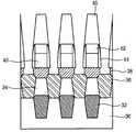
도 1 은 종래기술에 따른 반도체소자의 제조방법을 도시한 단면도이다.1 is a cross-sectional view showing a method of manufacturing a semiconductor device according to the prior art.
먼저, 반도체기판(10)에서 소자분리영역으로 예정되는 부분에 소자분리절연막(12)을 형성하고, 전체표면 상부에 게이트절연막(도시 안됨)을 형성하고, 게이트전극과 소오스/드레인접합영역으로 구성되는 모스 전계효과 트랜지스터를 형성한다.First, a device
다음, 전체표면 상부에 상기 반도체기판(10)에서 비트라인 콘택플러그 및 저장전극 콘택플러그로 예정되는 부분을 노출시키는 제1층간절연막(14)을 형성한다.Next, a first
그 다음, 전체표면 상부에 콘택플러그용 도전층을 형성하고, 화학적 기계적 연마공정 또는 전면식각공정으로 평탄화시켜 콘택플러그(14)를 형성한다.Then, the contact plug conductive layer is formed on the entire surface, and the
다음, 전체표면 상부에 상기 콘택플러그(14)에서 비트라인 콘택으로 예정되는 부분을 노출시키는 비트라인 콘택홀이 구비된 제2층간절연막(18)을 형성하고, 상기 비트라인 콘택홀을 통하여 상기 콘택플러그(14)에 접속되는 비트라인 콘택(도 시 안됨)을 형성한다. 이때, 상기 제2층간절연막(18)은 고밀도 플라즈마 산화막(high desity plasma oxide)으로 형성한다.Next, a second
그 다음, 상기 비트라인 콘택에 접속되는 비트라인(20)을 형성하되, 상기 비트라인(20)의 상부에는 마스크절연막패턴(22)이 적층되고, 그 측벽에는 절연막 스페이서(24)가 형성된다.Next, a
다음, 전체표면 상부에 제3층간절연막(25)을 형성하고, 저장전극 콘택마스크를 식각마스크로 상기 제3층간절연막(25)과 제2층간절연막(18)을 식각하여 저장전극 콘택홀(도시 안됨)을 형성한다. 상기 제3층간절연막(25)은 BPSG막으로 형성한다.Next, a third interlayer
그 다음, 전체표면 상부에 저장전극 콘택용 도전층을 형성하여 상기 저장전극 콘택홀을 매립시킨 후 평탄화시켜 상기 콘택플러그(14)에 접속되는 저장전극 콘택(25)을 형성한다.Next, a conductive layer for storage electrode contacts is formed on the entire surface to fill the storage electrode contact holes, and then planarize to form
상기 종래기술에 따른 반도체소자의 제조방법은, 저장전극 콘택홀을 자기정렬콘택식각방법을 이용하여 형성하고 있으나, 이 방법은 공정의 안정성 및 공정 수율 측면에서 유리하지만 콘택 면적을 확보하는 데 있어서 매우 취약하기 때문에 자기졍렬콘택 식각공정 시 발생한 경사를 식각 프로파일에 의해 콘택플러그와 만나는 부분에 충분한 면적을 확보하기 어렵고 그로 인하여 콘택 저항이 증가하는 등 소자의 동작특성을 저하시키는 문제점이 있다.In the semiconductor device manufacturing method according to the prior art, the storage electrode contact hole is formed using a self-aligned contact etching method, but this method is advantageous in terms of process stability and process yield, but is very effective in securing contact area. Because of the fragility, it is difficult to secure a sufficient area at the portion where the inclination generated during the self-array contact etching process meets the contact plug by the etching profile, and thus, there is a problem of deteriorating the operating characteristics of the device such as an increase in contact resistance.
본 발명은 상기와 같은 문제점을 해결하기 위한 것으로서, 저장전극 콘택을 형성하기 전에 형성되는 층간절연막을 식각선택비 차이를 갖는 박막으로 형성하되, 저장전극 콘택홀을 형성하기 위한 식각공정 후 세정공정을 추가로 실시하여 저장전극 콘택홀 저부에 형성된 층간절연막이 측면으로 식각되게 하여 저장전극 콘택홀 저부의 면적을 증가시킴으로써 콘택 저항 특성을 향상시키는 반도체소자의 제조방법을 제공함에 있다.The present invention is to solve the above problems, the interlayer insulating film formed before forming the storage electrode contact to form a thin film having an etching selectivity difference, the cleaning process after the etching process for forming the storage electrode contact hole In addition, the present invention provides a method of manufacturing a semiconductor device that improves contact resistance characteristics by increasing the area of the bottom of the storage electrode contact hole by etching the interlayer insulating layer formed on the bottom of the storage electrode contact hole.
상기와 같은 목적을 달성하기 위한 본 발명에 따른 반도체소자의 제조방법의 특징은,Features of the semiconductor device manufacturing method according to the present invention for achieving the above object,
반도체기판 상부에 소자분리절연막 및 모스 전계효과 트랜지스터 등의 하부구조물을 형성하고, 전체표면 상부에 상기 반도체기판에서 비트라인 콘택플러그 및 저장전극 콘택으로 예정되는 부분에 접속되는 콘택플러그가 구비된 제1층간절연막패턴을 형성하는 공정과,A first structure having a lower structure such as a device isolation insulating film and a MOS field effect transistor formed on the semiconductor substrate, and having a contact plug connected to a portion of the semiconductor substrate, the bit line contact plug and the storage electrode contact, on the entire surface of the semiconductor substrate; Forming an interlayer insulating film pattern;
전체표면 상부에 상기 콘택플러그 중에서 비트라인 콘택으로 예정되는 부분에 접속되는 비트라인 콘택이 구비된 제2층간절연막을 형성하는 공정과,Forming a second interlayer insulating film having a bit line contact connected to a portion of the contact plug, which is supposed to be a bit line contact, over the entire surface thereof;
상기 비트라인 콘택에 접속되는 비트라인을 형성하는 공정과,Forming a bit line connected to the bit line contact;
상기 비트라인의 측벽에 절연막 스페이서를 형성하는 공정과,Forming an insulating film spacer on sidewalls of the bit lines;
전체표면 상부에 제3층간절연막을 형성하는 공정과,Forming a third interlayer insulating film over the entire surface;
상기 콘택플러그 중에서 저장전극 콘택으로 예정되는 부분을 노출시키는 저장전극 콘택마스크를 식각마스크로 상기 제3, 제2층간절연막을 식각하여 저장전극 콘택홀을 형성하는 공정과,Forming a storage electrode contact hole by etching the third and second interlayer insulating layers using an etching mask of a storage electrode contact mask that exposes a portion of the contact plug that is intended to be a storage electrode contact;
상기 구조를 세정하되, 상기 세정공정으로 상기 저장전극 콘택홀 저부의 제2층간절연막이 측면 식각되어 콘택 면적을 증가시키는 공정과,Cleaning the structure, wherein the second interlayer dielectric layer of the bottom of the storage electrode contact hole is etched laterally to increase the contact area;
상기 저장전극 콘택홀을 매립하는 저장전극 콘택을 형성하는 것을 특징으로 한다.And forming a storage electrode contact to fill the storage electrode contact hole.
이하, 본 발명에 따른 반도체소자의 제조방법에 관하여 첨부 도면을 참조하여 상세히 설명한다.Hereinafter, a method of manufacturing a semiconductor device according to the present invention will be described in detail with reference to the accompanying drawings.
도 2 는 본 발명에 따른 반도체소자의 제조방법의 원리를 나타내는 TEM사진으로서, 비트라인을 형성하고, 비트라인 콘택의 프로파일을 나타내는 것으로, ⓐ와 ⓑ. 사이에 단차가 발생한 것을 알 수 있는데, 이는 전 공정에서 형성되는 층간절연막들의 식각선택비가 다르기 때문에 비트라인 콘택 식각 후 비트라인 방지막 형성 전 세정공정을 실시한 경우 식각속도 차이에 의해 단차가 발생한 것을 나타낸다.Figure 2 is a TEM photograph showing the principle of the method of manufacturing a semiconductor device according to the present invention, forming a bit line, showing the profile of the bit line contacts, ⓐ and ⓑ. It can be seen that a step is generated between the layers, which indicates that the step is caused by the difference in etching speed when the cleaning process is performed after the bit line contact etching is performed after the etching selectivity of the interlayer insulating layers formed in the previous step is different.
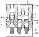
도 3a 내지 도 3c 는 본 발명에 따른 반도체소자의 제조방법을 도시한 단면도이다.3A to 3C are cross-sectional views illustrating a method of manufacturing a semiconductor device according to the present invention.
먼저, 반도체기판(30)에서 소자분리영역으로 예정되는 부분에 소자분리절연막(32)을 형성하고, 전체표면 상부에 게이트절연막(도시 안됨)을 형성하고, 게이트전극과 소오스/드레인접합영역으로 구성되는 모스 전계효과 트랜지스터를 형성한다.First, a device
다음, 전체표면 상부에 상기 반도체기판(30)에서 비트라인 콘택플러그 및 저장전극 콘택플러그로 예정되는 부분을 노출시키는 제1층간절연막(34)을 형성한다.Next, a first
그 다음, 전체표면 상부에 콘택플러그용 도전층을 형성하고, 화학적 기계적 연마공정 또는 전면식각공정으로 평탄화시켜 콘택플러그(36)를 형성한다.Then, the contact plug conductive layer is formed on the entire surface, and the
다음, 전체표면 상부에 상기 콘택플러그(36)에서 비트라인 콘택으로 예정되는 부분을 노출시키는 비트라인 콘택홀이 구비된 제2층간절연막(38)을 형성하고, 상기 비트라인 콘택홀을 통하여 상기 콘택플러그(36)에 접속되는 비트라인 콘택(도시 안됨)을 형성한다. 이때, 상기 제2층간절연막(38)은 후속 세정공정에서 선택적인 식각을 위해 식각속도가 빠른 BPSG막, PSG막 또는 BSG막과 같이 불순물이 주입된 산화막 또는 SOG막으로 형성한다.Next, a second
그 다음, 상기 비트라인 콘택에 접속되는 비트라인(40)을 형성하되, 상기 비트라인(40)의 상부에는 마스크절연막패턴(42)이 적층되고, 그 측벽에는 절연막 스페이서(44)가 형성된다.Next, a
다음, 전체표면 상부에 제3층간절연막(45)을 형성하고, 저장전극 콘택마스크를 식각마스크로 상기 제3층간절연막(45)과 제2층간절연막(38)을 식각하여 저장전극 콘택홀(46)을 형성한다. 이때, 상기 제3층간절연막(45)은 상기 제2층간절연막(38)보다 식각선택비가 작은 산화막으로 형성하거나, 상기 제2층간절연막(38)과 같이 BPSG막, PSG막 또는 BSG막과 같이 불순물이 주입된 산화막 또는 SOG막으로 형성할 수 있다.Next, a third
그 후, 세정공정을 실시하여 상기 저장전극 콘택홀(46) 저부의 제2층간절연막(38)이 측면으로 식각되게 함으로써 저장전극 콘택홀(46) 저부의 면적을 증가시킨다. 이때, 상기 세정공정은 205 ∼ 300 : 1의 BOE(buffer of etchant)용액에서 15 ∼ 25초 간 실시한다.Thereafter, a cleaning process is performed to etch the second
그 다음, 전체표면 상부에 저장전극 콘택용 도전층을 형성하여 상기 저장전극 콘택홀(46)을 매립시킨 후 평탄화시켜 상기 콘택플러그(36)에 접속되는 저장전극 콘택(48)을 형성한다. (도 3c 참조)Next, a storage electrode contact conductive layer is formed on the entire surface to fill the storage
이상에서 설명한 바와 같이, 본 발명에 따른 반도체소자의 제조방법은, 반도체기판 상부에 모스 전계효과 트랜지스터를 형성하고, 전체표면 상부에 비트라인 콘택플러그 및 저장전극 콘택플러그를 구비하는 제1층간절연막을 형성한 다음, 전체표면 상부에 상기 비트라인 콘택플러그에 접속되는 비트라인 콘택이 구비된 제2층간절연막을 형성하되, 상기 제2층간절연막을 식각속도가 빠른 산화막으로 형성한 후, 상기 비트라인 콘택에 접속되는 비트라인을 형성한 다음, 제3층간절연막을 형성하고 저장전극 콘택마스크를 식각마스크로 상기 제3층간절연막과 제2층간절연막을 식각하여 저장전극 콘택홀을 형성한 후 세정공정을 실시하여 상기 제2층간절연막을 측면식각함으로써 저장전극 콘택홀 저부의 면적을 증가시킴으로써 콘택 저항 특성을 향상시킬 수 있는 이점이 있다.As described above, the method for manufacturing a semiconductor device according to the present invention includes forming a MOS field effect transistor on an upper surface of a semiconductor substrate, and forming a first interlayer insulating layer having a bit line contact plug and a storage electrode contact plug on an entire surface thereof. After forming, a second interlayer insulating film having a bit line contact connected to the bit line contact plug is formed on the entire surface, and the second interlayer insulating film is formed of an oxide film having a high etching rate, and then the bit line contact is formed. After forming the bit line connected to the insulating film, a third interlayer insulating film is formed, and the third interlayer insulating film and the second interlayer insulating film are etched using the storage electrode contact mask as an etch mask to form a storage electrode contact hole, and then a cleaning process is performed. By etching the second interlayer insulating layer side by side to increase the area of the bottom of the storage electrode contact hole to improve the contact resistance characteristics There is an advantage to this.
Claims (3)
Translated fromKoreanPriority Applications (1)
| Application Number | Priority Date | Filing Date | Title |
|---|---|---|---|
| KR1020000036920AKR100596831B1 (en) | 2000-06-30 | 2000-06-30 | Manufacturing method of semiconductor device |
Applications Claiming Priority (1)
| Application Number | Priority Date | Filing Date | Title |
|---|---|---|---|
| KR1020000036920AKR100596831B1 (en) | 2000-06-30 | 2000-06-30 | Manufacturing method of semiconductor device |
Publications (2)
| Publication Number | Publication Date |
|---|---|
| KR20020002680A KR20020002680A (en) | 2002-01-10 |
| KR100596831B1true KR100596831B1 (en) | 2006-07-04 |
Family
ID=19675217
Family Applications (1)
| Application Number | Title | Priority Date | Filing Date |
|---|---|---|---|
| KR1020000036920AExpired - Fee RelatedKR100596831B1 (en) | 2000-06-30 | 2000-06-30 | Manufacturing method of semiconductor device |
Country Status (1)
| Country | Link |
|---|---|
| KR (1) | KR100596831B1 (en) |
Families Citing this family (5)
| Publication number | Priority date | Publication date | Assignee | Title |
|---|---|---|---|---|
| KR100450671B1 (en)* | 2002-02-26 | 2004-10-01 | 삼성전자주식회사 | Method for fabricating semiconductor device having storage node contact plugs |
| KR100439034B1 (en)* | 2002-08-02 | 2004-07-03 | 삼성전자주식회사 | Bitline of semiconductor device with leakage current protection and method for forming the same |
| KR100557994B1 (en) | 2003-07-25 | 2006-03-06 | 삼성전자주식회사 | Semiconductor device having buried extension contact hole and manufacturing method thereof |
| KR100755673B1 (en)* | 2006-08-04 | 2007-09-05 | 삼성전자주식회사 | Semiconductor device manufacturing method and semiconductor device manufactured accordingly |
| KR101368803B1 (en) | 2007-10-02 | 2014-02-28 | 삼성전자주식회사 | Semiconductor memory device and the method of forming the same |
- 2000
- 2000-06-30KRKR1020000036920Apatent/KR100596831B1/ennot_activeExpired - Fee Related
Also Published As
| Publication number | Publication date |
|---|---|
| KR20020002680A (en) | 2002-01-10 |
Similar Documents
| Publication | Publication Date | Title |
|---|---|---|
| KR100474546B1 (en) | Fabricating method for semiconductor device | |
| US6528418B1 (en) | Manufacturing method for semiconductor device | |
| KR100465596B1 (en) | A manufacturing method for semiconductor device | |
| KR100596831B1 (en) | Manufacturing method of semiconductor device | |
| KR100726148B1 (en) | Manufacturing method of semiconductor device | |
| KR20010063761A (en) | Fabricating method for semiconductor device | |
| KR100420413B1 (en) | Manufacturing method for semiconductor device | |
| KR100324023B1 (en) | Manufacturing method of semiconductor device | |
| KR100345367B1 (en) | Fabricating method for semiconductor device | |
| KR100709453B1 (en) | Bit line formation method of semiconductor device | |
| KR100333548B1 (en) | Fabricating method for semiconductor device | |
| KR20030058573A (en) | Manufacturing method for semiconductor device | |
| KR100944344B1 (en) | Manufacturing method of semiconductor device | |
| KR100546192B1 (en) | Manufacturing method of semiconductor device | |
| KR100433093B1 (en) | Manufacturing method of semiconductor device | |
| KR100304440B1 (en) | Manufacturing method of semiconductor device | |
| KR20030058635A (en) | Manufacturing method for semiconductor device | |
| KR20010063856A (en) | Fabricating method for semiconductor device | |
| KR100527531B1 (en) | Manufacturing method for semiconductor device | |
| KR20000043205A (en) | Method for forming contact hole of semiconductor device | |
| KR20010005156A (en) | Fabricating method for semiconductor device | |
| KR20000027639A (en) | Method for manufacturing contact plug of semiconductor devices | |
| KR20010005227A (en) | Fabricating method for semiconductor device | |
| KR20020095910A (en) | Manufacturing method for semiconductor device | |
| KR20030059416A (en) | Manufacturing method for semiconductor device |
Legal Events
| Date | Code | Title | Description |
|---|---|---|---|
| PA0109 | Patent application | St.27 status event code:A-0-1-A10-A12-nap-PA0109 | |
| PN2301 | Change of applicant | St.27 status event code:A-3-3-R10-R13-asn-PN2301 St.27 status event code:A-3-3-R10-R11-asn-PN2301 | |
| PN2301 | Change of applicant | St.27 status event code:A-3-3-R10-R13-asn-PN2301 St.27 status event code:A-3-3-R10-R11-asn-PN2301 | |
| PG1501 | Laying open of application | St.27 status event code:A-1-1-Q10-Q12-nap-PG1501 | |
| A201 | Request for examination | ||
| PA0201 | Request for examination | St.27 status event code:A-1-2-D10-D11-exm-PA0201 | |
| E701 | Decision to grant or registration of patent right | ||
| PE0701 | Decision of registration | St.27 status event code:A-1-2-D10-D22-exm-PE0701 | |
| PR1002 | Payment of registration fee | St.27 status event code:A-2-2-U10-U11-oth-PR1002 Fee payment year number:1 | |
| GRNT | Written decision to grant | ||
| PR0701 | Registration of establishment | St.27 status event code:A-2-4-F10-F11-exm-PR0701 | |
| PG1601 | Publication of registration | St.27 status event code:A-4-4-Q10-Q13-nap-PG1601 | |
| R17-X000 | Change to representative recorded | St.27 status event code:A-5-5-R10-R17-oth-X000 | |
| PR1001 | Payment of annual fee | St.27 status event code:A-4-4-U10-U11-oth-PR1001 Fee payment year number:4 | |
| PR1001 | Payment of annual fee | St.27 status event code:A-4-4-U10-U11-oth-PR1001 Fee payment year number:5 | |
| FPAY | Annual fee payment | Payment date:20110526 Year of fee payment:6 | |
| PR1001 | Payment of annual fee | St.27 status event code:A-4-4-U10-U11-oth-PR1001 Fee payment year number:6 | |
| PN2301 | Change of applicant | St.27 status event code:A-5-5-R10-R13-asn-PN2301 St.27 status event code:A-5-5-R10-R11-asn-PN2301 | |
| LAPS | Lapse due to unpaid annual fee | ||
| PC1903 | Unpaid annual fee | St.27 status event code:A-4-4-U10-U13-oth-PC1903 Not in force date:20120628 Payment event data comment text:Termination Category : DEFAULT_OF_REGISTRATION_FEE | |
| PN2301 | Change of applicant | St.27 status event code:A-5-5-R10-R13-asn-PN2301 St.27 status event code:A-5-5-R10-R11-asn-PN2301 | |
| PC1903 | Unpaid annual fee | St.27 status event code:N-4-6-H10-H13-oth-PC1903 Ip right cessation event data comment text:Termination Category : DEFAULT_OF_REGISTRATION_FEE Not in force date:20120628 | |
| PN2301 | Change of applicant | St.27 status event code:A-5-5-R10-R13-asn-PN2301 St.27 status event code:A-5-5-R10-R11-asn-PN2301 | |
| P22-X000 | Classification modified | St.27 status event code:A-4-4-P10-P22-nap-X000 | |
| P22-X000 | Classification modified | St.27 status event code:A-4-4-P10-P22-nap-X000 |