KR100594385B1 - Nonvolatile Memory Devices - Google Patents
Nonvolatile Memory DevicesDownload PDFInfo
- Publication number
- KR100594385B1 KR100594385B1KR1020030101092AKR20030101092AKR100594385B1KR 100594385 B1KR100594385 B1KR 100594385B1KR 1020030101092 AKR1020030101092 AKR 1020030101092AKR 20030101092 AKR20030101092 AKR 20030101092AKR 100594385 B1KR100594385 B1KR 100594385B1
- Authority
- KR
- South Korea
- Prior art keywords
- gate
- floating gate
- memory device
- oxide film
- threshold voltage
- Prior art date
- Legal status (The legal status is an assumption and is not a legal conclusion. Google has not performed a legal analysis and makes no representation as to the accuracy of the status listed.)
- Expired - Fee Related
Links
Images


Classifications
- H—ELECTRICITY
- H10—SEMICONDUCTOR DEVICES; ELECTRIC SOLID-STATE DEVICES NOT OTHERWISE PROVIDED FOR
- H10B—ELECTRONIC MEMORY DEVICES
- H10B41/00—Electrically erasable-and-programmable ROM [EEPROM] devices comprising floating gates
- H10B41/30—Electrically erasable-and-programmable ROM [EEPROM] devices comprising floating gates characterised by the memory core region
- H—ELECTRICITY
- H10—SEMICONDUCTOR DEVICES; ELECTRIC SOLID-STATE DEVICES NOT OTHERWISE PROVIDED FOR
- H10D—INORGANIC ELECTRIC SEMICONDUCTOR DEVICES
- H10D30/00—Field-effect transistors [FET]
- H10D30/01—Manufacture or treatment
- H10D30/021—Manufacture or treatment of FETs having insulated gates [IGFET]
- H10D30/0411—Manufacture or treatment of FETs having insulated gates [IGFET] of FETs having floating gates
- H—ELECTRICITY
- H10—SEMICONDUCTOR DEVICES; ELECTRIC SOLID-STATE DEVICES NOT OTHERWISE PROVIDED FOR
- H10D—INORGANIC ELECTRIC SEMICONDUCTOR DEVICES
- H10D30/00—Field-effect transistors [FET]
- H10D30/60—Insulated-gate field-effect transistors [IGFET]
- H10D30/68—Floating-gate IGFETs
- H10D30/6891—Floating-gate IGFETs characterised by the shapes, relative sizes or dispositions of the floating gate electrode
- H10D30/6892—Floating-gate IGFETs characterised by the shapes, relative sizes or dispositions of the floating gate electrode having at least one additional gate other than the floating gate and the control gate, e.g. program gate, erase gate or select gate
Landscapes
- Non-Volatile Memory (AREA)
Abstract
Translated fromKoreanDescription
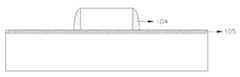
Translated fromKorean도 1은 종래 기술에 의한 플래시 메모리 셀의 단면도.1 is a cross-sectional view of a flash memory cell according to the prior art.
도 2 내지 도 6은 본 발명에 따른 비휘발성 메모리 소자의 제조방법을 나타낸 공정단면도.2 to 6 are cross-sectional views illustrating a method of manufacturing a nonvolatile memory device according to the present invention.
도 7은 본 발명에 의한 비휘발성 메모리 소자의 프로그램/이레이즈 특성을 나타낸 도면.7 is a diagram showing program / erase characteristics of a nonvolatile memory device according to the present invention.
도 8은 본 발명에 의한 비휘발성 메모리 소자의 멀티 레벨 비트 문턱 전압 분포를 나타낸 도면.8 is a diagram illustrating a multi-level bit threshold voltage distribution of a nonvolatile memory device according to the present invention.
도 9은 본 발명에 따른 비휘발성 메모리 소자의 셀 어레이.9 is a cell array of a nonvolatile memory device according to the present invention.
도 10은 본 발명에 의한 비휘발성 메모리 소자의 셀 레이아웃.10 is a cell layout of a nonvolatile memory device according to the present invention.
도 11는 도 10의 A-A' 방향으로 자를 경우 단면도.FIG. 11 is a cross-sectional view taken along the line AA ′ of FIG. 10;
도 12은 도 10의 B-B' 방향으로 자를 경우 경우의 단면도.12 is a cross-sectional view when cutting in the direction BB ′ of FIG. 10.
본 발명은 비휘발성 메모리 소자에 관한 것으로, 보다 자세하게는 내구 특성과 리텐션 특성이 우수한 인젝션 게이트를 가지는 비휘발성 메모리 소자에 관한 것이다.The present invention relates to a nonvolatile memory device, and more particularly, to a nonvolatile memory device having an injection gate having excellent durability and retention characteristics.
일반적으로 반도체 메모리 장치는 크게 휘발성 메모리(volatile memory)와 비휘발성 메모리(non-volatile memory)로 구분된다. 휘발성 메모리의 대부분은 DRAM(Dynamic Random Access Memory), SRAM(Static Random Access Memory) 등의 RAM이 차지하고 있으며, 전원 인가시 데이타의 입력 및 보존이 가능하지만, 전원 제거시 데이타가 휘발되어 보존이 불가능한 특징을 가진다. 반면에, ROM(Read Only Memory)이 대부분을 차지하고 있는 비휘발성 메모리는 전원이 인가되지 않아도 데이타가 보존되는 특징을 가진다.In general, semiconductor memory devices are classified into volatile memory and non-volatile memory. Most of volatile memory is occupied by RAM such as DRAM (Dynamic Random Access Memory) and SRAM (Static Random Access Memory), and data can be input and stored when power is applied, but data cannot be saved because of volatilization when power is removed. Has On the other hand, nonvolatile memory, which is mostly occupied by ROM (Read Only Memory), is characterized in that data is preserved even when power is not applied.
현재, 공정기술 측면에서 비휘발성 메모리 장치는 플로팅 게이트(Floationg Gate) 계열과 두 종류 이상의 유전막이 2중 또는 3중으로 적층된 MIS(Metal Insulator Semiconductor) 계열로 구분된다.At present, in terms of process technology, a nonvolatile memory device is classified into a floating gate series and a metal insulator semiconductor (MIS) series in which two or more dielectric layers are stacked in two or three layers.
플로팅 게이트 계열의 메모리 장치는 전위 우물(potential well)을 이용하여 기억 특성을 구현하며, 현재 플래시 EEPROM(Electrically Erasable 프로그램mable Read Only Memory)으로 가장 널리 응용되고 있는 단순 적층 구조의 ETOX(EPROM Tunnel Oxide) 구조와 하나의 셀에 두 개의 트랜지스터가 구비된 채널 분리(Split gate) 구조를 들 수 있다.Floating gate series memory devices use potential wells to implement memory characteristics, and the simple stack-type EPROM Tunnel Oxide (ETOX), which is currently widely used as a flash electrically erasable programmable read only memory (EEPROM). And a split gate structure in which one transistor includes two transistors.
반면에 MIS 계열은 유전막 벌크, 유전막-유전막 계면 및 유전막-반도체 계면에 존재하는 트랩(trap)을 이용하여 기억 기능을 수행한다. 현재 플래시 EEPROM으 로 주로 응용되고 있는 MONOS/SONOS(Metal/Silicon ONO Semiconductor)구조가 대표적인 예이다.On the other hand, the MIS series performs a memory function by using traps present at the dielectric bulk, the dielectric film-dielectric film interface, and the dielectric film-semiconductor interface. A typical example is the MONOS / SONOS (Metal / Silicon ONO Semiconductor) structure, which is mainly used as a flash EEPROM.
종래 기술의 플래시 메모리 셀의 제조 방법을 도 1 에서 간략하게 설명하면, 소자 분리막(11)이 형성된 반도체 기판(10) 상부에 게이트 산화막(12)을 형성하고 그 위에 제 1 폴리실리콘층(13)을 형성하여 플로팅 게이트로 사용한다. 이 플로팅 게이트(13) 상부에 유전체층(15)과 제 2 폴리실리콘층(16)을 형성하여 이 제 2 폴리실리콘층(16)을 콘트롤 게이트로 사용한다. 이 콘트롤 게이트(16) 상부에 금속층(17)과 질화막(18)을 형성하고 셀 구조로 패터닝하여 플래시 메모리 셀을 형성한다.A method of manufacturing a flash memory cell of the prior art will be briefly described with reference to FIG. 1. The
상기와 같은 종래의 플래시 메모리 셀에서는, 플로팅 게이트와 콘트롤 게이트를 평판 형태로 형성하였다. 그러나, 플래시 메모리에서는, 콘트롤 게이트의 전위가 플로팅 게이트에 잘 전달되는 것이 소자의 소거 및 프로그램 특성을 향상시키는 데에 매우 중요하다. 왜냐하면, 플래시 메모리의 핫 캐리어(hot carrier)를 이용한 프로그램 동작시, 소오스에 0V, 드레인에 5V 및 콘트롤 게이트에 9V를 인가하는데, 콘트롤 게이트에 인가한 전압이 플로팅 게이트를 거쳐 그 전압 그대로 게이트 산화막에 전계를 만들면 더욱 빠르게 핫 전자가 플로팅 게이트로 주입된다. 반대로 소거 동작시 콘트롤 게이트에 -7V, 소오스에 약 5V를 인가하여 플로팅 게이트에 있는 전자를 F-N(Fowler-Nordheim) 터널링에 의하여 소오스 쪽으로 방출시키는데, 콘트롤 게이트와 플로팅 게이트 사이의 캐패시턴스가 크고 플로팅 게이트와 기판 사이의 캐패시턴스가 작다면 플로팅 게이트가 더욱 낮은 전압으로 유지되어 소 오스 쪽으로 전자가 더욱 많이 방출될 수 있으므로 소거 동작이 빠르게 될 수 있다. 결국, 프로그램 동작이나 소거 동작시에 플로팅 게이트의 전압이 콘트롤 게이트의 전압에 더욱 가깝게 따라 갈수록 동작이 빠르게 된다.In the conventional flash memory cell as described above, the floating gate and the control gate are formed in the form of a flat plate. However, in the flash memory, it is very important to improve the erase and program characteristics of the device that the potential of the control gate is well transferred to the floating gate. In the program operation using the hot carrier of the flash memory, 0 V is applied to the source, 5 V is applied to the drain, and 9 V is applied to the control gate, and the voltage applied to the control gate is applied to the gate oxide layer as it is through the floating gate. Creating an electric field allows hot electrons to be injected into the floating gate more quickly. In the erase operation, -7V is applied to the control gate and about 5V to the source, and electrons in the floating gate are emitted to the source by Fowler-Nordheim (FN) tunneling. The capacitance between the control gate and the floating gate is large and the floating gate and If the capacitance between the substrates is small, the floating gate can be kept at a lower voltage, which can release more electrons toward the source, resulting in faster erase operations. As a result, the operation becomes faster as the voltage of the floating gate becomes closer to the voltage of the control gate during the program operation or the erase operation.
반도체 소자의 프로그램 및 소거 특성을 향상시키는 방법으로서 플로팅 게이트와 콘트롤 게이트 사이의 유전체층으로 고유전율의 물질을 사용하는 방법이 있다. 그러나 이러한 방법은 기술적으로 개발되어야 할 부분이 상당히 많은 분야이다.As a method of improving program and erase characteristics of a semiconductor device, there is a method of using a high dielectric constant material as a dielectric layer between a floating gate and a control gate. However, these methods have a lot of technical areas to be developed.
상기 종래의 비휘발성 소자 경우 열 전자 주입(Hot Electron Injection)방식에 의한 프로그램 과정을 계속 수행함에 따라 열 전자에 의해 터널 산화막과 실리콘 기판의 계면, 터널 산화막 내부 또는 터널 산화막과 플로팅 게이트 계면 사이에 트랩 사이트가 생기게 되고 이러한 트랩 사이트에 의해 문턱 전압이 변화하게 된다. 또한 상기 트랩 사이트가 저장된 전하들이 빠져나가는 통로 역할을 하게 되어 저장된 전하가 빨리 소실된다. 즉 내구(Endurance) 특성과 리텐션(Retention) 특성에 문제가 있다.In the conventional nonvolatile device, as the programming process is performed by hot electron injection, hot electrons trap the interface between the tunnel oxide film and the silicon substrate, the tunnel oxide film, or between the tunnel oxide film and the floating gate interface. Sites are created and these trap sites cause threshold voltages to change. In addition, the trap site serves as a passage through which the stored charges are discharged, and thus the stored charge is quickly lost. That is, there is a problem in endurance characteristics and retention characteristics.
따라서, 본 발명은 상기와 같은 종래 기술의 문제점을 해결하기 위한 것으로, 내구 특성과 리텐션 특성이 우수하며 이레이지 문턱전압을 일정값으로 수렴시킬 수 있는 셀프 컨버전스 이레이즈 특성을 가지는 인젝션 게이트를 포함하는 트랜지스터와 오버 이레이즈 문제, 드레인 턴온현상, 드레인 디스터브 등과 같은 문제 를 제거할 수 있는 셀렉트 트랜지스터를 포함하는 노어 플래시 셀의 어레이를 효과적으로 구현하기 위한 비휘발성 메모리 소자를 제공함에 본 발명의 목적이 있다.
Accordingly, the present invention is to solve the problems of the prior art as described above, and includes an injection gate having excellent durability characteristics and retention characteristics and having a self-converging erasure characteristic capable of converging an erasure threshold voltage to a predetermined value. SUMMARY OF THE INVENTION An object of the present invention is to provide a nonvolatile memory device for effectively implementing an array of NOR flash cells including a transistor and a select transistor capable of eliminating problems such as over erasure, drain turn-on, and drain disturb. .
본 발명의 상기 목적은 반도체 기판에 나란히 배치된 다수의 활성 영역; 상기 활성 영역을 가로지르는 다수의 콘트롤 게이트; 상기 콘트롤 게이트와 평형으로 이격되어 상기 활성 영역들 상부를 가로지르는 셀렉트 게이트; 상기 각각의 활성 영역과 상기 각각의 콘트롤 게이트 사이에 형성된 플로팅 게이트; 상기 플로팅 게이트의 일측 하부와 상기 활성 영역 사이에 형성된 인젝션 게이트; 상기 콘트롤 게이트와 플로팅 게이트 사이에 개재된 블럭 산화막; 상기 플로팅 게이트의 일측 하부에 형성된 소오스 영역; 상기 셀렉트 게이트의 양측 하부에 형성된 드레인 영역 및 상기 플로팅 게이트와 인접하지 않은 드레인 영역에 형성된 비트 라인 콘택을 포함하는 것을 특징으로 하는 비휘발성 메모리 소자에 의해 달성된다.The object of the invention is a plurality of active regions disposed side by side on a semiconductor substrate; A plurality of control gates across the active region; A select gate disposed in equilibrium with the control gate and across the active regions; A floating gate formed between the respective active regions and the respective control gates; An injection gate formed between a lower side of one side of the floating gate and the active region; A block oxide film interposed between the control gate and the floating gate; A source region formed under one side of the floating gate; And a bit line contact formed in a drain region formed under both sides of the select gate and a drain region not adjacent to the floating gate.
본 발명의 상기 목적과 기술적 구성 및 그에 따른 작용효과에 관한 자세한 사항은 본 발명의 바람직한 실시예를 도시하고 있는 도면을 참조한 이하 상세한 설명에 의해 보다 명확하게 이해될 것이다.Details of the above object and technical configuration of the present invention and the effects thereof according to the present invention will be more clearly understood by the following detailed description with reference to the drawings showing preferred embodiments of the present invention.
도 2 내지 도 6은 본 발명에 따른 비휘발성 메모리 소자의 제조방법을 나타낸 공정단면도이다.2 to 6 are process cross-sectional views illustrating a method of manufacturing a nonvolatile memory device according to the present invention.
먼저, 도 2에 도시된 바와 같이, P형 실리콘 기판(101) 위에 패드 산화막(102)과 질화막(103)을 차례로 성장 내지는 증착한 후 상기 질화막을 패터닝 한다. 상기 질화막의 패터닝시 비휘발성 메모리 소자의 드레인 영역에만 질화막을 남겨두고 나머지 영역의 질화막은 모두 제거한다. 상기 질화막은 산화막 내지 기타 절연막으로 대치할 수 있으며, 상기 질화막은 500 내지 2500Å의 두께로 증착하는 것이 바람직하다.First, as shown in FIG. 2, the
다음, 도 3에 도시된 바와 같이, 인젝션 게이트를 형성한다. 질화막이 에칭된 영역에 남아 있는 패드 산화막을 모두 제거한 후 산화공정을 통해 터널 산화막(105)을 50Å 내지 120Å의 두께로 성장시킨다. 이후 인젝션 게이트를 형성하기 위해 밴드갭(Band Gap)이 실리콘 기판보다 크고 터널 산화막(SiO2)보다 작은 인젝션 게이트용 막질을 기판의 전면에 100Å 내지 1000Å의 두께로 증착한다. 상기 인젝션 게이트용 막질을 웨이퍼 전면에 증착한 후 비등방성 블랭킷 식각으로 질화막의 측벽에 사이드월 형태의 인젝션 게이트(104)를 형성시킨다. 상기 인젝션 게이트용 막질은 밴드갭이 1.1eV 보다 크고 9.0 eV 보다 작은 물질이면 모두 사용이 가능하고, 보다 바람직하게는 Al2O3, Y2O3, HfO2, ZrO2, BaZrO2, BaTiO3, Ta2O5, CaO, SrO, BaO, La2O3, Ce2O3, Pr2O3, Nd2O3, Pm2O3, Sm2O3, Eu2O3, Gd2O3, Tb2O3, Dy2O3, Ho2O3, Er2O3, Tm2O3, Yb2O3 또는 Lu2O3등과 같은 산화막과 SiC, AlP, AlAs, AlSb, GaP, GaAs, InP, ZnS, ZnSe, ZnTe, CdS, CdSe, CdTe 등과 같은 화합물 반도체를 사용할 수 있다.Next, as shown in FIG. 3, an injection gate is formed. After removing all of the pad oxide film remaining in the nitride-etched region, the
다음, 도 4에 도시된 바와 같이, 제 1 폴리실리콘, 블럭 산화막, 제 2 폴리 실리콘을 증착한다. 웨이퍼 전면에 플로팅 게이트용 폴리 실리콘(106)을 증착하고 상기 폴리 실리콘의 상부에 블럭 산화막(107)을 형성한다. 이어 상기 블럭 산화막의 상부에 콘트롤 게이트용 폴리 실리콘(108)을 증착한다. 상기 플로팅 게이트용 폴리 실리콘과 콘트롤 게이트용 폴리 실리콘은 모두 N형의 불순물로 도핑된 폴리 실리콘이거나 증착한 후 N형으로 도핑시킨다. 상기 터널 산화막은 인젝션 게이트 형성시 손상을 입을 가능성이 있으므로 플로팅 게이트용 폴리 실리콘을 증착하기 전에 남아 있는 터널 산화막을 제거하고 다시 증착할 수도 있다. 상기 블럭 산화막은 제 1 블럭 산화막(107a)과 제 2 블럭 산화막(107b)로 구성되며, 상기 제 1 블럭 산화막은 Al2O3나 Y2O3를 사용하며 상기 제 2블럭 산화막은 SiO2를 사용한다. 상기 블럭 산화막의 두께는 수렴하고자 하는 이레이즈의 문턱 전압과 터널 산화막의 두께에 의해 결정되는데, 바람직하게는 제 1 블럭 산화막은 50 내지 250Å, 제 2 블럭 산화막은 20 내지 150Å의 두께로 증착한다.Next, as shown in FIG. 4, the first polysilicon, the block oxide film, and the second polysilicon are deposited. A
다음, 도 5에 도시된 바와 같이, 제 2 폴리 실리콘, 블럭 산화막, 제 1 폴리 실리콘 및 질화막을 식각한 후 소오스/드레인 확장 영역을 형성한다. 상기 콘트롤 게이트용 폴리 실리콘의 상부에 포토레지스트를 도포하고 패터닝한 후 상기 패터닝된 포토레지스트를 식각 마스크로 상기 콘트롤 게이트용 폴리 실리콘, 블럭 산화막 및 플로팅 게이트용 폴리 실리콘을 식각하여 플로팅 게이트 및 콘트롤 게이트를 형성한다. 이어 상기 인젝션 게이트의 사이에 잔류하는 질화막을 제거한다. 상기 질화막은 건식식각 또는 인산을 이용한 습식식각으로 제거한다. 이어 상기 기판에 N형 불순물을 주입하여 소오스/드레인 확장 영역(109)을 형성한다.Next, as shown in FIG. 5, the second polysilicon, the block oxide film, the first polysilicon, and the nitride film are etched to form a source / drain extension region. After the photoresist is coated and patterned on the control silicon polysilicon, the control gate polysilicon, the block oxide film and the floating gate polysilicon are etched using the patterned photoresist as an etch mask to form a floating gate and a control gate. Form. Next, the nitride film remaining between the injection gates is removed. The nitride film is removed by dry etching or wet etching using phosphoric acid. Subsequently, an N-type impurity is implanted into the substrate to form a source /
다음, 도 6에 도시된 바와 같이, 사이드월 스페이서와 소오스/드레인 영역을 형성한다. 상기 기판에 사이드월 스페이서 형성을 위해 산화막(110)과 질화막(111)을 차례로 증착한 후 비등방성 식각을 통해 사이드월 스페이서를 형성한다. 이어 상기 게이트 및 사이드월 스페이서를 이온주입 마스크로 N형 불순물을 이온주입하여 소오스/드레인 영역(112)을 형성한다.Next, as shown in FIG. 6, sidewall spacers and source / drain regions are formed. The
도 7은 본 발명에 의한 비휘발성 메모리 소자의 프로그램/이레이즈 특성을 나타낸 도면이다. “00”상태를 나타내는 문턱전압을 VT1, “01”상태를 나타내는 문턱전압을 VT2, “10”상태를 나타내는 문턱전압을 VT3, “11”상태를 나타내는 문턱전압을 VT4라고 할 경우 각각의 상태로 프로그램되어 있는 셀을 이레이즈 시킬 경우 Te[sec] 이상 이레이즈 동작을 수행하면 셀들이 어떠한 상태로 프로그램되어 있든지에 상관 없이 이레이즈 문턱전압이 수렴하는 특성에 의해 VT1값으로 모두 이레이즈 문턱전압이 수렴한다.7 is a diagram illustrating program / erase characteristics of a nonvolatile memory device according to the present invention. When the threshold voltage indicating the "00" state is VT1, the threshold voltage indicating the "01" state is VT2, the threshold voltage indicating the "10" state is VT3, and the threshold voltage indicating the "11" state is VT4, respectively. When erasing the programmed cell, if the erase operation is over Te [sec], the erase threshold voltage is all erased to VT1 value due to the convergence of the erase threshold voltage regardless of the state in which the cells are programmed. This converges.
상기와 같이 이레이즈시킨 셀들을 각각 “00”, “01”, “10”, “11” 상태로 프로그램시키는 경우를 살펴보면 “00”상태로 만들 셀들은 이레이즈시킨 상태 그대로 두면 된다. “01”상태로 만들 셀들은 Tp1[sec]만큼 프로그램시킨다. “10”상태로 만들 셀들은 Tp2[sec]만큼 프로그램시킨다. “11”상태로 프로그램시킬 셀들은 Tp3[sec]만큼 프로그램시킨다. 이레이즈 상태의 문턱 전압 분포가 매우 좁기 때문에 프로그램 시킨 후의 셀들의 문턱전압 분포 역시 매우 좁게 되어 문턱 전압 윈도우 마진을 크게 만들 수 있다.Referring to the case of programming the erased cells to the states of "00", "01", "10", and "11", the cells to be made to the "00" state are left in the erased state. The cells to be put into the "01" state are programmed by Tp1 [sec]. The cells to be brought to the "10" state are programmed by Tp2 [sec]. Cells to be programmed to the “11” state are programmed by Tp3 [sec]. Since the threshold voltage distribution in the erased state is very narrow, the threshold voltage distribution of the cells after programming is also very narrow, which can increase the threshold voltage window margin.
도 8은 본 발명에 의한 비휘발성 메모리 소자의 멀티 레벨 비트 문턱 전압 분포를 나타낸 것이다. 301은 종래의 플로팅 게이트 소자의 이레이즈 상태의 문턱전압을 나타낸 것으로 오버 이레이즈에 의해 문턱전압 분포가 상당히 넓은 것을 알 수 있다. 302는 종래의 플로팅 게이트 소자의 프로그램 상태의 문턱전압을 나타낸 것으로 이레이즈 상태의 문턱 전압 분포가 매우 넓기 때문에 프로그램 상태에도 영향을 미쳐 프로그램 상태의 문턱전압 분포도 다소 넓게 분포하게 되어 이들 프로그램 상태와 이레이즈 상태의 문턱전압 윈도우(307)가 상당히 좁아져 문턱 전압 윈도우 마진이 줄어들게 된다. 따라서 종래의 플로팅 게이트 소자를 사용하여 멀티 레벨 비트 기술을 적용하기가 매우 어렵다.8 shows a multi-level bit threshold voltage distribution of a nonvolatile memory device according to the present invention. 301 shows the threshold voltage in the erased state of the conventional floating gate device, and it can be seen that the threshold voltage distribution is considerably wide due to over erasure. 302 shows the threshold voltages of the program state of the conventional floating gate device. Since the threshold voltage distribution of the erased state is very wide, the 302 also affects the program state, so that the threshold voltage distribution of the program state is also widely distributed. The
본 발명의 셀프 컨버전스 이레이즈(Self-Convergence Erase) 특성을 가지는 비휘발성 메모리 소자의 경우 이레이즈 문턱 전압의 자체 수렴특성에 의해 도면 303에 나타내어진 것과 같이 이레이즈 상태의 문턱전압 분포가 매우 좁은 특성을 지니게 된다. 이렇게 이레이즈 상태의 문턱전압이 프로그램 상태의 문턱 전압 분포에도 영향을 주어 “01”(301),”10”(305), “11”(306) 상태의 문턱 전압 분포도 좁은 것을 알 수 있다.In the case of the non-volatile memory device having the self-convergence erase characteristic of the present invention, the threshold voltage distribution in the erased state is very narrow as shown in FIG. 303 due to the self-converging characteristic of the erase threshold voltage. Will have. Thus, it can be seen that the threshold voltage of the erased state also affects the distribution of threshold voltages of the program state, so that the threshold voltage distributions of the states “01” 301, “10” 305, and “11” 306 are also narrow.
따라서 본 발명의 셀프 컨버전스 이레이즈 특성을 가지는 비휘발성 소자를 사용하여 넓은 범위의 문턱 전압 윈도우(308, 309, 310)를 얻을 수 있어 멀티 레벨 비트 기술을 쉽게 적용할 수 있다.Therefore, a wide range of
도 9는 본 발명의 셀프 컨버전스 이레이즈(Self-Convergence Erase) 특성을 가지는 비휘발성 메모리 소자를 이용하여 멀티 레벨 비트 노어형 비휘발성 메모리 셀 어레이를 구현한 도면이다.FIG. 9 illustrates a multi-level bit NOR type nonvolatile memory cell array using a nonvolatile memory device having a self-convergence erase characteristic of the present invention.
도면에 201로 표시된 셀을 선택적으로 프로그램, 리드시키는 경우와 블럭 단위로 이레이즈시키는 경우에 각각의 워드 라인(셀렉트 게이트 라인), 콘트롤 게이트, 비트 라인, 공통 소오스, 바디에 인가하는 전압은 표 1과 같다.The voltages applied to each word line (select gate line), control gate, bit line, common source, and body in the case of selectively programming and reading the cell indicated by 201 in the figure and erasing by block unit are shown in Table 1 below. Same as
블럭 단위로 이레이즈 시키는 방법은 크게 플로팅 게이트에서 채널쪽으로 전자를 F/N 터널링 시켜 빼내는 방법과 플로팅 게이트에서 소스쪽으로 전자를 F/N 터널링 시켜 빼내는 방법 두 가지가 있다.There are two methods of erasing block by block: F / N tunneling electrons from the floating gate to the channel and F / N tunneling electrons from the floating gate to the source.
상기 표 1에서 이레이즈1은 플로팅 게이트에서 채널쪽으로 전자를 F/N 터널링 시켜 빼내는 경우 바이어스 조건을 나타낸 것이다. 콘트롤 게이트(CG1, CG2, CG3, CG4)에는 -Ve[V]를 가하고 바디에는 0[V] 또는 Vb[V]를 가하며 나머지 워드 라인(WL1, WL2, WL3, WL4)과 비트 라인(BL1, BL2, BL3, BL4), 공통 소오스는 모두 플로팅 시킨다. 따라서 채널에서 콘트롤 게이트쪽으로 강한 전계가 인가되고 이렇게 인가된 강한 전계에 의해 플로팅 게이트의 전위우물에 갇혀 있던 전자들이 F/N 터널링하여 실리콘 기판으로 빠져나가게 되어 문턱전압이 낮아지는 이레이즈 동작이 이루어진다. 또한 제1블럭 산화막과 제2블럭 산화막 구조를 통해 이레이즈 동작 후반부에 콘트롤 게이트에서 플로팅 게이트로 전자들이 MFN 터널링하여 플로팅 게이트에서 P형 기판으로 전자가 빠져나가거나 P형 기판에서 플로팅 게이트로 정공이 주입되는 것을 보상시킴으로써 이레이즈 상태의 문턱 전압을 일정한 값으로 수렴한 다.Ease 1 in Table 1 shows a bias condition when electrons are tunneled out of the floating gate toward the channel. -Ve [V] is applied to the control gates CG1, CG2, CG3, and CG4, 0 [V] or Vb [V] is applied to the body, and the remaining word lines WL1, WL2, WL3, WL4 and bit lines BL1, BL2, BL3, BL4) and the common source are all floated. Therefore, a strong electric field is applied from the channel to the control gate, and the electrons trapped in the potential well of the floating gate are exited to the silicon substrate by F / N tunneling by the strong electric field applied to the control gate, thereby reducing the threshold voltage. In addition, electrons are MFN tunneled from the control gate to the floating gate in the second half of the erasure operation through the structure of the first block oxide film and the second block oxide film so that electrons can escape from the floating gate to the P-type substrate or holes from the P-type substrate to the floating gate. By compensating for injection, the threshold voltage in the erased state converges to a constant value.
상기 표 2의 이레이즈2는 플로팅 게이트에서 소스쪽으로 전자를 F/N 터널링 시켜 빼내는 경우 바이어스 조건을 나타낸 것이다. 콘트롤 게이트(CG1, CG2, CG3, CG4)에는 -Ve[V]를 가하고 공통 소오스에는 0[V] 또는 Vs[V]를 가하며 나머지 워드 라인(WL1, WL2, WL3, WL4)과 비트 라인(BL1, BL2, BL3, BL4), 바디는 모두 플로팅시킨다. 따라서 소스에서 콘트롤 게이트쪽으로 강한 전계가 인가되고 이렇게 인가된 강한 전계에 의해 플로팅 게이트의 전위우물에 갇혀 있던 전자들이 F/N 터널링하여 소스쪽으로 빠져나가게 되어 문턱전압이 낮아지는 이레이즈 동작이 이루어진다. 이 경우도 마찬가지로 제 1 블럭 산화막과 제 2 블럭 산화막 구조를 통해 이레이즈 동작 후반부에 콘트롤 게이트에서 플로팅 게이트로 전자들이 MFN 터널링하여 플로팅 게이트에서 소스로 전자가 빠져나가거나 소스에서 플로팅 게이트로 정공이 주입되는 것을 보상시킴으로써 이레이즈 상태의 문턱 전압을 일정한 값으로 수렴한다. Erase 2 of Table 2 shows a bias condition when the electrons are F / N tunneled out from the floating gate toward the source. -Ve [V] is applied to the control gates CG1, CG2, CG3, and CG4, 0 [V] or Vs [V] is applied to the common source, and the remaining word lines WL1, WL2, WL3, WL4 and bit lines BL1. , BL2, BL3, BL4) and the body all float. Therefore, a strong electric field is applied from the source to the control gate, and the electrons trapped in the potential well of the floating gate are exited to the source by F / N tunneling by the strong electric field applied thereto, thereby reducing the threshold voltage. In this case as well, electrons are MFN tunneled from the control gate to the floating gate through the first block oxide film and the second block oxide structure in the second half of the erasure operation, and electrons are ejected from the floating gate to the source or holes are injected from the source to the floating gate. By compensating for this, the threshold voltage in the erased state is converged to a constant value.
선택적으로 프로그램시키는 경우를 보면 우선 콘트롤 게이트인 CG1, CG2, CG3, CG4에 Vp[V]를 가한다. 워드 라인은 WL2에만 Vwlp[V]를 인가하고 나머지 워드 라인(WL1, WL3, WL4)에는 0[V]를 가한다. 비트 라인은 BL3에만 Vblp[V]를 인가하고 나머지 비트 라인(BL1, BL2, BL4)에는 0[V]를 가한다. 공통 소오스와 바디에는 모두 0[V]를 인가한다.In the case of selective programming, first, Vp [V] is applied to the control gates CG1, CG2, CG3, and CG4. The word line applies Vwlp [V] only to WL2 and applies 0 [V] to the remaining word lines WL1, WL3, and WL4. The bit line applies Vblp [V] only to BL3 and 0 [V] to the remaining bit lines BL1, BL2, and BL4. 0 [V] is applied to both common source and body.
상기 프로그램 바이어스 조건에서 드레인에 비트 라인 전압이 인가되는 것은 201 셀 밖에 존재하지 않기 때문에 201 셀만 공통 소오스에서 드레인으로 전류가 흘러 열 전자 주입에 의해 전자가 인젝션 게이트의 컨덕션 밴드에 주입되고 이렇게 주입된 전자들이 플로팅 게이트의 전위우물로 이동함으로써 문턱전압이 높아지는 프로그램 동작이 이루어 진다. 여기서 프로그램 동작시 콘트롤 게이트와 비트 라인, 워드 라인에 각각 인가되는 Vp, Vblp, Vwlp는 열 전자 주입 효율, 드레인 정션 브레이크 다운(Drain Junction Breakdown), 게이트 디스터브(Gate Disturb), 프로그램 전압(Program Current), 셀렉트 트랜지스터 문턱전압 등 여러 가지 요인들에 의해 최적화된 수치로 정한다. 또한 이러한 프로그램 동작시 프로그램 시간을 조정하여“00”상태로 이레이즈된 셀을 “01”, “10”, “11” 상태로 변경시킬 수 있다.Since only 201 cells are applied to the drain under the program bias condition, only 201 cells have current flowing from the common source to the drain, and electrons are injected into the conduction band of the injection gate by thermal electron injection. As the electrons move to the potential well of the floating gate, a program operation is performed in which the threshold voltage is increased. Here, Vp, Vblp, and Vwlp, which are applied to the control gate, bit line, and word line during program operation, respectively, are thermal electron injection efficiency, drain junction breakdown, gate disturb, and program voltage. The optimum value is determined by various factors such as the selector threshold voltage and the select transistor threshold voltage. In addition, by adjusting the program time during this program operation, the erased cells in the "00" state can be changed into the "01", "10", and "11" states.
리드는 콘트롤 게이트(CG1, CG2, CG3, CG4)에 Vref를 인가하고 WL2에 Vwlr을 인가하고 BL3에 Vblr을 인가하며 나머지 워드 라인(WL1, WL3, WL4)과 비트 라인(BL1, BL2, BL4), 공통 소오스, 바디에는 모두 0[V]를 인가한다. 상기 리드 바이어스 조건에서 201 셀이 이레이즈된 상태이면 BL3에서 공통 소오스로 전류가 흐르게 되며 프로그램 상태이면 BL3에서 공통 소오스로 전류가 흐르지 않아 각각의 프로그램/이레이즈 상태를 검출해 낸다. 리드 동작시 콘트롤 게이트에 인가하는 Vref는 대개의 경우 이레이즈 상태의 문턱 전압중 가장 높은 전압과 프로그램 상태의 문턱 전압중 가장 낮은 전압의 중간 정도에 해당되는 전압을 선정한다. 그리고 리드 동작시 비트 라인에 인가하는 전압의 경우 비트 라인의 전압이 너무 높으면 리드되는 셀에 프로그램 동작이 진행될 수도 있기 때문에 대개의 경우 프로그램 동작이 진행되지 않을 정도로 낮은 전압을 인가한다. 예를 들어 “00”상태의 문턱전 압 최대값과 “01”상태의 문턱전압 최소값의 중간값을 Vref1이라고 하고 “01”상태의 문턱 전압 최대값과 “10”상태의 문턱전압 최소값의 중간값을 Vref2, “10”상태의 문턱전압의 최대값과 “11”상태의 문턱전압 최소값의 중간값을 Vref3라 할 경우 리드 동작시 먼저 콘트롤 게이드에 Vref1을 인가하여 BL3에 전류가 흐르는지 검출한다. 만약 BL3에 전류가 흐르면 셀의 상태를 "00"으로 인식하고 리드 동작을 종료한다. 만약 전류가 검출되지 않으면 다시 콘트롤 게이트에 Vref2를 인가하여 BL3에 전류가 흐르는지 검출하게 된다. 만약 BL3에 전류가 흐르면 셀의 상태를 “01”로 인식하고 리드 동작을 종료하게 되며 만약 전류가 검출되지 않으면 다시 콘트롤 게이트에 Vref3를 인가하여 BL3에 전류가 흐르는지 검출하게 된다. 만약 BL3에 전류가 흐르면 셀의 상태를 “10”으로 인식하고 전류가 흐르지 않으면 “11”로 인식하여 모든 리드 동작을 종료하게 된다.The lead applies Vref to the control gates CG1, CG2, CG3, and CG4, Vwlr to WL2, Vblr to BL3, and the remaining word lines WL1, WL3, WL4 and bit lines BL1, BL2, BL4. , 0 [V] is applied to all common sources and bodies. If the 201 cell is erased under the read bias condition, current flows from the BL3 to the common source, and if the program state is current, the current does not flow from the BL3 to the common source to detect each program / erase state. The Vref applied to the control gate during the read operation usually selects a voltage that is halfway between the highest voltage of the erased threshold voltage and the lowest voltage of the programmed voltage threshold. In the case of the voltage applied to the bit line during the read operation, if the voltage of the bit line is too high, the program operation may proceed to the cell to be read. In this case, a voltage that is low enough so that the program operation does not proceed is applied. For example, the middle value between the maximum threshold voltage in the "00" state and the minimum threshold voltage in the "01" state is called Vref1, and the middle value between the maximum threshold voltage in the "01" state and the minimum threshold voltage in the "10" state. If Vref2 is the middle value between the maximum value of the threshold voltage in the “10” state and the minimum value of the threshold voltage in the “11” state as Vref3, Vref1 is first applied to the control gate to detect whether current flows to BL3 during the read operation. If a current flows in BL3, the state of the cell is recognized as "00" and the read operation is terminated. If no current is detected, Vref2 is applied to the control gate again to detect whether the current flows to BL3. If the current flows to BL3, the state of the cell is recognized as “01” and the read operation is terminated. If no current is detected, Vref3 is applied to the control gate again to detect whether the current flows to BL3. If the current flows to BL3, the state of the cell is recognized as “10”, and if the current does not flow, it is recognized as “11” to terminate all read operations.
리드 동작시 비트 라인에 인가하는 전압의 경우 비트 라인의 전압이 너무 높으면 리드되는 셀에 프로그램 동작이 진행될 수도 있기 때문에 프로그램 동작이 진행되지 않을 정도로 낮은 전압을 인가한다.In the case of the voltage applied to the bit line during the read operation, if the voltage of the bit line is too high, a program operation may be performed to the cell to be read, and thus a voltage that is low enough to prevent the program operation from being applied.
도 10은 본 발명에 의한 비휘발성 메모리 소자의 셀 레이아웃을 나타낸 도면이다. 반도체 기판에 복수개의 나란한 활성 영역(501)들이 배치된다. 상기 활성 영역들은 소자분리막(502)에 의하여 구분된다. 다수의 콘트롤 게이트 전극(504)들이 상기 활성 영역들 상부를 가로지른다. 상기 콘트롤 게이트와 평형으로 이격되어 상기 활성 영역들 상부를 가로지르는 셀렉트 게이트(503)가 배치된다. 상기 각각의 활성 영역과 상기 각각의 콘트롤 게이트 사이에 플로팅 게이트(505)가 중첩되어 있 다. 상기 각각의 플로팅 게이트의 일측 하부와 상기 활성 영역 사이에 인젝션 게이트(506)가 구비되어 있다. 상기 인젝션 게이트는 셀렉트 게이트와 인접한다. 상기 각각의 셀렉트 게이트 사이에 드레인 영역이 존재하고, 상기 드레인 영역의 소정 부위에 비트 라인 콘택(507)이 존재한다. 상기 활성 영역의 상부에는 층간절연막을 사이에 두고 비트 라인이 배치된다. 상기 플로팅 게이트와 상기 콘트롤 게이트 전극 사이에 블럭 산화막이 개재되고, 상기 플로팅 게이트 및 상기 활성 영역 사이에 터널 산화막이 개재된다. 상기와 같이 형성된 구조는 드레인 영역을 기준으로 서로 대칭형태로 구성된다. 상기 블럭 산화막은 제 1 블럭 산화막과 제 2 블럭 산화막으로 구성되어 있다.10 illustrates a cell layout of a nonvolatile memory device according to the present invention. A plurality of parallel
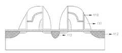
도 11은 도 10의 단위 셀(509)을 비트 라인 방향(A-A')으로 자를 경우 단면도이다. 실리콘 기판(601)위에 터널 산화막(602), 플로팅 게이트(603), 인젝션 게이트(604), 제 1 블럭 산화막(605), 제 2 블럭 산화막(606) 및 콘트롤 게이트(607)가 있다. 상기 콘트롤 게이트의 일측에 이격되어 게이트 산화막(608)과 셀렉트 게이트(609)가 있다. 상기 셀렉트 게이트의 하부 양측에 드레인 영역(611, 612)이 형성된다. 상기 콘트롤 게이트 하부 양측에 공통 소오스(610)와 드레인(612)이 위치하며, 상기 셀렉트 게이트와 상기 플로팅 게이트가 드레인 영역(612)을 함께 공유한다. 상기 드레인 영역(611)에 비트 라인 콘택(613)이 형성되며, 상기 비트 라인 콘택은 금속 비트 라인(614)에 의해 모두 하나로 연결된다.FIG. 11 is a cross-sectional view when the
도 12는 도 10의 단위 셀(509)을 워드 라인 방향(B-B')으로 자를 경우 경우의 단면도이다. 실리콘 기판 활성영역(701)위에 터널 산화막(703)과 플로팅 게이트(704), 제 1 블럭 산화막(705), 제 2 블럭 산화막(706)이 위치하며 상기 활성영역은 소자분리막(702)에 의해 분리된다. 그리고 이렇게 분리되어 있는 터널 산화막과 플로팅 게이트를 콘트롤 게이트(707)가 감싸는 구조로 되어 있다. 워드 라인 방향으로 플로팅 게이트는 각각 분리되어 있는 구조로 되어 있다.FIG. 12 is a cross-sectional view when the
상기의 공정으로 제조된 인젝션 게이트를 포함하는 비휘발성 메모리의 동작은 프로그램시 열 전자 주입이 인젝션 게이트가 위치한 터널 산화막의 영역에서 발생한다. 인젝션 게이트의 컨덕션 밴드에 전자들이 주입되며, 상기 주입된 전자들은 더 안정된 낮은 에너지 준위인 플로팅 게이트의 컨덕션 밴드로 이동한다. 따라서 프로그램시 터널 산화막은 인젝션 게이트가 위치하는 곳에 존재하는 터널 산화막이 되며, 실제 플로팅 게이트 소자의 문턱 전압을 좌우하는 터널 산화막은 플로팅 게이트가 위치하는 곳에 존재하는 터널 산화막이다. 그러므로 프로그램시 열 전자 주입에 의해 인젝션 게이트가 위치하는 곳에 존재하는 터널 산화막 또는 계면에 트랩 사이트를 발생시키더라도 플로팅 게이트 소자의 문턱 전압에는 거의 영향을 주지 않아 내구성 특성이 현저히 개선된다. 또한, 주입된 전자가 저장되어 있는 플로팅 게이트의 아래에 위치하는 터널 산화막은 열 전자 주입에 의해서는 트랩 사이트가 발생하지 않으므로 트랩 사이트에 의한 리텐션(Retention) 특성이 저하되는 문제 또한 현저히 개선된다. 또한 제 1 블럭 산화막과 제 2 블럭 산화막을 사용하여 이레이즈 후반부에 콘트롤 게이트에서 플로팅 게이트로 전자들이 MFN 터널링하여 플로팅 게이트에서 P형 기판으로 전자가 빠져나가거나 P형 기판에서 플로팅 게이트로 정공이 주입되는 것을 보상시킴으로써 이레이즈 상태의 문턱 전압을 일정한 값으로 수렴시켜 오버 이레이즈 문제를 방지함과 동시에 이레이즈 상태 문턱 전압의 분포를 좁게 만들어 오버 이레이즈에 의해 비트 라인 상의 다른 셀 데이터를 읽지 못하여 에러가 발생하는 문제와 와이드한 이레이즈 문턱 전압 분포에 의해 문턱전압 윈도우가 줄어드는 문제를 동시에 개선시킬 수 있다. 뿐만 아니라 이레이즈 문턱 전압을 일정 전압 레벨에서 좁은 폭을 가지도록 만듬으로써 프로그램 상태 문턱 전압 분포도 좁게 만들 수 있어 멀티 레벨 비트 셀의 구현을 용이하게 할 수 있다.The operation of the nonvolatile memory including the injection gate manufactured by the above process occurs when hot electron injection occurs in the region of the tunnel oxide film in which the injection gate is located during programming. Electrons are injected into the conduction band of the injection gate, and the injected electrons move into the conduction band of the floating gate, which is a more stable low energy level. Therefore, during programming, the tunnel oxide layer is a tunnel oxide layer where the injection gate is located, and the tunnel oxide layer that determines the threshold voltage of the floating gate element is a tunnel oxide layer where the floating gate is located. Therefore, even if the trap site is generated at the tunnel oxide film or the interface where the injection gate is located by hot electron injection during programming, the threshold voltage of the floating gate device is hardly influenced, and thus the durability characteristics are remarkably improved. In addition, since the trap site is not generated by the hot electron injection, the tunnel oxide film positioned below the floating gate in which the injected electrons are stored also significantly improves the problem of retention characteristics caused by the trap site. In addition, electrons are MFN tunneled from the control gate to the floating gate in the latter half of the erasure by using the first block oxide film and the second block oxide film, and electrons escape from the floating gate to the P-type substrate or holes are injected from the P-type substrate to the floating gate. By compensating for the error, the threshold voltage in the erased state is converged to a constant value to prevent the over erasure problem, and at the same time, the distribution of the erased state threshold voltage is narrowed so that other cell data on the bit line cannot be read by the over-raised error. And the problem that the threshold voltage window decreases due to the wide erase threshold voltage distribution can be improved at the same time. In addition, by making the erase threshold voltage narrow at a certain voltage level, the program state threshold voltage distribution can be narrowed, thereby facilitating the implementation of multi-level bit cells.
또한 각각의 비트 상태 즉 “00”, “01”, “10”, “11” 상태가 차지하는 문턱 전압 분포가 매우 좁아 효과적으로 에러 발생없이 리드 동작을 수행할 수 있다.In addition, since the threshold voltage distribution occupied by each bit state, that is, the states “00”, “01”, “10”, and “11” is very narrow, the read operation can be effectively performed without generating an error.
멀티 레벨 비트 노어 플래시 메모리 셀 어레이를 구현함에 있어서 셀렉트 게이트에 의해 프로그램시 선택되지 않은 셀들에 흐르는 누설 전류(Leakage Current)를 줄일 수 있어 프로그램 전류를 효과적으로 줄일 수 있어 차지 펌프(Charge Pump)회로를 그만큼 줄여 칩 사이즈를 줄일 수 있으며 이레이즈 문턱전압을 Negative로 만들 수 있어 문턱전압 윈도우를 더욱 넓게 만들 수 있다.In implementing a multi-level bit-nor-flash memory cell array, the leakage current flowing to cells not selected by the select gate can be reduced to effectively reduce the program current, thereby increasing the charge pump circuit. The chip size can be reduced, and the erase threshold voltage can be made negative, making the threshold voltage window wider.
상세히 설명된 본 발명에 의하여 본 발명의 특징부를 포함하는 변화들 및 변형들이 당해 기술 분야에서 숙련된 보통의 사람들에게 명백히 쉬워질 것임이 자명하다. 본 발명의 그러한 변형들의 범위는 본 발명의 특징부를 포함하는 당해 기술 분야에 숙련된 통상의 지식을 가진 자들의 범위 내에 있으며, 그러한 변형들은 본 발명의 청구항의 범위 내에 있는 것으로 간주된다.It will be apparent that changes and modifications incorporating features of the invention will be readily apparent to those skilled in the art by the invention described in detail. It is intended that the scope of such modifications of the invention be within the scope of those of ordinary skill in the art including the features of the invention, and such modifications are considered to be within the scope of the claims of the invention.
따라서, 본 발명의 비휘발성 메모리 소자는 플로팅 게이트는 셀프 컨버전스 이레이즈 특성을 가지는 인젝션 게이트를 구비하여 멀티 레벨 비트 노어 플래시 어레이를 효과적으로 구성하여 동작시킴으로써 다음과 같은 효과가 있다.Accordingly, in the nonvolatile memory device of the present invention, the floating gate includes an injection gate having self-convergence erase characteristics, thereby effectively configuring and operating a multi-level bit-nor flash array.
첫째, 종래의 플로팅 게이트 소자와 달리 인젝션 게이트를 사용하여 열 전자 주입이 인젝션 게이트 아래에 위치하는 터널 산화막을 통해 이루어지도록 하여 전자를 인젝션 게이트 아래에 있는 터널 산화막을 통해 인젝션 게이트의 전도대에 주입시킨 후 안정된 에너지 준위인 플로팅 게이트의 전위 우물로 흘러 들어가게 하여 열 전자 주입이되는 터널 산화막과 실제 전자들이 저장되어 소자의 문턱전압에 영향을 주는 터널 산화막을 분리시킴으로써 소자의 내구 특성과 리텐션 특성을 효과적으로 개선시킬 수 있다.First, unlike a conventional floating gate device, an injection gate is used to inject hot electrons through a tunnel oxide film positioned below the injection gate to inject electrons into the conduction band of the injection gate through the tunnel oxide film under the injection gate. It effectively improves the durability and retention characteristics of the device by separating the tunnel oxide film into which the thermal energy is injected and the tunnel oxide film which stores real electrons and flows into the potential well of the floating gate, which is a stable energy level. You can.
둘째, 종래의 플로팅 게이트 소자의 ONO대신 제 1 블럭 산화막과 제 2 블럭 산화막을 사용하여 이레이즈 동작 후반부에 콘트롤 게이트에서 플로팅 게이트로 전자들이 MFN 터널링하여 플로팅 게이트에서 P형 기판으로 전자가 빠져나가거나 P형 기판에서 플로팅 게이트로 정공이 주입되는 것을 보충시킴으로써 이레이즈 상태의 문턱 전압을 일정한 값으로 수렴시켜 오버 이레이즈 문제를 방지함과 동시에 이레이즈 상태 문턱전압의 분포를 좁게 만들어 와이드한 이레이즈 문턱 전압 분포에 의해 문턱전압 윈도우가 줄어드는 문제를 개선시킬 수 있다.Second, electrons are MFN tunneled from the control gate to the floating gate at the end of the erase operation by using the first block oxide film and the second block oxide film instead of ONO of the conventional floating gate device, and the electrons escape from the floating gate to the P-type substrate. By compensating for the injection of holes from the P-type substrate into the floating gate, the threshold voltage in the erased state is converged to a constant value to prevent the overlaid problem and the distribution of the erased threshold voltage is narrowed, thereby making the wide erase threshold The problem that the threshold voltage window is reduced by the voltage distribution can be improved.
세째 셀프 컨버전스 이레이즈 특성에 의해 각각의 비트 상태, 즉 “00”, “01”, “10”, “11” 상태가 차지하는 문턱 전압 분포를 매우 좁게 하여 효과적 으로 에러 발생없이 리드 동작을 수행할 수 있다.Third, the self-convergence erase characteristic narrows the threshold voltage distribution occupied by each bit state, namely “00”, “01”, “10”, and “11”, so that the read operation can be performed effectively without error occurrence. have.
네째 셀렉트 게이트에 의해 프로그램시 선택되지 않은 셀들에 흐르는 누설 전류를 줄일 수 있어 프로그램 전류를 효과적으로 줄일 수 있어 차지 펌프 회로를 그만큼 줄여 칩 사이즈를 줄일 수 있으며 이레이즈 문턱 전압을 Negative로 만들 수 있어 문턱전압 윈도우를 더욱 넓게 만들 수 있다.The fourth select gate reduces the leakage current flowing to cells not selected during programming, effectively reducing the program current, reducing the charge pump circuit by that much, reducing the chip size, and making the erase threshold voltage negative. You can make the window wider.
다섯째 제 1 블럭 산화막으로 사용되는 Al2O3나 Y2O3의 유전율이 각각 9와 17로 7.5정도 되는 질화막(SiN)보다 크기 때문에 ONO층을 사용하는 것 보다 제 1 블럭 산화막과 제 2 블럭 산화막을 사용하는 것이 커플링 비(Coupling Ratio)가 더 높아 콘트롤 게이트에 걸어주는 전압을 효과적으로 줄일 수 있는 효과가 있다.Fifth, since the dielectric constants of Al2 O3 and Y2 O3 used as the first block oxide film are 9 and 17, respectively, larger than the nitride film (SiN) of 7.5, respectively, the first block oxide film and the second block than the ONO layer are used. Using an oxide film has a higher coupling ratio, which effectively reduces the voltage applied to the control gate.
Claims (12)
Translated fromKoreanPriority Applications (1)
| Application Number | Priority Date | Filing Date | Title |
|---|---|---|---|
| KR1020030101092AKR100594385B1 (en) | 2003-12-31 | 2003-12-31 | Nonvolatile Memory Devices |
Applications Claiming Priority (1)
| Application Number | Priority Date | Filing Date | Title |
|---|---|---|---|
| KR1020030101092AKR100594385B1 (en) | 2003-12-31 | 2003-12-31 | Nonvolatile Memory Devices |
Publications (2)
| Publication Number | Publication Date |
|---|---|
| KR20050070813A KR20050070813A (en) | 2005-07-07 |
| KR100594385B1true KR100594385B1 (en) | 2006-06-30 |
Family
ID=37260840
Family Applications (1)
| Application Number | Title | Priority Date | Filing Date |
|---|---|---|---|
| KR1020030101092AExpired - Fee RelatedKR100594385B1 (en) | 2003-12-31 | 2003-12-31 | Nonvolatile Memory Devices |
Country Status (1)
| Country | Link |
|---|---|
| KR (1) | KR100594385B1 (en) |
Families Citing this family (1)
| Publication number | Priority date | Publication date | Assignee | Title |
|---|---|---|---|---|
| KR101580172B1 (en)* | 2009-07-03 | 2015-12-28 | 주식회사 동부하이텍 | Fabricating method of embedded flash memory device |
- 2003
- 2003-12-31KRKR1020030101092Apatent/KR100594385B1/ennot_activeExpired - Fee Related
Also Published As
| Publication number | Publication date |
|---|---|
| KR20050070813A (en) | 2005-07-07 |
Similar Documents
| Publication | Publication Date | Title |
|---|---|---|
| US5471422A (en) | EEPROM cell with isolation transistor and methods for making and operating the same | |
| US7046552B2 (en) | Flash memory with enhanced program and erase coupling and process of fabricating the same | |
| US6426896B1 (en) | Flash memory cell with contactless bit line, and process of fabrication | |
| US5824584A (en) | Method of making and accessing split gate memory device | |
| US7804121B2 (en) | Flash memory device and programming and erasing methods therewith | |
| US6844588B2 (en) | Non-volatile memory | |
| US20040057286A1 (en) | Self-aligned split-gate NAND flash memory and fabrication process | |
| US20060068529A1 (en) | Self-aligned split-gate NAND flash memory and fabrication process | |
| US6580630B1 (en) | Initialization method of P-type silicon nitride read only memory | |
| WO2005048269A2 (en) | Flash memory programming using gate induced junction leakage current | |
| US7439574B2 (en) | Silicon/oxide/nitride/silicon nonvolatile memory with vertical channels | |
| US6313498B1 (en) | Flash memory cell with thin floating gate with rounded side wall, and fabrication process | |
| US20080293200A1 (en) | Method of fabricating nonvolatile semiconductor memory device | |
| KR100601915B1 (en) | Nonvolatile Memory Devices | |
| KR100609216B1 (en) | Nonvolatile Memory Devices | |
| KR100594385B1 (en) | Nonvolatile Memory Devices | |
| KR100594384B1 (en) | Nonvolatile Memory Devices | |
| KR100657151B1 (en) | Nonvolatile Memory Device and Manufacturing Method Thereof | |
| KR100604989B1 (en) | Nonvolatile Memory Device and Manufacturing Method Thereof | |
| US7510936B2 (en) | Nonvolatile memory device and methods of fabricating and driving the same | |
| US20240355396A1 (en) | Flash memory cell, writing method and erasing method therefor | |
| KR100591122B1 (en) | Flash memory, its driving method and arrangement thereof | |
| KR100609237B1 (en) | Nonvolatile Memory Devices | |
| KR100567350B1 (en) | Method for fabricating non-volatile memory device | |
| KR20060000790A (en) | Manufacturing Method of Flash Memory Device |
Legal Events
| Date | Code | Title | Description |
|---|---|---|---|
| A201 | Request for examination | ||
| PA0109 | Patent application | St.27 status event code:A-0-1-A10-A12-nap-PA0109 | |
| PA0201 | Request for examination | St.27 status event code:A-1-2-D10-D11-exm-PA0201 | |
| R18-X000 | Changes to party contact information recorded | St.27 status event code:A-3-3-R10-R18-oth-X000 | |
| PG1501 | Laying open of application | St.27 status event code:A-1-1-Q10-Q12-nap-PG1501 | |
| D13-X000 | Search requested | St.27 status event code:A-1-2-D10-D13-srh-X000 | |
| D14-X000 | Search report completed | St.27 status event code:A-1-2-D10-D14-srh-X000 | |
| E902 | Notification of reason for refusal | ||
| PE0902 | Notice of grounds for rejection | St.27 status event code:A-1-2-D10-D21-exm-PE0902 | |
| E13-X000 | Pre-grant limitation requested | St.27 status event code:A-2-3-E10-E13-lim-X000 | |
| P11-X000 | Amendment of application requested | St.27 status event code:A-2-2-P10-P11-nap-X000 | |
| P13-X000 | Application amended | St.27 status event code:A-2-2-P10-P13-nap-X000 | |
| E701 | Decision to grant or registration of patent right | ||
| PE0701 | Decision of registration | St.27 status event code:A-1-2-D10-D22-exm-PE0701 | |
| PN2301 | Change of applicant | St.27 status event code:A-3-3-R10-R13-asn-PN2301 St.27 status event code:A-3-3-R10-R11-asn-PN2301 | |
| PN2301 | Change of applicant | St.27 status event code:A-3-3-R10-R13-asn-PN2301 St.27 status event code:A-3-3-R10-R11-asn-PN2301 | |
| GRNT | Written decision to grant | ||
| PR0701 | Registration of establishment | St.27 status event code:A-2-4-F10-F11-exm-PR0701 | |
| PR1002 | Payment of registration fee | St.27 status event code:A-2-2-U10-U11-oth-PR1002 Fee payment year number:1 | |
| PG1601 | Publication of registration | St.27 status event code:A-4-4-Q10-Q13-nap-PG1601 | |
| PR1001 | Payment of annual fee | St.27 status event code:A-4-4-U10-U11-oth-PR1001 Fee payment year number:4 | |
| PR1001 | Payment of annual fee | St.27 status event code:A-4-4-U10-U11-oth-PR1001 Fee payment year number:5 | |
| PR1001 | Payment of annual fee | St.27 status event code:A-4-4-U10-U11-oth-PR1001 Fee payment year number:6 | |
| FPAY | Annual fee payment | Payment date:20120521 Year of fee payment:7 | |
| PR1001 | Payment of annual fee | St.27 status event code:A-4-4-U10-U11-oth-PR1001 Fee payment year number:7 | |
| LAPS | Lapse due to unpaid annual fee | ||
| PC1903 | Unpaid annual fee | St.27 status event code:A-4-4-U10-U13-oth-PC1903 Not in force date:20130622 Payment event data comment text:Termination Category : DEFAULT_OF_REGISTRATION_FEE | |
| PC1903 | Unpaid annual fee | St.27 status event code:N-4-6-H10-H13-oth-PC1903 Ip right cessation event data comment text:Termination Category : DEFAULT_OF_REGISTRATION_FEE Not in force date:20130622 | |
| P22-X000 | Classification modified | St.27 status event code:A-4-4-P10-P22-nap-X000 | |
| P22-X000 | Classification modified | St.27 status event code:A-4-4-P10-P22-nap-X000 | |
| P22-X000 | Classification modified | St.27 status event code:A-4-4-P10-P22-nap-X000 | |
| P22-X000 | Classification modified | St.27 status event code:A-4-4-P10-P22-nap-X000 |