KR100594242B1 - Source driver and source line driving method for driving flat panel display - Google Patents
Source driver and source line driving method for driving flat panel displayDownload PDFInfo
- Publication number
- KR100594242B1 KR100594242B1KR1020040005650AKR20040005650AKR100594242B1KR 100594242 B1KR100594242 B1KR 100594242B1KR 1020040005650 AKR1020040005650 AKR 1020040005650AKR 20040005650 AKR20040005650 AKR 20040005650AKR 100594242 B1KR100594242 B1KR 100594242B1
- Authority
- KR
- South Korea
- Prior art keywords
- precharge
- signal
- color
- signals
- digital
- Prior art date
- Legal status (The legal status is an assumption and is not a legal conclusion. Google has not performed a legal analysis and makes no representation as to the accuracy of the status listed.)
- Expired - Fee Related
Links
Images


Classifications
- A—HUMAN NECESSITIES
- A47—FURNITURE; DOMESTIC ARTICLES OR APPLIANCES; COFFEE MILLS; SPICE MILLS; SUCTION CLEANERS IN GENERAL
- A47J—KITCHEN EQUIPMENT; COFFEE MILLS; SPICE MILLS; APPARATUS FOR MAKING BEVERAGES
- A47J36/00—Parts, details or accessories of cooking-vessels
- A47J36/06—Lids or covers for cooking-vessels
- A47J36/08—Lids or covers for cooking-vessels for draining liquids from vessels
- G—PHYSICS
- G09—EDUCATION; CRYPTOGRAPHY; DISPLAY; ADVERTISING; SEALS
- G09G—ARRANGEMENTS OR CIRCUITS FOR CONTROL OF INDICATING DEVICES USING STATIC MEANS TO PRESENT VARIABLE INFORMATION
- G09G3/00—Control arrangements or circuits, of interest only in connection with visual indicators other than cathode-ray tubes
- G09G3/20—Control arrangements or circuits, of interest only in connection with visual indicators other than cathode-ray tubes for presentation of an assembly of a number of characters, e.g. a page, by composing the assembly by combination of individual elements arranged in a matrix no fixed position being assigned to or needed to be assigned to the individual characters or partial characters
- A—HUMAN NECESSITIES
- A47—FURNITURE; DOMESTIC ARTICLES OR APPLIANCES; COFFEE MILLS; SPICE MILLS; SUCTION CLEANERS IN GENERAL
- A47J—KITCHEN EQUIPMENT; COFFEE MILLS; SPICE MILLS; APPARATUS FOR MAKING BEVERAGES
- A47J27/00—Cooking-vessels
- A47J27/002—Construction of cooking-vessels; Methods or processes of manufacturing specially adapted for cooking-vessels
- G—PHYSICS
- G09—EDUCATION; CRYPTOGRAPHY; DISPLAY; ADVERTISING; SEALS
- G09G—ARRANGEMENTS OR CIRCUITS FOR CONTROL OF INDICATING DEVICES USING STATIC MEANS TO PRESENT VARIABLE INFORMATION
- G09G2300/00—Aspects of the constitution of display devices
- G09G2300/04—Structural and physical details of display devices
- G09G2300/0439—Pixel structures
- G09G2300/0443—Pixel structures with several sub-pixels for the same colour in a pixel, not specifically used to display gradations
- G—PHYSICS
- G09—EDUCATION; CRYPTOGRAPHY; DISPLAY; ADVERTISING; SEALS
- G09G—ARRANGEMENTS OR CIRCUITS FOR CONTROL OF INDICATING DEVICES USING STATIC MEANS TO PRESENT VARIABLE INFORMATION
- G09G2310/00—Command of the display device
- G09G2310/02—Addressing, scanning or driving the display screen or processing steps related thereto
- G09G2310/0243—Details of the generation of driving signals
- G09G2310/0248—Precharge or discharge of column electrodes before or after applying exact column voltages
- G—PHYSICS
- G09—EDUCATION; CRYPTOGRAPHY; DISPLAY; ADVERTISING; SEALS
- G09G—ARRANGEMENTS OR CIRCUITS FOR CONTROL OF INDICATING DEVICES USING STATIC MEANS TO PRESENT VARIABLE INFORMATION
- G09G2310/00—Command of the display device
- G09G2310/02—Addressing, scanning or driving the display screen or processing steps related thereto
- G09G2310/0264—Details of driving circuits
- G09G2310/027—Details of drivers for data electrodes, the drivers handling digital grey scale data, e.g. use of D/A converters
- G—PHYSICS
- G09—EDUCATION; CRYPTOGRAPHY; DISPLAY; ADVERTISING; SEALS
- G09G—ARRANGEMENTS OR CIRCUITS FOR CONTROL OF INDICATING DEVICES USING STATIC MEANS TO PRESENT VARIABLE INFORMATION
- G09G2320/00—Control of display operating conditions
- G09G2320/02—Improving the quality of display appearance
- G09G2320/0242—Compensation of deficiencies in the appearance of colours
- G—PHYSICS
- G09—EDUCATION; CRYPTOGRAPHY; DISPLAY; ADVERTISING; SEALS
- G09G—ARRANGEMENTS OR CIRCUITS FOR CONTROL OF INDICATING DEVICES USING STATIC MEANS TO PRESENT VARIABLE INFORMATION
- G09G3/00—Control arrangements or circuits, of interest only in connection with visual indicators other than cathode-ray tubes
- G09G3/20—Control arrangements or circuits, of interest only in connection with visual indicators other than cathode-ray tubes for presentation of an assembly of a number of characters, e.g. a page, by composing the assembly by combination of individual elements arranged in a matrix no fixed position being assigned to or needed to be assigned to the individual characters or partial characters
- G09G3/34—Control arrangements or circuits, of interest only in connection with visual indicators other than cathode-ray tubes for presentation of an assembly of a number of characters, e.g. a page, by composing the assembly by combination of individual elements arranged in a matrix no fixed position being assigned to or needed to be assigned to the individual characters or partial characters by control of light from an independent source
- G09G3/36—Control arrangements or circuits, of interest only in connection with visual indicators other than cathode-ray tubes for presentation of an assembly of a number of characters, e.g. a page, by composing the assembly by combination of individual elements arranged in a matrix no fixed position being assigned to or needed to be assigned to the individual characters or partial characters by control of light from an independent source using liquid crystals
- G09G3/3611—Control of matrices with row and column drivers
- G09G3/3614—Control of polarity reversal in general
- G—PHYSICS
- G09—EDUCATION; CRYPTOGRAPHY; DISPLAY; ADVERTISING; SEALS
- G09G—ARRANGEMENTS OR CIRCUITS FOR CONTROL OF INDICATING DEVICES USING STATIC MEANS TO PRESENT VARIABLE INFORMATION
- G09G3/00—Control arrangements or circuits, of interest only in connection with visual indicators other than cathode-ray tubes
- G09G3/20—Control arrangements or circuits, of interest only in connection with visual indicators other than cathode-ray tubes for presentation of an assembly of a number of characters, e.g. a page, by composing the assembly by combination of individual elements arranged in a matrix no fixed position being assigned to or needed to be assigned to the individual characters or partial characters
- G09G3/34—Control arrangements or circuits, of interest only in connection with visual indicators other than cathode-ray tubes for presentation of an assembly of a number of characters, e.g. a page, by composing the assembly by combination of individual elements arranged in a matrix no fixed position being assigned to or needed to be assigned to the individual characters or partial characters by control of light from an independent source
- G09G3/36—Control arrangements or circuits, of interest only in connection with visual indicators other than cathode-ray tubes for presentation of an assembly of a number of characters, e.g. a page, by composing the assembly by combination of individual elements arranged in a matrix no fixed position being assigned to or needed to be assigned to the individual characters or partial characters by control of light from an independent source using liquid crystals
- G09G3/3611—Control of matrices with row and column drivers
- G09G3/3685—Details of drivers for data electrodes
- G09G3/3688—Details of drivers for data electrodes suitable for active matrices only
- Y—GENERAL TAGGING OF NEW TECHNOLOGICAL DEVELOPMENTS; GENERAL TAGGING OF CROSS-SECTIONAL TECHNOLOGIES SPANNING OVER SEVERAL SECTIONS OF THE IPC; TECHNICAL SUBJECTS COVERED BY FORMER USPC CROSS-REFERENCE ART COLLECTIONS [XRACs] AND DIGESTS
- Y10—TECHNICAL SUBJECTS COVERED BY FORMER USPC
- Y10S—TECHNICAL SUBJECTS COVERED BY FORMER USPC CROSS-REFERENCE ART COLLECTIONS [XRACs] AND DIGESTS
- Y10S220/00—Receptacles
- Y10S220/912—Cookware, i.e. pots and pans
Landscapes
- Engineering & Computer Science (AREA)
- Physics & Mathematics (AREA)
- Computer Hardware Design (AREA)
- General Physics & Mathematics (AREA)
- Theoretical Computer Science (AREA)
- Food Science & Technology (AREA)
- Control Of Indicators Other Than Cathode Ray Tubes (AREA)
- Liquid Crystal Display Device Control (AREA)
Abstract
Translated fromKoreanDescription
Translated fromKorean본 발명의 상세한 설명에서 인용되는 도면을 보다 충분히 이해하기 위하여 각 도면의 간단한 설명이 제공된다.BRIEF DESCRIPTION OF THE DRAWINGS In order to better understand the drawings cited in the detailed description of the invention, a brief description of each drawing is provided.
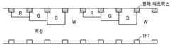
도 1은 일반적인 TFT-LCD 패널과 주변 회로를 나타내는 블록도이다.1 is a block diagram showing a general TFT-LCD panel and a peripheral circuit.
도 2는 일반적인 픽셀 구조를 나타내는 도면이다.2 is a diagram illustrating a general pixel structure.
도 3은 종래의 소스 드라이버를 나타내는 블록도이다.3 is a block diagram showing a conventional source driver.
도 4a 내지 도 4c는 개발이 시도되고있는 픽셀 구조들을 나타내는 도면이다.4A-4C are diagrams illustrating pixel structures in which development is being attempted.
도 5는 일반적인 TFT-LCD 패널의 상판과 하판을 나타내는 도면이다.5 is a diagram illustrating a top plate and a bottom plate of a general TFT-LCD panel.
도 6은 본 발명의 일실시예에 따른 소스 드라이버를 나타내는 블록도이다.6 is a block diagram illustrating a source driver according to an embodiment of the present invention.
도 7은 본 발명의 다른 실시예에 따른 소스드라이버를 나타내는 블록도이다.7 is a block diagram illustrating a source driver according to another exemplary embodiment of the present invention.
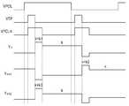
도 8은 도 7의 소스 드라이버의 동작 설명을 위한 타이밍도이다.FIG. 8 is a timing diagram for describing an operation of the source driver of FIG. 7.
도 9는 본발명의 또다른 실시예에따른 소스드라이버를 나타내는 블록도이다.9 is a block diagram showing a source driver according to another embodiment of the present invention.
도 10은 도 9의 소스 드라이버의 동작 설명을 위한 타이밍도이다.10 is a timing diagram for describing an operation of a source driver of FIG. 9.
본 발명은 평판 표시 장치에 관한 것으로, 특히 평판 표시 장치의 소오스 라인을 구동하는 소스 드라이버에 관한 것이다.The present invention relates to a flat panel display, and more particularly to a source driver for driving a source line of the flat panel display.
평판 표시 장치들(flat panel displays) 중 대표적인 것은 박막 트랜지스터(thin film transistor:TFT)-액정 표시 장치(liquid crystal display)(LCD) 방식으로 디스플레이한다. 이외에도, 평판 표시 장치에는 유기 EL(electro luminance) 방식, STN(super twisted nematic)-LCD 방식, PDP(plasma display panel) 방식 등이 사용되고 있다.Representative of flat panel displays is a thin film transistor (TFT) -liquid crystal display (LCD) method. In addition, an organic electroluminescence (EL) method, a super twisted nematic (STN) -LCD method, a plasma display panel (PDP) method, or the like is used for the flat panel display device.
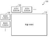
이하, TFT-LCD는 현재 가장 널리 사용되고 있는 평판 표시장치들(flat panel displays) 중의 하나이므로, 이를 중심으로 설명한다. 도 1은 일반적인 TFT-LCD 패널과 주변 회로를 나타내는 블록도이다. LCD 패널(110)은 전계를 형성하기 위한 다수의 전극들을 구비하는 상판과 하판으로 구성되고(도 5참조), 상판과 하판 사이에는 액정층으로 이루어져 있으며, 이외에도 빛을 편광(polarizing)시키기 위하여 상판과 하판에 부착되는 편광판을 구비한다. TFT-LCD(100)에서 빛의 밝기는 액정 분자를 재배열시키기 위한 전극에 계조에 따른 전압을 인가함으로써 조절된다. LCD 패널의 하판에는 계조 전압이 전극에 인가되도록 스위칭하기 위하여, 전극에 연결된 박막 트랜지스터(TFT)와 같은 다수의 스위칭 소자들이 구비되어 있다. TFT와 같은 스위칭 소자들에 의하여 픽셀 단위로 빛의 밝기가 조절되고, 도 2와 같이 배열되는 컬러 필터 배열을 가지는 픽셀 구조에 의하여 3 색, R(red), G(green), B(blue)가 표시된다.Hereinafter, since the TFT-LCD is one of the flat panel displays that are most widely used at present, it will be mainly described. 1 is a block diagram showing a general TFT-LCD panel and a peripheral circuit. The
TFT-LCD(100)는 LCD 패널(110)에 가로로 구비된 다수의 게이트 라인을 구동 하기 위한 게이트 드라이버들(120)과 LCD 패널(110)에 세로로 구비된 다수의 소스 라인을 구동하기 위한 소스 드라이버들(130)로 이루어진 구동 회로부와 스위칭 소자들을 통하여 전극에 계조 전압(grey voltage)을 공급하기 위하여 상기 구동 회로부를 콘트롤하는 콘트롤러부(미도시)를 구비한다. 일반적으로, 상기 콘트롤러부(미도시)는 상기 LCD 패널(110) 외부에 배치된다. 상기 구동 회로부는 일반적으로 LCD 패널(110) 외부에 배치되지만, COG(chip on glass) 타입의 경우 LCD 패널(110) 상에 배치될 수 있다.The TFT-
도 3은 종래의 소스 드라이버(130)를 나타내는 블록도이다. 도 3을 참조하면, 종래의 소스 드라이버(130)는 버퍼(131), 및 디지털-아날로그 변환기(DAC:digital-analog converter)(132)를 구비한다. 디지털-아날로그 변환기(132)는 외부의 콘트롤러부(미도시)에서 입력되는 일정 계조 값(grey value)을 가지는 R, G, 또는 B 디지털 데이터를 해당 계조 전압의 아날로그 신호로 변환하여 출력한다. 디지털-아날로그 변환기(132)에서 출력되는 아날로그 영상신호는 버퍼(131)에서 버퍼링되어 소스 라인으로 출력된다. 버퍼(131)는 다수의 MOSFET(metal-oxide-semiconductor field effect transistor)으로 이루어진 오피 앰프(operational amplifier) 형태의 아날로그 회로이며, 이와 같은 오피 앰프는 일정 바이어스 전압(BIAS)을 이용하여 입력되는 영상신호의 전류 구동 능력을 향상시킨다. 전류 구동 능력이 향상된 형태로 버퍼(131)에서 출력되는 영상신호는 LCD 패널(110) 상의 소스 라인과 해당 픽셀을 빠르게 충전시킨다. 영상신호를 전달받은 픽셀은 해당 계조 전압(grey voltage)에 비례하도록 액정 분자를 재배열시킴에 따 라 빛의 밝기가 조절된다.3 is a block diagram illustrating a
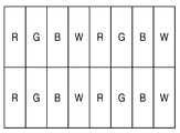
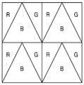
도 4a 내지 도 4c는 개발이 시도되고 있는 픽셀 구조들을 나타내는 도면이다. LCD 패널(110)의 대형화 및 고해상도화가 진행되면서 휘도 향상의 목적을 두고 화이트(white) 픽셀을 추가하여, 도 4a와 같은 R, G, B, W 픽셀 구조가 제안되었다. 사람의 원추 세포 비율에 따른 색상별 인지능력의 차이를 감안하여, 최근에는 도 4b 또는 도 4c와 같이 특정 컬러를 강조한 다양한 픽셀 구조가 제안되고 있다. 이와 같이, 픽셀 구조가 달라지면서 픽셀간 면적이 달라지고, 이와 함께 도 5와 같이 픽셀간 컬러 필터를 형성하는 물질인 PR(photo resist)의 픽셀간 두께 차이 등으로 인하여, 픽셀마다 부하(load)가 달라진다. PR의 픽셀간 두께 차이는 도 2와 같은 일반적인 픽셀 구조에서도 나타난다. 소스 드라이버(130)에 의하여 픽셀에 영상신호가 충전될 때, 픽셀마다 부하가 다르면, 같은 계조 전압을 가지는 색 신호의 충전 특성이 달라지므로, 같은 밝기를 나타내어야 할 픽셀들이 서로 다른 색재현성을 가지는 문제점이 있다.4A-4C are diagrams illustrating pixel structures in which development is being attempted. As the
따라서, 본 발명이 이루고자 하는 기술적인 과제는, 서로 다른 부하를 가지는 R, G, B 픽셀들 각각에서 같은 충전 특성이 나타나도록 하기 위하여, 색 신호 R, G, B 각각을 전달하는 출력 핀간 구동 능력이 다르게 조절될 수 있는 평판 표시 장치 구동을 위한 소스 드라이버를 제공하는 데 있다.Therefore, the technical problem to be achieved by the present invention is to drive the output pin-to-pin output of each of the color signals R, G, B, so that the same charging characteristics appear in each of the R, G, B pixels having different loads The present invention provides a source driver for driving a flat panel display device which can be adjusted differently.
본 발명이 이루고자 하는 다른 기술적인 과제는, 서로 다른 부하를 가지는 R, G, B 픽셀들 각각에서 같은 충전 특성이 나타나도록 하기 위한 평판 표시 장치 의 소스라인을 구동하는 방법을 제공하는 데 있다.Another object of the present invention is to provide a method of driving a source line of a flat panel display device such that the same charging characteristic is displayed in each of R, G, and B pixels having different loads.
상기의 기술적 과제를 달성하기 위한 본 발명의 일면에 따른 평판 표시 장치 구동을 위한 소스 드라이버는, 디지털-아날로그 변환기들, 제1 버퍼, 제2 버퍼, 제3 버퍼를 구비하는 것을 특징으로 한다. 상기 디지털-아날로그 변환기들은 계조값에 따라 변하는 디지털의 제1, 제2, 및 제3 색 신호들 각각을 아날로그 영상신호로 변환하여 출력한다. 상기 제1 버퍼는 제1 바이어스 전압을 이용하여 상기 제1 색 신호가 변환된 아날로그 영상신호를 버퍼링하여 출력한다. 상기 제2 버퍼는 제2 바이어스 전압을 이용하여 상기 제2 색 신호가 변환된 아날로그 영상신호를 버퍼링하여 출력한다. 상기 제3 버퍼는 제3 바이어스 전압을 이용하여 상기 제3 색 신호가 변환된 아날로그 영상신호를 버퍼링하여 출력한다.According to an aspect of the present invention, a source driver for driving a flat panel display device includes digital-to-analog converters, a first buffer, a second buffer, and a third buffer. The digital-to-analog converters convert digital first, second, and third color signals that vary according to grayscale values, into analog video signals and output the analog video signals. The first buffer buffers and outputs an analog video signal obtained by converting the first color signal using a first bias voltage. The second buffer buffers and outputs an analog video signal obtained by converting the second color signal using a second bias voltage. The third buffer buffers and outputs an analog video signal obtained by converting the third color signal using a third bias voltage.
상기의 기술적 과제를 달성하기 위한 본 발명의 다른 일면에 따른 평판 표시 장치 구동을 위한 소스 드라이버는, 프리차지 콘트롤 회로들, 레벨 쉬프터들, 디지털-아날로그 변환기들, 및 버퍼들을 구비하는 것을 특징으로 한다. 상기 프리차지 콘트롤 회로들은 계조값에 따라 변하는 디지털의 제1, 제2, 및 제3 색 신호들 각각에, 소정 펄스폭들을 가지는 제1, 제2, 및 제3 프리차지 신호를 합하여, 상기 소정 펄스폭 동안만큼 상기 제1, 제2, 및 제3 색 신호들 각각을 프리차지 계조값으로 유지시킨다. 상기 레벨 쉬프터들은 상기 프리차지 계조값이 합해진 제1, 제2, 및 제3 색 신호들 각각의 전압 크기를 일정 레벨로 상승시킨다. 상기 디지털-아날로그 변환기들은 상기 레벨 상승된 제1, 제2, 및 제3 색 신호들 각각을 아날로그 영상신호 로 변환하여 출력한다. 상기 버퍼들은 상기 레벨 상승된 제1, 제2, 및 제3 색 신호들 각각이 변환된 아날로그 영상신호를 버퍼링하여 출력한다.According to another aspect of the present invention, a source driver for driving a flat panel display device includes precharge control circuits, level shifters, digital-to-analog converters, and buffers. . The precharge control circuits add the first, second, and third precharge signals having predetermined pulse widths to each of the digital first, second, and third color signals that vary according to the grayscale value, and the predetermined value. Each of the first, second, and third color signals is maintained at the precharge gray value for the pulse width. The level shifters increase a voltage level of each of the first, second, and third color signals in which the precharge gray value is added to a predetermined level. The digital-to-analog converters convert each of the first, second, and third color signals of the level up into an analog image signal and output the analog image signal. The buffers buffer and output analog video signals obtained by converting each of the first, second, and third color signals having the increased levels.
상기의 기술적 과제를 달성하기 위한 본 발명의 또 다른 일면에 따른 평판 표시 장치 구동을 위한 소스 드라이버는, 제1 프리차지 콘트롤 회로, 제2 프리차지 콘트롤 회로, 제3 프리차지 콘트롤 회로, 레벨 쉬프터들, 디지털-아날로그 변환기들, 및 버퍼들을 구비하는 것을 특징으로 한다. 상기 제1 프리차지 콘트롤 회로는 프리차지 제어 신호를 이용하여 제1 프리차지 신호를 생성하고, 계조값에 따라 변하는 디지털의 제1 색 신호에 상기 제1 프리차지 신호를 합하여, 상기 제1 색 신호를 소정 펄스폭 동안만큼 제1 프리차지 계조값으로 유지시킨다. 상기 제2 프리차지 콘트롤 회로는 상기 프리차지 제어 신호를 이용하여 제2 프리차지 신호를 생성하고, 계조값에 따라 변하는 디지털의 제2 색 신호에 상기 제2 프리차지 신호를 합하여, 상기 제2 색 신호를 상기 소정 펄스폭 동안만큼 제2 프리차지 계조값으로 유지시킨다. 상기 제3 프리차지 콘트롤 회로는 상기 프리차지 제어 신호를 이용하여 제3 프리차지 신호를 생성하고, 계조값에 따라 변하는 디지털의 제3 색 신호에 상기 제3 프리차지 신호를 합하여, 상기 제3 색 신호를 상기 소정 펄스폭 동안만큼 제3 프리차지 계조값으로 유지시킨다. 상기 레벨 쉬프터들은 상기 프리차지 계조값들이 합해진 제1, 제2, 및 제3 색 신호들 각각의 전압 크기를 일정 레벨로 상승시킨다. 상기 디지털-아날로그 변환기들은 상기 레벨 상승된 제1, 제2, 및 제3 색 신호들 각각을 아날로그 영상신호로 변환하여 출력한다. 상기 버퍼들은 상기 레벨 상승된 제1, 제2, 및 제3 색 신호들 각각이 변환된 아날로그 영상신호를 버퍼링하여 출력한다.According to another aspect of the present invention, a source driver for driving a flat panel display device includes a first precharge control circuit, a second precharge control circuit, a third precharge control circuit, and level shifters. , Digital-to-analog converters, and buffers. The first precharge control circuit generates a first precharge signal using a precharge control signal, adds the first precharge signal to a digital first color signal that changes according to a gray value, and then adds the first precharge signal to the first color signal. Is maintained at the first precharge gray value for a predetermined pulse width. The second precharge control circuit generates a second precharge signal using the precharge control signal, adds the second precharge signal to a digital second color signal that changes according to the gray scale value, and adds the second precharge signal. The signal is held at the second precharge gray value for the predetermined pulse width. The third precharge control circuit generates a third precharge signal using the precharge control signal, adds the third precharge signal to a digital third color signal that changes according to a gray value, and then adds the third precharge signal. The signal is held at the third precharge gray value for the predetermined pulse width. The level shifters increase a voltage level of each of the first, second, and third color signals in which the precharge gray values are summed to a predetermined level. The digital-to-analog converters convert each of the first, second, and third color signals of the level up into an analog image signal and output the analog image signal. The buffers buffer and output analog video signals obtained by converting each of the first, second, and third color signals having the increased levels.
상기의 다른 기술적 과제를 달성하기 위한 본 발명의 일면에 따른 평판 표시 장치 구동을 위한 소스라인 구동 방법은, 계조값에 따라 변하는 디지털의 제1, 제2, 및 제3 색 신호들 각각을 아날로그 영상신호로 변환하여 출력하는 단계; 제1 바이어스 전압을 이용하여 상기 제1 색 신호가 변환된 아날로그 영상신호를 버퍼링하여 출력하는 단계; 제2 바이어스 전압을 이용하여 상기 제2 색 신호가 변환된 아날로그 영상신호를 버퍼링하여 출력하는 단계; 및 제3 바이어스 전압을 이용하여 상기 제3 색 신호가 변환된 아날로그 영상신호를 버퍼링하여 출력하는 단계를 구비하는 것을 특징으로 한다.According to another aspect of the present invention, there is provided a source line driving method for driving a flat panel display device, wherein each of digital first, second, and third color signals that vary according to grayscale values is converted into an analog image. Converting and outputting the signal; Buffering and outputting an analog video signal converted from the first color signal using a first bias voltage; Buffering and outputting an analog video signal converted from the second color signal using a second bias voltage; And buffering and outputting an analog video signal converted from the third color signal by using a third bias voltage.
상기의 다른 기술적 과제를 달성하기 위한 본 발명의 다른 일면에 따른 평판 표시 장치 구동을 위한 소스라인 구동 방법은, 계조값에 따라 변하는 디지털의 제1, 제2, 및 제3 색 신호들 각각에, 소정 펄스폭들을 가지는 제1, 제2, 및 제3 프리차지 신호를 합하여, 상기 소정 펄스폭 동안만큼 상기 제1, 제2, 및 제3 색 신호들 각각을 프리차지 계조값으로 유지시켜 출력하는 단계; 상기 프리차지 계조값이 합해진 제1, 제2, 및 제3 색 신호들 각각의 전압 크기를 일정 레벨로 상승시키는 단계; 상기 레벨 상승된 제1, 제2, 및 제3 색 신호들 각각을 아날로그 영상신호로 변환하여 출력하는 단계; 및 상기 레벨 상승된 제1, 제2, 및 제3 색 신호들 각각이 변환된 아날로그 영상신호를 버퍼링하여 출력하는 단계를 구비하는 것을 특징으로 한다.According to another aspect of the present invention, there is provided a source line driving method for driving a flat panel display device, the digital first, second, and third color signals varying according to grayscale values. The first, second, and third precharge signals having predetermined pulse widths are summed, and each of the first, second, and third color signals is maintained at a precharge gray value for the predetermined pulse width and output. step; Increasing a voltage level of each of the first, second, and third color signals in which the precharge gray value is added to a predetermined level; Converting each of the level-up first, second, and third color signals into an analog video signal and outputting the analog video signal; And buffering and outputting the analog video signal converted from each of the level-up first, second, and third color signals.
상기의 다른 기술적 과제를 달성하기 위한 본 발명의 또 다른 일면에 따른 평판 표시 장치 구동을 위한 소스라인 구동 방법은, 프리차지 제어 신호를 이용하여 제1 프리차지 신호를 생성하고, 계조값에 따라 변하는 디지털의 제1 색 신호에 상기 제1 프리차지 신호를 소정 펄스폭 동안만큼 합하여, 상기 제1 색 신호를 제1 프리차지 계조값으로 유지시켜 출력하는 단계; 상기 프리차지 제어 신호를 이용하여 제2 프리차지 신호를 생성하고, 계조값에 따라 변하는 디지털의 제2 색 신호에 상기 제2 프리차지 신호를 상기 소정 펄스폭 동안만큼 합하여, 상기 제2 색 신호를 제2 프리차지 계조값으로 유지시켜 출력하는 단계; 상기 프리차지 제어 신호를 이용하여 제3 프리차지 신호를 생성하고, 계조값에 따라 변하는 디지털의 제3 색 신호에 상기 제3 프리차지 신호를 상기 소정 펄스폭 동안만큼 합하여, 상기 제3 색 신호를 제3 프리차지 계조값으로 유지시켜 출력하는 단계; 상기 프리차지 계조값들이 합해진 제1, 제2, 및 제3 색 신호들 각각의 전압 크기를 일정 레벨로 상승시키는 단계; 상기 레벨 상승된 제1, 제2, 및 제3 색 신호들 각각을 아날로그 영상신호로 변환하여 출력하는 단계; 및 상기 레벨 상승된 제1, 제2, 및 제3 색 신호들 각각이 변환된 아날로그 영상신호를 버퍼링하여 출력하는 단계를 구비하는 것을 특징으로 한다.In accordance with another aspect of the present invention, a source line driving method for driving a flat panel display may generate a first precharge signal using a precharge control signal, and may vary according to a gray value. Adding the first precharge signal to a digital first color signal by a predetermined pulse width to maintain the first color signal at a first precharge gray value and output the first color signal; A second precharge signal is generated by using the precharge control signal, and the second precharge signal is added to the digital second color signal which varies according to the gray scale value by the predetermined pulse width for the second color signal. Maintaining and outputting the second precharge gray value; The third precharge signal is generated using the precharge control signal, and the third precharge signal is added to the digital third color signal which changes according to the gray scale value for the predetermined pulse width, thereby generating the third color signal. Maintaining and outputting the third precharge gray value; Increasing a voltage level of each of the first, second, and third color signals in which the precharge gray values are summed to a predetermined level; Converting each of the level-up first, second, and third color signals into an analog video signal and outputting the analog video signal; And buffering and outputting the analog video signal converted from each of the level-up first, second, and third color signals.
본 발명과 본 발명의 동작상의 이점 및 본 발명의 실시에 의하여 달성되는 목적을 충분히 이해하기 위해서는 본 발명의 바람직한 실시예를 예시하는 첨부 도면 및 첨부 도면에 기재된 내용을 참조하여야만 한다.In order to fully understand the present invention, the operational advantages of the present invention, and the objects achieved by the practice of the present invention, reference should be made to the accompanying drawings which illustrate preferred embodiments of the present invention and the contents described in the accompanying drawings.
이하, 첨부한 도면을 참조하여 본 발명의 바람직한 실시예를 설명함으로써, 본 발명을 상세히 설명한다. 각 도면에 제시된 동일한 참조부호는 동일한 부재를 나타낸다.Hereinafter, exemplary embodiments of the present invention will be described in detail with reference to the accompanying drawings. Like reference numerals in the drawings denote like elements.
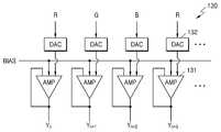
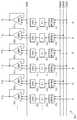
도 6은 본 발명의 일실시예에 따른 소스 드라이버(600)를 나타내는 블록도이다. 도 6을 참조하면, 본 발명의 일실시예에 따른 소스 드라이버(600)는 다수개의 디지털-아날로그 변환기들(611, 621, 631), 및 다수개의 버퍼들(610, 620, 630)을 구비한다. 상기 디지털-아날로그 변환기들(611, 621, 631), 및 상기 버퍼들(610, 620, 630)의 개수는 LCD 패널(110)의 해상도가 요구하는 수만큼 구비된다. 상기 디지털-아날로그 변환기들(611, 621, 631)은 계조값에 따라 변하는 디지털의 제1, 제2, 및 제3 색 신호들(R, G, B) 각각을 아날로그 영상신호로 변환하여 출력한다. 상기 버퍼들(610, 620, 630)은 상기 디지털-아날로그 변환기들(611, 621, 631)에서 출력되는 아날로그 영상신호들을 받아 버퍼링하여 출력한다. 상기 버퍼링된 영상신호들(Yn, Yn+1, Yn+2,...)은 패키지 핀(package pin)을 따라 소스 라인들로 출력된다.6 is a block diagram illustrating a source driver 600 according to an embodiment of the present invention. Referring to FIG. 6, a source driver 600 according to an embodiment of the present invention includes a plurality of digital-to-
상기 버퍼들(610, 620, 630) 각각은 다수의 MOSFET(metal-oxide-semiconductor field effect transistor)으로 이루어진 오피 앰프(operational amplifier) 형태의 아날로그 회로이며, 이와 같은 오피 앰프 회로들은 바이어스 전압들(BIASR, BIASG, BIASB)을 이용하여, 입력되는 영상신호의 전류 구동 능력을 향상시킨다. 전류 구동 능력이 향상된 형태로 상기 버퍼들(610, 620, 630)에서 출력되는 영상신호들(Yn, Yn+1, Yn+2,...)은 LCD 패널(110) 상의 소스 라인과 해당 픽셀을 빠르게 충전시킨다. 영상신호를 전달받은 픽셀은 해당 계조 전압(grey voltage)에 비례하도록 액정 분자를 재배열시킴에 따라 빛의 밝기가 조절된다.Each of the
여기서, 본 발명의 일실시예에 따른 소스 드라이버(600)는 도 3과 같은 종래의 소스 드라이버(130)가 하나의 일정 바이어스 전압(BIAS)을 이용하는 것과 달리, 상기 버퍼들(610, 620, 630)이 서로 다른 바이어스 전압들(BIASR, BIASG, BIASB)을 이용한다. 이것은, 도 4a 내지 도 4c와 같이 새로이 개발되고 있는 픽셀 구조를 가지는 LCD 패널(110)에서, R, G, B 픽셀들 각각이 서로 다른 부하를 가지므로, 픽셀마다 서로 다르게 나타나는 충전 특성을 보상하기 위하여 제안되었다.Here, in the source driver 600 according to the exemplary embodiment of the present invention, unlike the
예를 들어, 상기 버퍼들(610, 620, 630)은 제1, 제2, 및 제3 색 신호들(R, G, B) 각각을 버퍼링 하기 위한 제1 버퍼(610), 제2 버퍼(620), 제3 버퍼(630)를 포함한다. 상기 제1 버퍼(610)는 제1 바이어스 전압(BIASR)을 이용하여, 상기 제1 색 신호(R)가 제1 디지털-아날로그 변환기(611)에서 변환된 아날로그 영상신호를 버퍼링하여 출력한다. 상기 제2 버퍼(620)는 제2 바이어스 전압(BIASG)을 이용하여, 상기 제2 색 신호(G)가 제2 디지털-아날로그 변환기(621)에서 변환된 아날로그 영상신호를 버퍼링하여 출력한다. 상기 제3 버퍼(630)는 제3 바이어스 전압(BIASB)을 이용하여 상기 제3 색 신호(B)가 제3 디지털-아날로그 변환기(631)에서 변환된 아날로그 영상신호를 버퍼링하여 출력한다. 이와 같은 상기 바이어스 전압들(BIASR, BIASG, BIASB)은 상기 소스 드라이버(600)의 내부에서 생성되어 인가될 수 있고, 유저의 설정에 편의를 위하여 상기 소스 드라이버(600)의 패키지 핀을 통하여 외부에서 인가될 수 있다. 이에 따라, 상기 바이어스 전압들(BIASR, BIASG, BIASB)을 조정하면, 상기 버퍼들(610, 620, 630)을 구성하는 오피 앰프 회로들 각각의 전류 구동 능력은 서로 다르게된다. 결국, 색 신호 R, G, B 각각을 전 달하는 소스 드라이버(600)의 출력 핀간 구동 능력이 서로 다르게 조절될 수 있어서, 부하가 큰 색 신호를 디스플레이하는 픽셀에 대응하는 출력 핀에는 큰 전류 구동 능력을 갖도록 하고, 부하가 작은 색 신호를 디스플레이하는 픽셀에 대응하는 출력 핀에는 작은 전류 구동 능력을 갖도록 하는 것이 가능하다. 따라서, 서로 다른 부하를 가지는 R, G, B 픽셀들 각각에서 같은 충전 특성이 나타나게 할 수 있고, 색재현성을 향상시킨다. 또한, 소스 드라이버(600)의 구동 특성이 최적화되어 전력 소모 절감 효과도 기대할 수 있다.For example, the
이하, 출력 핀간 구동 능력이 서로 다르게 조절될 수 있는 다른 소스 드라이버들(700, 900)을 설명한다.Hereinafter,
도 7은 본 발명의 다른 실시예에 따른 소스드라이버(700)를 나타내는 블록도이다. 도 7을 참조하면, 본 발명의 다른 실시예에 따른 소스드라이버(700)는 다수개의 프리차지(precharge) 콘트롤 회로들(711, 721, 731), 다수개의 레벨 쉬프터들(712, 722, 732), 다수개의 디지털-아날로그 변환기들(713, 723, 733), 및 다수개의 버퍼들(710, 720, 730)을 구비한다. 상기 프리차지 콘트롤 회로들(711, 721, 731), 상기 레벨 쉬프터들(level shifters)(712, 722, 732), 상기 디지털-아날로그 변환기들(713, 723, 733), 및 상기 버퍼들(710, 720, 730)의 개수는 LCD 패널(110)의 해상도가 요구하는 수만큼 구비된다.7 is a block diagram illustrating a
상기 프리차지 콘트롤 회로들(711, 721, 731)은 계조값에 따라 변하는 디지털의 제1, 제2, 및 제3 색 신호들(R, G, B) 각각에, 소정 펄스폭들을 가지는 제1, 제2, 및 제3 프리차지 신호(VPRE1, VPRE2, VPRE3)를 합하여, 상기 소정 펄스폭 동 안만큼 상기 제1, 제2, 및 제3 색 신호들(R, G, B) 각각을 프리차지 계조값으로 유지시킨다. 상기 프리차지 신호들(VPRE1, VPRE2, VPRE3)의 상기 소정 펄스폭들 각각은 서로 다르게 생성되어, 소스 드라이버(700)의 패키지 입력 핀을 통하여 외부에서 입력된다. 상기 프리차지 계조값은 일정 계조 값을 가지지만, 상기 버퍼들(710, 720, 730)에서 출력되는 신호가 소스 라인에 빠르게 충전되도록 하기 위하여 상기 프리차지 계조값은 최고 계조 레벨 값인 것이 바람직하다. 예를 들어, 256 계조를 표시할 수 있는 픽셀을 위하여 상기 프리차지 계조값은 256값으로 한다. 상기 프리차지 콘트롤 회로들(711, 721, 731)의 동작 설명은 도 8의 설명에서 자세히 설명된다.The
상기 레벨 쉬프터들(712, 722, 732)은 상기 프리차지 계조값이 합해진 제1, 제2, 및 제3 색 신호들(R, G, B) 각각의 전압 크기를 일정 레벨로 상승시킨다. 이것은 상기 디지털-아날로그 변환기들(713, 723, 733)의 변환 동작에 필요한 피크간(peak-to-peak) 전압 레벨로 상승시키는 것이다. 상기 디지털-아날로그 변환기들(713, 723, 733)은 상기 레벨 상승된 제1, 제2, 및 제3 색 신호들(R, G, B) 각각을 아날로그 영상신호로 변환하여 출력한다. 상기 버퍼들(710, 720, 730)은 상기 레벨 상승된 제1, 제2, 및 제3 색 신호들(R, G, B) 각각이 변환된 아날로그 영상신호를 버퍼링하여 출력한다. 상기 버퍼들(710, 720, 730)은 소정 바이어스 전압(BIAS)을 이용하여 버퍼링하고, 상기 소정 바이어스 전압(BIAS)은 상기 소스 드라이버(700)의 내부에서 생성되어 인가되거나, 상기 소스 드라이버(700)의 패키지 핀을 통하여 외부에서 인가될 수 있다.The
도 8은 도 7의 소스 드라이버(700)의 동작 설명을 위한 타이밍도이다. 도 7 및 도 8을 참조하면, 상기 프리차지 콘트롤 회로들(711, 721, 731) 중 제1 프리차지 콘트롤 회로(711)는 k 계조값을 가지는 디지털의 제1 색 신호(R)에, 제1 펄스폭을 가지는 제1 프리차지 신호(VPRE1)를 합하여, 상기 제1 펄스폭 동안만큼 상기 제1 색 신호(R)를 프리차지 계조값(k+m)으로 유지시킨다. 상기 프리차지 콘트롤 회로들(711, 721, 731) 중 제2 프리차지 콘트롤 회로(721)는 k 계조값을 가지는 디지털의 제2 색 신호(G)에, 제2 펄스폭을 가지는 제2 프리차지 신호(VPRE2)를 합하여, 상기 제2 펄스폭 동안만큼 상기 제2 색 신호(G)를 프리차지 계조값(k+m)으로 유지시킨다. 상기 프리차지 콘트롤 회로들(711, 721, 731) 중 제3 프리차지 콘트롤 회로(731)는 k 계조값을 가지는 디지털의 제3 색 신호(B)에, 제3 펄스폭을 가지는 제3 프리차지 신호(VPRE3)를 합하여, 상기 제3 펄스폭 동안만큼 상기 제3 색 신호(B)를 프리차지 계조값(k+m)으로 유지시킨다. 여기서, 제1, 제2, 및 제3 색 신호들(R, G, B)의 계조값은 k인 것으로 설명하였으나, 주지된 바와 같이, 영상을 디스플레이 하기 위하여, 제1, 제2, 및 제3 색 신호들(R, G, B)은 LCD 패널(110) 디스플레이시의 수평 주기(horizontal period) 마다 서로 다른 계조 값을 가진다.8 is a timing diagram for describing an operation of the
도 8에 도시된 바와 같이, 제1, 제2, 및 제3 프리차지 신호들(VPRE1, VPRE2, VPRE3) 각각의 펄스폭은 서로 다르다. 이에 따라, 제1, 제2, 및 제3 색 신호들(R, G, B) 각각에, 제1, 제2, 및 제3 프리차지 신호(VPRE1, VPRE2, VPRE3)가 합해진 디지털 신호가 상기 프리차지 콘트롤 회로들(711, 721, 731)에서 출력되고, 각 펄스폭 동안만큼 프리차지 계조값(k+m)으로 유지된 디지털 신호는 레벨 쉬프터들(712, 722, 732), 디지털-아날로그 변환기들(713, 723, 733), 및 버퍼들(710, 720, 730)을 거쳐 소스 라인으로 출력된다. 제1, 제2, 및 제3 색 신호들(R, G, B) 각각이 이와 같이 처리되어 버퍼들(710, 720, 730)에서 출력되는 영상신호들(Yn, Yn+1, Yn+2,...)의 출력 파형은 도 8과 같다. 도 8에 도시된 바와 같이, 제1 프리차지 신호(VPRE1)의 펄스폭은 제2 프리차지 신호(VPRE1)의 펄스폭 보다 작고, 제2 프리차지 신호(VPRE2)의 펄스폭은 제3 프리차지 신호(VPRE3)의 펄스폭 보다 작다. 여기서, 프리차지 신호들(VPRE1, VPRE2, VPRE3)의 펄스폭은 LCD 패널(110) 디스플레이시의 수평 주기마다 논리 하이 상태를 유지하는 기간이다. 프리차지 신호들(VPRE1, VPRE2, VPRE3)이 제2 논리 상태를 가지는 기간은 디지털-아날로그 변환기들(713, 723, 733)이 소정 동기 신호(VTP)에 따라 디지털-아날로그 변환을 시작하는 초기의 기간이다.As shown in FIG. 8, the pulse widths of the first, second, and third precharge signals VPRE1, VPRE2, and VPRE3 are different from each other. Accordingly, a digital signal obtained by adding the first, second, and third precharge signals VPRE1, VPRE2, and VPRE3 to each of the first, second, and third color signals R, G, and B may be the same. The digital signal output from the
따라서, 디지털-아날로그 변환 초기(프리차지 기간)에, 제2 버퍼(720)에서 출력되는 영상신호(Yn+1)는 제1 버퍼(710)에서 출력되는 영상신호(Yn)보다 오랫동안 프리차지 계조값(k+m)을 유지하고, 제3 버퍼(730)에서 출력되는 영상신호(Yn+2)는 제2 버퍼(720)에서 출력되는 영상신호(Yn+1)보다 오랫동안 프리차지 계조값(k+m)을 유지한다. 주지된 바와 같이, 버퍼들(710, 720, 730)은 극성 알림 신호(VPOL)에 따라 컬럼 인버전(column inversion) 형태로 영상신호들(Yn, Yn+1, Yn+2,...)을 공급할 수 있다. 일반적으로, LCD 패널(110)에 주입되는 액정의 물질 특성이 나빠지는 것을 방지하기 위하여, 버퍼들(710, 720, 730)은 공통 전압(common voltage)보다 큰 정극성(positive polarity) 영상신호들(Yn, Yn+1, Yn+2,...)과 공통 전압보다 작은 부극성(negative polarity) 영상신호들(Yn, Yn+1, Yn+2,...)을 수평 주기마다 교대로 영상신호들(Yn, Yn+1, Yn+2,...)을 공급한다. 컬럼 인버전 이외에 라인 인버전(line inversion) 또는 도트 인버전(dot inversion) 형태의 디스플레이 방식들도 있고, 이와 같은 방식들의 구현을 위한 신호와 구성 요소들은 도 7에 표시하지 않았으나, 본 발명에 따른 소스 드라이버(700)는 이와 같은 모든 방식들에 적용 가능하다.Therefore, in the initial stage of digital-analog conversion (precharge period), the video signal Yn + 1 output from the
도 9는 본 발명의 또 다른 실시예에 따른 소스 드라이버(900)를 나타내는 블록도이다. 본 발명의 또 다른 실시예에 따른 소스 드라이버(900)는, 다수개의 프리차지 콘트롤 회로들(911, 921, 931), 다수개의 레벨 쉬프터들(912, 922, 932), 다수개의 디지털-아날로그 변환기들(913, 923, 933), 및 다수개의 버퍼들(910, 920, 930)을 구비한다. 상기 프리차지 콘트롤 회로들(911, 921, 931), 상기 레벨 쉬프터들(912, 922, 932), 상기 디지털-아날로그 변환기들(913, 923, 933), 및 상기 버퍼들(910, 920, 930)의 개수는 LCD 패널(110)의 해상도가 요구하는 수만큼 구비된다.9 is a block diagram illustrating a
도 7의 프리차지 콘트롤 회로들(711, 721, 731)이 서로 다른 펄스폭을 가지는 프리차지 신호들(VPRE1, VPRE2, VPRE3)을 합하는 것과 달리, 도 9의 상기 프리차지 콘트롤 회로들(911, 921, 931)은, 프리차지 제어 신호(VPCLK)(도 10 참조)를 이용하여 전압 크기가 서로 다른 프리차지 신호들을 합하여 출력한다. 여기서, 제1, 제2, 및 제3 색 신호들(R, G, B)을 위한 프리차지 신호들 각각은 전압 크기가 서로 다르고, 이에 따라 제1, 제2, 및 제3 색 신호들(R, G, B) 각각의 프리차지 계조값은 서로 다르지만, 프리차지 신호들 각각의 펄스폭은 모두 같다. 상기 프리차 지 제어 신호(VPCLK)는 소스 드라이버(900)의 패키지 입력 핀을 통하여 외부에서 입력된다. 상기 프리차지 콘트롤 회로들(711, 721, 731)의 동작 설명은 도 10의 설명에서 자세히 설명된다.Unlike the
상기 레벨 쉬프터들(912, 922, 932)은 상기 프리차지 계조값이 합해진 제1, 제2, 및 제3 색 신호들(R, G, B) 각각의 전압 크기를 일정 레벨로 상승시킨다. 이것은 상기 디지털-아날로그 변환기들(913, 923, 933)의 변환 동작에 필요한 피크간(peak-to-peak) 전압 레벨로 상승시키는 것이다. 상기 디지털-아날로그 변환기들(913, 923, 933)은 상기 레벨 상승된 제1, 제2, 및 제3 색 신호들(R, G, B) 각각을 아날로그 영상신호로 변환하여 출력한다. 상기 버퍼들(910, 920, 930)은 상기 레벨 상승된 제1, 제2, 및 제3 색 신호들(R, G, B) 각각이 변환된 아날로그 영상신호를 버퍼링하여 출력한다. 상기 버퍼들(910, 920, 930)은 소정 바이어스 전압(BIAS)을 이용하여 버퍼링하고, 상기 소정 바이어스 전압(BIAS)은 상기 소스 드라이버(900)의 내부에서 생성되어 인가되거나, 상기 소스 드라이버(900)의 패키지 핀을 통하여 외부에서 인가될 수 있다.The
도 10은 도 9의 소스 드라이버(900)의 동작 설명을 위한 타이밍도이다. 도 9 및 도 10을 참조하면, 상기 제1 프리차지 콘트롤 회로(911)는 프리차지 제어 신호(VCLK)를 이용하여 제1 색 신호(R)를 위한 프리차지 신호를 생성하고, 계조값에 따라 변하는 k 계조값을 가지는 디지털의 제1 색 신호(R)에 상기 제1 색 신호(R)를 위한 프리차지 신호를 합하여, 상기 제1 색 신호(R)를 소정 펄스폭 동안만큼 제1 프리차지 계조값(k+k1)으로 유지시켜 출력한다. 상기 제2 프리차지 콘트 롤 회로(921)는 상기 프리차지 제어 신호(VPCLK)를 이용하여 제2 색 신호(G)를 위한 프리차지 신호를 생성하고, k 계조값을 가지는 디지털의 제2 색 신호(G)에 상기 제2 색 신호(G)를 위한 프리차지 신호를 합하여, 상기 제2 색 신호(G)를 상기 소정 펄스폭 동안만큼 제2 프리차지 계조값(k+k2)으로 유지시켜 출력한다. 상기 제3 프리차지 콘트롤 회로(931)는 상기 프리차지 제어 신호(VPCLK)를 이용하여 제3 색 신호(B)를 위한 프리차지 신호를 생성하고, k 계조값을 가지는 디지털의 제3 색 신호(B)에 상기 제3 색 신호(B)를 위한 프리차지 신호를 합하여, 상기 제3 색 신호(B)를 상기 소정 펄스폭 동안만큼 상기 프리차지 계조값(k+k3)으로 유지시킨다. 여기서, 제1, 제2, 및 제3 색 신호들(R, G, B)의 계조값은 k인 것으로 설명하였으나, 주지된 바와 같이, 영상을 디스플레이 하기 위하여, 제1, 제2, 및 제3 색 신호들(R, G, B)은 LCD 패널(110) 디스플레이시의 수평 주기(horizontal period) 마다 서로 다른 계조 값을 가진다.FIG. 10 is a timing diagram for describing an operation of the
위에서 기술한 바와 같이, 제1, 제2, 및 제3 색 신호들(R, G, B)을 위한 프리차지 신호들 각각은 전압 크기가 서로 다르고, 이에 따라 제1, 제2, 및 제3 색 신호들(R, G, B)에 대한 프리차지 계조값이 서로 다르다. 이에 따라, 도 10에 도시된 바와 같이, 제1, 제2, 및 제3 색 신호들(R, G, B) 각각에, 제1, 제2, 및 제3 색 신호들(R, G, B)을 위한 프리차지 신호가 합해진 디지털 신호가 상기 프리차지 콘트롤 회로들(911, 921, 931)에서 출력되고, 같은 펄스폭 동안만큼 서로 다른 프리차지 계조값들(k+1, k+k2, k+k3)로 유지된 디지털 신호는 레벨 쉬프터들(912, 922, 932), 디지털-아날로그 변환기들(913, 923, 933), 및 버퍼들(910, 920, 930)을 거 쳐 소스 라인으로 출력된다. 제1, 제2, 및 제3 색 신호들(R, G, B) 각각이 이와 같이 처리되어 버퍼들(910, 920, 930)에서 출력되는 영상신호들(Yn, Yn+1, Yn+2,...)의 출력 파형은 도 10과 같다. 제1 색 신호(R)를 위한 프리차지 신호의 펄스폭, 제2 색 신호(G)를 위한 프리차지 신호의 펄스폭, 및 제2 색 신호(G)를 위한 프리차지 신호의 펄스폭은 모두 같으므로, 도 10에 도시된 바와 같이, 영상신호들(Yn, Yn+1, Yn+2,...)의 프리차지 기간도 모두 같다. 여기서, 제1, 제2, 및 제3 색 신호들(R, G, B)을 위한 프리차지 신호들 각각의 펄스폭은 LCD 패널(110) 디스플레이시의 수평 주기마다 논리 하이 상태를 유지하는 기간이다. 제1, 제2, 및 제3 색 신호들(R, G, B)을 위한 프리차지 신호들 각각이 제2 논리 상태를 가지는 기간은 디지털-아날로그 변환기들(913, 923, 933)이 소정 동기 신호(VTP)에 따라 디지털-아날로그 변환을 시작하는 초기의 기간이다.As described above, each of the precharge signals for the first, second, and third color signals R, G, and B has a different voltage magnitude, and thus, the first, second, and third The precharge gray values for the color signals R, G, and B are different. Accordingly, as shown in FIG. 10, the first, second, and third color signals R, G, and B may be applied to the first, second, and third color signals R, G, and B, respectively. The digital signal summed with the precharge signal for B) is output from the
따라서, 디지털-아날로그 변환 초기(프리차지 기간)에, 제2 버퍼(920)에서 출력되는 영상신호(Yn+1)는 제1 버퍼(910)에서 출력되는 영상신호(Yn)보다 높은 전압 레벨을 가지는 프리차지 계조값(k+k1)을 유지하고, 제3 버퍼(930)에서 출력되는 영상신호(Yn+2)는 제2 버퍼(220)에서 출력되는 영상신호(Yn+1)보다 높은 전압 레벨을 가지는 프리차지 계조값(k+k2)을 유지할 수 있다. 주지된 바와 같이, 버퍼들(910, 920, 930)은 극성 알림 신호(VPOL)에 따라 컬럼 인버전(column inversion) 형태로 영상신호들(Yn, Yn+1, Yn+2,...)을 공급할 수 있다. 컬럼 인버전 이외에 라인 인버전(line inversion) 또는 도트 인버전(dot inversion) 형태의 디스플레이 방식들의 구현을 위한 신호와 구성 요소들은 도 9에 표시하지 않았으 나, 본 발명에 따른 소스 드라이버(900)는 이와 같은 모든 방식들에 적용 가능하다.Therefore, in the initial stage of digital-to-analog conversion (precharge period), the video signal Yn + 1 output from the
위에서 기술한 바와 같이, 본 발명의 일실시예에 따른 평판 표시 장치 구동을 위한 소스 드라이버(600)는, 평판 표시 장치에서 생성되는 입출력 신호를 이용하여 R, G, B 색 신호를 위한 버퍼들(610, 620, 630) 각각의 바이어스 전압(BIASR, BIASG, BIASB)을 조절한다. 또는, 내부 프리차지 콘트롤 회로(710, 720, 730, 또는 910, 920, 930)를 이용하여 R, G, B 색 신호 버퍼들 각각의 프리차지 전압 크기 또는 프리차지 폭을 조절한다. 이에 따라, 색 신호 R, G, B 각각을 전달하는 출력 핀간 구동 능력이 다르게 조절되므로, 서로 다른 부하를 가지는 R, G, B 픽셀들 각각에서 같은 충전 특성이 나타나도록 할 수 있다.As described above, the source driver 600 for driving the flat panel display according to the exemplary embodiment of the present invention may use buffers for R, G, and B color signals using input / output signals generated by the flat panel display. The bias voltages BIASR, BIASG, and BIASB of each of the 610, 620, and 630 are adjusted. Alternatively, an internal
이상에서와 같이 도면과 명세서에서 최적 실시예가 개시되었다. 여기서 특정한 용어들이 사용되었으나, 이는 단지 본 발명을 설명하기 위한 목적에서 사용된 것이지 의미한정이나 특허청구범위에 기재된 본 발명의 범위를 제한하기 위하여 사용된 것은 아니다. 그러므로 본 기술 분야의 통상의 지식을 가진 자라면 이로부터 다양한 변형 및 균등한 타 실시예가 가능하다는 점을 이해할 것이다. 따라서, 본 발명의 진정한 기술적 보호 범위는 첨부된 특허청구범위의 기술적 사상에 의해 정해져야 할 것이다.As described above, optimal embodiments have been disclosed in the drawings and the specification. Although specific terms have been used herein, they are used only for the purpose of describing the present invention and are not intended to limit the scope of the invention as defined in the claims or the claims. Therefore, those skilled in the art will understand that various modifications and equivalent other embodiments are possible from this. Therefore, the true technical protection scope of the present invention will be defined by the technical spirit of the appended claims.
상술한 바와 같이 본 발명에 따른 평판 표시 장치 구동을 위한 소스 드라이버는, R, G, B, W 또는 픽셀간 면적이 다른 비균일(nonuniform) 픽셀 구조를 가지 는 평판 표시 장치에서, 각 픽셀의 부하에 적절하게 구동 능력을 부여하므로, 컬러 필터의 투과율, 두께 등의 특성 차이에 기인한 색재현성 차이를 해결하여 화질 특성을 향상시킨다. 또한, 소스 드라이버의 구동 특성이 최적화되므로 전력 소모를 절감할 수 있는 효과가 있다.As described above, the source driver for driving the flat panel display device according to the present invention is a load of each pixel in the flat panel display device having a nonuniform pixel structure having different R, G, B, W, or inter-pixel areas. Since the driving ability is appropriately applied to the color filter, the color reproducibility difference caused by the characteristic difference such as transmittance and thickness of the color filter is solved, thereby improving image quality characteristics. In addition, since the driving characteristics of the source driver are optimized, power consumption may be reduced.
Claims (16)
Translated fromKoreanPriority Applications (2)
| Application Number | Priority Date | Filing Date | Title |
|---|---|---|---|
| KR1020040005650AKR100594242B1 (en) | 2004-01-29 | 2004-01-29 | Source driver and source line driving method for driving flat panel display |
| US11/030,831US20050169075A1 (en) | 2004-01-29 | 2005-01-08 | Source driver and source line driving method for driving a flat panel display |
Applications Claiming Priority (1)
| Application Number | Priority Date | Filing Date | Title |
|---|---|---|---|
| KR1020040005650AKR100594242B1 (en) | 2004-01-29 | 2004-01-29 | Source driver and source line driving method for driving flat panel display |
Publications (2)
| Publication Number | Publication Date |
|---|---|
| KR20050078274A KR20050078274A (en) | 2005-08-05 |
| KR100594242B1true KR100594242B1 (en) | 2006-06-30 |
Family
ID=34806020
Family Applications (1)
| Application Number | Title | Priority Date | Filing Date |
|---|---|---|---|
| KR1020040005650AExpired - Fee RelatedKR100594242B1 (en) | 2004-01-29 | 2004-01-29 | Source driver and source line driving method for driving flat panel display |
Country Status (2)
| Country | Link |
|---|---|
| US (1) | US20050169075A1 (en) |
| KR (1) | KR100594242B1 (en) |
Families Citing this family (3)
| Publication number | Priority date | Publication date | Assignee | Title |
|---|---|---|---|---|
| KR100763843B1 (en)* | 2005-11-23 | 2007-10-05 | 삼성전자주식회사 | A display device having a source driver and the source driver |
| KR102127900B1 (en) | 2013-10-31 | 2020-06-30 | 삼성디스플레이 주식회사 | Gate driver, display apparatus having the same and method of driving display panel using the same |
| JP6737323B2 (en)* | 2018-11-21 | 2020-08-05 | セイコーエプソン株式会社 | Display driver, electro-optical device and electronic device |
Family Cites Families (6)
| Publication number | Priority date | Publication date | Assignee | Title |
|---|---|---|---|---|
| JPH0670748B2 (en)* | 1985-03-20 | 1994-09-07 | ペイスト.ロジヤ−.エム | Video display |
| US5950219A (en)* | 1996-05-02 | 1999-09-07 | Cirrus Logic, Inc. | Memory banks with pipelined addressing and priority acknowledging and systems and methods using the same |
| JP2000022988A (en)* | 1998-07-06 | 2000-01-21 | Sony Corp | Gamma correction circuit |
| US7495669B2 (en)* | 2002-12-26 | 2009-02-24 | Canon Kabushiki Kaisha | Image processing apparatus and image processing method |
| US7009603B2 (en)* | 2002-09-27 | 2006-03-07 | Tdk Semiconductor, Corp. | Method and apparatus for driving light emitting polymer displays |
| JP4103544B2 (en)* | 2002-10-28 | 2008-06-18 | セイコーエプソン株式会社 | Organic EL device |
- 2004
- 2004-01-29KRKR1020040005650Apatent/KR100594242B1/ennot_activeExpired - Fee Related
- 2005
- 2005-01-08USUS11/030,831patent/US20050169075A1/ennot_activeAbandoned
Also Published As
| Publication number | Publication date |
|---|---|
| US20050169075A1 (en) | 2005-08-04 |
| KR20050078274A (en) | 2005-08-05 |
Similar Documents
| Publication | Publication Date | Title |
|---|---|---|
| KR101245944B1 (en) | Liquid crystal panel, liquid crystal display device having same and driving method thereof | |
| KR100870487B1 (en) | Method and apparatus for driving liquid crystal display for wide viewing angle | |
| US8102354B2 (en) | Data driver and liquid crystal display using the same | |
| US20120327137A1 (en) | Display device and display driving method | |
| KR20060021055A (en) | Liquid crystal display device, drive device and method for liquid crystal display device | |
| CN100401360C (en) | Display driving device and its driving control method | |
| KR101354272B1 (en) | Liquid crystal display device and driving method thereof | |
| KR100864497B1 (en) | Liquid crystal display | |
| KR101074382B1 (en) | A driving circuit for a liquid crystal display device and a method for driving the same | |
| US7683876B2 (en) | Time division driving method and source driver for flat panel display | |
| KR101396937B1 (en) | Liquid crystal display device and driving method thereof | |
| CN100437732C (en) | Field sequential liquid crystal display and a driving method thereof | |
| KR100712126B1 (en) | Liquid crystal display | |
| US7352351B2 (en) | Active matrix-type display device and method of driving the same | |
| CN102013237A (en) | Driving device for driving a liquid crystal display panel and related display device | |
| KR101388350B1 (en) | Source driver integrated circuit and liquid crystal display using the same | |
| KR100594242B1 (en) | Source driver and source line driving method for driving flat panel display | |
| KR101323469B1 (en) | Driving liquid crystal display and apparatus for driving the same | |
| KR100303449B1 (en) | Liquid crystal display apparatus for reducing a flickering and driving method of performing thereof | |
| JP2007206621A (en) | Display driving device and display device including the same | |
| KR100861270B1 (en) | Liquid crystal display and driving method thereof | |
| KR20200129609A (en) | Demultiplexer and Flat Panel display device using the same | |
| KR100604272B1 (en) | LCD and its driving method | |
| KR100900540B1 (en) | Gray voltage generator circuit and driving device of liquid crystal display device using same | |
| KR101097585B1 (en) | Voltage Generating Circuit For Liquid Crystal Display And Liquid Crystal Display Using The Same |
Legal Events
| Date | Code | Title | Description |
|---|---|---|---|
| A201 | Request for examination | ||
| PA0109 | Patent application | St.27 status event code:A-0-1-A10-A12-nap-PA0109 | |
| PA0201 | Request for examination | St.27 status event code:A-1-2-D10-D11-exm-PA0201 | |
| R17-X000 | Change to representative recorded | St.27 status event code:A-3-3-R10-R17-oth-X000 | |
| D13-X000 | Search requested | St.27 status event code:A-1-2-D10-D13-srh-X000 | |
| PN2301 | Change of applicant | St.27 status event code:A-3-3-R10-R13-asn-PN2301 St.27 status event code:A-3-3-R10-R11-asn-PN2301 | |
| PN2301 | Change of applicant | St.27 status event code:A-3-3-R10-R13-asn-PN2301 St.27 status event code:A-3-3-R10-R11-asn-PN2301 | |
| PG1501 | Laying open of application | St.27 status event code:A-1-1-Q10-Q12-nap-PG1501 | |
| D14-X000 | Search report completed | St.27 status event code:A-1-2-D10-D14-srh-X000 | |
| E902 | Notification of reason for refusal | ||
| PE0902 | Notice of grounds for rejection | St.27 status event code:A-1-2-D10-D21-exm-PE0902 | |
| P11-X000 | Amendment of application requested | St.27 status event code:A-2-2-P10-P11-nap-X000 | |
| P13-X000 | Application amended | St.27 status event code:A-2-2-P10-P13-nap-X000 | |
| E701 | Decision to grant or registration of patent right | ||
| PE0701 | Decision of registration | St.27 status event code:A-1-2-D10-D22-exm-PE0701 | |
| GRNT | Written decision to grant | ||
| PR0701 | Registration of establishment | St.27 status event code:A-2-4-F10-F11-exm-PR0701 | |
| PR1002 | Payment of registration fee | St.27 status event code:A-2-2-U10-U11-oth-PR1002 Fee payment year number:1 | |
| PG1601 | Publication of registration | St.27 status event code:A-4-4-Q10-Q13-nap-PG1601 | |
| FPAY | Annual fee payment | Payment date:20090615 Year of fee payment:4 | |
| PR1001 | Payment of annual fee | St.27 status event code:A-4-4-U10-U11-oth-PR1001 Fee payment year number:4 | |
| LAPS | Lapse due to unpaid annual fee | ||
| PC1903 | Unpaid annual fee | St.27 status event code:A-4-4-U10-U13-oth-PC1903 Not in force date:20100622 Payment event data comment text:Termination Category : DEFAULT_OF_REGISTRATION_FEE | |
| PC1903 | Unpaid annual fee | St.27 status event code:N-4-6-H10-H13-oth-PC1903 Ip right cessation event data comment text:Termination Category : DEFAULT_OF_REGISTRATION_FEE Not in force date:20100622 | |
| R18-X000 | Changes to party contact information recorded | St.27 status event code:A-5-5-R10-R18-oth-X000 |