KR100594059B1 - Semiconductor optical amplifier - Google Patents
Semiconductor optical amplifierDownload PDFInfo
- Publication number
- KR100594059B1 KR100594059B1KR1020040074553AKR20040074553AKR100594059B1KR 100594059 B1KR100594059 B1KR 100594059B1KR 1020040074553 AKR1020040074553 AKR 1020040074553AKR 20040074553 AKR20040074553 AKR 20040074553AKR 100594059 B1KR100594059 B1KR 100594059B1
- Authority
- KR
- South Korea
- Prior art keywords
- optical amplifier
- semiconductor optical
- power
- light source
- light
- Prior art date
- Legal status (The legal status is an assumption and is not a legal conclusion. Google has not performed a legal analysis and makes no representation as to the accuracy of the status listed.)
- Expired - Fee Related
Links
Images


Classifications
- H—ELECTRICITY
- H01—ELECTRIC ELEMENTS
- H01S—DEVICES USING THE PROCESS OF LIGHT AMPLIFICATION BY STIMULATED EMISSION OF RADIATION [LASER] TO AMPLIFY OR GENERATE LIGHT; DEVICES USING STIMULATED EMISSION OF ELECTROMAGNETIC RADIATION IN WAVE RANGES OTHER THAN OPTICAL
- H01S5/00—Semiconductor lasers
- H01S5/02—Structural details or components not essential to laser action
- H01S5/028—Coatings ; Treatment of the laser facets, e.g. etching, passivation layers or reflecting layers
- H—ELECTRICITY
- H01—ELECTRIC ELEMENTS
- H01S—DEVICES USING THE PROCESS OF LIGHT AMPLIFICATION BY STIMULATED EMISSION OF RADIATION [LASER] TO AMPLIFY OR GENERATE LIGHT; DEVICES USING STIMULATED EMISSION OF ELECTROMAGNETIC RADIATION IN WAVE RANGES OTHER THAN OPTICAL
- H01S3/00—Lasers, i.e. devices using stimulated emission of electromagnetic radiation in the infrared, visible or ultraviolet wave range
- H01S3/10—Controlling the intensity, frequency, phase, polarisation or direction of the emitted radiation, e.g. switching, gating, modulating or demodulating
- H01S3/106—Controlling the intensity, frequency, phase, polarisation or direction of the emitted radiation, e.g. switching, gating, modulating or demodulating by controlling devices placed within the cavity
- H01S3/1062—Controlling the intensity, frequency, phase, polarisation or direction of the emitted radiation, e.g. switching, gating, modulating or demodulating by controlling devices placed within the cavity using a controlled passive interferometer, e.g. a Fabry-Perot etalon
- H—ELECTRICITY
- H01—ELECTRIC ELEMENTS
- H01S—DEVICES USING THE PROCESS OF LIGHT AMPLIFICATION BY STIMULATED EMISSION OF RADIATION [LASER] TO AMPLIFY OR GENERATE LIGHT; DEVICES USING STIMULATED EMISSION OF ELECTROMAGNETIC RADIATION IN WAVE RANGES OTHER THAN OPTICAL
- H01S3/00—Lasers, i.e. devices using stimulated emission of electromagnetic radiation in the infrared, visible or ultraviolet wave range
- H01S3/14—Lasers, i.e. devices using stimulated emission of electromagnetic radiation in the infrared, visible or ultraviolet wave range characterised by the material used as the active medium
- H01S3/16—Solid materials
- H01S3/1601—Solid materials characterised by an active (lasing) ion
- H01S3/1603—Solid materials characterised by an active (lasing) ion rare earth
- H01S3/1608—Solid materials characterised by an active (lasing) ion rare earth erbium
- H—ELECTRICITY
- H01—ELECTRIC ELEMENTS
- H01S—DEVICES USING THE PROCESS OF LIGHT AMPLIFICATION BY STIMULATED EMISSION OF RADIATION [LASER] TO AMPLIFY OR GENERATE LIGHT; DEVICES USING STIMULATED EMISSION OF ELECTROMAGNETIC RADIATION IN WAVE RANGES OTHER THAN OPTICAL
- H01S5/00—Semiconductor lasers
- H01S5/10—Construction or shape of the optical resonator, e.g. extended or external cavity, coupled cavities, bent-guide, varying width, thickness or composition of the active region
- H01S5/14—External cavity lasers
Landscapes
- Physics & Mathematics (AREA)
- Electromagnetism (AREA)
- Optics & Photonics (AREA)
- Engineering & Computer Science (AREA)
- Plasma & Fusion (AREA)
- Condensed Matter Physics & Semiconductors (AREA)
- General Physics & Mathematics (AREA)
- Lasers (AREA)
- Semiconductor Lasers (AREA)
Abstract
Translated fromKoreanDescription
Translated fromKorean도 1은 전형적인 다중채널 광원의 스펙트럼 분할 과정을 나타내는 도면,1 is a diagram illustrating a spectral segmentation process of a typical multichannel light source;
도 2는 페브리-페롯 레이저와 광섬유 증폭기를 결합한 전형적인 다중채널 광원을 나타내는 도면,FIG. 2 shows a typical multichannel light source combining a Fabry-Perot laser and a fiber amplifier; FIG.
도 3은 도 2에 도시된 광원의 출력 특성을 나타내는 도면,3 is a diagram illustrating output characteristics of a light source illustrated in FIG. 2;
도 4는 본 발명의 바람직한 제1 실시예에 따른 반도체 광증폭기 광원을 나타내는 도면,4 is a view showing a semiconductor optical amplifier light source according to a first embodiment of the present invention;
도 5는 도 4에 도시된 증폭된 자발 방출광(D)의 파워 프로파일을 나타내는 도면,5 is a diagram showing a power profile of the amplified spontaneous emission light D shown in FIG. 4;
도 6은 도 4에 도시된 제2 감쇄광(F)의 파워 프로파일을 나타내는 도면,FIG. 6 is a diagram illustrating a power profile of the second attenuated light F shown in FIG. 4;
도 7은 도 4에 도시된 증폭된 제2 감쇄광(G)의 파워 프로파일을 나타내는 도면,7 is a view showing a power profile of the amplified second attenuated light G shown in FIG. 4;
도 8은 도 4에 도시된 손실 필터가 없을 경우 반도체 광 증폭기에 의해 증폭된 자발 방출광(D)의 파워 프로파일을 나타내는 도면,8 is a view showing a power profile of the spontaneous emission light D amplified by the semiconductor optical amplifier in the absence of the loss filter shown in FIG. 4;
도 9는 도 4에 도시된 손실 필터의 파장에 따른 파워 투과도를 나타내는 도면,9 is a diagram illustrating power transmittance according to a wavelength of a loss filter illustrated in FIG. 4;
도 10은 본 발명의 바람직한 제2 실시예에 따른 반도체 광증폭기 광원을 나타내는 도면,10 is a view showing a semiconductor optical amplifier light source according to a second embodiment of the present invention;
도 11은 도 10에 도시된 제3 감쇄광(I)의 파워 프로파일을 나타내는 도면,11 is a view showing a power profile of the third attenuated light I shown in FIG. 10,
도 12는 도 10에 도시된 증폭된 제3 감쇄광(J)의 파워 프로파일을 나타내는 도면,12 is a view showing a power profile of the amplified third attenuated light J shown in FIG. 10;
도 13은 도 10에 도시된 다중적층막의 파장에 따른 파워 반사도를 나타내는 도면.FIG. 13 is a diagram illustrating power reflectance according to a wavelength of the multilayer film illustrated in FIG. 10. FIG.
본 발명은 광원에 대한 것으로서, 특히 증폭된 자발 방출광(Amplified spontaneous emission: ASE)을 출력하는 다중채널 광원에 관한 것이다. 본 발명에 사용되는 다중채널 광원이란 일반적으로 넓은 대역에 걸쳐 불균일한 스펙트럼을 가지는 광대역 광원과 상기 광대역 광원 중 필요한 채널만을 여과해서 사용하기 위한 파장분할소자나 필터 등이 결합된 형태의 광원을 의미한다. 상기 다중채널 광원은 하나의 광원을 여러 채널이 공유할 수 있는 장점이 있기 때문에 특히 파장분할 다중화 방식에서 유용하다.The present invention relates to a light source, and more particularly, to a multichannel light source for outputting amplified spontaneous emission (ASE). The multi-channel light source used in the present invention generally means a light source having a combination of a broadband light source having a non-uniform spectrum over a wide band and a wavelength splitter or a filter for filtering and using only the necessary channels among the broadband light sources. . The multi-channel light source is particularly useful in wavelength division multiplexing because it has the advantage that several channels can share a single light source.
넓은 파장 대역에서 비간섭광을 출력하는 광대역 광원으로서 어븀 도핑된 광섬유 증폭기(Erbium-doped fiber amplifier) 광원, 발광 다이오우드(light emitting diode: LED), 초발광 다이오우드(superluminescent diode), 페브리-페롯 레이저 다이오우드(Fabry-Perot laser diode), 반사형 반도체 광 증폭기(reflective semiconductor optical amplifier) 광원, 극 초단 광 펄스 광원 등이 제안된 바 있다.As a broadband light source that outputs non-interfering light in a wide wavelength range, an erbium-doped fiber amplifier light source, a light emitting diode (LED), a superluminescent diode, and a Fabry-Perot laser Fabry-Perot laser diodes, reflective semiconductor optical amplifiers, ultrashort optical pulsed light sources, and the like have been proposed.
초발광 다이오우드는 광 대역폭이 매우 넓고 저렴하지만 출력 파워에 한계가 있다. 반사형 반도체 광증폭기 광원은 일반적인 반도체 광증폭기의 제1 단에 고반사 코팅을 하여 증폭된 자발 발출광을 한쪽 방향만으로 출력하여 고출력의 광대역 광원을 저렴하게 구현할 수 있다. 그러나. 제2 단의 반사율이 매우 낮지 않은 경우에는 상기 제1 및 제2 단들 사이에 페브리-페롯 공진기(Fabry-Perot resonator)가 형성되어 출력광의 스펙트럼이 파장이 따라 변하는 이득 물결(gain ripple)이 발생하여 균일한 스펙트럼의 비간섭광을 얻기가 어렵다.Superluminescent diodes have a very wide and inexpensive optical bandwidth but have limited output power. The reflective semiconductor optical amplifier light source can implement a high power broadband light source at low cost by outputting the spontaneous emission light amplified by applying a high reflection coating to the first stage of a general semiconductor optical amplifier in only one direction. But. If the reflectance of the second stage is not very low, a Fabry-Perot resonator is formed between the first and second stages so that a gain ripple in which the spectrum of the output light varies with the wavelength is generated. Therefore, it is difficult to obtain non-interfering light of uniform spectrum.
도 1은 전형적인 다중채널 광원의 스펙트럼 분할 과정을 나타낸 도면이다. 사용된 다중채널 광원은 어븀 도핑된 광섬유 증폭기(Erbium-doped fiber amplifier: EDFA)와 도파로열 격자(arrayed waveguides grating: AWG)가 결합된 것이다. 어븀 도핑된 광섬유 증폭기에서 출력되는 순수한 증폭된 자발 방출광은 도파로열 격자에 입력되어 다중 채널 스펙트럼으로 분할된다. 도 1은 광원들의 파워를 파장에 따라 도시한 것으로 첫 번째 파워 프로파일은 어븀 도핑된 광섬유 증폭기에서 출력된 순수 증폭된 자발 방출광(1)을 나타낸 것이고, 두 번째 파워 프로파일은 상기 순수 증폭된 자발 방출광(1)이 도파로열 격자에 입력되어 스펙트럼 분할 과정을 거친 후 출력된 다중채널 광(2)을 나타낸 것이다. 도 1에서 알 수 있듯이 어븀 도핑된 광섬유 증폭기에서 출력된 순수 증폭된 자발 방출광(1)은 넓은 대역에 걸쳐 불균일한 모양의 파워 프로파일을 나타낸다. 이러한 순수 증폭된 자발 방출광(1)이 도파로열 격자에 입력되면 스펙트럼 분할되어 필요한 채널로 여과된 다중채널 광(2)을 얻을 수 있다. 도 1에 나타난 것처럼 광섬유 증폭기의 순수 증폭된 자발 방출광(1)을 스펙트럼 분할하면 다중채널 광(2)을 얻을 수 있지만, 상기 다중채널광(2)은 스펙트럼 분할 후 손실되는 채널과 채널 사이의 파워가 크다는 단점이 있다. 또한 광섬유 증폭기는 고출력의 편광 무관한(polarization insensitive) 광을 안정적으로 얻을 수 있으나, 파장 대역이 한정되어 있어서 넓은 대역 광으로서의 적용이 제한된다. 뿐만 아니라, 그 크기 또한 반도체 소자들이 비해 크고 가격 또한 양산을 통해 낮추기가 어렵다.1 is a diagram illustrating a spectral segmentation process of a typical multichannel light source. The multichannel light source used is a combination of an erbium-doped fiber amplifier (EDFA) and an arrayed waveguides grating (AWG). Pure amplified spontaneous emission light output from the erbium doped fiber amplifier is input to the waveguide grating and split into multichannel spectra. Figure 1 shows the power of the light sources according to the wavelength, the first power profile showing the purely amplified
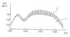
도 2는 페브리-페롯 레이저와 광섬유 증폭기를 결합한 전형적인 다중채널 광원을 나타내는 도면이고, 도 3은 도2에 도시된 광원의 출력 특성을 나타내는 도면이다.FIG. 2 illustrates a typical multichannel light source combining a Fabry-Perot laser and an optical fiber amplifier, and FIG. 3 illustrates output characteristics of the light source illustrated in FIG.
상기 다중채널 광원(100)은 페브리-페롯 레이저(Fabry-Perot laser: FP-LS, 110)와, 이에 하이브리드로 결합된 어븀 도핑된 광섬유 증폭기(Erbium-doped fiber amplifier: EDFA, 120)를 포함한다.The
상기 페브리-페롯 레이저(110)는 기설정된 페브리-페롯 모드들을 가지며 상기 어븀 도핑된 광섬유 증폭기(120)로부터 입력된 증폭된 자발 방출광(A)에 의해 생성된 분할광(B)을 출력한다.The Fabry-
상기 어븀 도핑된 광섬유 증폭기(120)는 상기 페브리-페롯 레이저(110)에 제 공하기 위한 증폭된 자발 방출광(A)을 생성하고, 페브리-페롯 레이저(110)로부터 입력된 분할광(B)을 증폭하여 출력한다.The erbium-doped
상기 분할광(B)은 다시 어븀 도핑된 광섬유 증폭기(120)에서 입력되어 증폭된 다중 채널광(C)으로 출력된다.The split light B is input from the erbium-doped
도 3은 상기 다중채널 광원(100)에서 출력된 증폭된 다중 채널광(C)의 파장 대 파워를 나타낸 도면이다. 상기 증폭된 다중 채널광(C)은 페브리-페롯 모드의 성분(3)과 자발 방출광의 성분(4)으로 구성되어 있다. 상기 증폭된 다중 채널광(C)은 페브리-페롯 모드의 성분(3)을 포함하고 있으므로 도 1에 나타난 것처럼 증폭된 자발 방출광의 성분만을 가지는 광보다 더 나은 전송 특성을 가질 수 있다.3 is a view showing the wavelength versus power of the amplified multi-channel light (C) output from the multi-channel light source (100). The amplified multi-channel light (C) consists of component (3) of Fabry-Perot mode and component (4) of spontaneous emission light. Since the amplified multi-channel light C includes the component 3 of the Fabry-Perot mode, it may have better transmission characteristics than the light having only the component of the amplified spontaneous emission light as shown in FIG. 1.
그러나, 도 2에서 제안된 다중채널 광원(100)은 전류가 주입되어야 하는 두 개의 능동 소자(110,120)를 하이브리드로 결합한 소자이기 때문에 비용이 높고, 페브리-페롯 레이저 모드의 파워가 항상 일정하지 않아 상대적인 광 파워에 의한 잡음(relative intensity noise: RIN)이 많기 때문에 광원의 효율이 낮다는 문제점이 있다.However, the
본 발명은 상술한 종래의 문제점을 해결하기 위하여 안출한 것으로, 본 발명의 목적은 가격이 저렴하고 고효율을 갖는 반도체 광증폭기 광원을 제공함에 있다.The present invention has been made to solve the above-mentioned conventional problems, and an object of the present invention is to provide a semiconductor optical amplifier light source having a low cost and high efficiency.
상기 목적을 달성하기 위하여, 본 발명에 따른 반도체 광증폭기 광원은, 증폭된 자발 방출광(amplified spontaneous emission: ASE)을 생성 및 증폭하기 위한 투과형 반도체 광증폭기와, 상기 투과형 반도체 광증폭기로부터 출력된 ASE를 스펙트럼 분할하여 스펙트럼 분할된 ASE를 생성하고, 상기 스펙트럼 분할된 ASE를 상기 투과형 반도체 광증폭기로 입력시키기 위한 파장분할다중 반사기를 포함한다.
In order to achieve the above object, the semiconductor optical amplifier light source according to the present invention, a transmissive semiconductor optical amplifier for generating and amplified amplified spontaneous emission (ASE) and the ASE output from the transmissive semiconductor optical amplifier Spectral division to generate a spectral partitioned ASE and include a wavelength division multiple reflector for inputting the spectral partitioned ASE to the transmission type semiconductor optical amplifier.
이하에서는 첨부도면들을 참조하여 본 발명의 실시예를 상세히 설명하기로 한다. 본 발명을 설명함에 있어서, 관련된 공지 기능이나 구성에 대한 구체적인 설명은 본 발명의 요지를 모호하지 않게 하기 위하여 생략한다.Hereinafter, with reference to the accompanying drawings will be described an embodiment of the present invention; In describing the present invention, detailed descriptions of related well-known functions and configurations are omitted in order not to obscure the subject matter of the present invention.
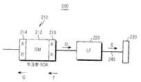
도 4는 본 발명의 바람직한 제1 실시예에 따른 반도체 광증폭기 광원을 나타내는 도면이다. 상기 반도체 광증폭기 광원(200)은 광도파로(240)를 통해 서로 연결된 투과형 반도체 광증폭기(210)와, 손실 필터(220) 및 파장분할다중(wavelength division multiplex: WDM) 반사기(230)를 포함한다. 연결 수단으로써 광도파로를 사용하는 것은 선택적인 것으로, 광도파로를 사용하지 않고 직접적으로 광을 입출력하는 방식이 가능하다. 이러한 경우 광을 집속하기위한 하나 이상의 렌즈를 포함할 수 있다.4 is a view showing a semiconductor optical amplifier light source according to a first embodiment of the present invention. The semiconductor optical
상기 투과형 반도체 광증폭기(210)는 이득 매질(212)과, 상기 이득 매질(212)의 양단에 코팅된 제1 및 제2 무반사층들(antireflection layer: AR, 214, 216)을 포함하며, 상기 투과형 반도체 광증폭기(210)는 상기 손실 필터(wavelength selective loss filter: WSLF, 220)와 상기 광도파로(240)를 통해 광학적으로 연결된다.The transmission type semiconductor
상기 투과형 반도체 광증폭기(210)는 상기 제1 및 제2 무반사층들(214, 216)을 통해 비간섭성 증폭된 자발 방출광(D)을 출력한다. 상기 투과형 반도체 광증폭기(210)의 제2 무반사층(216)으로부터 출력된 상기 증폭된 자발 방출광(D)의 파워는 전체 파장에 대해 일정하지 않고 도 5에 나타난 것처럼 넓은 대역에 걸쳐서 균일하지 않은 파워 프로파일을 갖는다. 또한 상기 투과형 반도체 광증폭기(210)는 상기 파워 프로파일과 유사한 모양의 이득 프로파일을 갖는다.The transmissive semiconductor
도 5는 도 4에 도시된 증폭된 자발 방출광(D)의 파워 프로파일을 나타내는 도면이다. 증폭된 자발 방출광(D)의 사용 파장 대역은 λ1, λ3을 끝단 파장으로 하고 상기 끝단 파장(λ1, λ3) 사이에 피크 파장(λ2)을 가진다. 상기 피크 파장(λ2)은 상기 사용 파장 대역에서 최대의 파워(피크 파워)를 가지며, 상기 끝단 파장(λ1, λ3)은 최소의 파워(끝단 파워)를 갖는다. 따라서 상기 증폭된 자발 방출광(D)의 파워 프로파일은 피크 파장(λ2)을 중심으로 대략 대칭적인, 위로 볼록한 형상의 모양을 나타낸다. 상기 피크 파장(λ2)의 파워와 끝단 파장(λ1, λ3)의 파워 사이에는 ΔP1 dB 만큼의 차이가 존재하게 된다. 이러한 파워의 차이는 결과적으로 상기 반도체 광증폭기 광원의 효율을 떨어뜨린다. 파워의 차이가 존재하게 될 경우 실질적으로 끝단 파장(λ1, λ3)의 파워 이하의 값들이 유용하게 사용될 수 있지만 피크 파워와 끝단 파워 사이의 값들은 버려지는 손실이 된다.FIG. 5 is a diagram showing a power profile of the amplified spontaneous emission light D shown in FIG. 4. The wavelength band of the amplified spontaneous emission light D used is λ1 , λ3 as the end wavelength and has a peak wavelength λ2 between the end wavelengths λ1 , λ3 . The peak wavelength λ2 has the maximum power (peak power) in the wavelength band used, and the end wavelengths λ1 , λ3 have the minimum power (end power). Thus, the power profile of the amplified spontaneous emission D exhibits an upwardly convex shape that is approximately symmetric about the peak wavelength λ2 . A difference of ΔP1 dB exists between the power of the peak wavelength λ2 and the power of the end wavelengths λ1 , λ3 . This difference in power results in a decrease in the efficiency of the semiconductor optical amplifier light source. If there is a difference in power, values substantially below the power of the end wavelengths λ1 and λ3 may be useful, but the values between the peak power and the end power are lost.
상기 손실 필터(220)는 상기 투과형 반도체 광증폭기(210)와 상기 파장분할 다중 반사기(230) 사이에 위치하며 상기 광도파로(240)를 통해 광학적으로 연결된다. 상기 손실 필터(220)는 기설정된 반사도 프로파일에 따라 상기 투과형 반도체 광증폭기(210)로부터 출력된 상기 증폭된 자발 방출광(D)과 상기 파장분할다중 반사기(230)로부터 반사된 제1 감쇄광(E)을 감쇄시킨다. 즉 상기 투과형 반도체 광증폭기(210)로부터 출력된 증폭된 자발 방출광(D)은 손실 필터(220)에서 두 번의 파워 감쇄 과정을 거친 후 다시 상기 투과형 반도체 광증폭기(210)에 입력된다. 상기 투과도 프로파일은 상기 광원(220)으로부터 출력되는 증폭된 제2 감쇄광이 평탄한 파워 프로파일을 가질 수 있도록 설정된 오목한 형상을 갖는다. 바닥 투과도와 끝단 투과도의 차이가 상기 증폭된 자발 방출광(D)의 피크 파워와 끝단 파워의 차이에 해당하는 것으로 설정된다. 상기 손실 필터(220)는 파장 간의 파워의 차이를 감쇄시킴으로써 파워의 손실을 줄여 광원의 효율을 증가시키는 역할을 한다. 바람직하게 상기 손실 필터(220)는 광섬유 또는 평면 광파 회로(planar lightwave circuit: PLC)에 장주기 격자(long period grating)를 사용하는 것을 포함한다.The
상기 파장분할다중 반사기(230)는 상기 손실 필터(220)와 상기 광도파로(240)를 통해 광학적으로 연결된다. 상기 파장분할다중 반사기(230)는 상기 손실 필터(220)로부터 출력된 제1 감쇄광(E)을 스펙트럼 분할하여 반사된 제1 감쇄광(E)을 생성하고, 상기 스펙트럼 분할된 제1 감쇄광(E)을 상기 손실 필터(220)로 입력시킨다. 상기 파장분할다중 반사기(230)로는 페브리-페롯 필터를 포함한다. 상기 파장분할다중 반사기(230)는 기설정된 반사 스펙트럼을 가지며 바람직하게 상기 반사 스펙트럼은 페브리-페롯 프린지(Fabry-Perot fringe)를 나타낸다. 즉, 상기 반 사 스펙트럼이란 피크 반사도를 나타내는 피크 파장들이 기설정된 간격으로 주기적으로 배열된 형상을 나타낸다.The wavelength split
정리하면 상기 파장분할다중 반사기(230)에 입력된 제1 감쇄광(E)은 상기 기설정된 반사 스펙트럼, 다시 말해 페브리-페롯 프린지(Fabry-Perot fringe)로 분할되어 반사된 후, 다시 상기 파장 선택적 필터(220)에 입력된다.In summary, the first attenuated light E input to the wavelength division
도 6은 도 4에 도시된 제2 감쇄광(F)의 파워 프로파일을 나타내는 도면으로 상기 증폭된 자발 방출광(D)이 두 번의 감쇄 과정을 거쳐 생성된 제2 감쇄광(F)을 보여준다. 상기 제2 감쇄광(F)은 도 5에서 최대의 파워를 가졌던 파장(λ2)을 중심으로 대략 대칭적인, 아래로 오목한 형상을 갖는다. 즉, 상기 끝단 파장(λ1, λ3)의 파워가 피크 파장(λ2)의 파워보다 더 큰 값을 가지며 그 차이는 ΔP2 dB 이다. 도 5의 파워 프로파일과는 달리 제2 감쇄광(D)은 상기 파장분할다중 반사기(230)에 의해 스펙트럼 분할되었기 때문에 프린지 형상을 가진다. 상기 손실 필터(220)에 의해 일차 감쇄 과정을 거친 제1 감쇄광(E)은 도시하지는 않았지만 끝단 파장(λ1, λ3)의 파워와 피크 파장(λ2)의 파워의 차이가 ΔP2/2 dB에 가까운 파워 프로파일을 갖게 될 것이다. 이러한 파워 프로파일을 갖는 제1 감쇄광(E)은 상기 파장분할다중 반사기(230)에 반사되어 다시 손실 필터(220)로 입력된다. 이차 감쇄 과정을 거쳐 상기 손실 필터(220)로부터 출력되는 제2 감쇄광(F)의 파워 프로파일은 도 6과 같은 오목한 형상을 갖는다.FIG. 6 is a view showing a power profile of the second attenuated light F shown in FIG. 4, and shows the second attenuated light F generated by the amplified spontaneous emission light D through two attenuation processes. The second attenuated light F has a concave downward shape that is approximately symmetric about the wavelength λ2 having the maximum power in FIG. 5. That is, the power of the end wavelengths λ1 and λ3 has a larger value than the power of the peak wavelength λ2 and the difference is ΔP2 dB. Unlike the power profile of FIG. 5, the second attenuated light D has a fringe shape because the second attenuated light D is spectrally divided by the wavelength division
도 7은 도 4에 도시된 증폭된 제2 감쇄광(G)의 파워 프로파일을 나타내는 도면이다. 상기 제2 감쇄광(F)은 상기 투과형 반도체 광증폭기(210)에 의해 증폭된 후 증폭된 제2 감쇄광(G)으로 출력되고 끝단 파장(λ1, λ3)의 파워와 피크 파장(λ2)의 파워의 차이가 없어진 수평한 파워 프로파일을 갖는다.FIG. 7 is a diagram illustrating a power profile of the amplified second attenuated light G shown in FIG. 4. The second attenuated light F is amplified by the transmission type semiconductor
정리하자면, 증폭된 자발 방출광(D)은 상기 손실 필터(220), 상기 파장분할다중 반사기(230) 및 상기 손실 필터(220)를 차례로 통과하면서 일정한 파워를 갖는 제1 감쇄광(E)으로 감쇄되고, 기설정된 반사 스펙트럼으로 분할된 후, 다시 감쇄되는 과정을 거치게 된다. 최종적으로 출력되는 증폭된 제2 감쇄광(G)은 파장에 대해 균일한 파워 프로파일을 갖는다.In summary, the amplified spontaneous emission light D passes through the
도 8에 도시된 증폭된 자발 방출광의 파워 프로파일은 반도체 광증폭기(210)로부터 출력된 증폭된 자발 방출광(D)이 상기 도 4의 손실 필터(220)를 거치지 않고 파장분할다중 반사기(230)에 반사되어 증폭된 결과를 나타낸다. 상기 증폭된 자발 방출광(D)은 상기 파장분할다중 반사기(230)에 의해 반사 스펙트럼 분할되었기 때문에 평탄하지 않은 프린지 형상을 가지고 있으나, 손실 필터(220)에 의한 파워 감쇄 과정을 거치지 않아 끝단 파워와 피크 파워 사이에는 ΔP3 dB의 차이가 존재한다. 도 5의 넓은 대역 광이 파장분할방식 필터(220)를 통과하면 반사 스펙트럼 분할될 수는 있어도 상기 손실 필터(230)를 통과하지 않는다면 파장에 따른 파워 손실을 피할 수 없게 되고 광원의 효율은 떨어진다.The power profile of the amplified spontaneous emission light shown in FIG. 8 shows that the amplified spontaneous emission light D output from the semiconductor
도 9는 도 4에 도시된 손실 필터의 파장에 따른 파워 투과도를 나타내는 도 면으로, 피크 파장(λ2)에서의 파워 투과도(바닥 투과도)가 끝단 파장들(λ1, λ3)의 파워 투과도(끝단 투과도)보다 낮은 아래로 오목한 형성을 보이고 있다. 파워 투과도란 상기 손실 필터(220)에 의해 감쇄되는 정도를 나타내는 것으로, 파워 투과도가 높으면 파워의 감쇄 정도가 낮고, 파워 투과도가 낮으면 파워의 감쇄 정도가 높은 것을 의미한다. 상기 증폭된 자발 방출광(D)의 피크 파워는 끝단 파워보다 파워 투과도가 낮기 때문에 상기 손실 필터(220)를 거치면서 파워가 감쇄되는 정도가 커지게 된다. 마찬가지로, 상기 제1 감쇄광(E)의 경우 피크 파장(λ2)에서의 파워 투과도가 낮아 파워가 감쇄되는 정도가 높기 때문에 상기 손실 필터(220)를 거쳐 출력된 제2 감쇄광(F)은 도 6과 같은 오목한 파워 프로파일은 갖는다.FIG. 9 is a diagram illustrating power transmittance according to the wavelength of the loss filter illustrated in FIG. 4, wherein the power transmittance (bottom transmittance) at the peak wavelength λ2 is the power transmittance of the end wavelengths λ1 and λ3 . A concave downward formation below (end permeability) is shown. The power transmittance represents the degree of attenuation by the
상기 증폭된 자발 방출광(D)이 상기 투과형 반도체 광증폭기(210)에서 증폭될 때, 상기 손실 필터(220)를 거치지 않을 경우에는 피크 파장(λ2)의 증폭된 자발 방출광은 보다 낮은 파워를 가졌던 끝단 파장들(λ1, λ3)의 증폭된 자발 방출광 보다 많은 carrier 소모가 발생한다. 하지만 상기 손실 필터(220)를 사용하여 피크 파장(λ2)의 자발 방출광의 파워를 낮추면, 이로 인해 절약되는 상기 반도체 광증폭기(210) 내의 carrier가 낮은 파워를 가졌던 끝단 파장(λ1, λ3) 부분의 자발 방출광의 파워를 높이는데 사용될 수 있다. 따라서 전체적인 스펙트럼 파워 레벨이 올라갈 수 있는 것이다.When the amplified spontaneous emission light D is amplified by the transmission type semiconductor
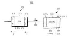
도 10은 본 발명의 바람직한 제2 실시예에 따른 반도체 광증폭기 광원을 나 타내는 도면으로 상기 반도체 광증폭기 광원(300)은 광도파로(330)를 통해 서로 연결된 투과형 반도체 광증폭기(310) 및 파장분할다중 반사기(320)를 포함한다.10 is a view showing a semiconductor optical amplifier light source according to a second embodiment of the present invention. The semiconductor optical
상기 투과형 반도체 광증폭기(310)는 이득 매질(312)과, 상기 이득 매질(312)의 양단에 코팅된 제1 및 제2 무반사층들(314, 316)을 포함하며, 상기 파장분할다중 반사기(320)와 상기 광도파로(330)를 통해 광학적으로 연결된다.The transmissive semiconductor
상기 투과형 반도체 광증폭기(310)는 상기 제1 및 제2 무반사층들(314, 316)을 통해 비간섭성 증폭된 자발 방출광(H)을 출력한다. 상기 투과형 반도체 광증폭기(310)의 제2 무반사층(316)으로 출력된 상기 증폭된 자발 방출광(H)은 도 5에 나타난 것처럼 넓은 대역 광으로 출력된다.The transmissive semiconductor
상기 파장분할다중 반사기(320)는 페브리-페롯 필터(Fabry-Perot filter: FP-FT, 322) 및 다중적층막(multiple coating layer: MCL, 324)을 포함하고, 상기 반도체 광증폭기(310)와 상기 광도파로(330)를 통해 광학적으로 연결된다. 파장분할다중 반사기(320)는 상기 반도체 광증폭기(310)로부터 출력된 증폭된 자발 방출광(H)을 스펙트럼 분할하여 반사된 감쇄광(I)을 생성하고, 상기 스펙트럼 분할된 감쇄광(I)을 상기 반도체 광증폭기(310)로 입력시킨다. 상기 파장분할다중 반사기(320)는 기설정된 반사 스펙트럼을 가지며, 상기 반사 스펙트럼이란 페브리-페롯 프린지(Fabry-Perot fringe)를 나타내는 것으로 피크 반사도를 나타내는 피크 파장들이 기설정된 간격으로 주기적으로 배열된 형상을 의미한다.The wavelength split
상기 페브리-페롯 필터(322)는 공동(cavity, 3224)과, 상기 공동 양측에 배치된 제1 및 제2 미러들(3224,3226)을 구비하며, 상기 제1 미러(3224)는 상기 반도 체 광증폭기(310)의 제2 무반사층(316)에 대향되게 배치되고, 상기 제2 미러(3226) 상에는 다중코팅막(324)이 적층된다. 상기 페브리-페롯 필터(322)는 파장분할다중 반사기(320)의 구성 요소로서 상기 증폭된 자발 방출광(H)에 기설정된 반사 스펙트럼 즉 페브리-페롯 프린지를 형성한다.The Fabry-
상기 다중적층막(324)은 상기 페브리-페롯 필터(322)의 제2 미러(3226) 상에 적층되고, 기설정된 반사도 프로파일에 따라 상기 파장분할다중 반사기에 입력된 증폭된 자발 방출광(H)을 감쇄시킨다. 상기 반사도 프로파일은 상기 광원으로부터 출력되는 증폭된 감쇄광이 평탄한 파워 프로파일을 가질 수 있도록 설정된 오목한 형상을 갖는다. 상기 다중적층막(324)은 파장에 따라 다른 반사도를 가지는 복수의 코팅층으로 이루어져 있으며 도 4에 나타난 손실 필터(220)의 역할을 한다. 도 10의 반도체 광증폭기 광원(300)은 파워 손실을 주는 필터(230)를 다중적층막(324)이 대신하게 되는 점만 다를 뿐 동작 원리는 도 4의 반도체 광증폭기 광원(200)과 같다.The
도 11은 도 10에 도시된 감쇄광(I)의 파워 프로파일을, 도 12는 도 10에 도시된 증폭된 감쇄광(J)의 파워 프로파일을 나타내는 도면으로 상기 도6 및 7과 동일하며 그 구성에 대한 설명도 같은 맥락을 이룬다. 상기 감쇄광(I)은 도 5에서 최대의 파워를 가졌던 파장(λ2)을 중심으로 대략 대칭적인, 아래로 오목한 형상을 갖는다. 즉, 상기 끝단 파장(λ1, λ3)의 파워가 피크 파장(λ2)의 파워보다 더 큰 값을 가지며 그 차이는 ΔP4 dB 이다. 도 5의 파워 프로파일과는 달리 감쇄광(I)은 상 기 파장분할다중 반사기(230)에 의해 스펙트럼 분할되었기 때문에 프린지 형상을 가진다. 상기 감쇄광(I)은 상기 투과형 반도체 광증폭기(210)에 의해 증폭된 후 증폭된 감쇄광(J)으로 출력되고 끝단 파장(λ1, λ3)의 파워와 피크 파장(λ2)의 파워의 차이가 없어진 수평한 파워 프로파일을 갖는다.FIG. 11 is a power profile of the attenuated light I shown in FIG. 10, and FIG. 12 is a power profile of the amplified attenuated light J shown in FIG. The same goes for the description. The attenuated light I has a concave downward shape that is approximately symmetric about the wavelength λ2 , which had the maximum power in FIG. 5. That is, the power of the end wavelengths λ1 and λ3 has a larger value than the power of the peak wavelength λ2 and the difference is ΔP4 dB. Unlike the power profile of FIG. 5, the attenuated light I has a fringe shape because it is spectrally divided by the wavelength division
정리하자면, 증폭된 자발 방출광(H)은 상기 손실 필터(220), 상기 파장분할다중 반사기(230)를 차례로 통과하면서 기설정된 반사 스펙트럼으로 분할되고, 감쇄되는 과정을 거치게 된다. 최종적으로 출력되는 증폭된 감쇄광(J)은 파장에 대해 균일한 파워 프로파일을 갖는다.In summary, the amplified spontaneous emission light H passes through the
도 13은 도 10에 도시된 다중적층막(324)의 파장에 따른 파워 반사도를 나타내는 도면으로 피크 파장(λ2)에서의 파워 반사도(바닥 반사도)가 끝단 파장들(λ1, λ3)의 파워 반사도(끝단 반사도)보다 낮은 아래로 오목한 형성을 보이고 있다. 파워 반사도란 상기 다중적층막(324)에 의해 감쇄되는 정도를 나타내는 것으로, 파워 반사도가 높으면 파워의 감쇄 정도가 낮고, 파워 반사도가 낮으면 파워의 감쇄 정도가 높은 것을 의미한다. 상기 증폭된 자발 방출광(H)의 피크 파워는 끝단 파워보다 파워 투과도가 낮기 때문에 상기 다중적층막(324)을 거치면서 파워가 감쇄되는 정도가 커지게 되고 출력된 감쇄광(I)은 도 11과 같은 오목한 파워 프로파일은 갖는다.FIG. 13 is a diagram illustrating power reflectance according to the wavelength of the
상술한 바와 같이, 본 발명에 따른 반도체 광증폭기 광원은 전류를 주입해야 하는 하나의 능동 소자를 사용하여 가격이 저렴하고, 파장분할다중 필터를 사용함으로써 우수한 전송 특성을 가지고, 손실 필터 또는 다중적층막을 사용하여, 종래에 비하여 안정적이고 효율적인 광파워를 얻을 수 있다는 이점이 있다. As described above, the semiconductor optical amplifier light source according to the present invention is inexpensive by using one active element to inject current, has excellent transmission characteristics by using a wavelength division multiplex filter, and has a loss filter or a multilayer film. By using this method, there is an advantage that a stable and efficient optical power can be obtained as compared with the prior art.
Claims (8)
Translated fromKoreanPriority Applications (1)
| Application Number | Priority Date | Filing Date | Title |
|---|---|---|---|
| KR1020040074553AKR100594059B1 (en) | 2004-09-17 | 2004-09-17 | Semiconductor optical amplifier |
Applications Claiming Priority (1)
| Application Number | Priority Date | Filing Date | Title |
|---|---|---|---|
| KR1020040074553AKR100594059B1 (en) | 2004-09-17 | 2004-09-17 | Semiconductor optical amplifier |
Publications (2)
| Publication Number | Publication Date |
|---|---|
| KR20060025753A KR20060025753A (en) | 2006-03-22 |
| KR100594059B1true KR100594059B1 (en) | 2006-06-30 |
Family
ID=37131149
Family Applications (1)
| Application Number | Title | Priority Date | Filing Date |
|---|---|---|---|
| KR1020040074553AExpired - Fee RelatedKR100594059B1 (en) | 2004-09-17 | 2004-09-17 | Semiconductor optical amplifier |
Country Status (1)
| Country | Link |
|---|---|
| KR (1) | KR100594059B1 (en) |
Families Citing this family (1)
| Publication number | Priority date | Publication date | Assignee | Title |
|---|---|---|---|---|
| WO2016033234A1 (en)* | 2014-08-26 | 2016-03-03 | C.R. Bard, Inc | Urinary catheter |
Citations (3)
| Publication number | Priority date | Publication date | Assignee | Title |
|---|---|---|---|---|
| JPS6164182A (en) | 1984-09-05 | 1986-04-02 | Matsushita Electric Ind Co Ltd | Optical feedback semiconductor laser device |
| JP2000261086A (en) | 1999-03-10 | 2000-09-22 | Nippon Telegr & Teleph Corp <Ntt> | Tunable light source |
| KR20020013660A (en)* | 2000-08-14 | 2002-02-21 | 윤덕용 | Multi-stage bidirectional optical amplifier |
- 2004
- 2004-09-17KRKR1020040074553Apatent/KR100594059B1/ennot_activeExpired - Fee Related
Patent Citations (3)
| Publication number | Priority date | Publication date | Assignee | Title |
|---|---|---|---|---|
| JPS6164182A (en) | 1984-09-05 | 1986-04-02 | Matsushita Electric Ind Co Ltd | Optical feedback semiconductor laser device |
| JP2000261086A (en) | 1999-03-10 | 2000-09-22 | Nippon Telegr & Teleph Corp <Ntt> | Tunable light source |
| KR20020013660A (en)* | 2000-08-14 | 2002-02-21 | 윤덕용 | Multi-stage bidirectional optical amplifier |
Also Published As
| Publication number | Publication date |
|---|---|
| KR20060025753A (en) | 2006-03-22 |
Similar Documents
| Publication | Publication Date | Title |
|---|---|---|
| US6195200B1 (en) | High power multiwavelength light source | |
| US5936763A (en) | Optical fiber amplifier, semiconductor laser module for pumping and optical signal communication system | |
| US6433921B1 (en) | Multiwavelength pumps for raman amplifier systems | |
| CA2387645C (en) | Multiple wavelength optical sources | |
| Park et al. | Multiple wavelength operation of an erbium-doped fiber laser | |
| US6374006B1 (en) | Chirped period gratings for raman amplification in circulator loop cavities | |
| US5598294A (en) | Optical fiber amplifier and optical fiber communication system | |
| US7190861B2 (en) | Monolithic semiconductor light source with spectral controllability | |
| JP2005123612A (en) | Broadband light source using semiconductor optical amplifier | |
| US20020048300A1 (en) | Semiconductor laser device for use in a laser module | |
| US6529317B2 (en) | L-band erbium-doped fiber amplifier pumped by 1530 nm-band pump | |
| JPH10215017A (en) | Light source device, optical amplifier, and optical communication system | |
| KR100575966B1 (en) | Broadband light source | |
| US6496619B2 (en) | Method for gain equalization, and device and system for use in carrying out the method | |
| JPH1168215A (en) | Light generating system for optical fiber network | |
| KR100539927B1 (en) | Bi-directional wavelength division multiplexer system | |
| US7167302B2 (en) | Gain-flattened wideband erbium-doped optical fiber amplifier | |
| US7359638B2 (en) | Optical source generator for wavelength division multiplexing optical communication systems | |
| JP4118865B2 (en) | Multi-channel light source and multi-channel optical module using the same | |
| Lee et al. | Bandwidth optimization of a spectrum-sliced fiber amplifier light source using an angle-tuned Fabry-Perot filter and a double-stage structure | |
| US20040160994A1 (en) | Multiple wavelength laser system | |
| US7020168B2 (en) | High power multi-frequency laser | |
| WO2003044914A1 (en) | Multi-wavelength raman fiber laser | |
| KR100622015B1 (en) | Amplified spontaneous emission (ASE) reflective gain-fixed fiber amplifier | |
| KR100594059B1 (en) | Semiconductor optical amplifier |
Legal Events
| Date | Code | Title | Description |
|---|---|---|---|
| A201 | Request for examination | ||
| PA0109 | Patent application | St.27 status event code:A-0-1-A10-A12-nap-PA0109 | |
| PA0201 | Request for examination | St.27 status event code:A-1-2-D10-D11-exm-PA0201 | |
| PN2301 | Change of applicant | St.27 status event code:A-3-3-R10-R13-asn-PN2301 St.27 status event code:A-3-3-R10-R11-asn-PN2301 | |
| PN2301 | Change of applicant | St.27 status event code:A-3-3-R10-R13-asn-PN2301 St.27 status event code:A-3-3-R10-R11-asn-PN2301 | |
| PG1501 | Laying open of application | St.27 status event code:A-1-1-Q10-Q12-nap-PG1501 | |
| D13-X000 | Search requested | St.27 status event code:A-1-2-D10-D13-srh-X000 | |
| D14-X000 | Search report completed | St.27 status event code:A-1-2-D10-D14-srh-X000 | |
| E701 | Decision to grant or registration of patent right | ||
| PE0701 | Decision of registration | St.27 status event code:A-1-2-D10-D22-exm-PE0701 | |
| GRNT | Written decision to grant | ||
| PR0701 | Registration of establishment | St.27 status event code:A-2-4-F10-F11-exm-PR0701 | |
| PR1002 | Payment of registration fee | St.27 status event code:A-2-2-U10-U11-oth-PR1002 Fee payment year number:1 | |
| PG1601 | Publication of registration | St.27 status event code:A-4-4-Q10-Q13-nap-PG1601 | |
| LAPS | Lapse due to unpaid annual fee | ||
| PC1903 | Unpaid annual fee | St.27 status event code:A-4-4-U10-U13-oth-PC1903 Not in force date:20090621 Payment event data comment text:Termination Category : DEFAULT_OF_REGISTRATION_FEE | |
| PC1903 | Unpaid annual fee | St.27 status event code:N-4-6-H10-H13-oth-PC1903 Ip right cessation event data comment text:Termination Category : DEFAULT_OF_REGISTRATION_FEE Not in force date:20090621 | |
| R18-X000 | Changes to party contact information recorded | St.27 status event code:A-5-5-R10-R18-oth-X000 | |
| P22-X000 | Classification modified | St.27 status event code:A-4-4-P10-P22-nap-X000 | |
| P22-X000 | Classification modified | St.27 status event code:A-4-4-P10-P22-nap-X000 |