KR100591508B1 - Atomic layer deposition of oxide film - Google Patents
Atomic layer deposition of oxide filmDownload PDFInfo
- Publication number
- KR100591508B1 KR100591508B1KR1020040013705AKR20040013705AKR100591508B1KR 100591508 B1KR100591508 B1KR 100591508B1KR 1020040013705 AKR1020040013705 AKR 1020040013705AKR 20040013705 AKR20040013705 AKR 20040013705AKR 100591508 B1KR100591508 B1KR 100591508B1
- Authority
- KR
- South Korea
- Prior art keywords
- hafnium
- precursor
- oxide
- chamber
- containing precursor
- Prior art date
- Legal status (The legal status is an assumption and is not a legal conclusion. Google has not performed a legal analysis and makes no representation as to the accuracy of the status listed.)
- Expired - Fee Related
Links
Images


Classifications
- C—CHEMISTRY; METALLURGY
- C30—CRYSTAL GROWTH
- C30B—SINGLE-CRYSTAL GROWTH; UNIDIRECTIONAL SOLIDIFICATION OF EUTECTIC MATERIAL OR UNIDIRECTIONAL DEMIXING OF EUTECTOID MATERIAL; REFINING BY ZONE-MELTING OF MATERIAL; PRODUCTION OF A HOMOGENEOUS POLYCRYSTALLINE MATERIAL WITH DEFINED STRUCTURE; SINGLE CRYSTALS OR HOMOGENEOUS POLYCRYSTALLINE MATERIAL WITH DEFINED STRUCTURE; AFTER-TREATMENT OF SINGLE CRYSTALS OR A HOMOGENEOUS POLYCRYSTALLINE MATERIAL WITH DEFINED STRUCTURE; APPARATUS THEREFOR
- C30B25/00—Single-crystal growth by chemical reaction of reactive gases, e.g. chemical vapour-deposition growth
- C30B25/02—Epitaxial-layer growth
- C30B25/14—Feed and outlet means for the gases; Modifying the flow of the reactive gases
- C—CHEMISTRY; METALLURGY
- C23—COATING METALLIC MATERIAL; COATING MATERIAL WITH METALLIC MATERIAL; CHEMICAL SURFACE TREATMENT; DIFFUSION TREATMENT OF METALLIC MATERIAL; COATING BY VACUUM EVAPORATION, BY SPUTTERING, BY ION IMPLANTATION OR BY CHEMICAL VAPOUR DEPOSITION, IN GENERAL; INHIBITING CORROSION OF METALLIC MATERIAL OR INCRUSTATION IN GENERAL
- C23C—COATING METALLIC MATERIAL; COATING MATERIAL WITH METALLIC MATERIAL; SURFACE TREATMENT OF METALLIC MATERIAL BY DIFFUSION INTO THE SURFACE, BY CHEMICAL CONVERSION OR SUBSTITUTION; COATING BY VACUUM EVAPORATION, BY SPUTTERING, BY ION IMPLANTATION OR BY CHEMICAL VAPOUR DEPOSITION, IN GENERAL
- C23C16/00—Chemical coating by decomposition of gaseous compounds, without leaving reaction products of surface material in the coating, i.e. chemical vapour deposition [CVD] processes
- C23C16/44—Chemical coating by decomposition of gaseous compounds, without leaving reaction products of surface material in the coating, i.e. chemical vapour deposition [CVD] processes characterised by the method of coating
- C23C16/455—Chemical coating by decomposition of gaseous compounds, without leaving reaction products of surface material in the coating, i.e. chemical vapour deposition [CVD] processes characterised by the method of coating characterised by the method used for introducing gases into reaction chamber or for modifying gas flows in reaction chamber
- C23C16/45523—Pulsed gas flow or change of composition over time
- C23C16/45525—Atomic layer deposition [ALD]
- C23C16/45527—Atomic layer deposition [ALD] characterized by the ALD cycle, e.g. different flows or temperatures during half-reactions, unusual pulsing sequence, use of precursor mixtures or auxiliary reactants or activations
- C23C16/45531—Atomic layer deposition [ALD] characterized by the ALD cycle, e.g. different flows or temperatures during half-reactions, unusual pulsing sequence, use of precursor mixtures or auxiliary reactants or activations specially adapted for making ternary or higher compositions
- C—CHEMISTRY; METALLURGY
- C30—CRYSTAL GROWTH
- C30B—SINGLE-CRYSTAL GROWTH; UNIDIRECTIONAL SOLIDIFICATION OF EUTECTIC MATERIAL OR UNIDIRECTIONAL DEMIXING OF EUTECTOID MATERIAL; REFINING BY ZONE-MELTING OF MATERIAL; PRODUCTION OF A HOMOGENEOUS POLYCRYSTALLINE MATERIAL WITH DEFINED STRUCTURE; SINGLE CRYSTALS OR HOMOGENEOUS POLYCRYSTALLINE MATERIAL WITH DEFINED STRUCTURE; AFTER-TREATMENT OF SINGLE CRYSTALS OR A HOMOGENEOUS POLYCRYSTALLINE MATERIAL WITH DEFINED STRUCTURE; APPARATUS THEREFOR
- C30B25/00—Single-crystal growth by chemical reaction of reactive gases, e.g. chemical vapour-deposition growth
- C30B25/02—Epitaxial-layer growth
- C—CHEMISTRY; METALLURGY
- C30—CRYSTAL GROWTH
- C30B—SINGLE-CRYSTAL GROWTH; UNIDIRECTIONAL SOLIDIFICATION OF EUTECTIC MATERIAL OR UNIDIRECTIONAL DEMIXING OF EUTECTOID MATERIAL; REFINING BY ZONE-MELTING OF MATERIAL; PRODUCTION OF A HOMOGENEOUS POLYCRYSTALLINE MATERIAL WITH DEFINED STRUCTURE; SINGLE CRYSTALS OR HOMOGENEOUS POLYCRYSTALLINE MATERIAL WITH DEFINED STRUCTURE; AFTER-TREATMENT OF SINGLE CRYSTALS OR A HOMOGENEOUS POLYCRYSTALLINE MATERIAL WITH DEFINED STRUCTURE; APPARATUS THEREFOR
- C30B29/00—Single crystals or homogeneous polycrystalline material with defined structure characterised by the material or by their shape
- C30B29/10—Inorganic compounds or compositions
- C30B29/16—Oxides
Landscapes
- Chemical & Material Sciences (AREA)
- Engineering & Computer Science (AREA)
- Materials Engineering (AREA)
- Metallurgy (AREA)
- Organic Chemistry (AREA)
- Crystallography & Structural Chemistry (AREA)
- Chemical Kinetics & Catalysis (AREA)
- General Chemical & Material Sciences (AREA)
- Inorganic Chemistry (AREA)
- Mechanical Engineering (AREA)
- Formation Of Insulating Films (AREA)
- Chemical Vapour Deposition (AREA)
Abstract
Translated fromKoreanDescription
Translated fromKorean도 1 은 종래의 나노층 박막 증착 공정의 흐름도.1 is a flow chart of a conventional nanolayer thin film deposition process.
도 2 는 산화제로 질산염 전구체를 사용하여 나노층 박막을 증착하는 공정의 흐름도.2 is a flow chart of a process of depositing a nanolayer thin film using a nitrate precursor as an oxidant.
도 3 은 산화제로 질산화 하프늄 전구체를 사용하여, 나노층 박막을 증착하는 공정의 흐름도.3 is a flow chart of a process for depositing a nanolayer thin film using a hafnium nitride precursor as an oxidant.
도 4 는 질산화 하프늄 전구체 및 알루미늄 전구체를 사용하는 반도체 공정에 사용하기 위해, 산화 하프늄 / 산화 알루미늄 나노층 박막을 증착하는 공정의 흐름도.4 is a flow chart of a process for depositing a hafnium oxide / aluminum oxide nanolayer thin film for use in a semiconductor process using a hafnium nitride precursor and an aluminum precursor.
도 5a - 5d 는 반도체 게이트 유전체 응용에서의, 산화 하프늄 / 산화 알루미늄 나노층 박막 또는 산화 하프늄 박막의 증착 공정의 단계들을 도시한 도면.5A-5D illustrate steps of a deposition process of a hafnium oxide / aluminum oxide nanolayer thin film or hafnium oxide thin film in a semiconductor gate dielectric application.
도 6 은 본 발명의 방법을 이용하여 증착된, 4 nm 산화 하프늄 / 산화 알루미늄 나노층 박막의 커패시턴스 대 바이어스 전압의 선도.6 is a plot of capacitance versus bias voltage of a 4 nm hafnium oxide / aluminum oxide nanolayer thin film deposited using the method of the present invention.
도 7 은 동일한 4 nm 산화 하프늄 / 산화 알루미늄 나노층 박막에 대한, 누설 전류 대 바이어스 전압의 선도.7 is a plot of leakage current versus bias voltage for the same 4 nm hafnium oxide / aluminum oxide nanolayer thin film.
도 8 은 질산화 하프늄 전구체를 산화제로 사용하는 산화 하프늄 박막 증착 공정의 흐름도이다.8 is a flowchart of a hafnium oxide thin film deposition process using a hafnium nitride precursor as an oxidant.
도 9 는 질산화 하프늄 전구체 및 하프늄-함유 전구체을 사용하는 반도체 공정에 사용하기 위한 산화 하프늄 박막 증착 공정의 흐름도이다.9 is a flow chart of a hafnium oxide thin film deposition process for use in a semiconductor process using a hafnium nitride precursor and a hafnium-containing precursor.
도 10 은 산화 하프늄 박막을 위한 증착 두께 대 증착 싸이클의 플롯을 도시한다.10 shows a plot of deposition thickness versus deposition cycle for a hafnium oxide thin film.
※ 도면의 주요부분에 대한 부호의 설명※ Explanation of code for main part of drawing
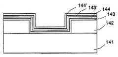
140: 수소-종단 실리콘 표면 141: 실리콘 기판140: hydrogen-terminated silicon surface 141: silicon substrate
142: 필드 산화물 143: 산화 하프늄 층142: field oxide 143: hafnium oxide layer
144: 산화 알루미늄 층 143': 산화 하프늄의 또다른 층144: aluminum oxide layer 143 ': another layer of hafnium oxide
144': 산화 알루미늄의 또다른 층144 ': another layer of aluminum oxide
발명의 분야Field of invention
본 발명은, 질산화 금속-함유 전구체 (precursor) 를 또다른 금속-함유 전구체를 위한 산화제로 이용하여, 산화 금속 나노층 박막 (nanolaminate film) 을 증착시키는 원자층 증착 (ALD; atomic layer deposition) 방법에 관한 것이다. 본 발명은, 야금술 및 생물의학 응용을 위한 전기-광학 구조, 광학 코팅, 및 패시베이션 코팅 (passivation coating) 을 포함한 다양한 응용에서 사용될 수 있다. 특히, 본 발명은 집적 회로 제조에 관한 것이로, 구체적으로는 반도체 트랜지스터용의 게이트 유전체 (gate dielectric) 및 메모리 회로에 대한 커패시터 유전체에 관한 것이다.The present invention relates to an atomic layer deposition (ALD) method in which a metal oxide nanolayer thin film is deposited using a metal nitrate-containing precursor as an oxidant for another metal-containing precursor. It is about. The present invention can be used in a variety of applications, including electro-optical structures, optical coatings, and passivation coatings for metallurgical and biomedical applications. In particular, the present invention relates to integrated circuit fabrication, and more particularly, to a gate dielectric for semiconductor transistors and a capacitor dielectric for memory circuits.
발명의 배경Background of the Invention
집적 회로에서 반도체 장치 내의 유전체 물질은 전계 효과 트랜지스터 (FET; field effect transistor) 용의 게이트 유전체 및 동적 랜덤 액세스 메모리 (dynamic random access memory) 용의 커패시터 유전체로 분류된다. 이러한 유전체의 크기 (dimensions) 는 반도체 장치의 성능과 직접적으로 관련된다. 더 빠른 응답 및 더 복잡한 기능을 달성하기 위해, 오늘날의 집적회로 제조는 두께뿐만 아니라 측면 크기의, 모든 방향에 있어 더 작아지고 있다.In an integrated circuit, dielectric materials in semiconductor devices are classified into gate dielectrics for field effect transistors (FETs) and capacitor dielectrics for dynamic random access memory. The dimensions of these dielectrics are directly related to the performance of the semiconductor device. In order to achieve faster response and more complex functions, today's integrated circuit fabrication is becoming smaller in all directions, not only in thickness but also in side dimensions.
DRAM 장치의 성능은 커패시터에 저장된 전하와 관련되고, 이는 커패시터의 면적 및 유전 상수 k 에 정비례하고 커패시터의 두께에는 반비례한다. 커패시터의 크기가 줄어듬에 따라, 고 성능 DRAM 장치에 적합한 커패시턴스 전하를 유지하기 위해, 커패시터 유전체로서 높은 k 유전체가 매우 바람직하다.The performance of a DRAM device is related to the charge stored in the capacitor, which is directly proportional to the area and dielectric constant k of the capacitor and inversely proportional to the thickness of the capacitor. As capacitors shrink in size, high k dielectrics are highly desirable as capacitor dielectrics to maintain capacitance charges suitable for high performance DRAM devices.
반도체 장치의 속도는, 전압을 인가한 후 FET 내의 게이트 유전체의 응답에 정비례한다. 게이트 유전체의 응답은 유전 상수 k 에 정비례하고 유전체의 두께 t 에 반비례한다. 따라서, 얇고 높은 k 의 유전체에 대한 필요성이 게이트 유전체로서 매우 요망되고 있다.The speed of the semiconductor device is directly proportional to the response of the gate dielectric in the FET after applying a voltage. The response of the gate dielectric is directly proportional to the dielectric constant k and inversely proportional to the thickness t of the dielectric. Thus, the need for thin, high k dielectrics is highly desired as gate dielectrics.
게이트 유전체의 주 재료는 약 4 의 유전 상수를 갖는 산화 실리콘 (SiO2) 이다. 장치 크기가 계속적으로 줄어듬에 따라, 산화 실리콘 게이트 유전체의 두께는 1.5 ∼ 2 nm 의 터널링 한계 (tunneling limit) 까지 도달했다. 일반적 으로, 1.5 nm 보다 적은 산화 실리콘 막은, 직접 터널링 전류 (direct tunneling currents) 로부터의 높은 누설로 인한 과도한 전력 소비로 인해, FET 장치에서 게이트 유전체로서 주로 사용할 수 없다. 또한, 붕소 페너트레이션 (boron penetration), 전하 주입 손상 (charge injection damage) 과 같은, 이러한 초 박 산화 실리콘 막과 관련한 제조 및 신뢰성의 염려가 존재한다.The main material of the gate dielectric is silicon oxide (SiO2 ) with a dielectric constant of about four. As the device size continues to shrink, the thickness of the silicon oxide gate dielectric has reached a tunneling limit of 1.5 to 2 nm. In general, silicon oxide films of less than 1.5 nm cannot be used primarily as gate dielectrics in FET devices due to excessive power consumption due to high leakage from direct tunneling currents. There are also concerns of manufacturing and reliability associated with such ultra thin silicon oxide films, such as boron penetration, charge injection damage.
산화 실리콘에 대한, 가능한 대체물로서, 여러가지 높고 일정한 유전체 재료 (높은 k 유전체) 를 연구하였으나, 낮은 누설 전류, 실리콘 기판과의 양호한 계면의 형성, 제조 공정에서의 낮은 열 한계 (low thermal budget) 및 디바이스 하이 채널 이동도 (device high channel mobility) 와 같은 여러가지 엄격한 요구사항 때문에, 아직까지 적당한 대체물을 발견하지 못하고 있다. 잠재적인 후보는 산화 티타늄 (TiO2), 산화 탄탈륨 (9 내지 27 사이의 k 값을 갖는 Ta2O5), 산화 알루미늄 (약 9 의 k 값을 갖는 Al2O3), 산화 지르코늄 (10 내지 25 사이의 k 값을 갖는 ZrO2), 산화 하프늄 (10 내지 25 사이의 k 값을 갖는 HfO2) 과 다층 (multilayer), 멀티콤포넌트 및 나노층과 같은 다양한 조합물과 혼합물이다.As a possible alternative to silicon oxide, various high and constant dielectric materials (high k dielectrics) have been studied, but low leakage currents, formation of good interfaces with silicon substrates, low thermal budgets in the manufacturing process and devices Due to various stringent requirements such as device high channel mobility, no suitable alternative has yet been found. Potential candidates are titanium oxide (TiO2 ), tantalum oxide (Ta2 O5 with a k value between 9 and 27), aluminum oxide (Al2 O3 with a k value of about 9), zirconium oxide (10 to ZrO2 ) having a k value between 25, hafnium oxide (HfO2 having a k value between 10 and 25) and mixtures and mixtures with various combinations such as multilayers, multicomponents and nanolayers.
현재의, 게이트 유전체 응용을 위한 높은 k 유전체 재료로서 선도적인 후보는 산화 지르코늄 및 산화 하프늄이다. 이들 재료의 벌크 유전 상수의 크기는 약 20 내지 25 로서, 약 5 내지 6 nm 인 이러한 재료는 두께가 1 nm 인 산화 실리콘과 등가임을 의미한다.Currently, leading candidates for high k dielectric materials for gate dielectric applications are zirconium oxide and hafnium oxide. The bulk dielectric constant of these materials is about 20 to 25, meaning that such materials of about 5 to 6 nm are equivalent to silicon oxide having a thickness of 1 nm.
ALD 를 통하여 증착된 지르코늄 산화 막은, 높은 유전 상수 및 낮은 누설을 포함하는, 양호한 절연 특성을 나타낸다. 그러나, 큰 문제는 수소-종단 표면 상에 부드럽게 직접 증착하지 못하며, 대신 균일한 시작 (uniform initiation) 을 위하여 산화 실리콘의 박층 (thin layer) 을 요구하는 것이다. 이의 예가, Electrochemical and Solid-State Letters, 5 (5), C57-59 (2002) 에 실린 Conley 등의 "Atomic layer deposition of hafnium oxide using anhydrous hafnium nitrate" 에 개시되어 있다. 얇은 산화 실리콘 계면 층이 존재한다면, 1 nm 의 등가 두께인 산화 실리콘을 얻는 것은 매우 어렵기 때문에, 그 존재는 바람직하지 않다. 수소-종단 실리콘 표면은, 실리콘의 댕글링 본드 (dangling bonds) 가 수소로 종단되어 있는, 어떠한 고유의(native) 산화 실리콘도 없는, 실리콘 표면이다. 수소-종단 실리콘 표면은 표준 산업 반도체 세정 공정의 결과물이다. 이러한 표준 세정 공정은 통상적으로 실리콘 웨이퍼를 HF 용액에 급속 침적 (quick immersions) 하여, 수소 패시베이션 (hydrogen passivation) 으로도 알려진 수소로 종단된 실리콘 표면을 생성한다.Zirconium oxide films deposited through ALD exhibit good insulation properties, including high dielectric constant and low leakage. However, a big problem is that it does not deposit directly directly on the hydrogen-terminated surface, but instead requires a thin layer of silicon oxide for uniform initiation. Examples thereof are disclosed in "Atomic layer deposition of hafnium oxide using anhydrous hafnium nitrate" by Conley et al. In Electrochemical and Solid-State Letters, 5 (5), C57-59 (2002). If a thin silicon oxide interfacial layer is present, its presence is undesirable since it is very difficult to obtain silicon oxide with an equivalent thickness of 1 nm. The hydrogen-terminated silicon surface is any inherent element in which dangling bonds of silicon are terminated with hydrogen. It is a silicon surface without native silicon oxide. Hydrogen-terminated silicon surfaces are the result of standard industrial semiconductor cleaning processes. These standard cleaning processes typically rapidly immerse silicon wafers in HF solution, producing hydrogen terminated silicon surfaces, also known as hydrogen passivation.
산화 하프늄에 대한 연구는, 적합한 증착 조건하에서, 수소-종단된 실리콘 표면 상에, 매끄럽고 균일한 아몰퍼스 하프늄 산화 막을 직접 증착할 수 있음을 알려준다. 10.5 의 유전 상수 및 2.1 nm 의 커패시턴스 등가 두께를, 수소-종단 실리콘 표면 상에 5.7 nm 두께의 산화 하프늄을 직접 증착하여 달성하였다. 이는, 더 연구하면 등가 두께를 1 nm 이하로 줄일 수 있다는 것을 알려주기 때문에, 매우 바람직한 특성이다. 그러나, 증착된 하프늄 산화 막은 여전히 여러가지 문제점을 갖고 있다. 한 문제점은, 반도체 장치의 제조 공정에서 더 낮은 온도 한계 (lower thermal budget) 를 초래하는 낮은 결정화 온도이다. 또다른 문제점은 산화 하프늄과 실리콘 기판의 계면의 품질이 산화 실리콘과 실리콘 기판의 계면에 비해 상대적으로 열악하다는 것이다. 이것은 반도체 장치 구조로 집적될 때 낮은 채널 이동도를 초래한다.Studies on hafnium oxide show that it is possible to deposit a smooth, uniform amorphous hafnium oxide film directly on a hydrogen-terminated silicon surface under suitable deposition conditions. A dielectric constant of 10.5 and a capacitance equivalent thickness of 2.1 nm were achieved by direct deposition of 5.7 nm thick hafnium oxide on the hydrogen-terminated silicon surface. This is a very desirable property since further research indicates that the equivalent thickness can be reduced to 1 nm or less. However, the deposited hafnium oxide film still has various problems. One problem is the low crystallization temperature which results in a lower thermal budget in the manufacturing process of semiconductor devices. Another problem is that the quality of the interface between hafnium oxide and the silicon substrate is relatively poor compared to the interface between silicon oxide and the silicon substrate. This results in low channel mobility when integrated into the semiconductor device structure.
얇은 교번 절연체 층 (alternating layers of insulators) 은, 그 특성이 조정될 수 있는 혼성 막 (즉, 나노층) 을 형성할 수 있음을 나타내고 있다. 2000 년 2 월 15 일에 Journal of Applied Physics, Vol. 87, No 4 에 실린 Zhang 등의 "high permittivity thin film nanolaminates" 의 종래 연구는, Ta2O5-HfO2, ZrO2-HfO2, 및 Ta2O5-ZrO2의 나노층은 나노층의 두께에 의존하여 다른 특성을 나타냄을 알려준다.Thin alternating layers of insulators have shown that they can form hybrid films (ie nanolayers) whose properties can be adjusted. On February 15, 2000, Journal of Applied Physics, Vol. Previous studies of "high permittivity thin film nanolaminates" by Zhang et al., 87, No. 4, disclose that the nanolayers of Ta2 O5 -HfO2 , ZrO2 -HfO2 , and Ta2 O5 -ZrO2 are composed of nanolayers. Depending on the thickness, it shows different characteristics.
또한, 종래 연구는, 알루미늄을 도핑하여, 높은 k 유전체 막의 특성을 변경할 수 있음을 알려준다. 예를 들어, Ma 등의, 발명의 명칭이 "Aluminum-doped zirconium dielectric film transistor structure and deposition method for same" 인, 미국 특허 번호 제 6,060,755 호는, 산화 지르코늄과 같은 높은 유전 상수 재료에 알루미늄과 같은 3 가 금속의 도핑이 결정화 온도를 증가시켜, 결과물인 막이 높은 온도 처리 조건 하에서 아몰퍼스 존재한다는 내용을 개시하고 있다. 알루미늄으로 도핑된 지르코늄 산화 막은 더 나은 균일도를 갖지만 조금 더 낮은 유전 상수를 가지는 아몰퍼스 막을 형성한다.In addition, previous studies indicate that doping aluminum can alter the properties of high k dielectric films. For example, US Pat. No. 6,060,755, entitled Ma, et al., Entitled " Aluminum-doped zirconium dielectric film transistor structure and deposition method for same, " refers to a high dielectric constant material such as zirconium oxide. The doping of the noble metal increases the crystallization temperature and discloses that the resulting film is amorphous under high temperature processing conditions. Zirconium oxide films doped with aluminum form amorphous films with better uniformity but with a slightly lower dielectric constant.
공정의 측면에서, 현대 반도체 장치 구조의 기본적인 증착 공정의 하나는 화 학 증기 증착 (CVD; Chemical Vapor Deposition) 이다. CVD 에서, 전구체 (precursor) 가스 또는 증기의 혼합물은 상승하는 온도에서 웨이퍼 표면 위로 흐른다. 그 후, 증착이 발생하는 고온 표면에서, 반응이 일어난다. 웨이퍼 표면의 온도는 전구체의 증착 반응과 큰 웨이퍼 표면에 대한 증착의 균일도에 영향을 미치기 때문에, CVD 증착에 있어서 중요한 요소이다. CVD 는 통상적으로 400 내지 800 ℃ 범위의 고온을 요구한다. 더 낮은 온도에서의 CVD 는 균일도와 불순물의 면에서 낮은 품질의 막을 형성하는 경향이 있다. 증착 온도를 낮추기 위해서, 전구체를 플라즈마 강화 화학 증기 증착 (PECVD; plasma enhanced chemical vapor deposition) 공정에서 플라즈마 에너지에 의해 여기 (excite) 시킬 수 있다. CVD 공정의 전구체와 공정 조건은, 입자 형성을 유도하는 가스 상 반응 (gas phase reaction) 을 피하도록 주의깊게 선택한다. 또한, CVD 막의 균일도는 공정 조건의 함수이므로, 일반적으로 초박막에서는 좋지 않다.In terms of processes, one of the basic deposition processes of modern semiconductor device structures is Chemical Vapor Deposition (CVD). In CVD, a mixture of precursor gas or vapor flows over the wafer surface at an elevated temperature. Thereafter, at the hot surface where the deposition takes place, the reaction takes place. The temperature of the wafer surface is an important factor in CVD deposition because it affects the deposition reaction of the precursor and the uniformity of deposition on large wafer surfaces. CVD typically requires high temperatures in the range of 400-800 ° C. CVD at lower temperatures tends to form films of lower quality in terms of uniformity and impurities. In order to lower the deposition temperature, the precursor may be excited by plasma energy in a plasma enhanced chemical vapor deposition (PECVD) process. The precursors and process conditions of the CVD process are carefully chosen to avoid gas phase reactions that lead to particle formation. In addition, the uniformity of the CVD film is a function of the process conditions, and therefore is generally not good for ultra-thin films.
원자층 침작 (ALD 또는 ALCVD) 으로 알려진 또다른 증착 기술은 가스 상 반응 및 박막 균일도의 면에서 CVD 기술에 비해 주목할만한 향상을 갖는다. ALD 에서는, 전구체 증기를, 전구체, 퍼지 가스 (purge gas), 반응물 (reactant), 기판 상으로의 전구체 흡착을 통한 퍼지 가스 및 그 후 반응물과 반응시키는, 교번 (alternating) 시퀀스로 공정 챔버에 주입한다.ALD 공정에는 다양한 변형이 있으나, 모든 기본적인 ALD 공정은 두 가지의 명백한 특성, 즉 전구체의 교번 주입 (alternating injection of precursors) 및 전구체 흡착의 포화 (the saturation of the precursor adsorption) 를 포함한다.Another deposition technique known as atomic layer deposition (ALD or ALCVD) has a significant improvement over CVD techniques in terms of gas phase reaction and thin film uniformity. In ALD, precursor vapor is injected into the process chamber in an alternating sequence that reacts the precursor, purge gas, reactant, purge gas through precursor adsorption onto the substrate and then reactants. . There are various variations of the ALD process, but all basic ALD processes include two distinct characteristics: alternating injection of precursors and the saturation of the precursor adsorption.
ALD 공정에 있어서, 전구체를 챔버로 운반하여 기판 표면상으로 흡착한다. 흡착 온도는 CVD 공정의 반응 온도보다 더 낮고, 흡착된 양은 웨이퍼 표면 온도에 다소 덜 민감하다. 그 후, 전구체를 차단(shut off) 하고, 퍼지 가스를 챔버로 운반하여 챔버 부피 내에 있는 남아있는 모든 전구체를 퍼징한다. 그 후 반응물을 챔버로 운반하여, 흡착된 전구체와 반응시켜 원하는 막을 형성한다. 그 후 또다른 퍼지 가스를 챔버로 운반하여 챔버 용적 내에 남아 있는 모든 반응물 증기를 퍼징한다. 증기 스트림으로 전구체와 반응물을 교번 (alternating)시킴으로써, 가스 상 반응의 가능성은 최소화하고, CVD 기술에서는 이용할 수 없는,사용가능 전구체의 범위를 넓힐 수 있다. 또한, 흡착 메커니즘으로 인하여, 일단 표면이 포화되면 추가 전구체 및 반응물은 더 이상 흡착되거나 반응하지 않고 단지 소모되기 때문에, 증착된 막이 매우 균일하다.In an ALD process, precursors are transported to the chamber and adsorbed onto the substrate surface. The adsorption temperature is lower than the reaction temperature of the CVD process, and the amount adsorbed is somewhat less sensitive to the wafer surface temperature. After that, block the precursor Shut off and purge gas is delivered to the chamber to purge all remaining precursors in the chamber volume. The reactant is then transferred to a chamber and reacted with the adsorbed precursor to form the desired film. Another purge gas is then delivered to the chamber to purge all reactant vapors remaining in the chamber volume. Alternating precursors and reactants with vapor stream Thereby, it is possible to widen the range of possible gas phase reactions are minimized, and the CVD technique is notavailable, available precursors. In addition, due to the adsorption mechanism, the deposited film is very uniform because once the surface is saturated the additional precursors and reactants are no longer adsorbed or reacted but are only consumed.
ALD 의 전구체 요건은, 증착 메커니즘이 다르기 때문에, CVD 의 전구체 요건과는 다르다. ALD 전구체는, 단지 전구체의 하나의 단원자층 (monolayer) 만을 기판 상에 흡착하는 자기-제한 효과 (self-limiting effect) 를 가지고 있어야 한다. 이러한 자기-제한 효과 때문에, 단지 하나의 단원자층 또는 부-단원자층 (sub-monolayer) 만을 매 사이클마다 증착하며, 심지어 과도한 전구체 또는 추가 시간이 제공되더라도, 추가 전구체를 성장 층 (grown layer) 상에 증착하지 않는다. ALD 용으로 디자인되는 전구체는, 자기-제한 모드에서 흡착된 표면 상의 본딩 사이트 (bonding sites) 에 쉽게 흡착해야 한다. 일단 흡착하면, 전구체는 반응물과 반응하여 원하는 막을 형성해야 한다. CVD 에서는, 전구체와 반응 물을 함께 기판에 도달시켜, 전구체와 반응물 간의 반응에 의해 연속적으로 박막 증착한다. CVD 공정에서의 증착 속도 (deposition rate) 는 전구체와반응물의 유량 (flow rate) 및 기판 온도에 비례한다. CVD 에서, 전구체와 반응물은, 원하는 막을 형성하기 위해, 증착된 표면에서 동시에 반응하여야 한다.Precursor requirements for ALD differ from precursor requirements for CVD because of the different deposition mechanisms. The ALD precursor should have a self-limiting effect of adsorbing only one monolayer of the precursor onto the substrate. Because of this self-limiting effect, only one monoatomic layer or sub-monolayer is deposited every cycle, and additional precursors are deposited on the growth layer, even if excess precursor or additional time is provided. Do not deposit. Precursors designed for ALD should readily adsorb to the bonding sites on the adsorbed surface in self-limiting mode. Once adsorbed, the precursor must react with the reactants to form the desired film. In CVD, a precursor and a reactant are brought together to a substrate to deposit a thin film continuously by reaction between the precursor and the reactant. Deposition rate in the CVD process It is proportional to the flow rate of the reactants and the substrate temperature. In CVD, precursors and reactants must react simultaneously on the deposited surface to form the desired film.
따라서, ALD 전구체로는, 여러가지 유용한 CVD 전구체를 사용할 수 없으며, 그 역도 마찬가지이다. ALD 방법에 대한 전구체를 선택하는 것은 사소하거나 명백한 것이 아니다.Therefore, various useful CVD precursors cannot be used as the ALD precursor, and vice versa. Selecting precursors for the ALD method is not trivial or obvious.
질산염 (NO3) 리간드는 강력한 산화제 (oxidizing agent) 및 질화제 (nitriding agent) 로서, 많은 화합물과 강하게 반응할 수 있다. Gates 등의 발명의 명칭이 "Atomic layer deposition with nitrate containing precursors" 인 미국 특허 번호 제 6,203,613 호는, 질산화 금속 전구체를 이용함과 동시에 공동-반응물 (co-reactants) 을 산화 (oxiding), 질화 (nitriding), 및 환원 (reducing) 시켜, 산화물, 질화물 및 금속 막을 각각 증착시키는 ALD 방법을 개시한다.Nitrate (NO3 ) ligands are strong oxidizing and nitriding agents and can react strongly with many compounds. US Pat. No. 6,203,613, entitled "Atomic layer deposition with nitrate containing precursors," by Gates et al., Discloses the use of metal nitrate precursors to simultaneously oxidize and nitrate co-reactants. ALD methods are disclosed for depositing oxide, nitride and metal films, respectively, by reducing and reducing.
Gates 등과 유사하게, 또한 다른 공개도, 질산화 지르코늄 전구체와 함께 물 또는 메탄올과 같은 산화제를 이용한 산화 지르코늄 ALD 증착, 및 질산화 하프늄 전구체와 함께 물 또는 메탄올과 같은 산화제를 이용한 산화 하프늄 ALD 증착을 개시하고 있다. 예가, Ono 등의 발명의 명칭이 "Method of using atomic layer deposition to deposit a high dielectric constant material on a substrate" 인, 미국 특허 번호 제 6,420,279 호에 개시되어 있다. 그러나, 우리의 연구는, 질 산화 하프늄과 함께 산화제로 증착시킨 산화 하프늄이, 아마도 하프늄 산화제 막에 산소가 많은 (oxygen-rich) 특성 때문에, 기대한 것보다 더 낮은 유전 상수를 가짐을 나타내고 있다.Similar to Gates et al., Other publications also disclose zirconium oxide ALD deposition using an oxidizing agent such as water or methanol with a zirconium nitrate precursor, and hafnium oxide ALD deposition using an oxidizing agent such as water or methanol with a hafnium nitride precursor. . An example is disclosed in US Pat. No. 6,420,279, entitled “Method of using atomic layer deposition to deposit a high dielectric constant material on a substrate”. However, our work indicates that hafnium oxide deposited with oxidant along with hafnium oxide has a lower dielectric constant than expected due to the oxygen-rich nature of the hafnium oxidant film.
산화 하프늄 막의 품질을 향상하기 위해서는, 산화 하프늄의 산소 함유량을 줄이는 것이 바람직하다.In order to improve the quality of the hafnium oxide film, it is desirable to reduce the oxygen content of the hafnium oxide film.
매끄럽고 균일한 산화 하프늄 층의 개시 (initiation) 를 위해서는, 수소-종단 실리콘 표면 상에 질산화 하프늄을 이용하는 것이 바람직하다.For initiation of a smooth and uniform hafnium oxide layer, it is desirable to use hafnium nitride on the hydrogen-terminated silicon surface.
조성의 변경을 통해 막의 특성을 개질하기 위해서는, 나노층을 형성하는 것이 바람직하다.In order to modify the properties of the film by changing the composition, it is desirable to form a nanolayer.
더 나은 계면 품질 및 더 낮은 누설 전류와 같은, 복합 막 특성의 변경을 위해서는, 산화 알루미늄을 산화 하프늄에 혼입 (incorporate)하는 것이 바람직하다.Incorporate aluminum oxide into hafnium oxide for changes in composite membrane properties, such as better interfacial quality and lower leakage currents. It is desirable to.
산화 금속의 결정화 온도를 증가시키기 위해서는, 알루미늄 불순물을 혼입하는 것이 바람직하다.In order to increase the crystallization temperature of the metal oxide, it is preferable to incorporate aluminum impurities.
산화 금속 나노층의 형성중에 제 1 질산화 금속-함유 전구체를 제 2 금속-함유 전구체에 대한 산화제로 사용하는 방법은 같은 발명자에 의해 동시 계류중인 "Atomic layer deposition of nanolaminate film"에서 제공된다. 본 발명은 산화 하프늄 박막의 형성중에 질산화 하프늄-함유 전구체를 또 다른 하프늄-함유 전구체에 대한 산화제로 사용하는 방법을 제공한다.A method of using a first metal oxynitride-containing precursor as an oxidant for a second metal-containing precursor during formation of a metal oxide nanolayer is provided in the co-pending "Atomic layer deposition of nanolaminate film". The present invention provides a method of using a hafnium nitrate-containing precursor as an oxidant for another hafnium-containing precursor during formation of a hafnium oxide thin film.
본 발명의 한 목적은, 질산염-함유 전구체를 또 다른 전구체에 대한 산화제로 사용하여 산화물 나노층 박막을 증착시키는 원자층 침작 공정을 제공하는 것이다.One object of the present invention is to provide an atomic layer deposition process that deposits an oxide nanolayer thin film using a nitrate-containing precursor as an oxidant for another precursor.
본 발명의 또다른 목적은, 질산화 금속-함유 전구체를 또다른 금속-함유 전구체에 대한 산화제로 사용하여 산화 금속 나노층 박막을 증착시키는, 원자층 침작 공정을 제공하는 것이다.It is another object of the present invention to provide an atomic layer deposition process in which a metal oxide nanolayer thin film is deposited using a metal nitrate-containing precursor as an oxidant for another metal-containing precursor.
본 발명의 또다른 목적은, 질산화 하프늄-함유 전구체를 알루미늄-함유 전구체에 대한 산화제로 사용하여, 산화 하프늄 / 산화 알루미늄 나노층 박막을 증착시키기 위한, 원자층 침작 공정을 제공하는 것이다.It is yet another object of the present invention to provide an atomic layer deposition process for depositing hafnium oxide / aluminum oxide nanolayer thin films using hafnium nitrate-containing precursors as oxidants for aluminum-containing precursors.
본 발명의 또다른 목적은, 질산화 하프늄 전구체를 알루미늄-함유 전구체에 대한 산화제로 사용하여, 반도체 애플리케이션에서 게이트 유전체 또는 커패시터 유전체로서 유용한 산화 하프늄 / 산화 알루미늄 나노층 박막을 증착시키기 위한, 원자층 침작 공정을 제공하는 것이다.Another object of the present invention is an atomic layer deposition process for depositing hafnium oxide / aluminum oxide nanolayer thin films useful as gate dielectrics or capacitor dielectrics in semiconductor applications, using hafnium nitride precursors as oxidants for aluminum-containing precursors. To provide.
본 발명의 또 다른 목적은 반도체 애플리케이션에서 게이트 유전체 또는 커패시터 유전체로서 유용한 산화 하프늄 박막을 증착시키기 위하여 또 다른 하프늄-함유 전구체에 대한 산화제로서 하프늄 질산염 전구체를 사용하는 원자층 증착 공정을 제공하는 것이다.It is yet another object of the present invention to provide an atomic layer deposition process using hafnium nitrate precursors as oxidant to another hafnium-containing precursor for depositing hafnium oxide thin films useful as gate dielectrics or capacitor dielectrics in semiconductor applications.
본 발명은 임의의 ALD 공정에서 산화 금속 나노층 (nanolaminate) 을 증착시키기 위해, 질산화 금속-함유 전구체 (metal nitrate-containing precursor) 를 또 다른 금속 함유 전구체 (metal-containing precursor) 에 대한 산화제로 작용하도록 이용하는 방법을 개시한다. 본 발명의 금속은 1B 족 (Cu), 2B 족 (Zn), 3B 족 (Y), 4B 족 (Ti, Zr, Hf), 5B 족 (V, Nb, Ta), 6B 족 (Cr, Mo, W), 7B 족 (Mn) , 8B 족 (Co, Ni), 3A 족 (Al, Ga, In), 4A 족 (Ge, Sn), 또는 희토류 (rare earth group; La, Ce, Nd, Gd) 와 같은 여하한 금속 재료일 수 있다. 본 발명에서 나노층이라는 용어는 다른 재료의 박층 또는 동일한 금속의 박층을 포함하는 것으로 넓게 정의된다. 본 발명의 어떤 양태에서, 질산화 금속 함유 전구체로부터의 금속과, 금속-함유 전구체로부터의 금속은, 다른 금속이다. 따라서, 나노층 박막은 다른 재료를, 즉 질산화 금속-함유 전구체로부터의 산화 금속과 금속 함유 전구체로부터의 산화 금속으로 이루어진 다수의 박층을 포함한다. 본 발명의 어떤 양태에서, 질산화 금속-함유 전구체로부터의 금속과, 금속 함유 전구체로부터의 금속은, 동일한 금속이다. 따라서, 나노층 박막은 동일한 산화 금속 재료로 된 다수의 박층을 포함한다. 이러한 산화 금속의 박층들은 예를 들어, 증착 주기마다 하나의 박층을 증착하므로, 증착 시에만 구별이 가능하며, 예를 들어 증착을 완료한 후에는 하나의 박층을 다른 박층과 구별할 수 없어, 증착 후에는 구별이 불가능하다.The present invention is directed to a metal nitrate-containing precursor to act as an oxidant for another metal-containing precursor to deposit a metal oxide nanolayer in any ALD process. Disclosed is a method of use. The metals of the present invention are group 1B (Cu), group 2B (Zn), group 3B (Y), group 4B (Ti, Zr, Hf), group 5B (V, Nb, Ta), group 6B (Cr, Mo, W), Group 7B (Mn), Group 8B (Co, Ni), Group 3A (Al, Ga, In), Group 4A (Ge, Sn), or rare earth group (La, Ce, Nd, Gd) It may be any metal material such as The term nanolayer in the present invention is broadly defined to include thin layers of different materials or thin layers of the same metal. In some aspects of the invention, the metal from the metal nitrate containing precursor and the metal from the metal-containing precursor are other metals. Thus, the nanolayer thin film comprises a number of thin layers of other materials, ie, metal oxides from metal nitrate-containing precursors and metal oxides from metal containing precursors. In some aspects of the invention, the metal from the metal nitrate-containing precursor and the metal from the metal containing precursor are the same metal. Thus, the nanolayer thin film includes a plurality of thin layers of the same metal oxide material. Such thin layers of metal oxides, for example, deposit one thin layer per deposition cycle, and thus can only be distinguished at the time of deposition, e.g. after completion of deposition, one thin layer cannot be distinguished from other thin layers. Later it is impossible to distinguish.
전형적인 질산화 금속은 M(NO3)x의 화학식을 가지며, 여기서 M 은 금속 재료, 그리고 x 는 M 의 원자가이다. 예를 들어, M 이 원자가 4 인 하프늄 (hafnium) 이라면, 질산화 하프늄 화학식은 Hf(NO3)4이다.Typical metal oxynitrides have the formula M (NO3 )x , where M is the metal material and x is the valence of M. For example, if M is hafnium having an atom of 4, then the hafnium nitrate formula is Hf (NO3 )4 .
본 발명의 주요 목적은 공정 챔버에 도입되는 산소의 양을 제어하고 공정 흐름을 단순화하기 위해, 질산화 금속 함유 전구체를 산화제로 작용하도록 이용하는 것이다. 따라서, 질산화 금속 함유 전구체 내에 적어도 하나의 질산염 리간드를 함유하기만 하는 것도, 본 발명의 범위에 속한다. 전부는 아니나, 일부의 NO3 리간드는 본 방법의 효능에 영향을 미치지 않고 치환기 R 로 대체할 수 있다. 또한, 질산화 금속-함유 전구체에서 NO3 리간드의 감소에 의해, 공정 챔버에 도입되는 산소의 양을 제어하여 결과물인 나노층 박막의 특성을 조정하는 제어 메커니즘을 제공할 수 있다. 치환된 전구체는 휘발성, 및 열 안정성과 같은, 맞춤형 (tailored) 의 전구체의 성질을 제공할 수 있다.It is a primary object of the present invention to utilize a metal nitrate containing precursor to act as an oxidant to control the amount of oxygen introduced into the process chamber and to simplify the process flow. Therefore, it is also within the scope of the present invention to only contain at least one nitrate ligand in the metal nitrate containing precursor. Some, but not all, of the NO3 ligands can be replaced with substituents R without affecting the efficacy of the method. In addition, the reduction of the NO3 ligand in the metal oxynitride-containing precursor may provide a control mechanism that controls the amount of oxygen introduced into the process chamber to adjust the properties of the resulting nanolayer thin film. Substituted precursors can provide the properties of tailored precursors, such as volatility, and thermal stability.
치환기 R 은 수소 (hydrogen), 메틸 (CH3), 에틸(C2H5) 과 같은 탄화수소 (hydrocarbon), 산소 (oxygen), NO2, N2O5 와 같은 옥시니트레이트 (oxynitrate), 히드록실 (hydroxyl), 아로마틱 (aromatic), 아민 (amine), 알킬 (alkyl), 실릴 (silyl), 알콕사이드 (alkoxide), 디케톤 (diketone), 또는 이들의 혼합물과 같은 다수의 리간드일 수 있다. The substituent R is hydrogen, methyl (CH3 ), hydrocarbon such as ethyl (C2 H5 ), oxygen, oxygen, NO2 , oxynitrate such as N2 O5 , hydride It can be a plurality of ligands such as hydroxyl, aromatic, amine, alkyl, silyl, alkoxide, diketone, or mixtures thereof.
제 2 금속-함유 전구체는 산소를 포함할 수도 있고 포함하지 않을 수도 있다. 산소-비함유 전구체의 선택은 산소의 양을 감소시키는 반면, 또다른 산소-함유 전구체의 선택은 더 많은 산소의 혼입을 유도한다. 금속-함유 전구체는, 다음 : 알킬화 금속 (metal alkyls), 할로겐화 금속 (metal halides), 디케톤화 금속 (metal diketonates), 알콕사이드 금속 (metal alkoxides), 수소화 금속 (metal hydrides), 실릴화 금속 (metal silyls), 아미드화 금속 (metal amides), 아세틸아세톤화 금속 (metal acetylacetonates), t-부톡사이드 금속 (metal t-butoxides), 에톡사이드 금속 (metal ethoxides) 및 혼합물 및 그 조합물 중 임의의 것일 수 있다.The second metal-containing precursor may or may not include oxygen. The selection of oxygen-free precursors reduces the amount of oxygen, while the selection of another oxygen-containing precursor leads to the incorporation of more oxygen. Metal-containing precursors include: metal alkyls, metal halides, metal diketonates, metal alkoxides, metal hydrides, metal silyls ), Metal amides, metal acetylacetonates, metal t-butoxides, metal ethoxides and mixtures and combinations thereof. .
제 1 전구체 / 퍼지 (purge) / 제 2 전구체 / 퍼지의 상기 ALD 증착 시퀀스는 원하는 두께에 도달할 때까지 반복할 수 있다. 최종 시퀀스는 제 1 전구체 / 퍼지 / 제 2 전구체 / 퍼지의 전체 시퀀스일 수도 있고, 또는 제 1 전구체 / 퍼지의 절반의 시퀀스 (half sequence) 일 수도 있다. 최종 시퀀스의 선택은 증착 막의 상부 표면을 다소 변경할 수 있다.The ALD deposition sequence of the first precursor / purge / second precursor / purge can be repeated until the desired thickness is reached. The final sequence may be the entire sequence of the first precursor / purge / second precursor / purge, or may be a half sequence of the first precursor / purge. The choice of the final sequence can somewhat alter the top surface of the deposited film.
바람직한 실시형태에서는, 제 1 금속은 하프늄 또는 지르코늄 금속이다. 본 발명은 질산화 하프늄-함유 전구체를 금속-함유 전구체에 대한 산화제로 이용하는, 산화 하프늄 / 산화 금속 나노층의 원자층 (atomic layer) 증착 방법을 제공한다. 본 방법은 질산화 하프늄-함유 전구체를 제공하는 단계, 그 후 질산화 하프늄 전구체를 퍼징하는 단계, 그 후 금속-함유 전구체를 제공하는 단계, 및 그 후 금속-함유 전구체를 퍼징하는 단계를 포함한다. 전구체의 교번 도입 (alternating precursor introduction) 으로, 질산화 하프늄과 금속 함유 전구체 사이의 반응을 생성하여 산화 하프늄과 산화 금속의 나노층을 형성한다.In a preferred embodiment, the first metal is hafnium or zirconium metal. The present invention provides a method for atomic layer deposition of hafnium oxide / metal oxide nanolayers using a hafnium nitrate-containing precursor as an oxidant for a metal-containing precursor. The method includes providing a hafnium nitrate-containing precursor, thereafter purging the hafnium nitrate precursor, then providing a metal-containing precursor, and then purging the metal-containing precursor. Alternating precursor introduction creates a reaction between hafnium nitride and a metal containing precursor to form a nanolayer of hafnium oxide and metal oxide.
또다른 바람직한 실시형태에서는, 제 1 금속은 하프늄 또는 지르코늄 금속이며 제 2 금속은 알루미늄이다. 본 발명은 질산화 하프늄-함유 전구체를 알루미늄 함유 전구체에 대한 산화제로 이용하는, 산화 하프늄 / 산화 알루미늄 나노층의 원자층 증착 방법을 제공한다. 본 방법은 질산화 하프늄 함유 전구체를 제공하는 단계, 그 후 질산화 하프늄 전구체를 퍼징하는 단계, 그 후 알루미늄 함유 전구체를 제공하는 단계, 및 그 후 알루미늄 함유 전구체를 퍼징하는 단계를 포함한다. 전구체의 교번 도입으로, 질산화 하프늄과 알루미늄 전구체 사이의 반응을 생성하여, 산화 하프늄과 산화 알루미늄의 나노층을 형성한다.In another preferred embodiment, the first metal is hafnium or zirconium metal and the second metal is aluminum. The present invention provides a method for atomic layer deposition of a hafnium oxide / aluminum oxide nanolayer using a hafnium nitrate-containing precursor as an oxidant for an aluminum containing precursor. The method includes providing a hafnium nitrate containing precursor, then purging the hafnium nitrate precursor, then providing an aluminum containing precursor, and then purging the aluminum containing precursor. Alternating introduction of the precursor creates a reaction between hafnium nitrate and an aluminum precursor, forming a nanolayer of hafnium oxide and aluminum oxide.
반도체 애플리케이션 용의 산화 하프늄 / 산화 알루미늄 나노층 박막 증착의 또다른 바람직한 실시형태에서, 본 발명의 제 1 단계는, 질산화 하프늄 전구체에 노출시키기 전에 수소-종단 (hydrogen-terminated) 실리콘 표면을 제공하는 것이다. 질산화 하프늄 전구체와 수소-종단 실리콘 표면의 조합은, 배양 기간 (incubation period) 또는 얇은 산화 실리콘 계면 층을 필요로 하지 않고, 수소-종단 실리콘 표면 상에 직접 산화 하프늄의 증착을 유발할 수 있다. 그 후, 기판을 질산화 하프늄 펄스, 그 후 챔버 퍼지, 및 그 후 알루미늄-함유 전구체, 그 후 또다른 챔버 퍼지의 시퀀스에 노출된다. 시퀀스를 원하는 두께에 도달할 때까지 반복하고, 최종 단계는 알루미늄-함유 전구체 펄스 / 챔버 퍼지 또는 질산화 하프늄 펄스 / 챔버 퍼지 중 하나로 한다. 그 후, 제조 공정은 증착 후 어닐링과 게이트 전극 재료의 증착으로 진행한다.In another preferred embodiment of hafnium oxide / aluminum oxide nanolayer thin film deposition for semiconductor applications, a first step of the invention is to provide a hydrogen-terminated silicon surface prior to exposure to the hafnium nitride precursor. . The combination of hafnium nitride precursor and hydrogen-terminated silicon surface can cause the deposition of hafnium oxide directly on the hydrogen-terminated silicon surface, without requiring an incubation period or thin silicon oxide interfacial layer. The substrate is then exposed to a sequence of hafnium nitrate pulses, followed by a chamber purge, and then an aluminum-containing precursor, followed by another chamber purge. The sequence is repeated until the desired thickness is reached and the final step is either an aluminum-containing precursor pulse / chamber purge or hafnium nitrate pulse / chamber purge. The manufacturing process then proceeds to annealing after deposition and deposition of the gate electrode material.
수분 함량을 최소화하기 위해, 질산화 하프늄 전구체는 무수 (anhydrous) 질산화 하프늄일 수 있다. 알루미늄 함유 전구체는, 염화 알루미늄 또는 요오드화 알루미늄과 같은 할로겐화 알루미늄일 수 있다. 알루미늄 함유 전구체는 트리메틸 알루미늄 (trimethyl aluminium) 또는 트리에틸 알루미늄 (triethyl aluminium) 과 같은 유기 금속 전구체일 수 있다.To minimize the moisture content, the hafnium nitride precursor may be anhydrous hafnium nitride. The aluminum containing precursor may be aluminum halide, such as aluminum chloride or aluminum iodide. The aluminum containing precursor may be an organometallic precursor such as trimethyl aluminum or triethyl aluminum.
산화 하프늄 / 산화 알루미늄 나노층 박막의 증착은, 기판을 200 ℃ 이하로, 바람직하게는 150 ℃ 내지 200 ℃ 로, 특히 170 ℃ 로 가열하는 단계를 더 포함할 수 있다.Deposition of the hafnium oxide / aluminum oxide nanolayer thin film may further comprise heating the substrate to 200 ° C. or less, preferably 150 ° C. to 200 ° C., in particular 170 ° C.
또 다른 바람직한 실시형태에서, 제 1 금속은 하프늄 금속이고 제 2 금속도 하프늄 금속이다. 본 발명은 또 다른 하프늄-함유 전구체를 위한 산화제로서 질산화 하프늄-함유 전구체를 사용하는 산화 하프늄 박막의 원자층 증착의 방법을 제공한다. 이 방법은 질산화 하프늄-함유 전구체를 제공하여, 그 후, 질산화 하프늄 전구체를 제거하고, 그 후, 하프늄-함유 전구체를 제공하여, 그후, 하프늄-함유 전구체를 제거하는 단계로 구성된다. 전구체의 교번 (alternating) 도입은 질산화 하프늄 과 하프늄 전구체 사이에의 반응을 생성하여 산화 하프늄을 형성한다.In another preferred embodiment, the first metal is a hafnium metal and the second metal is a hafnium metal. The present invention provides a method of atomic layer deposition of a hafnium oxide thin film using a hafnium nitride-containing precursor as an oxidant for another hafnium-containing precursor. The method consists of providing a hafnium nitrate-containing precursor, followed by removing the hafnium nitrate precursor, and then providing a hafnium-containing precursor, followed by removing the hafnium-containing precursor. Alternating introduction of the precursor creates a reaction between the hafnium nitrate and the hafnium precursor to form hafnium oxide.
반도체 애플리케이션을 위한 산화 하프늄 박막을 증착시키는 또 다른 바람직한 실시형태에서, 본 발명의 제 1 단계는 수소-종단 실리콘 표면을 질산화 하프늄 전구체에 노출시키기 전에 수소-종단 실리콘 표면을 제공하는 것이다. 질산화 하프늄 전구체 및 수소-종단 실리콘 표면의 결합에 의해, 배양 기간(incubation period) 의 필요 또는 얇은 실리콘 2산화물층의 필요없이, 직접 수소-종단 실리콘 표면에 산화 하프늄의 증착이 개시될 수 있다. 그 후, 이 기판은 질산화 하프늄 펄스, 챔버 퍼지 (chamber purge), 하프늄 함유 전구체, 및 다른 챔버의 시퀀스에 노출된다. 이러한 일련의 시퀀스는 원하는 두께에 이를 때까지 반복되며, 마지박막 단계는 하프늄-함유 전구체 펄스/챔버 퍼지 또는 질산화 하프늄 펄스/챔버 퍼지중 하나이다. 그 후, 제조 공정은 증착 후 어닐링 (post deposition anneal) (선택적) 및 게이트 전극 (electrode) 재료의 증착을 진행한다.In another preferred embodiment of depositing a hafnium oxide thin film for semiconductor applications, a first step of the present invention is to provide a hydrogen-terminated silicon surface prior to exposing the hydrogen-terminated silicon surface to a hafnium nitride precursor. By combining the hafnium nitrate precursor and the hydrogen-terminated silicon surface, the deposition of hafnium oxide directly on the hydrogen-terminated silicon surface can be initiated without the need for an incubation period or the need for a thin silicon dioxide layer. The substrate is then exposed to a sequence of hafnium nitrate pulses, chamber purge, hafnium containing precursor, and other chambers. This series of sequences is repeated until the desired thickness is reached, and the last thin film step is either hafnium-containing precursor pulse / chamber purge or hafnium nitrate pulse / chamber purge. The manufacturing process then proceeds to post deposition anneal (optional) and deposition of the gate electrode material.
질산화 하프늄 전구체는 수분함량 (water content) 을 최소화하기 위하여 무수 질산화 하프늄일 수 있다. 하프늄-함유 전구체는 플루오르화 하프늄, 염화 하프늄, 브롬화 하프늄, 또는 요오드화 하프늄과 같은 할로겐화 하프늄일 수 있다. 또한, 하프늄-함유 전구체는 터트-부톡사이드 (tert-butoxide) 하프늄, 옥시클로라이드 (oxychloride) 하프늄, 트리플레이트 (triflate) 하프늄, 디클로라이드 (dichloride) 비스:싸이클로펜타디엔닐 (bis:cyclopentadienyl) 하프늄 , 디하이드라이드 (dihydride) 비스:싸이클로펜타디엔닐 (bis:cyclopentadienyl) 하프늄, 디클로라이드 비스:에틸싸이클로펜타디엔닐 (bis:ethylcyclopentadienyl) 하프늄, 디클로라이드 비스:이소프로필싸이클로펜타디엔닐 (bis:isopropylcyclopentadienyl) 하프늄, 디클로라이드 비스:펜타메틸싸이클로펜타디엔닐 (bis:pentamethylcyclopentadienyl) 하프늄, 디클로라이드 비스:터트-부틸싸이클로펜타디엔닐 (bis:tert-butylcyclopentadienyl) 하프늄, 디메틸비스:싸이클로펜타디엔닐 (dimethylbis:cyclopentadienyl) 하프늄, 디클로라이드 디:싸이클로펜타디엔닐 (di:cyclopentadienyl) 하프늄, 테트라키스:1-메톡시-2-메틸-프록시 (tetrakis:1-methoxy-2-methyl-propoxy) 하프늄, 테트라키스:디에틸라미노 (tetrakis:diethylamino) 하프늄, 테트라키스:디메틸라미노 (tetrakis:dimethylamino) 하프늄, 테트라키스:에틸라미노 (tetrakis:ethylmethylamino) 하프늄일 수 있다.The hafnium nitrate precursor may be anhydrous hafnium nitrate to minimize water content. The hafnium-containing precursor may be a hafnium halide such as hafnium fluoride, hafnium chloride, hafnium bromide, or hafnium iodide. In addition, hafnium-containing precursors include tert-butoxide hafnium, oxychloride hafnium, triflate hafnium, dichloride bis: cyclopentadienyl hafnium, Dihydride bis: cyclopentadienyl hafnium, dichloride bis: ethylcyclopentadienyl hafnium, dichloride bis: isopropylcyclopentadienyl (bis: isopropylcyclopentadienyl) Hafnium, dichloride bis: pentamethylcyclopentadienyl hafnium, dichloride bis: tert-butylcyclopentadienyl hafnium, dimethylbis: cyclopentadienyl (dimethylbis: cyclopentadienyl ) Hafnium, dichloride di: cyclopentadienyl hafnium, tetrakis: Tetrakis: 1-methoxy-2-methyl-propoxy hafnium, tetrakis: diethylamino hafnium, tetrakis: dimethylamino Hafnium, tetrakis: ethylmethylamino hafnium.
챔버 퍼징 단계는 아르곤과 같은 비활성 기체, 또는 질소와 같은 비반응성 기체로 행할 수 있다.The chamber purging step may be performed with an inert gas such as argon, or a non-reactive gas such as nitrogen.
발명의 상세한 설명Detailed description of the invention
도 1 은 산화물 나노층 박막을 증착하는 단계들을 도시하는, 종래 기술 공정의 흐름도를 도시한다. 단계 10 에서, 공정 챔버 내에 기판을 제공한다. 기판 및 챔버를 산화물 계면 층의 성장과 같은 증착 공정에 맞게 조절한다 (단계 10a). 단계 11 내지 14 에서, 2-산화물 나노층 박막의 제 1 산화 금속을 제공한다. 단계 11 에서, 기판 상에의 전구체의 흡착을 위한, 염화 하프늄 (HfCl4) 과 같은 제 1 금속 전구체를 제공한다. 단계 12 는 질소와 같은 비반응성 기체를 이용하여 공정 챔버로부터 전구체를 제거하는 퍼지 단계를 제공한다. 단계 13 에서, 물, 알코올, 산소 또는 오존과 같은 제 1 산화제를 공정 챔버에 제공한다. 산화제는 흡착된 제 1 금속 전구체와 반응하여, 산화 하프늄과 같은 제 1 산화 금속을 형성한다. 단계 14 는 산화제 및 임의의 부산물을 제거하는, 질소를 이용한 퍼지 단계를 제공한다. 그 후, 단계 15 내지 18 에서 2-산화물 나노층 박막의 제 2 산화 금속을 제공한다. 단계 15 에서, 이전에 증착된 기판 표면 상으로의 전구체의 흡착 또는 반응을 위한, 염화 알루미늄 (AlCl3) 과 같은 제 2 금속 전구체를 제공한다. 단계 16 은 공정 챔버로부터 전구체를 제거하는 질소를 이용한 퍼지 단계를 제공한다. 단계 17 에서, 물, 알코올, 산소, 또는 오존 과 같은 제 2 산화제를 공정 챔버에 제공한다. 산화제는 흡착된 제 2 금속 전구체와 반응하여, 산화 알루미늄과 같은 제 2 산화 금속을 형성한다. 단계 18 은 산화제 및 임의의 부산물을 제거하는, 질소를 이용한 퍼지 단계를 제공한다. 단계 19 에서 원하는 두께에 도달할 때까지 단계 11 내지 18 을 반복하며, 그 후 막 고밀화와 같은 성질 향상을 위해 나노층 박막을 선택적인 어닐링 단계 20 를 처리한다.1 shows a flowchart of a prior art process, illustrating the steps of depositing an oxide nanolayer thin film. In
도 2 는 본 발명의, 질산염-함유 전구체를 제 2 전구체에 대한 산화제로 사용하는, 산화물 나노층 박막 증착 단계들을 도시하는 흐름도이다. 단계 110 에서, 공정 챔버 내에 기판을 제공한다. 증착을 시작하기 전에 기판을 적합하게 처리한다. 증착이 일반적으로 저온, 통상적으로 1 토르의 압력에서 이루어지므로, 발생할 수 있는 오염 (contamination) 을 줄이기 위해, 챔버를 약 밀리토르 범위 내에서 바닥 압력 (base pressure) 으로 감압 (pumped down) 시켜야 한다. 기판 온도는 제 1 전구체의 흡착에 맞게 준비되어야 한다. 최적의 흡착을 위한 통상적인 온도는 150 내지 200 ℃ 이다. 챔버 벽 상에의 증착을 막기 위해, 챔버 벽의 설정은 기판 온도보다 훨씬 낮아야 한다. 또한, 전구체의 응축 (condensation)을 막기 위해, 챔버 벽은 전구체 증기의 온도, 50 ℃ 내지 100 ℃ 와 거의 같은 온도일 필요가 있다. 질산화 하프늄 전구체에 대해 적합한 온도는 약 88 ℃ 이다. 챔버에 대한 특별한 설정은 없다. 이 공정은 원자층 증착 기술, 즉 전구체 펄스의 시퀀스를 이용하기 때문에, 챔버의 부피 내에 전구체의 포화와 전구체의 빠른 퍼지를 촉진하기 위해서, 챔버의 부피는 작은 것이 바람직하 다.FIG. 2 is a flow diagram illustrating oxide nanolayer thin film deposition steps using the nitrate-containing precursor of the present invention as an oxidant for a second precursor. In
또한, 전구체가 준비되어야 한다. 증착 기술은, 공정 챔버에 순차적으로 (sequentially) 운반되는 전구체의 화학적 증기를 이용한다. 따라서, 적당한 증기 압력이 공정 챔버에 가해지게 하기 위해서, 전구체는 적합한 온도로 유지할 필요가 있다. 기체 전구체, 즉 실온에서 기체 상태에 있는 전구체에 대해서는, 실온이 적합하다. 액체 전구체, 즉 실온에서 액체 상태에 있는 전구체에 대해 전구체의 온도 설정은 액체 전구체의 평형 증기압에 의존한다. 알코올 및 아세톤과 같은, 고 휘발성의 액체 전구체는 높은 평형 증기압을 가지므로, 대략 실온에서 적합한 증기압을 유지하기 위해서는 낮은 온도설정이 적절하다. 저 휘발성 액체 전구체에 대해서는, 높은 온도 설정이 필요하다. 온도가 높을수록 증기압이 높아지므로, 전구체의 운반이 쉬워진다. 그러나, 온도는, 열분해 등에 의해 전구체가 손상되는 최대 온도보다는 더 낮게 설정할 필요가 있다.In addition, the precursor must be prepared. Deposition techniques utilize chemical vapors of precursors that are sequentially delivered to a process chamber. Thus, the precursor needs to be maintained at a suitable temperature in order for the proper vapor pressure to be applied to the process chamber. For gaseous precursors, ie precursors in gaseous state at room temperature, room temperature is suitable. For liquid precursors, ie precursors in the liquid state at room temperature, the temperature setting of the precursors depends on the equilibrium vapor pressure of the liquid precursors. Highly volatile liquid precursors, such as alcohols and acetone, have high equilibrium vapor pressures, so low temperatures are required to maintain a suitable vapor pressure at approximately room temperature. The setting is appropriate. For low volatility liquid precursors, high temperature settings are required. The higher the temperature, the higher the vapor pressure, so that the transport of the precursor becomes easier. However, the temperature needs to be set lower than the maximum temperature at which the precursor is damaged by pyrolysis or the like.
공정 챔버 및 기판의 준비 후에, 다음 단계 111 은 제 1 질산화 금속-함유 전구체의 도입이다. 이 전구체는 제 1 금속과 결합하는, 다수의 질산염 리간드 NO3를 함유한다. 제 1 금속의 원자가에 따라, 질산염 리간드의 수는 1 질산염 리간드에서 금속의 원자가를 채우는 최대 숫자의 리간드까지 변할 수 있다. 예를 들어, 하프늄의 원자가는 4 이다. 따라서, 질산화 하프늄 함유 전구체는 1 에서 4 까지의 질산염 리간드를 함유할 수 있다. 본 발명의 기본 개념은 질산염 리간드를 산화제로 이용하는 것이므로, 단 하나의 질산염 리간드만이 필수적 (essential) 이다. 전구체 내의 실제 질산염 리간드의 수는 나노층 박막에 혼입되는 산소의 양을 최적화하는 제어 인자 (control factor) 로 이용할 수 있다.After preparation of the process chamber and the substrate, the
기판 상에의 제 1 질산화 금속-함유 전구체의 흡착이 가능한 적합한 시간이 경과한 후에, 전구체를 공정 챔버로부터 퍼징한다. 흡착 특성은 자기-제한적이므로, 전구체는 기판 표면 상에서 2 이상의 단원자층 (monolayer) 을 흡착할 수 없고 통상적으로 단 하나의 부-단원자층 (sub-monolayer) 을 흡착할 수 있다. 이 단계를 위한 통상적인 시간은 수초 내지 수분이며, 챔버의 디자인, 챔버의 부피, 및 기판 형태의 복잡도에 의존한다. 샤워헤드 운반을 이용하는 챔버 디자인에서는, 전구체의 이동 거리가 짧고 모든 기판의 영역에 대해 거의 일정하므로, 기판 상에의 전구체의 완전 흡착 시간 공정이 짧다. 이와 대조적으로, 전구체가 한쪽 끝에서 공급되어 챔버의 다른 쪽 끝에서 소진되도록 디자인하면, 전구체의 소진 작용이 흡착 시간을 연장시킬 수 있다. 이와 유사하게, 챔버 용적이 작으면, 챔버 포화가 빠르기 때문에 더 짧은 흡착 시간을 제공할 수 있다. 또한, 기판의 형태는 흡착 시간에 영향을 미친다. 깊은 트렌치 (trenches) 를 갖는 구조에서, 전구체 소진 작용 및 전구체 공급 작용은 흡착 시간을 연장시킬 수 있다.After a suitable time has elapsed that the adsorption of the first metal oxynitride-containing precursor onto the substrate has elapsed, the precursor is purged from the process chamber. Since the adsorption properties are self-limiting, the precursor cannot adsorb two or more monolayers on the substrate surface and typically can adsorb only one sub-monolayer. Typical times for this step range from a few seconds to a few minutes, depending on the design of the chamber, the volume of the chamber, and the complexity of the substrate form. In chamber designs using showerhead transport, the process of complete adsorption time of the precursor on the substrate is short, since the precursor's travel distance is short and nearly constant over all regions of the substrate. In contrast, if the precursor is supplied at one end and exhausted at the other end of the chamber, the exhausting action of the precursor can prolong the adsorption time. Similarly, smaller chamber volumes can provide shorter adsorption times because of faster chamber saturation. The shape of the substrate also affects the adsorption time. In structures with deep trenches, precursor exhaustion and precursor supply action can prolong the adsorption time.
제 1 질산화 금속-함유 전구체를 기판 상에 흡착시킨 후, 제 2 전구체를 도입하기 위한 준비로서 단계 112 에서,전구체를 턴 오프 (turned off) 하고, 공정 챔버로부터 퍼징한다. 이 퍼징은 공정 챔버에 존재하는 전구체를 배기하는 펌핑 단계에 의해 행할 수 있다. 펌핑 단계의 특징은 챔버의 압력을 감소시켜 모든 기체를 배기하는 것이다. 또한, 퍼징은, 모든 전구체를 공정 챔버에서 배출 하기 위해, 질소와 같은 비반응성 기체 또는 비활성 기체를 사용하는 대체 단계 (replacement step) 에 의해 이루어질 수도 있다. 대체 단계의 특성은전구체를 턴 오프하고 퍼지 기체를 턴 온 (turn on) 한 상태에서, 챔버의 압력을 유지하는 것이다. 퍼징 단계에서 이 두 단계의 조합이 이용될 수도 있으며, 이는 펌핑 단계 후에 질소 또는 아르곤 대체 단계가 행해짐을 의미한다.After adsorbing the first metal oxynitride-containing precursor onto the substrate, in
퍼징 시간이 길수록 전구체는 더 완전하게 제거되지만, 처리량이 감소한다. 경제적 이유로 가장 짧은 퍼징 시간이 요구되므로, 최적의 퍼징 시간은 전구체 잔여분의 압력이 전체 공정에 영향을 주지 않을 정도의 시간이며, 전구체를 완전히 제거할 필요는 없다.The longer the purging time, the more completely the precursor is removed, but the throughput is reduced. Since the shortest purging time is required for economic reasons, the optimum purging time is such that the pressure of the precursor residue does not affect the overall process, and it is not necessary to remove the precursor completely.
챔버에 질산염 함유 전구체가 없어진 후, 단계 113 에서 제 2 금속 함유 전구체가 공정 챔버에 도입된다. 흡착된 재료, 제 1 산화 금속 또는 제 1 전구체로부터의 질산염 리간드 또는 둘 모두는, 제 2 전구체 내의 제 2 금속과 반응하여, 2 산화물 나노층 박막 구조 내에 제 1 산화 금속과 제 2 산화 금속을 형성한다. 도 1 에 도시된 바와 같이, 종래 기술의 통상적인 산화물 나노층 박막 공정은, 산화 금속을 형성하기 위해 물, 산소, 알코올 또는 오존과 같은 산화제를 이용하므로, 본 발명에서의 산화제-가능 (oxidizer-capable) 전구체 / 퍼지 / 전구체 / 퍼지의 단지 4 펄스 대신에, 전구체 / 퍼지 / 산화제 / 퍼지 / 전구체 / 퍼지 / 산화제 / 퍼지의 8 개의 별개 펄스가 필요하다.After the nitrate containing precursor is gone from the chamber, the second metal containing precursor is introduced into the process chamber in
나노층의 형성 후에, 단계 114 에서 제 2 전구체가 공정 챔버로부터 퍼지 된다. 또한, 퍼징 단계는 펌핑 단계, 또는 대체 단계, 또는 펌핑 단계와 대체 단계 조합 단계일 수 있다.After formation of the nanolayers, the second precursor is purged from the process chamber in
상술한 111, 112, 113 그리고 114 의 4 단계는, 단계 115 에서 원하는 두께에 도달할 때까지 반복될 수 있다. 그 후, 결과물인 나노층 박막은, 단계 116 에서, 막의 품질을 향상시키기 위해 400 ℃ 내지 1000 ℃ 와 같은 고온에서 어닐링될 수 있다.The four steps of 111, 112, 113, and 114 described above may be repeated until the desired thickness is reached in
도 3 은, 질산화 하프늄 전구체를 산화제로 사용하여 나노층 박막을 증착시키는 공정의 흐름도이다. 단계 120 에서, 공정 챔버 내에 기판을 제공한다. 기판 및 공정 챔버는 원자층 증착 공정에 적합하게 준비된다. 다음 단계 121 은, 4 질산염 리간드를 포함하는 질산화 하프늄 전구체, Hf(NO3)4, 의 도입이다. 질산화 하프늄 전구체가 기판 상에 흡착된 후에, 전구체는 턴 오프되며 그 후 단계 122 에서 공정 챔버로부터 퍼징된다. 적합한 조건 하에서, 질산화 하프늄은 산화 하프늄을 형성할 수 있다. 그 후, 단계 123 에서, 금속-함유 전구체가 공정 챔버로 도입된다. 금속-함유 전구체 내의 금속이, 흡착된 재료와 반응하면, 산화 하프늄 / 산화 금속 나노층 박막 구조를 형성한다.3 is a flowchart of a process for depositing a nanolayer thin film using a hafnium nitride precursor as an oxidant. In
금속-함유 전구체는, 질산화 하프늄과 반응시키기 위해 선택된다. 통상적인 금속-함유 전구체는, 염화 알루미늄 또는 요오드화 알루미늄과 같은 할로겐화 알루미늄이다. 다른 가능한 알루미늄 전구체로는, 트리메틸 알루미늄, 또는 트리에틸 알루미늄과 같은 유기 금속 전구체이다.The metal-containing precursor is selected to react with hafnium nitrate. Typical metal-containing precursors are aluminum halides such as aluminum chloride or aluminum iodide. Other possible aluminum precursors are organometallic precursors such as trimethyl aluminum or triethyl aluminum.
산화 하프늄 / 산화 금속 나노층의 형성 후에, 금속-함유 전구체는 단계 124 에서 공정 챔버로부터 퍼징된다. 단계 125 에서, 상술한 4 개의 단계 121, 122, 123 및 124 는 원하는 두께에 도달할 때까지 반복될 수 있다. 그 후, 단계 126 에서, 결과물인 산화 하프늄 / 산화 금속 나노층 박막은 400 ℃ 내지 1000 ℃ 사이와 같은, 더 높은 온도에서 어닐링되어 막의 품질을 향상시킬 수 있다.After formation of the hafnium oxide / metal oxide nanolayer, the metal-containing precursor is purged from the process chamber in
도 4 는, 질산화 하프늄 전구체 및 알루미늄 전구체를 사용하여, 반도체 공정에 사용하기 위하여 산화 하프늄 / 산화 금속 나노층 박막을 증착시키는 공정의 흐름도이다. 단계 130 은, 원자층 증착 공정 챔버 내에서, 반도체 기판 상에 수소-종단 실리콘 표면을 제공한다.4 is a flowchart of a process of depositing a hafnium oxide / metal oxide nanolayer thin film for use in a semiconductor process using a hafnium nitride precursor and an aluminum precursor. Step 130 provides a hydrogen-terminated silicon surface on a semiconductor substrate in an atomic layer deposition process chamber.
반도체 기판은, 높은 k 유전체 막에 대한 필요에 따른 모든 회로 제조 공정을 거친다. 높은 k 커패시터 유전체의 경우, 기판은하부 전극 (bottom electrode) 이 제조된 상태로 준비된다. 높은 k 게이트 유전체의 경우, 기판은게이트 유전체를 수용할 준비가 되어 있다. 금속 게이트 공정 (metal gate process) 이 사용된다면, 이 준비는 장치 절연 구조의 형성 및 게이트 패터닝 단계를 포함할 수도 있다. 그 후, 반도체 기판은 수소-종단 실리콘 표면을 갖도록 제작된다. 수소-종단 실리콘 표면은, 여러가지 표준 산업 반도체 클리닝 공정의 결과이다. 이러한 표준 클리닝 공정은 통상적으로, HF 용액에 실리콘 웨이퍼를 급속 침적 (quick immersion) 하여, 실리콘 표면에 존재하는 고유의 산화물을 제거하고 수소 종단된 실리콘 표면을 형성한다. 수소-종단 실리콘 표면은, 높은 k 유전체의 k 값을 낮출 수 있는, 미량의 원래 있던 산화 실리콘을 제거하는 데 필수적이다. 실험은, 질산화 하프늄 전구체와 수소-종단 실리콘 표면의 결합 이, 배양 기간 (incubation period) 이 필요없이 또는 얇은 산화 실리콘 계면 층이 필요없이, 직접 수소-종단 실리콘 표면 상에의 산화 하프늄 증착의 시작을 초래한다는 것을, 나타냈었다.Semiconductor substrates go through all circuit manufacturing processes as needed for high k dielectric films. In the case of a high k capacitor dielectric, the substrate isprepared with the bottom electrode fabricated . For high k gate dielectrics, the substrate isready to receive the gate dielectric . If a metal gate process is used, this preparation may include the formation of a device insulating structure and a gate patterning step. The semiconductor substrate is then fabricated to have a hydrogen-terminated silicon surface. Hydrogen-terminated silicon surfaces are the result of several standard industrial semiconductor cleaning processes. Such standard cleaning processes typically rapidly immerse a silicon wafer in an HF solution to remove native oxides present on the silicon surface and form a hydrogen terminated silicon surface. Hydrogen-terminated silicon surfaces are essential for removing traces of the original silicon oxide, which can lower the k value of high k dielectrics. Experiments have shown that the incorporation of a hafnium nitride precursor and a hydrogen-terminated silicon surface allows the initiation of hafnium oxide deposition directly onto a hydrogen-terminated silicon surface without the need for an incubation period or a thin silicon oxide interfacial layer. Had indicated, it causes.
원자층 증착 공정에 적합하게 기판 및 챔버가 제작된 후에, 다음 단계 131 은 질산화 하프늄, Hf(NO3)4 의 도입이다. 질산화 하프늄 전구체가 기판 상에 흡수된 후, 전구체는 턴 오프되며, 그 후 단계 132 에서 공정 챔버로부터 퍼징된다. 그 후, 단계 133 에서, 알루미늄-함유 전구체가 공정 챔버에 도입된다. 알루미늄-함유 전구체 내의 알루미늄이, 흡수된 재료와 반응하면, 산화 하프늄 / 산화 알루미늄 나노층 박막 구조를 생성한다. 산화 하프늄 / 산화 알루미늄 나노층의 형성 후에, 단계 134 에서 알루미늄-함유 전구체는 공정 챔버로부터 퍼징된다. 위의 4 개의 단계 131, 132, 133 및 134 는 원하는 두께에 도달할 때까지 단계 135 에서 반복될 수 있다. 그 후, 결과물인 산화 하프늄 / 산화 알루미늄 나노층 박막은 단계 136 에서, 400 ℃ 내지 1000 ℃ 와 같은, 더 높은 온도에서 어닐링되어 막의 품질을 향상시킬 수 있다.After the substrate and chamber are fabricated for the atomic layer deposition process, the
도 5a - 5d 는, 반도체 게이트 유전체 응용을 위한 산화 하프늄 / 산화 알루미늄 나노층의 증착 공정에서의 단계를 도시한다. 도 5a 는, 게이트 유전체의 증착에 앞서, 부분적으로 처리된 집적 회로 (IC) 장치 구조를 도시한다. 도시된 구조는 어떠한 제조 방법으로도 형성될 수 있다. 도 5a 에 도시된 구조는 대체 게이트 공정 (replacement gate process) 에 대한 것으로, 실리콘 기판 (141), 게이트 스택 패턴 (gate stack pattern) 을 한정하는 필드 산화물 (142), 및 수소-종단 실리콘 표면 (140) 을 포함한다. 높은 k 게이트 유전체의 증착 전 최종 단계는, 실리콘 표면을 HF 에 노출시켜서 수소-종단 표면을 형성하는 것이다. HF 에의 노출은 액체 HF 탱크에의 침적 (immersion) 일 수도 있고, 또는 HF 증기에의 노출일 수도 있다. HF 는 원래 있던 모든 산화 실리콘을 에칭하고, 수소-종단 실리콘 표면을 남긴다.5A-5D illustrate steps in a deposition process of hafnium oxide / aluminum oxide nanolayers for semiconductor gate dielectric applications. 5A shows a partially processed integrated circuit (IC) device structure prior to deposition of the gate dielectric. The illustrated structure can be formed by any manufacturing method. The structure shown in FIG. 5A is for a replacement gate process, with a
도 5b 는, 질산화 하프늄 Hf(NO3)4 전구체의 펄스 후의 IC 장치 구조를 도시한다. 질산화 하프늄 펄스는, 배양 기간이 필요없이 또는 얇은 산화 실리콘 계면 층이 필요없이, 산화 하프늄을 직접 수소-종단 표면에 증착시키는 것을 시작한다. 이 도는 단지 산화 하프늄 층 (143) 의 개략적인 형태만을 도시한다. 실제적인 산화 하프늄 층은, 전체 표면에 걸쳐 연속적일 수도 있고 그렇지 않을 수도 있다. 또한 질산염 리간드는, 산화 하프늄 층 상에 존재할 수도 있고 그렇지 않을 수도 있다.FIG. 5B shows the IC device structure after the pulse of hafnium nitride Hf (NO3 )4 precursor. Hafnium nitrate pulses begin to deposit hafnium oxide directly onto the hydrogen-terminated surface, without the need for incubation periods or the need for a thin silicon oxide interface layer. This figure only shows a schematic form of the
도 5c 는, 질산화 하프늄의 공정 챔버를 클리닝하기 위한 질소 퍼지 (nitrogen purge) 후, 및 염화 알루미늄 AlCl3 전구체의 펄스 후의 IC 장치 구조를 도시한다. 산화 알루미늄 층 (144) 은 염화 알루미늄 펄스 후에 형성된다. 염화 알루미늄 전구체의 목적은, 산화 하프늄 / 산화 알루미늄 나노층 박막을 만드는 것이다.FIG. 5C shows the IC device structure after a nitrogen purge for cleaning the process chamber of hafnium nitrate and after a pulse of AlCl3 precursor aluminum chloride.
도 5d 는, 또다른 질산화 하프늄의 펄스를 통하여 증착된 산화 하프늄의 또 다른 층 (143') 및 또다른 산화 알루미늄의 펄스를 통하여 증착된 산화 알루미늄의 또다른 층 (144') 후의 IC 장치 구조를 도시한다. 이 시퀀스는 나노층 박막이 원하는 두께에 도달할 때까지 반복된다. 그리고, 제조 공정에 이어, 증착 후 어닐링 (post deposition anneal) 및 게이트 금속과 같은 게이트 재료의 증착이 행해진다. 그 후, 이 공정에 이어 화학적 기계적 연마 (CMP; Chemical Mechanical Polishing) 단계가 행해져서 게이트 스택 구조를 패턴화한다.5D shows the IC device structure after another layer 143 'of hafnium oxide deposited through another pulse of hafnium nitrate and another layer 144' of aluminum oxide deposited through another pulse of aluminum oxide. Illustrated. This sequence is repeated until the nanolayer thin film reaches the desired thickness. Then, following the fabrication process, post deposition anneal and deposition of gate material, such as gate metal, is performed. This process is then followed by a chemical mechanical polishing (CMP) step to pattern the gate stack structure.
산화 하프늄 / 산화 알루미늄 나노층 박막은, 도 5a - 5d 에서 설명된 공정에 따라 10 Hf(NO3)4/AlCl3 사이클로 증착된다. 증착 후 어닐링 조건은 질소에서 60 초 동안 850 ℃ 였다. 증착 후 어닐링 단계 뿐만 아니라 증착 후에도, 막은 시각적으로 균일했다. 분광기엘립소메트리 (ellipsometry) 측정은 4 nm 의 어닐링 후 두께를 보여주며, 이는 0.4 nm/cycle 성장을 나타내는 것이다. 20 사이클 및 어닐링에 의해 증착된 또다른 산화 하프늄 / 산화 알루미늄 나노층 박막은 약 15.2 nm 의 두께였으며, 이는 0.76 nm/cycle 성장에 상당한다. 이 증착 속도 범위는, Hf(NO3)4 또는 Al(CH3)3/H2O 증착에 대해 종래 보고된 것보다 약 3 내지 5 배 높다.Hafnium oxide / aluminum oxide nanolayer thin films are deposited with 10 Hf (NO3 )4 / AlCl3 cycles according to the process described in FIGS. 5A-5D. Annealing conditions after deposition were 850 ° C. for 60 seconds in nitrogen. After the deposition as well as the annealing step after deposition, the film was visually uniform. Spectrometerellipsometry measurements show a thickness after 4 nm annealing, indicating 0.4 nm / cycle growth. Another hafnium oxide / aluminum oxide nanolayer thin film deposited by 20 cycles and annealing was about 15.2 nm thick, corresponding to 0.76 nm / cycle growth. This deposition rate range is about 3 to 5 times higher than previously reported for Hf (NO3 )4 or Al (CH3 )3 / H2 O deposition.
도 6 은, 본 발명의 방법을 이용하여 증착된, 4 nm 산화 하프늄 / 산화 알루미늄에 대한 커패시턴스 대 바이어스 전압 선도이다. 이 커패시터는 소량의 백금 (Pt) 을 섀도우 마스크를 통해 스퍼터링하여 형성되었다. 백금 금속 게이트의 일 함수 때문에, 문턱 전압은 쉬프트된다. Pt 일 함수를 고려하여, (-1.2 V 의 바이어스 전압에서) Cmax 로부터 2.6 nm 의 커패시티브 등가 두께 (CET; capacitive equivalent thickness) 를 감산한다. 이 CET 는 나노층 박막에 대한 유효 유전 상수가 약 5.9 임을 나타낸다. 이 유전 상수는 산화 실리콘의 유전 상수보다 약 50 % 높다. Hf(NO3)4/H2O 의 ALD 를 통하여 증착된, 유사한 물리적 두께의 산화 하프늄 막은 약 10 의 범위에서 유효 유전 상수를 갖는다. 산화 알루미늄의 벌크 유전 상수 (즉, 9) 는 산화 하프늄 벌크 유전 상수 (즉, 25) 보다 낮기 때문에, 산화 하프늄 / 산화 알루미늄 나노층 박막의 유전 상수는 더 낮을 것으로 예상된다. 도 6 에서 CV 곡선의 약간의 뒤틀림은 계면 트래핑 (interface trapping) 을 나타내며, 공정 최적화를 통해 제거될 수 있다. 바이어스 전압에 대해 순방향 151, 역방향 152 방향을 따라가는 거의 동일한 곡선에 의해 증명되는 바와 같이, CV 곡선은 낮은 이력현상 (hysteresis) 효과를 나타낸다. 이 낮은 이력현상은 나노층 박막의 고품질을 나타내며, 낮은 전하 트래핑을 암시한다.6 is a capacitance versus bias voltage plot for 4 nm hafnium oxide / aluminum oxide, deposited using the method of the present invention. This capacitor was formed by sputtering a small amount of platinum (Pt) through a shadow mask. Because of the work function of the platinum metal gate, the threshold voltage is shifted. Considering the Pt work function, subtract the capacitive equivalent thickness (CET) of 2.6 nm from Cmax (at a bias voltage of -1.2 V). This CET indicates that the effective dielectric constant for the nanolayer thin film is about 5.9. This dielectric constant is about 50% higher than that of silicon oxide. Hafnium oxide films of similar physical thickness, deposited through ALD of Hf (NO3 )4 / H2 O, have an effective dielectric constant in the range of about 10. Since the bulk dielectric constant of aluminum oxide (ie, 9) is lower than the hafnium oxide bulk dielectric constant (ie, 25), the dielectric constant of the hafnium oxide / aluminum oxide nanolayer thin film is expected to be lower. Slight distortion of the CV curve in FIG. 6 indicates interface trapping and can be eliminated through process optimization. As demonstrated by the nearly identical curves along the forward 151 and reverse 152 directions for the bias voltage, the CV curve exhibits a low hysteresis effect. This low hysteresis indicates the high quality of the nanolayer thin film, suggesting low charge trapping.
도 7 은, 도 6 에서 도시된 동일한 4 nm 막에 대한 누설 전류 대 바이어스 전압의 선도를 도시한다. 누설 전류가, 유사한 CET 의 HfO2 보다 3 크기 차수 (orders of magnitude) 크다고 할지라도, 유사한 CET 의 산화 실리콘보다는 여전히 2 크기 차수 작다. 4 nm 막은, 약 5 V 에서 전압 브레이크다운을 나타낸다.FIG. 7 shows a plot of leakage current versus bias voltage for the same 4 nm film shown in FIG. 6. Although the leakage current is three orders of magnitude greater than HfO2 of similar CET, it is still two orders of magnitude smaller than silicon oxide of similar CET. The 4 nm film exhibits a voltage breakdown at about 5V.
도 8 은, 질산화 하프늄 전구체를 산화제로 사용하여 산화 하프늄 박막을 증착시키는 공정의 흐름도이다. 이 단계 220 은 공정 챔버 내에 기판을 준비한다. 기판 및 공정 챔버는 원자층 증착 공정에 적합하게 제작된다. 다음 단계 221 은 질산화 하프늄 전구체, Hf(NO3)4, 의 도입이다. 질산화 하프늄 전구체가 기판 상에 흡착된 후에, 전구체는 턴 오프되며, 그 후 단계 222 에서 공정 챔버로부터 퍼징된다. 적합한 조건 하에서, 질산화 하프늄은 산화 하프늄을 형성할 수 있다. 그 후, 단계 223 에서, 하프늄-함유 전구체가 공정 챔버로 도입된다. 하프늄-함유 전구체 내의 하프늄이, 흡착된 재료와 반응하면, 산화 하프늄 박막을 형성한다.8 is a flowchart of a process of depositing a hafnium oxide thin film using a hafnium nitride precursor as an oxidant. This
하프늄-함유 전구체는, 질산화 하프늄과 반응시키기 위해 선택된다. 통상적인 하프늄-함유 전구체는, 플루오르화 하프늄, 염화 화프늄, 브롬화 하프늄, 요오드화 하프늄과 같은 할로겐화 하프늄이다. 또한, 하프늄-함유 전구체는 터트-부톡사이드 (tert-butoxide) 하프늄, 옥시클로라이드 (oxyxhloride) 하프늄, 트리플레이트 (triflate) 하프늄일 수 있다.Hafnium-containing precursors are selected to react with hafnium nitrate. Typical hafnium-containing precursors are halides such as hafnium fluoride, hafnium chloride, hafnium bromide and hafnium iodide. The hafnium-containing precursor may also be tert-butoxide hafnium, oxyxhloride hafnium, and triflate hafnium.
단계 224에서, 산화 하프늄의 형성 후에, 하프늄-함유 전구체는 공정 챔버로부터 퍼징된다. 단계 225에서, 상술한 4 개의 단계 221, 222, 223, 및 224는 원하는 두께에 도달할 때까지 반복될 수 있다. 그 후, 단계 226에서, 결과물인 산화 하프늄 박막은 400 ℃ 내지 1000 ℃ 사이와 같은, 더 높은 온도에서 어닐링되어 박막의 품질을 향상시킬 수 있다.In
도 9 는, 질산화 하프늄 전구체 및 하프늄 전구체를 사용하여, 반도체 공정에 사용하기 위하여 산화 하프늄 박막을 증착시키는 공정의 흐름도이다. 단계 230 은, 원자층 증착 공정 챔버 내에서, 반도체 기판 상에 수소-종단 실리콘 표면을 제공한다.9 is a flowchart of a process of depositing a hafnium oxide thin film for use in a semiconductor process using a hafnium nitride precursor and a hafnium precursor. Step 230 provides a hydrogen-terminated silicon surface on a semiconductor substrate in an atomic layer deposition process chamber.
원자층 증착 공정에 적합하게 기판 및 챔버가 제작된 후에, 다음 단계 231 은 질산화 하프늄, Hf(NO3)4 의 도입이다. 질산화 하프늄 전구체가 기판 상에 흡착된 후, 전구체는 턴 오프되며, 그 후, 단계 232 에서 공정 챔버로부터 퍼징된다. 그 후, 단계 233 에서, 하프늄-함유 전구체가 공정 챔버에 도입된다. 하프늄-함유 전구체 내의 하프늄이, 흡수된 재료와 반응하면, 산화 하프늄 박막 구조를 생성한다. 산화 하프늄의 형성 후에, 단계 234에서 하프늄-함유 전구체는 공정 챔버로부터 퍼징된다. 단계 235에서, 위의 4 개의 단계 231, 232, 233 및 234 는 원하는 두께에 도달할 때까지 반복될 수 있다. 그 후, 단계 236에서, 결과물인 산화 하프늄 박막은 400 ℃ 내지 1000 ℃ 와 같은, 더 높은 온도에서 어닐링되어 박막의 품질이 향상될 수 있다.After the substrate and chamber are fabricated for the atomic layer deposition process, the
도 5a - 5d 는 염화 알루미늄 (AlCl3) 전구체를 염화 하프늄 (HfCl4) 전구체로 대체함으로써, 반도체 게이트 유전체 애플리케이션을 위한 산화 하프늄 박막의 증착 공정에서의 단계를 도시하는데 사용할 수 있다.5A-5D can be used to illustrate the steps in the deposition process of a hafnium oxide thin film for semiconductor gate dielectric applications by replacing the aluminum chloride (AlCl3 ) precursor with a hafnium chloride (HfCl4 ) precursor.
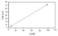
염화 하프늄 전구체로 도면 5a-5d에서 설명된 공정후에 2개의 산화 하프늄 박막은 100 Hf(NO3)4/HfCl4 싸이클 및 6 Hf(NO3)4/HfCl4 싸이클로 증착되었다. 어느 한 박막을 위한 증착 후 어닐링은 없었다. 산화 하프늄 박막은 170 ℃에서 약 10초의 펄스 길이로 증착되었다. 양 박막은 증착 단계 후에 시각적으로 균일하다. 또한, X-ray 반사성 측정은 부드럽고 균일한 증착된 박막을 지시하였다. 분광기 엘립소메트리 (ellipsometry) 측정은 100 Hf(NO3)4/HfCl4싸이클을 갖는 산화 하프늄이 굴절율 n0=1.80, n1=181, 및 n2=-0.70, 파장 λ=632.8에서 n=1.84 를 갖는 투명박막으로 모델링될 수 있음을 나타내었다. 또한, 분광기 엘립소메트리 측정은 100 Hf(NO3)4/HfCl4 싸이클을 갖는 산화 하프늄이 평균 두께 72.3 nm (±0.2 nm) 을 가지며 0.7 nm/싸이클 의 성장을 나타내고, 6 Hf(NO3)4/HfCl4 싸이클은 평균 두께 5.4 nm (±0.07 nm) 을 가지며 0.9 nm/싸이클을 나타내는 것을 의미한다. 이 증착율 범위는 Hf(NO3)4/H2O 또는 HfCl4/H2O 증착 중 어느 하나를 대해 이전에 보고된 것에 비해 대략 5내지 9배이다.Two hafnium oxide thin films were deposited with 100 Hf (NO3 )4 / HfCl4 cycles and 6 Hf (NO3 )4 / HfCl4 cycles after the process described in FIGS. 5A-5D with hafnium chloride precursors. There was no post deposition annealing for either thin film. Hafnium oxide thin films were deposited at 170 ° C. with a pulse length of about 10 seconds. Both thin films are visually uniform after the deposition step. In addition, X-ray reflectivity measurements indicated a smooth, uniform deposited thin film. Spectroscopy ellipsometry (ellipsometry) measurement is100 Hf (NO 3) 4 / HfCl 4 is hafnium oxide having a refractive index of the cyclen 0 = 1.80, n 1 = 181, and n2 = -0.70, at a wavelength λ = 632.8 n = It has been shown that it can be modeled as a transparent thin film having 1.84. In addition, spectroscopic ellipsometry measurements showed that hafnium oxide with 100 Hf (NO3 )4 / HfCl4 cycles had an average thickness of 72.3 nm (± 0.2 nm) and showed growth of 0.7 nm / cycle, 6 Hf (NO3 )4 / HfCl4 cycle means having an average thickness of 5.4 nm (± 0.07 nm) and representing 0.9 nm / cycle. This deposition rate range is approximately five to nine times that previously reported for either Hf (NO3 )4 / H2 O or HfCl4 / H2 O deposition.
도 10 은 본 발명 방법을 사용하여 증착된 산화 하프늄 박막을 위한 증착 두께 대 증착 싸이클의 플롯이다. 데이타 포인트를 연결한 곧은 점선은 음값에서 시간축을 통과하여, Hf(NO3)4/HfCl4 싸이클로 증착된 산화 하프늄 박막이 거의 즉시 증착됨을 의미한다. 높은 증착율, 증착된 박막들의 높은 균일성과 함께, 두께 대 싸이클 수의 상기 플롯은 Hf(NO3)4/H2O ADL에 정형적인 "배양" 싸이클이 본 발명 Hf(NO3)4/HfCl4 ADL 증착 방법으로 부터 제거됨을 암시한다.10 is a plot of deposition thickness versus deposition cycles for hafnium oxide thin films deposited using the method of the present invention. The straight dotted line connecting the data points means that the hafnium oxide thin film deposited with the Hf (NO3 )4 / HfCl4 cycle is deposited almost immediately across the time axis at negative values. With high deposition rate, high uniformity of deposited thin films, the plot of thickness versus cycle number shows that the "culture" cycles typical of Hf (NO3 )4 / H2 O ADL are the invention Hf (NO3 )4 / HfCl4. Imply removal from the ADL deposition method.
ALD 는 증착 기술의 순차적인 (sequential) 특징으로 인해, 나노층 박막을 증착하는데 적합한 방법이다. 산화 금속 나노층 증착을 위한 통상적인 ALD 방 법은, 제 1 금속 전구체 도입 (introducing), 그 후 제 1 산화 금속을 제공하기 위한 산화제의 도입, 그 후 제 2 금속 전구체의 도입, 및 그 후 제 2 산화 금속을 제공하기 위한 또다른 산화제 도입으로 된 (적절한 퍼징 단계 (purging steps) 를 갖는) 4 가지의 분리된 전구체 운반을 요구한다. 제 1 산화 금속 및 제 2 산화 금속은 함께 산화 금속 나노층 박막을 형성한다.ALD is a suitable method for depositing nanolayer thin films due to the sequential nature of the deposition technique. Conventional ALD methods for depositing metal oxide nanolayers include introducing a first metal precursor, then introducing an oxidant to provide a first metal oxide, then introducing a second metal precursor, and then It requires four separate precursor delivery (with proper purging steps) with another oxidant introduction to provide the metal dioxide. The first metal oxide and the second metal oxide together form a metal oxide nanolayer thin film.
본 발명은, 제 1 질산화 금속-함유 전구체의 도입 및 그 후 제 2 금속-함유 전구체 도입의 (적절한 퍼징 단계를 갖는) 단지 2 개의 별개의 전구체 운반만을 요구하는, 산화금속 나노층 증착을 위한 ALD 방법을 제공한다. 질산화 금속-함유 전구체는 제 2 금속에 대한 산화제로 작용하여, 나노층 박막의 산화 금속을 형성한다.The present invention requires only the introduction of the first metal oxynitride-containing precursor followed by the delivery of only two separate precursors (with the appropriate purging step) of the introduction of the second metal-containing precursor. An ALD method for metal nanolayer deposition is provided. The metal nitrate-containing precursor acts as an oxidant for the second metal, forming the metal oxide of the nanolayer thin film.
산화 단계를 제거함으로써, 본 발명은 증착 방법을 매우 단순화한다. 공정 시간 및 시스템 운반 복잡도는 거의 절반으로 삭감된다.By eliminating the oxidation step, the present invention greatly simplifies the deposition method. Process time and system transport complexity are cut in almost half.
또한, 별개의 산화 단계의 제거에 의해 산화 금속 혼합물을 더 잘 제어할 수 있고, 따라서 나노층 박막의 품질이 향상된다. 종전 기술 공정의 여분의 산화 단계는, 특히 질산염 전구체와 관련하여 풍부한 산소 때문에, 산화 금속을 산소-풍부 (oxygen-rich) 하게 만든다.
In addition, the removal of the separate oxidation step enables better control of the metal oxide mixture, thus improving the quality of the nanolayer thin film. The extra oxidation step of the prior art process makes the metal oxides oxygen-rich, especially due to the abundant oxygen associated with the nitrate precursors.
Claims (20)
Translated fromKoreanApplications Claiming Priority (2)
| Application Number | Priority Date | Filing Date | Title |
|---|---|---|---|
| US10/376,774US20040168627A1 (en) | 2003-02-27 | 2003-02-27 | Atomic layer deposition of oxide film |
| US10/376,774 | 2003-02-27 |
Publications (2)
| Publication Number | Publication Date |
|---|---|
| KR20040077570A KR20040077570A (en) | 2004-09-04 |
| KR100591508B1true KR100591508B1 (en) | 2006-06-19 |
Family
ID=32907993
Family Applications (1)
| Application Number | Title | Priority Date | Filing Date |
|---|---|---|---|
| KR1020040013705AExpired - Fee RelatedKR100591508B1 (en) | 2003-02-27 | 2004-02-27 | Atomic layer deposition of oxide film |
Country Status (4)
| Country | Link |
|---|---|
| US (1) | US20040168627A1 (en) |
| JP (1) | JP4293359B2 (en) |
| KR (1) | KR100591508B1 (en) |
| TW (1) | TWI263695B (en) |
Families Citing this family (457)
| Publication number | Priority date | Publication date | Assignee | Title |
|---|---|---|---|---|
| US6852167B2 (en) | 2001-03-01 | 2005-02-08 | Micron Technology, Inc. | Methods, systems, and apparatus for uniform chemical-vapor depositions |
| US8026161B2 (en) | 2001-08-30 | 2011-09-27 | Micron Technology, Inc. | Highly reliable amorphous high-K gate oxide ZrO2 |
| US7160577B2 (en) | 2002-05-02 | 2007-01-09 | Micron Technology, Inc. | Methods for atomic-layer deposition of aluminum oxides in integrated circuits |
| US7589029B2 (en) | 2002-05-02 | 2009-09-15 | Micron Technology, Inc. | Atomic layer deposition and conversion |
| US7221586B2 (en) | 2002-07-08 | 2007-05-22 | Micron Technology, Inc. | Memory utilizing oxide nanolaminates |
| US7192892B2 (en) | 2003-03-04 | 2007-03-20 | Micron Technology, Inc. | Atomic layer deposited dielectric layers |
| US7135369B2 (en) | 2003-03-31 | 2006-11-14 | Micron Technology, Inc. | Atomic layer deposited ZrAlxOy dielectric layers including Zr4AlO9 |
| US20050170665A1 (en)* | 2003-04-17 | 2005-08-04 | Fujitsu Limited | Method of forming a high dielectric film |
| US7183186B2 (en) | 2003-04-22 | 2007-02-27 | Micro Technology, Inc. | Atomic layer deposited ZrTiO4 films |
| US7192824B2 (en) | 2003-06-24 | 2007-03-20 | Micron Technology, Inc. | Lanthanide oxide / hafnium oxide dielectric layers |
| US8722160B2 (en)* | 2003-10-31 | 2014-05-13 | Aeris Capital Sustainable Ip Ltd. | Inorganic/organic hybrid nanolaminate barrier film |
| US7154779B2 (en)* | 2004-01-21 | 2006-12-26 | Sandisk Corporation | Non-volatile memory cell using high-k material inter-gate programming |
| US8323754B2 (en) | 2004-05-21 | 2012-12-04 | Applied Materials, Inc. | Stabilization of high-k dielectric materials |
| US6987063B2 (en)* | 2004-06-10 | 2006-01-17 | Freescale Semiconductor, Inc. | Method to reduce impurity elements during semiconductor film deposition |
| US7081421B2 (en) | 2004-08-26 | 2006-07-25 | Micron Technology, Inc. | Lanthanide oxide dielectric layer |
| US7588988B2 (en) | 2004-08-31 | 2009-09-15 | Micron Technology, Inc. | Method of forming apparatus having oxide films formed using atomic layer deposition |
| US7494939B2 (en) | 2004-08-31 | 2009-02-24 | Micron Technology, Inc. | Methods for forming a lanthanum-metal oxide dielectric layer |
| JP2006169556A (en)* | 2004-12-13 | 2006-06-29 | Horiba Ltd | Method for forming metal oxide thin film |
| US7235501B2 (en)* | 2004-12-13 | 2007-06-26 | Micron Technology, Inc. | Lanthanum hafnium oxide dielectrics |
| US7560395B2 (en) | 2005-01-05 | 2009-07-14 | Micron Technology, Inc. | Atomic layer deposited hafnium tantalum oxide dielectrics |
| US7316962B2 (en)* | 2005-01-07 | 2008-01-08 | Infineon Technologies Ag | High dielectric constant materials |
| US20060151822A1 (en)* | 2005-01-07 | 2006-07-13 | Shrinivas Govindarajan | DRAM with high K dielectric storage capacitor and method of making the same |
| US20060151845A1 (en)* | 2005-01-07 | 2006-07-13 | Shrinivas Govindarajan | Method to control interfacial properties for capacitors using a metal flash layer |
| US7508648B2 (en)* | 2005-02-08 | 2009-03-24 | Micron Technology, Inc. | Atomic layer deposition of Dy doped HfO2 films as gate dielectrics |
| US7498247B2 (en) | 2005-02-23 | 2009-03-03 | Micron Technology, Inc. | Atomic layer deposition of Hf3N4/HfO2 films as gate dielectrics |
| US7687409B2 (en) | 2005-03-29 | 2010-03-30 | Micron Technology, Inc. | Atomic layer deposited titanium silicon oxide films |
| US7662729B2 (en) | 2005-04-28 | 2010-02-16 | Micron Technology, Inc. | Atomic layer deposition of a ruthenium layer to a lanthanide oxide dielectric layer |
| US7390756B2 (en)* | 2005-04-28 | 2008-06-24 | Micron Technology, Inc. | Atomic layer deposited zirconium silicon oxide films |
| US7927948B2 (en) | 2005-07-20 | 2011-04-19 | Micron Technology, Inc. | Devices with nanocrystals and methods of formation |
| US7544596B2 (en) | 2005-08-30 | 2009-06-09 | Micron Technology, Inc. | Atomic layer deposition of GdScO3 films as gate dielectrics |
| US8110469B2 (en) | 2005-08-30 | 2012-02-07 | Micron Technology, Inc. | Graded dielectric layers |
| US20070059945A1 (en)* | 2005-09-12 | 2007-03-15 | Nima Mohklesi | Atomic layer deposition with nitridation and oxidation |
| JP5128289B2 (en)* | 2005-12-06 | 2013-01-23 | 株式会社トリケミカル研究所 | Hafnium-based compound, hafnium-based thin film forming material, and hafnium-based thin film forming method |
| US7592251B2 (en)* | 2005-12-08 | 2009-09-22 | Micron Technology, Inc. | Hafnium tantalum titanium oxide films |
| JP4745137B2 (en)* | 2006-06-02 | 2011-08-10 | 株式会社Adeka | Thin film forming raw material, thin film manufacturing method, and hafnium compound |
| US7605030B2 (en) | 2006-08-31 | 2009-10-20 | Micron Technology, Inc. | Hafnium tantalum oxynitride high-k dielectric and metal gates |
| US8986456B2 (en) | 2006-10-10 | 2015-03-24 | Asm America, Inc. | Precursor delivery system |
| KR100877100B1 (en)* | 2007-04-16 | 2009-01-09 | 주식회사 하이닉스반도체 | Nonvolatile Memory Device Manufacturing Method |
| US8076237B2 (en)* | 2008-05-09 | 2011-12-13 | Asm America, Inc. | Method and apparatus for 3D interconnect |
| US10378106B2 (en) | 2008-11-14 | 2019-08-13 | Asm Ip Holding B.V. | Method of forming insulation film by modified PEALD |
| US9394608B2 (en) | 2009-04-06 | 2016-07-19 | Asm America, Inc. | Semiconductor processing reactor and components thereof |
| US8071452B2 (en)* | 2009-04-27 | 2011-12-06 | Asm America, Inc. | Atomic layer deposition of hafnium lanthanum oxides |
| US20100290945A1 (en)* | 2009-05-13 | 2010-11-18 | Ce Ma | Solution based zirconium precursors for atomic layer deposition |
| US8877655B2 (en) | 2010-05-07 | 2014-11-04 | Asm America, Inc. | Systems and methods for thin-film deposition of metal oxides using excited nitrogen-oxygen species |
| US8883270B2 (en) | 2009-08-14 | 2014-11-11 | Asm America, Inc. | Systems and methods for thin-film deposition of metal oxides using excited nitrogen—oxygen species |
| US8802201B2 (en) | 2009-08-14 | 2014-08-12 | Asm America, Inc. | Systems and methods for thin-film deposition of metal oxides using excited nitrogen-oxygen species |
| US8771822B2 (en)* | 2011-01-18 | 2014-07-08 | Wisconsin Alumni Research Foundation | Methods for the growth of three-dimensional nanorod networks |
| US9312155B2 (en) | 2011-06-06 | 2016-04-12 | Asm Japan K.K. | High-throughput semiconductor-processing apparatus equipped with multiple dual-chamber modules |
| US9793148B2 (en) | 2011-06-22 | 2017-10-17 | Asm Japan K.K. | Method for positioning wafers in multiple wafer transport |
| US10364496B2 (en) | 2011-06-27 | 2019-07-30 | Asm Ip Holding B.V. | Dual section module having shared and unshared mass flow controllers |
| US10854498B2 (en) | 2011-07-15 | 2020-12-01 | Asm Ip Holding B.V. | Wafer-supporting device and method for producing same |
| US20130023129A1 (en) | 2011-07-20 | 2013-01-24 | Asm America, Inc. | Pressure transmitter for a semiconductor processing environment |
| US9096931B2 (en) | 2011-10-27 | 2015-08-04 | Asm America, Inc | Deposition valve assembly and method of heating the same |
| US9341296B2 (en) | 2011-10-27 | 2016-05-17 | Asm America, Inc. | Heater jacket for a fluid line |
| US9017481B1 (en) | 2011-10-28 | 2015-04-28 | Asm America, Inc. | Process feed management for semiconductor substrate processing |
| US9005539B2 (en) | 2011-11-23 | 2015-04-14 | Asm Ip Holding B.V. | Chamber sealing member |
| US9167625B2 (en) | 2011-11-23 | 2015-10-20 | Asm Ip Holding B.V. | Radiation shielding for a substrate holder |
| US9202727B2 (en) | 2012-03-02 | 2015-12-01 | ASM IP Holding | Susceptor heater shim |
| US8946830B2 (en) | 2012-04-04 | 2015-02-03 | Asm Ip Holdings B.V. | Metal oxide protective layer for a semiconductor device |
| TWI622664B (en) | 2012-05-02 | 2018-05-01 | Asm智慧財產控股公司 | Phase stable film, structure and device comprising the same, and method of forming same |
| US8728832B2 (en) | 2012-05-07 | 2014-05-20 | Asm Ip Holdings B.V. | Semiconductor device dielectric interface layer |
| US8933375B2 (en) | 2012-06-27 | 2015-01-13 | Asm Ip Holding B.V. | Susceptor heater and method of heating a substrate |
| US9558931B2 (en) | 2012-07-27 | 2017-01-31 | Asm Ip Holding B.V. | System and method for gas-phase sulfur passivation of a semiconductor surface |
| US9117866B2 (en) | 2012-07-31 | 2015-08-25 | Asm Ip Holding B.V. | Apparatus and method for calculating a wafer position in a processing chamber under process conditions |
| US9169975B2 (en) | 2012-08-28 | 2015-10-27 | Asm Ip Holding B.V. | Systems and methods for mass flow controller verification |
| US9659799B2 (en) | 2012-08-28 | 2017-05-23 | Asm Ip Holding B.V. | Systems and methods for dynamic semiconductor process scheduling |
| US9021985B2 (en) | 2012-09-12 | 2015-05-05 | Asm Ip Holdings B.V. | Process gas management for an inductively-coupled plasma deposition reactor |
| US9324811B2 (en) | 2012-09-26 | 2016-04-26 | Asm Ip Holding B.V. | Structures and devices including a tensile-stressed silicon arsenic layer and methods of forming same |
| US10714315B2 (en) | 2012-10-12 | 2020-07-14 | Asm Ip Holdings B.V. | Semiconductor reaction chamber showerhead |
| US9640416B2 (en) | 2012-12-26 | 2017-05-02 | Asm Ip Holding B.V. | Single-and dual-chamber module-attachable wafer-handling chamber |
| US8894870B2 (en) | 2013-02-01 | 2014-11-25 | Asm Ip Holding B.V. | Multi-step method and apparatus for etching compounds containing a metal |
| US20160376700A1 (en) | 2013-02-01 | 2016-12-29 | Asm Ip Holding B.V. | System for treatment of deposition reactor |
| US9589770B2 (en) | 2013-03-08 | 2017-03-07 | Asm Ip Holding B.V. | Method and systems for in-situ formation of intermediate reactive species |
| US9484191B2 (en) | 2013-03-08 | 2016-11-01 | Asm Ip Holding B.V. | Pulsed remote plasma method and system |
| US8993054B2 (en) | 2013-07-12 | 2015-03-31 | Asm Ip Holding B.V. | Method and system to reduce outgassing in a reaction chamber |
| US9018111B2 (en) | 2013-07-22 | 2015-04-28 | Asm Ip Holding B.V. | Semiconductor reaction chamber with plasma capabilities |
| US9793115B2 (en) | 2013-08-14 | 2017-10-17 | Asm Ip Holding B.V. | Structures and devices including germanium-tin films and methods of forming same |
| US9396934B2 (en) | 2013-08-14 | 2016-07-19 | Asm Ip Holding B.V. | Methods of forming films including germanium tin and structures and devices including the films |
| US9240412B2 (en) | 2013-09-27 | 2016-01-19 | Asm Ip Holding B.V. | Semiconductor structure and device and methods of forming same using selective epitaxial process |
| US9556516B2 (en) | 2013-10-09 | 2017-01-31 | ASM IP Holding B.V | Method for forming Ti-containing film by PEALD using TDMAT or TDEAT |
| US9605343B2 (en) | 2013-11-13 | 2017-03-28 | Asm Ip Holding B.V. | Method for forming conformal carbon films, structures conformal carbon film, and system of forming same |
| US10179947B2 (en) | 2013-11-26 | 2019-01-15 | Asm Ip Holding B.V. | Method for forming conformal nitrided, oxidized, or carbonized dielectric film by atomic layer deposition |
| US10683571B2 (en) | 2014-02-25 | 2020-06-16 | Asm Ip Holding B.V. | Gas supply manifold and method of supplying gases to chamber using same |
| US9447498B2 (en) | 2014-03-18 | 2016-09-20 | Asm Ip Holding B.V. | Method for performing uniform processing in gas system-sharing multiple reaction chambers |
| US10167557B2 (en) | 2014-03-18 | 2019-01-01 | Asm Ip Holding B.V. | Gas distribution system, reactor including the system, and methods of using the same |
| US11015245B2 (en) | 2014-03-19 | 2021-05-25 | Asm Ip Holding B.V. | Gas-phase reactor and system having exhaust plenum and components thereof |
| US9404587B2 (en) | 2014-04-24 | 2016-08-02 | ASM IP Holding B.V | Lockout tagout for semiconductor vacuum valve |
| US10858737B2 (en) | 2014-07-28 | 2020-12-08 | Asm Ip Holding B.V. | Showerhead assembly and components thereof |
| US9543180B2 (en) | 2014-08-01 | 2017-01-10 | Asm Ip Holding B.V. | Apparatus and method for transporting wafers between wafer carrier and process tool under vacuum |
| US9890456B2 (en) | 2014-08-21 | 2018-02-13 | Asm Ip Holding B.V. | Method and system for in situ formation of gas-phase compounds |
| US9657845B2 (en) | 2014-10-07 | 2017-05-23 | Asm Ip Holding B.V. | Variable conductance gas distribution apparatus and method |
| US10941490B2 (en) | 2014-10-07 | 2021-03-09 | Asm Ip Holding B.V. | Multiple temperature range susceptor, assembly, reactor and system including the susceptor, and methods of using the same |
| KR102300403B1 (en) | 2014-11-19 | 2021-09-09 | 에이에스엠 아이피 홀딩 비.브이. | Method of depositing thin film |
| KR102263121B1 (en) | 2014-12-22 | 2021-06-09 | 에이에스엠 아이피 홀딩 비.브이. | Semiconductor device and manufacuring method thereof |
| US9478415B2 (en) | 2015-02-13 | 2016-10-25 | Asm Ip Holding B.V. | Method for forming film having low resistance and shallow junction depth |
| US10529542B2 (en) | 2015-03-11 | 2020-01-07 | Asm Ip Holdings B.V. | Cross-flow reactor and method |
| US10276355B2 (en) | 2015-03-12 | 2019-04-30 | Asm Ip Holding B.V. | Multi-zone reactor, system including the reactor, and method of using the same |
| US10458018B2 (en) | 2015-06-26 | 2019-10-29 | Asm Ip Holding B.V. | Structures including metal carbide material, devices including the structures, and methods of forming same |
| US10600673B2 (en) | 2015-07-07 | 2020-03-24 | Asm Ip Holding B.V. | Magnetic susceptor to baseplate seal |
| US9899291B2 (en) | 2015-07-13 | 2018-02-20 | Asm Ip Holding B.V. | Method for protecting layer by forming hydrocarbon-based extremely thin film |
| US10043661B2 (en) | 2015-07-13 | 2018-08-07 | Asm Ip Holding B.V. | Method for protecting layer by forming hydrocarbon-based extremely thin film |
| US10083836B2 (en) | 2015-07-24 | 2018-09-25 | Asm Ip Holding B.V. | Formation of boron-doped titanium metal films with high work function |
| US10087525B2 (en) | 2015-08-04 | 2018-10-02 | Asm Ip Holding B.V. | Variable gap hard stop design |
| US9647114B2 (en) | 2015-08-14 | 2017-05-09 | Asm Ip Holding B.V. | Methods of forming highly p-type doped germanium tin films and structures and devices including the films |
| KR101752059B1 (en)* | 2015-08-24 | 2017-06-30 | 인천대학교 산학협력단 | Enhanced Electric Device for MOS Capacitor and Manufacturing Method thereof |
| US9711345B2 (en) | 2015-08-25 | 2017-07-18 | Asm Ip Holding B.V. | Method for forming aluminum nitride-based film by PEALD |
| US9960072B2 (en) | 2015-09-29 | 2018-05-01 | Asm Ip Holding B.V. | Variable adjustment for precise matching of multiple chamber cavity housings |
| US9909214B2 (en) | 2015-10-15 | 2018-03-06 | Asm Ip Holding B.V. | Method for depositing dielectric film in trenches by PEALD |
| US10211308B2 (en) | 2015-10-21 | 2019-02-19 | Asm Ip Holding B.V. | NbMC layers |
| US10322384B2 (en) | 2015-11-09 | 2019-06-18 | Asm Ip Holding B.V. | Counter flow mixer for process chamber |
| US9455138B1 (en) | 2015-11-10 | 2016-09-27 | Asm Ip Holding B.V. | Method for forming dielectric film in trenches by PEALD using H-containing gas |
| US9905420B2 (en) | 2015-12-01 | 2018-02-27 | Asm Ip Holding B.V. | Methods of forming silicon germanium tin films and structures and devices including the films |
| US9607837B1 (en) | 2015-12-21 | 2017-03-28 | Asm Ip Holding B.V. | Method for forming silicon oxide cap layer for solid state diffusion process |
| US9627221B1 (en) | 2015-12-28 | 2017-04-18 | Asm Ip Holding B.V. | Continuous process incorporating atomic layer etching |
| US9735024B2 (en) | 2015-12-28 | 2017-08-15 | Asm Ip Holding B.V. | Method of atomic layer etching using functional group-containing fluorocarbon |
| US11139308B2 (en) | 2015-12-29 | 2021-10-05 | Asm Ip Holding B.V. | Atomic layer deposition of III-V compounds to form V-NAND devices |
| US9754779B1 (en) | 2016-02-19 | 2017-09-05 | Asm Ip Holding B.V. | Method for forming silicon nitride film selectively on sidewalls or flat surfaces of trenches |
| US10468251B2 (en) | 2016-02-19 | 2019-11-05 | Asm Ip Holding B.V. | Method for forming spacers using silicon nitride film for spacer-defined multiple patterning |
| US10529554B2 (en) | 2016-02-19 | 2020-01-07 | Asm Ip Holding B.V. | Method for forming silicon nitride film selectively on sidewalls or flat surfaces of trenches |
| US9981286B2 (en)* | 2016-03-08 | 2018-05-29 | Asm Ip Holding B.V. | Selective formation of metal silicides |
| US10501866B2 (en) | 2016-03-09 | 2019-12-10 | Asm Ip Holding B.V. | Gas distribution apparatus for improved film uniformity in an epitaxial system |
| US10343920B2 (en) | 2016-03-18 | 2019-07-09 | Asm Ip Holding B.V. | Aligned carbon nanotubes |
| US9892913B2 (en) | 2016-03-24 | 2018-02-13 | Asm Ip Holding B.V. | Radial and thickness control via biased multi-port injection settings |
| US10865475B2 (en) | 2016-04-21 | 2020-12-15 | Asm Ip Holding B.V. | Deposition of metal borides and silicides |
| US10190213B2 (en) | 2016-04-21 | 2019-01-29 | Asm Ip Holding B.V. | Deposition of metal borides |
| US10087522B2 (en) | 2016-04-21 | 2018-10-02 | Asm Ip Holding B.V. | Deposition of metal borides |
| US10032628B2 (en) | 2016-05-02 | 2018-07-24 | Asm Ip Holding B.V. | Source/drain performance through conformal solid state doping |
| US10367080B2 (en) | 2016-05-02 | 2019-07-30 | Asm Ip Holding B.V. | Method of forming a germanium oxynitride film |
| KR102592471B1 (en) | 2016-05-17 | 2023-10-20 | 에이에스엠 아이피 홀딩 비.브이. | Method of forming metal interconnection and method of fabricating semiconductor device using the same |
| US11453943B2 (en) | 2016-05-25 | 2022-09-27 | Asm Ip Holding B.V. | Method for forming carbon-containing silicon/metal oxide or nitride film by ALD using silicon precursor and hydrocarbon precursor |
| US10388509B2 (en) | 2016-06-28 | 2019-08-20 | Asm Ip Holding B.V. | Formation of epitaxial layers via dislocation filtering |
| US9859151B1 (en) | 2016-07-08 | 2018-01-02 | Asm Ip Holding B.V. | Selective film deposition method to form air gaps |
| US10612137B2 (en) | 2016-07-08 | 2020-04-07 | Asm Ip Holdings B.V. | Organic reactants for atomic layer deposition |
| US9793135B1 (en) | 2016-07-14 | 2017-10-17 | ASM IP Holding B.V | Method of cyclic dry etching using etchant film |
| US10714385B2 (en) | 2016-07-19 | 2020-07-14 | Asm Ip Holding B.V. | Selective deposition of tungsten |
| KR102354490B1 (en) | 2016-07-27 | 2022-01-21 | 에이에스엠 아이피 홀딩 비.브이. | Method of processing a substrate |
| US10395919B2 (en) | 2016-07-28 | 2019-08-27 | Asm Ip Holding B.V. | Method and apparatus for filling a gap |
| US10177025B2 (en) | 2016-07-28 | 2019-01-08 | Asm Ip Holding B.V. | Method and apparatus for filling a gap |
| US9887082B1 (en) | 2016-07-28 | 2018-02-06 | Asm Ip Holding B.V. | Method and apparatus for filling a gap |
| US9812320B1 (en) | 2016-07-28 | 2017-11-07 | Asm Ip Holding B.V. | Method and apparatus for filling a gap |
| KR102532607B1 (en) | 2016-07-28 | 2023-05-15 | 에이에스엠 아이피 홀딩 비.브이. | Substrate processing apparatus and method of operating the same |
| US10090316B2 (en) | 2016-09-01 | 2018-10-02 | Asm Ip Holding B.V. | 3D stacked multilayer semiconductor memory using doped select transistor channel |
| US10410943B2 (en) | 2016-10-13 | 2019-09-10 | Asm Ip Holding B.V. | Method for passivating a surface of a semiconductor and related systems |
| US10643826B2 (en) | 2016-10-26 | 2020-05-05 | Asm Ip Holdings B.V. | Methods for thermally calibrating reaction chambers |
| US11532757B2 (en) | 2016-10-27 | 2022-12-20 | Asm Ip Holding B.V. | Deposition of charge trapping layers |
| US10435790B2 (en) | 2016-11-01 | 2019-10-08 | Asm Ip Holding B.V. | Method of subatmospheric plasma-enhanced ALD using capacitively coupled electrodes with narrow gap |
| US10714350B2 (en) | 2016-11-01 | 2020-07-14 | ASM IP Holdings, B.V. | Methods for forming a transition metal niobium nitride film on a substrate by atomic layer deposition and related semiconductor device structures |
| US10229833B2 (en) | 2016-11-01 | 2019-03-12 | Asm Ip Holding B.V. | Methods for forming a transition metal nitride film on a substrate by atomic layer deposition and related semiconductor device structures |
| US10643904B2 (en) | 2016-11-01 | 2020-05-05 | Asm Ip Holdings B.V. | Methods for forming a semiconductor device and related semiconductor device structures |
| US10134757B2 (en) | 2016-11-07 | 2018-11-20 | Asm Ip Holding B.V. | Method of processing a substrate and a device manufactured by using the method |
| KR102546317B1 (en) | 2016-11-15 | 2023-06-21 | 에이에스엠 아이피 홀딩 비.브이. | Gas supply unit and substrate processing apparatus including the same |
| US10340135B2 (en) | 2016-11-28 | 2019-07-02 | Asm Ip Holding B.V. | Method of topologically restricted plasma-enhanced cyclic deposition of silicon or metal nitride |
| KR102762543B1 (en) | 2016-12-14 | 2025-02-05 | 에이에스엠 아이피 홀딩 비.브이. | Substrate processing apparatus |
| US9916980B1 (en) | 2016-12-15 | 2018-03-13 | Asm Ip Holding B.V. | Method of forming a structure on a substrate |
| US11447861B2 (en) | 2016-12-15 | 2022-09-20 | Asm Ip Holding B.V. | Sequential infiltration synthesis apparatus and a method of forming a patterned structure |
| US11581186B2 (en) | 2016-12-15 | 2023-02-14 | Asm Ip Holding B.V. | Sequential infiltration synthesis apparatus |
| KR102700194B1 (en) | 2016-12-19 | 2024-08-28 | 에이에스엠 아이피 홀딩 비.브이. | Substrate processing apparatus |
| US10269558B2 (en) | 2016-12-22 | 2019-04-23 | Asm Ip Holding B.V. | Method of forming a structure on a substrate |
| US10867788B2 (en) | 2016-12-28 | 2020-12-15 | Asm Ip Holding B.V. | Method of forming a structure on a substrate |
| US11390950B2 (en) | 2017-01-10 | 2022-07-19 | Asm Ip Holding B.V. | Reactor system and method to reduce residue buildup during a film deposition process |
| US10655221B2 (en) | 2017-02-09 | 2020-05-19 | Asm Ip Holding B.V. | Method for depositing oxide film by thermal ALD and PEALD |
| US10468261B2 (en) | 2017-02-15 | 2019-11-05 | Asm Ip Holding B.V. | Methods for forming a metallic film on a substrate by cyclical deposition and related semiconductor device structures |
| US10283353B2 (en) | 2017-03-29 | 2019-05-07 | Asm Ip Holding B.V. | Method of reforming insulating film deposited on substrate with recess pattern |
| US10529563B2 (en) | 2017-03-29 | 2020-01-07 | Asm Ip Holdings B.V. | Method for forming doped metal oxide films on a substrate by cyclical deposition and related semiconductor device structures |
| US10103040B1 (en) | 2017-03-31 | 2018-10-16 | Asm Ip Holding B.V. | Apparatus and method for manufacturing a semiconductor device |
| USD830981S1 (en) | 2017-04-07 | 2018-10-16 | Asm Ip Holding B.V. | Susceptor for semiconductor substrate processing apparatus |
| KR102457289B1 (en) | 2017-04-25 | 2022-10-21 | 에이에스엠 아이피 홀딩 비.브이. | Method for depositing a thin film and manufacturing a semiconductor device |
| US10892156B2 (en) | 2017-05-08 | 2021-01-12 | Asm Ip Holding B.V. | Methods for forming a silicon nitride film on a substrate and related semiconductor device structures |
| US10770286B2 (en) | 2017-05-08 | 2020-09-08 | Asm Ip Holdings B.V. | Methods for selectively forming a silicon nitride film on a substrate and related semiconductor device structures |
| US10446393B2 (en) | 2017-05-08 | 2019-10-15 | Asm Ip Holding B.V. | Methods for forming silicon-containing epitaxial layers and related semiconductor device structures |
| US10504742B2 (en) | 2017-05-31 | 2019-12-10 | Asm Ip Holding B.V. | Method of atomic layer etching using hydrogen plasma |
| US10886123B2 (en) | 2017-06-02 | 2021-01-05 | Asm Ip Holding B.V. | Methods for forming low temperature semiconductor layers and related semiconductor device structures |
| US10121652B1 (en)* | 2017-06-07 | 2018-11-06 | Nxp Usa, Inc. | Formation of metal oxide layer |
| US12040200B2 (en) | 2017-06-20 | 2024-07-16 | Asm Ip Holding B.V. | Semiconductor processing apparatus and methods for calibrating a semiconductor processing apparatus |
| US11306395B2 (en) | 2017-06-28 | 2022-04-19 | Asm Ip Holding B.V. | Methods for depositing a transition metal nitride film on a substrate by atomic layer deposition and related deposition apparatus |
| US10685834B2 (en) | 2017-07-05 | 2020-06-16 | Asm Ip Holdings B.V. | Methods for forming a silicon germanium tin layer and related semiconductor device structures |
| KR20190009245A (en) | 2017-07-18 | 2019-01-28 | 에이에스엠 아이피 홀딩 비.브이. | Methods for forming a semiconductor device structure and related semiconductor device structures |
| US11018002B2 (en) | 2017-07-19 | 2021-05-25 | Asm Ip Holding B.V. | Method for selectively depositing a Group IV semiconductor and related semiconductor device structures |
| US11374112B2 (en) | 2017-07-19 | 2022-06-28 | Asm Ip Holding B.V. | Method for depositing a group IV semiconductor and related semiconductor device structures |
| US10541333B2 (en) | 2017-07-19 | 2020-01-21 | Asm Ip Holding B.V. | Method for depositing a group IV semiconductor and related semiconductor device structures |
| US10312055B2 (en) | 2017-07-26 | 2019-06-04 | Asm Ip Holding B.V. | Method of depositing film by PEALD using negative bias |
| US10590535B2 (en) | 2017-07-26 | 2020-03-17 | Asm Ip Holdings B.V. | Chemical treatment, deposition and/or infiltration apparatus and method for using the same |
| US10605530B2 (en) | 2017-07-26 | 2020-03-31 | Asm Ip Holding B.V. | Assembly of a liner and a flange for a vertical furnace as well as the liner and the vertical furnace |
| TWI815813B (en) | 2017-08-04 | 2023-09-21 | 荷蘭商Asm智慧財產控股公司 | Showerhead assembly for distributing a gas within a reaction chamber |
| US10770336B2 (en) | 2017-08-08 | 2020-09-08 | Asm Ip Holding B.V. | Substrate lift mechanism and reactor including same |
| US10692741B2 (en) | 2017-08-08 | 2020-06-23 | Asm Ip Holdings B.V. | Radiation shield |
| US11139191B2 (en) | 2017-08-09 | 2021-10-05 | Asm Ip Holding B.V. | Storage apparatus for storing cassettes for substrates and processing apparatus equipped therewith |
| US10249524B2 (en) | 2017-08-09 | 2019-04-02 | Asm Ip Holding B.V. | Cassette holder assembly for a substrate cassette and holding member for use in such assembly |
| US11769682B2 (en) | 2017-08-09 | 2023-09-26 | Asm Ip Holding B.V. | Storage apparatus for storing cassettes for substrates and processing apparatus equipped therewith |
| US10236177B1 (en) | 2017-08-22 | 2019-03-19 | ASM IP Holding B.V.. | Methods for depositing a doped germanium tin semiconductor and related semiconductor device structures |
| USD900036S1 (en) | 2017-08-24 | 2020-10-27 | Asm Ip Holding B.V. | Heater electrical connector and adapter |
| US11830730B2 (en) | 2017-08-29 | 2023-11-28 | Asm Ip Holding B.V. | Layer forming method and apparatus |
| US11295980B2 (en) | 2017-08-30 | 2022-04-05 | Asm Ip Holding B.V. | Methods for depositing a molybdenum metal film over a dielectric surface of a substrate by a cyclical deposition process and related semiconductor device structures |
| US11056344B2 (en) | 2017-08-30 | 2021-07-06 | Asm Ip Holding B.V. | Layer forming method |
| TWI839906B (en)* | 2017-08-30 | 2024-04-21 | 荷蘭商Asm Ip私人控股有限公司 | Layer forming method |
| KR102491945B1 (en) | 2017-08-30 | 2023-01-26 | 에이에스엠 아이피 홀딩 비.브이. | Substrate processing apparatus |
| KR102401446B1 (en) | 2017-08-31 | 2022-05-24 | 에이에스엠 아이피 홀딩 비.브이. | Substrate processing apparatus |
| US10607895B2 (en) | 2017-09-18 | 2020-03-31 | Asm Ip Holdings B.V. | Method for forming a semiconductor device structure comprising a gate fill metal |
| KR102630301B1 (en) | 2017-09-21 | 2024-01-29 | 에이에스엠 아이피 홀딩 비.브이. | Method of sequential infiltration synthesis treatment of infiltrateable material and structures and devices formed using same |
| US10844484B2 (en) | 2017-09-22 | 2020-11-24 | Asm Ip Holding B.V. | Apparatus for dispensing a vapor phase reactant to a reaction chamber and related methods |
| KR102385386B1 (en)* | 2017-09-26 | 2022-04-11 | 어플라이드 머티어리얼스, 인코포레이티드 | Methods, materials and processes for native oxide removal and regrowth of dielectric oxides for better biosensor performance |
| US10658205B2 (en) | 2017-09-28 | 2020-05-19 | Asm Ip Holdings B.V. | Chemical dispensing apparatus and methods for dispensing a chemical to a reaction chamber |
| US10403504B2 (en) | 2017-10-05 | 2019-09-03 | Asm Ip Holding B.V. | Method for selectively depositing a metallic film on a substrate |
| US10319588B2 (en) | 2017-10-10 | 2019-06-11 | Asm Ip Holding B.V. | Method for depositing a metal chalcogenide on a substrate by cyclical deposition |
| US10923344B2 (en) | 2017-10-30 | 2021-02-16 | Asm Ip Holding B.V. | Methods for forming a semiconductor structure and related semiconductor structures |
| KR102443047B1 (en) | 2017-11-16 | 2022-09-14 | 에이에스엠 아이피 홀딩 비.브이. | Method of processing a substrate and a device manufactured by the same |
| US10910262B2 (en) | 2017-11-16 | 2021-02-02 | Asm Ip Holding B.V. | Method of selectively depositing a capping layer structure on a semiconductor device structure |
| US11022879B2 (en) | 2017-11-24 | 2021-06-01 | Asm Ip Holding B.V. | Method of forming an enhanced unexposed photoresist layer |
| CN111344522B (en) | 2017-11-27 | 2022-04-12 | 阿斯莫Ip控股公司 | Including clean mini-environment device |
| WO2019103613A1 (en) | 2017-11-27 | 2019-05-31 | Asm Ip Holding B.V. | A storage device for storing wafer cassettes for use with a batch furnace |
| US10290508B1 (en) | 2017-12-05 | 2019-05-14 | Asm Ip Holding B.V. | Method for forming vertical spacers for spacer-defined patterning |
| US10872771B2 (en) | 2018-01-16 | 2020-12-22 | Asm Ip Holding B. V. | Method for depositing a material film on a substrate within a reaction chamber by a cyclical deposition process and related device structures |
| TWI799494B (en) | 2018-01-19 | 2023-04-21 | 荷蘭商Asm 智慧財產控股公司 | Deposition method |
| KR102695659B1 (en) | 2018-01-19 | 2024-08-14 | 에이에스엠 아이피 홀딩 비.브이. | Method for depositing a gap filling layer by plasma assisted deposition |
| USD903477S1 (en) | 2018-01-24 | 2020-12-01 | Asm Ip Holdings B.V. | Metal clamp |
| US11018047B2 (en) | 2018-01-25 | 2021-05-25 | Asm Ip Holding B.V. | Hybrid lift pin |
| US10535516B2 (en) | 2018-02-01 | 2020-01-14 | Asm Ip Holdings B.V. | Method for depositing a semiconductor structure on a surface of a substrate and related semiconductor structures |
| USD880437S1 (en) | 2018-02-01 | 2020-04-07 | Asm Ip Holding B.V. | Gas supply plate for semiconductor manufacturing apparatus |
| US11081345B2 (en) | 2018-02-06 | 2021-08-03 | Asm Ip Holding B.V. | Method of post-deposition treatment for silicon oxide film |
| WO2019158960A1 (en) | 2018-02-14 | 2019-08-22 | Asm Ip Holding B.V. | A method for depositing a ruthenium-containing film on a substrate by a cyclical deposition process |
| US10896820B2 (en) | 2018-02-14 | 2021-01-19 | Asm Ip Holding B.V. | Method for depositing a ruthenium-containing film on a substrate by a cyclical deposition process |
| US10731249B2 (en) | 2018-02-15 | 2020-08-04 | Asm Ip Holding B.V. | Method of forming a transition metal containing film on a substrate by a cyclical deposition process, a method for supplying a transition metal halide compound to a reaction chamber, and related vapor deposition apparatus |
| KR102636427B1 (en) | 2018-02-20 | 2024-02-13 | 에이에스엠 아이피 홀딩 비.브이. | Substrate processing method and apparatus |
| US10658181B2 (en) | 2018-02-20 | 2020-05-19 | Asm Ip Holding B.V. | Method of spacer-defined direct patterning in semiconductor fabrication |
| US10975470B2 (en) | 2018-02-23 | 2021-04-13 | Asm Ip Holding B.V. | Apparatus for detecting or monitoring for a chemical precursor in a high temperature environment |
| US11473195B2 (en) | 2018-03-01 | 2022-10-18 | Asm Ip Holding B.V. | Semiconductor processing apparatus and a method for processing a substrate |
| US11629406B2 (en) | 2018-03-09 | 2023-04-18 | Asm Ip Holding B.V. | Semiconductor processing apparatus comprising one or more pyrometers for measuring a temperature of a substrate during transfer of the substrate |
| US11114283B2 (en) | 2018-03-16 | 2021-09-07 | Asm Ip Holding B.V. | Reactor, system including the reactor, and methods of manufacturing and using same |
| KR102646467B1 (en) | 2018-03-27 | 2024-03-11 | 에이에스엠 아이피 홀딩 비.브이. | Method of forming an electrode on a substrate and a semiconductor device structure including an electrode |
| US11088002B2 (en) | 2018-03-29 | 2021-08-10 | Asm Ip Holding B.V. | Substrate rack and a substrate processing system and method |
| US11230766B2 (en) | 2018-03-29 | 2022-01-25 | Asm Ip Holding B.V. | Substrate processing apparatus and method |
| US10510536B2 (en) | 2018-03-29 | 2019-12-17 | Asm Ip Holding B.V. | Method of depositing a co-doped polysilicon film on a surface of a substrate within a reaction chamber |
| KR102501472B1 (en) | 2018-03-30 | 2023-02-20 | 에이에스엠 아이피 홀딩 비.브이. | Substrate processing method |
| KR102600229B1 (en) | 2018-04-09 | 2023-11-10 | 에이에스엠 아이피 홀딩 비.브이. | Substrate supporting device, substrate processing apparatus including the same and substrate processing method |
| TWI811348B (en) | 2018-05-08 | 2023-08-11 | 荷蘭商Asm 智慧財產控股公司 | Methods for depositing an oxide film on a substrate by a cyclical deposition process and related device structures |
| US12025484B2 (en) | 2018-05-08 | 2024-07-02 | Asm Ip Holding B.V. | Thin film forming method |
| US12272527B2 (en) | 2018-05-09 | 2025-04-08 | Asm Ip Holding B.V. | Apparatus for use with hydrogen radicals and method of using same |
| KR20190129718A (en) | 2018-05-11 | 2019-11-20 | 에이에스엠 아이피 홀딩 비.브이. | Methods for forming a doped metal carbide film on a substrate and related semiconductor device structures |
| KR102079177B1 (en) | 2018-05-18 | 2020-02-19 | 서울대학교산학협력단 | Method for forming hafnium oxynitride film and semiconductor device using the same |
| KR102596988B1 (en) | 2018-05-28 | 2023-10-31 | 에이에스엠 아이피 홀딩 비.브이. | Method of processing a substrate and a device manufactured by the same |
| TWI840362B (en) | 2018-06-04 | 2024-05-01 | 荷蘭商Asm Ip私人控股有限公司 | Wafer handling chamber with moisture reduction |
| US11718913B2 (en) | 2018-06-04 | 2023-08-08 | Asm Ip Holding B.V. | Gas distribution system and reactor system including same |
| US11286562B2 (en) | 2018-06-08 | 2022-03-29 | Asm Ip Holding B.V. | Gas-phase chemical reactor and method of using same |
| KR102568797B1 (en) | 2018-06-21 | 2023-08-21 | 에이에스엠 아이피 홀딩 비.브이. | Substrate processing system |
| US10797133B2 (en) | 2018-06-21 | 2020-10-06 | Asm Ip Holding B.V. | Method for depositing a phosphorus doped silicon arsenide film and related semiconductor device structures |
| KR102854019B1 (en) | 2018-06-27 | 2025-09-02 | 에이에스엠 아이피 홀딩 비.브이. | Periodic deposition method for forming a metal-containing material and films and structures comprising the metal-containing material |
| TWI873894B (en) | 2018-06-27 | 2025-02-21 | 荷蘭商Asm Ip私人控股有限公司 | Cyclic deposition methods for forming metal-containing material and films and structures including the metal-containing material |
| KR102686758B1 (en) | 2018-06-29 | 2024-07-18 | 에이에스엠 아이피 홀딩 비.브이. | Method for depositing a thin film and manufacturing a semiconductor device |
| US10612136B2 (en) | 2018-06-29 | 2020-04-07 | ASM IP Holding, B.V. | Temperature-controlled flange and reactor system including same |
| US10755922B2 (en) | 2018-07-03 | 2020-08-25 | Asm Ip Holding B.V. | Method for depositing silicon-free carbon-containing film as gap-fill layer by pulse plasma-assisted deposition |
| US10388513B1 (en) | 2018-07-03 | 2019-08-20 | Asm Ip Holding B.V. | Method for depositing silicon-free carbon-containing film as gap-fill layer by pulse plasma-assisted deposition |
| US10767789B2 (en) | 2018-07-16 | 2020-09-08 | Asm Ip Holding B.V. | Diaphragm valves, valve components, and methods for forming valve components |
| US10483099B1 (en) | 2018-07-26 | 2019-11-19 | Asm Ip Holding B.V. | Method for forming thermally stable organosilicon polymer film |
| US11053591B2 (en) | 2018-08-06 | 2021-07-06 | Asm Ip Holding B.V. | Multi-port gas injection system and reactor system including same |
| US10883175B2 (en) | 2018-08-09 | 2021-01-05 | Asm Ip Holding B.V. | Vertical furnace for processing substrates and a liner for use therein |
| US10829852B2 (en) | 2018-08-16 | 2020-11-10 | Asm Ip Holding B.V. | Gas distribution device for a wafer processing apparatus |
| US11430674B2 (en) | 2018-08-22 | 2022-08-30 | Asm Ip Holding B.V. | Sensor array, apparatus for dispensing a vapor phase reactant to a reaction chamber and related methods |
| US11024523B2 (en) | 2018-09-11 | 2021-06-01 | Asm Ip Holding B.V. | Substrate processing apparatus and method |
| KR102707956B1 (en) | 2018-09-11 | 2024-09-19 | 에이에스엠 아이피 홀딩 비.브이. | Method for deposition of a thin film |
| US11049751B2 (en) | 2018-09-14 | 2021-06-29 | Asm Ip Holding B.V. | Cassette supply system to store and handle cassettes and processing apparatus equipped therewith |
| CN110970344B (en) | 2018-10-01 | 2024-10-25 | Asmip控股有限公司 | Substrate holding apparatus, system comprising the same and method of using the same |
| US11232963B2 (en) | 2018-10-03 | 2022-01-25 | Asm Ip Holding B.V. | Substrate processing apparatus and method |
| KR102592699B1 (en) | 2018-10-08 | 2023-10-23 | 에이에스엠 아이피 홀딩 비.브이. | Substrate support unit and apparatuses for depositing thin film and processing the substrate including the same |
| US10847365B2 (en) | 2018-10-11 | 2020-11-24 | Asm Ip Holding B.V. | Method of forming conformal silicon carbide film by cyclic CVD |
| US10811256B2 (en) | 2018-10-16 | 2020-10-20 | Asm Ip Holding B.V. | Method for etching a carbon-containing feature |
| KR102546322B1 (en) | 2018-10-19 | 2023-06-21 | 에이에스엠 아이피 홀딩 비.브이. | Substrate processing apparatus and substrate processing method |
| KR102605121B1 (en) | 2018-10-19 | 2023-11-23 | 에이에스엠 아이피 홀딩 비.브이. | Substrate processing apparatus and substrate processing method |
| USD948463S1 (en) | 2018-10-24 | 2022-04-12 | Asm Ip Holding B.V. | Susceptor for semiconductor substrate supporting apparatus |
| US10381219B1 (en) | 2018-10-25 | 2019-08-13 | Asm Ip Holding B.V. | Methods for forming a silicon nitride film |
| US12378665B2 (en) | 2018-10-26 | 2025-08-05 | Asm Ip Holding B.V. | High temperature coatings for a preclean and etch apparatus and related methods |
| US11087997B2 (en) | 2018-10-31 | 2021-08-10 | Asm Ip Holding B.V. | Substrate processing apparatus for processing substrates |
| KR102748291B1 (en) | 2018-11-02 | 2024-12-31 | 에이에스엠 아이피 홀딩 비.브이. | Substrate support unit and substrate processing apparatus including the same |
| US11572620B2 (en) | 2018-11-06 | 2023-02-07 | Asm Ip Holding B.V. | Methods for selectively depositing an amorphous silicon film on a substrate |
| US11031242B2 (en) | 2018-11-07 | 2021-06-08 | Asm Ip Holding B.V. | Methods for depositing a boron doped silicon germanium film |
| US10847366B2 (en) | 2018-11-16 | 2020-11-24 | Asm Ip Holding B.V. | Methods for depositing a transition metal chalcogenide film on a substrate by a cyclical deposition process |
| US10818758B2 (en) | 2018-11-16 | 2020-10-27 | Asm Ip Holding B.V. | Methods for forming a metal silicate film on a substrate in a reaction chamber and related semiconductor device structures |
| US10559458B1 (en) | 2018-11-26 | 2020-02-11 | Asm Ip Holding B.V. | Method of forming oxynitride film |
| US12040199B2 (en) | 2018-11-28 | 2024-07-16 | Asm Ip Holding B.V. | Substrate processing apparatus for processing substrates |
| US11217444B2 (en) | 2018-11-30 | 2022-01-04 | Asm Ip Holding B.V. | Method for forming an ultraviolet radiation responsive metal oxide-containing film |
| KR102636428B1 (en) | 2018-12-04 | 2024-02-13 | 에이에스엠 아이피 홀딩 비.브이. | A method for cleaning a substrate processing apparatus |
| US11158513B2 (en) | 2018-12-13 | 2021-10-26 | Asm Ip Holding B.V. | Methods for forming a rhenium-containing film on a substrate by a cyclical deposition process and related semiconductor device structures |
| TWI874340B (en) | 2018-12-14 | 2025-03-01 | 荷蘭商Asm Ip私人控股有限公司 | Method of forming device structure, structure formed by the method and system for performing the method |
| TWI866480B (en) | 2019-01-17 | 2024-12-11 | 荷蘭商Asm Ip 私人控股有限公司 | Methods of forming a transition metal containing film on a substrate by a cyclical deposition process |
| KR102727227B1 (en) | 2019-01-22 | 2024-11-07 | 에이에스엠 아이피 홀딩 비.브이. | Semiconductor processing device |
| CN111524788B (en) | 2019-02-01 | 2023-11-24 | Asm Ip私人控股有限公司 | Method for forming topologically selective films of silicon oxide |
| TWI845607B (en) | 2019-02-20 | 2024-06-21 | 荷蘭商Asm Ip私人控股有限公司 | Cyclical deposition method and apparatus for filling a recess formed within a substrate surface |
| TWI838458B (en) | 2019-02-20 | 2024-04-11 | 荷蘭商Asm Ip私人控股有限公司 | Apparatus and methods for plug fill deposition in 3-d nand applications |
| KR102626263B1 (en) | 2019-02-20 | 2024-01-16 | 에이에스엠 아이피 홀딩 비.브이. | Cyclical deposition method including treatment step and apparatus for same |
| TWI873122B (en) | 2019-02-20 | 2025-02-21 | 荷蘭商Asm Ip私人控股有限公司 | Method of filling a recess formed within a surface of a substrate, semiconductor structure formed according to the method, and semiconductor processing apparatus |
| TWI842826B (en) | 2019-02-22 | 2024-05-21 | 荷蘭商Asm Ip私人控股有限公司 | Substrate processing apparatus and method for processing substrate |
| KR102782593B1 (en) | 2019-03-08 | 2025-03-14 | 에이에스엠 아이피 홀딩 비.브이. | Structure Including SiOC Layer and Method of Forming Same |
| KR102858005B1 (en) | 2019-03-08 | 2025-09-09 | 에이에스엠 아이피 홀딩 비.브이. | Method for Selective Deposition of Silicon Nitride Layer and Structure Including Selectively-Deposited Silicon Nitride Layer |
| US11742198B2 (en) | 2019-03-08 | 2023-08-29 | Asm Ip Holding B.V. | Structure including SiOCN layer and method of forming same |
| JP2020167398A (en) | 2019-03-28 | 2020-10-08 | エーエスエム・アイピー・ホールディング・ベー・フェー | Door openers and substrate processing equipment provided with door openers |
| KR102809999B1 (en) | 2019-04-01 | 2025-05-19 | 에이에스엠 아이피 홀딩 비.브이. | Method of manufacturing semiconductor device |
| KR20200123380A (en) | 2019-04-19 | 2020-10-29 | 에이에스엠 아이피 홀딩 비.브이. | Layer forming method and apparatus |
| KR20200125453A (en) | 2019-04-24 | 2020-11-04 | 에이에스엠 아이피 홀딩 비.브이. | Gas-phase reactor system and method of using same |
| KR20200130121A (en) | 2019-05-07 | 2020-11-18 | 에이에스엠 아이피 홀딩 비.브이. | Chemical source vessel with dip tube |
| US11289326B2 (en) | 2019-05-07 | 2022-03-29 | Asm Ip Holding B.V. | Method for reforming amorphous carbon polymer film |
| KR20200130652A (en) | 2019-05-10 | 2020-11-19 | 에이에스엠 아이피 홀딩 비.브이. | Method of depositing material onto a surface and structure formed according to the method |
| JP7598201B2 (en) | 2019-05-16 | 2024-12-11 | エーエスエム・アイピー・ホールディング・ベー・フェー | Wafer boat handling apparatus, vertical batch furnace and method |
| JP7612342B2 (en) | 2019-05-16 | 2025-01-14 | エーエスエム・アイピー・ホールディング・ベー・フェー | Wafer boat handling apparatus, vertical batch furnace and method |
| USD947913S1 (en) | 2019-05-17 | 2022-04-05 | Asm Ip Holding B.V. | Susceptor shaft |
| USD975665S1 (en) | 2019-05-17 | 2023-01-17 | Asm Ip Holding B.V. | Susceptor shaft |
| USD935572S1 (en) | 2019-05-24 | 2021-11-09 | Asm Ip Holding B.V. | Gas channel plate |
| USD922229S1 (en) | 2019-06-05 | 2021-06-15 | Asm Ip Holding B.V. | Device for controlling a temperature of a gas supply unit |
| KR20200141002A (en) | 2019-06-06 | 2020-12-17 | 에이에스엠 아이피 홀딩 비.브이. | Method of using a gas-phase reactor system including analyzing exhausted gas |
| KR20200141931A (en) | 2019-06-10 | 2020-12-21 | 에이에스엠 아이피 홀딩 비.브이. | Method for cleaning quartz epitaxial chambers |
| KR20200143254A (en) | 2019-06-11 | 2020-12-23 | 에이에스엠 아이피 홀딩 비.브이. | Method of forming an electronic structure using an reforming gas, system for performing the method, and structure formed using the method |
| USD944946S1 (en) | 2019-06-14 | 2022-03-01 | Asm Ip Holding B.V. | Shower plate |
| US12082395B2 (en) | 2019-06-14 | 2024-09-03 | Samsung Electronics Co., Ltd. | Semiconductor memory devices and methods of fabricating the same |
| KR102795716B1 (en) | 2019-06-14 | 2025-04-15 | 삼성전자주식회사 | Semiconductor memory device and method of fabricating the same |
| USD931978S1 (en) | 2019-06-27 | 2021-09-28 | Asm Ip Holding B.V. | Showerhead vacuum transport |
| KR20210005515A (en) | 2019-07-03 | 2021-01-14 | 에이에스엠 아이피 홀딩 비.브이. | Temperature control assembly for substrate processing apparatus and method of using same |
| JP7499079B2 (en) | 2019-07-09 | 2024-06-13 | エーエスエム・アイピー・ホールディング・ベー・フェー | Plasma device using coaxial waveguide and substrate processing method |
| CN112216646A (en) | 2019-07-10 | 2021-01-12 | Asm Ip私人控股有限公司 | Substrate supporting assembly and substrate processing device comprising same |
| KR20210010307A (en) | 2019-07-16 | 2021-01-27 | 에이에스엠 아이피 홀딩 비.브이. | Substrate processing apparatus |
| KR20210010816A (en) | 2019-07-17 | 2021-01-28 | 에이에스엠 아이피 홀딩 비.브이. | Radical assist ignition plasma system and method |
| US11462398B2 (en)* | 2019-07-17 | 2022-10-04 | International Business Machines Corporation | Ligand selection for ternary oxide thin films |
| KR102860110B1 (en) | 2019-07-17 | 2025-09-16 | 에이에스엠 아이피 홀딩 비.브이. | Methods of forming silicon germanium structures |
| US11643724B2 (en) | 2019-07-18 | 2023-05-09 | Asm Ip Holding B.V. | Method of forming structures using a neutral beam |
| KR20210010817A (en) | 2019-07-19 | 2021-01-28 | 에이에스엠 아이피 홀딩 비.브이. | Method of Forming Topology-Controlled Amorphous Carbon Polymer Film |
| TWI839544B (en) | 2019-07-19 | 2024-04-21 | 荷蘭商Asm Ip私人控股有限公司 | Method of forming topology-controlled amorphous carbon polymer film |
| US11081343B2 (en) | 2019-07-19 | 2021-08-03 | International Business Machines Corporation | Sub-stoichiometric metal-oxide thin films |
| TWI851767B (en) | 2019-07-29 | 2024-08-11 | 荷蘭商Asm Ip私人控股有限公司 | Methods for selective deposition utilizing n-type dopants and/or alternative dopants to achieve high dopant incorporation |
| CN112309900A (en) | 2019-07-30 | 2021-02-02 | Asm Ip私人控股有限公司 | Substrate processing apparatus |
| CN112309899A (en) | 2019-07-30 | 2021-02-02 | Asm Ip私人控股有限公司 | Substrate processing apparatus |
| US12169361B2 (en) | 2019-07-30 | 2024-12-17 | Asm Ip Holding B.V. | Substrate processing apparatus and method |
| US11227782B2 (en) | 2019-07-31 | 2022-01-18 | Asm Ip Holding B.V. | Vertical batch furnace assembly |
| US11587815B2 (en) | 2019-07-31 | 2023-02-21 | Asm Ip Holding B.V. | Vertical batch furnace assembly |
| US11587814B2 (en) | 2019-07-31 | 2023-02-21 | Asm Ip Holding B.V. | Vertical batch furnace assembly |
| CN112323048B (en) | 2019-08-05 | 2024-02-09 | Asm Ip私人控股有限公司 | Liquid level sensor for chemical source container |
| CN112342526A (en) | 2019-08-09 | 2021-02-09 | Asm Ip私人控股有限公司 | Heater assembly including cooling device and method of using same |
| USD965044S1 (en) | 2019-08-19 | 2022-09-27 | Asm Ip Holding B.V. | Susceptor shaft |
| USD965524S1 (en) | 2019-08-19 | 2022-10-04 | Asm Ip Holding B.V. | Susceptor support |
| JP2021031769A (en) | 2019-08-21 | 2021-03-01 | エーエスエム アイピー ホールディング ビー.ブイ. | Production apparatus of mixed gas of film deposition raw material and film deposition apparatus |
| USD930782S1 (en) | 2019-08-22 | 2021-09-14 | Asm Ip Holding B.V. | Gas distributor |
| USD979506S1 (en) | 2019-08-22 | 2023-02-28 | Asm Ip Holding B.V. | Insulator |
| KR20210024423A (en) | 2019-08-22 | 2021-03-05 | 에이에스엠 아이피 홀딩 비.브이. | Method for forming a structure with a hole |
| USD949319S1 (en) | 2019-08-22 | 2022-04-19 | Asm Ip Holding B.V. | Exhaust duct |
| USD940837S1 (en) | 2019-08-22 | 2022-01-11 | Asm Ip Holding B.V. | Electrode |
| KR20210024420A (en) | 2019-08-23 | 2021-03-05 | 에이에스엠 아이피 홀딩 비.브이. | Method for depositing silicon oxide film having improved quality by peald using bis(diethylamino)silane |
| US11286558B2 (en) | 2019-08-23 | 2022-03-29 | Asm Ip Holding B.V. | Methods for depositing a molybdenum nitride film on a surface of a substrate by a cyclical deposition process and related semiconductor device structures including a molybdenum nitride film |
| KR102806450B1 (en) | 2019-09-04 | 2025-05-12 | 에이에스엠 아이피 홀딩 비.브이. | Methods for selective deposition using a sacrificial capping layer |
| KR102733104B1 (en) | 2019-09-05 | 2024-11-22 | 에이에스엠 아이피 홀딩 비.브이. | Substrate processing apparatus |
| US11562901B2 (en) | 2019-09-25 | 2023-01-24 | Asm Ip Holding B.V. | Substrate processing method |
| CN112593212B (en) | 2019-10-02 | 2023-12-22 | Asm Ip私人控股有限公司 | Method for forming topologically selective silicon oxide film by cyclic plasma enhanced deposition process |
| KR20210042810A (en) | 2019-10-08 | 2021-04-20 | 에이에스엠 아이피 홀딩 비.브이. | Reactor system including a gas distribution assembly for use with activated species and method of using same |
| TW202128273A (en) | 2019-10-08 | 2021-08-01 | 荷蘭商Asm Ip私人控股有限公司 | Gas injection system, reactor system, and method of depositing material on surface of substratewithin reaction chamber |
| TWI846953B (en) | 2019-10-08 | 2024-07-01 | 荷蘭商Asm Ip私人控股有限公司 | Substrate processing device |
| TWI846966B (en) | 2019-10-10 | 2024-07-01 | 荷蘭商Asm Ip私人控股有限公司 | Method of forming a photoresist underlayer and structure including same |
| US12009241B2 (en) | 2019-10-14 | 2024-06-11 | Asm Ip Holding B.V. | Vertical batch furnace assembly with detector to detect cassette |
| TWI834919B (en) | 2019-10-16 | 2024-03-11 | 荷蘭商Asm Ip私人控股有限公司 | Method of topology-selective film formation of silicon oxide |
| US11637014B2 (en) | 2019-10-17 | 2023-04-25 | Asm Ip Holding B.V. | Methods for selective deposition of doped semiconductor material |
| KR102845724B1 (en) | 2019-10-21 | 2025-08-13 | 에이에스엠 아이피 홀딩 비.브이. | Apparatus and methods for selectively etching films |
| KR20210050453A (en) | 2019-10-25 | 2021-05-07 | 에이에스엠 아이피 홀딩 비.브이. | Methods for filling a gap feature on a substrate surface and related semiconductor structures |
| US11646205B2 (en) | 2019-10-29 | 2023-05-09 | Asm Ip Holding B.V. | Methods of selectively forming n-type doped material on a surface, systems for selectively forming n-type doped material, and structures formed using same |
| KR20210054983A (en) | 2019-11-05 | 2021-05-14 | 에이에스엠 아이피 홀딩 비.브이. | Structures with doped semiconductor layers and methods and systems for forming same |
| US11501968B2 (en) | 2019-11-15 | 2022-11-15 | Asm Ip Holding B.V. | Method for providing a semiconductor device with silicon filled gaps |
| KR102861314B1 (en) | 2019-11-20 | 2025-09-17 | 에이에스엠 아이피 홀딩 비.브이. | Method of depositing carbon-containing material on a surface of a substrate, structure formed using the method, and system for forming the structure |
| US11450529B2 (en) | 2019-11-26 | 2022-09-20 | Asm Ip Holding B.V. | Methods for selectively forming a target film on a substrate comprising a first dielectric surface and a second metallic surface |
| CN112951697B (en) | 2019-11-26 | 2025-07-29 | Asmip私人控股有限公司 | Substrate processing apparatus |
| CN112885692B (en) | 2019-11-29 | 2025-08-15 | Asmip私人控股有限公司 | Substrate processing apparatus |
| CN120432376A (en) | 2019-11-29 | 2025-08-05 | Asm Ip私人控股有限公司 | Substrate processing apparatus |
| JP7527928B2 (en) | 2019-12-02 | 2024-08-05 | エーエスエム・アイピー・ホールディング・ベー・フェー | Substrate processing apparatus and substrate processing method |
| KR20210070898A (en) | 2019-12-04 | 2021-06-15 | 에이에스엠 아이피 홀딩 비.브이. | Substrate processing apparatus |
| KR20210078405A (en) | 2019-12-17 | 2021-06-28 | 에이에스엠 아이피 홀딩 비.브이. | Method of forming vanadium nitride layer and structure including the vanadium nitride layer |
| KR20210080214A (en) | 2019-12-19 | 2021-06-30 | 에이에스엠 아이피 홀딩 비.브이. | Methods for filling a gap feature on a substrate and related semiconductor structures |
| JP7730637B2 (en) | 2020-01-06 | 2025-08-28 | エーエスエム・アイピー・ホールディング・ベー・フェー | Gas delivery assembly, components thereof, and reactor system including same |
| JP7636892B2 (en) | 2020-01-06 | 2025-02-27 | エーエスエム・アイピー・ホールディング・ベー・フェー | Channeled Lift Pins |
| US11993847B2 (en) | 2020-01-08 | 2024-05-28 | Asm Ip Holding B.V. | Injector |
| KR20210093163A (en) | 2020-01-16 | 2021-07-27 | 에이에스엠 아이피 홀딩 비.브이. | Method of forming high aspect ratio features |
| KR102675856B1 (en) | 2020-01-20 | 2024-06-17 | 에이에스엠 아이피 홀딩 비.브이. | Method of forming thin film and method of modifying surface of thin film |
| TWI889744B (en) | 2020-01-29 | 2025-07-11 | 荷蘭商Asm Ip私人控股有限公司 | Contaminant trap system, and baffle plate stack |
| TW202513845A (en) | 2020-02-03 | 2025-04-01 | 荷蘭商Asm Ip私人控股有限公司 | Semiconductor structures and methods for forming the same |
| KR20210100010A (en) | 2020-02-04 | 2021-08-13 | 에이에스엠 아이피 홀딩 비.브이. | Method and apparatus for transmittance measurements of large articles |
| US11776846B2 (en) | 2020-02-07 | 2023-10-03 | Asm Ip Holding B.V. | Methods for depositing gap filling fluids and related systems and devices |
| TW202146691A (en) | 2020-02-13 | 2021-12-16 | 荷蘭商Asm Ip私人控股有限公司 | Gas distribution assembly, shower plate assembly, and method of adjusting conductance of gas to reaction chamber |
| KR20210103956A (en) | 2020-02-13 | 2021-08-24 | 에이에스엠 아이피 홀딩 비.브이. | Substrate processing apparatus including light receiving device and calibration method of light receiving device |
| TWI855223B (en) | 2020-02-17 | 2024-09-11 | 荷蘭商Asm Ip私人控股有限公司 | Method for growing phosphorous-doped silicon layer |
| CN113410160A (en) | 2020-02-28 | 2021-09-17 | Asm Ip私人控股有限公司 | System specially used for cleaning parts |
| KR20210113043A (en) | 2020-03-04 | 2021-09-15 | 에이에스엠 아이피 홀딩 비.브이. | Alignment fixture for a reactor system |
| US11876356B2 (en) | 2020-03-11 | 2024-01-16 | Asm Ip Holding B.V. | Lockout tagout assembly and system and method of using same |
| KR20210116240A (en) | 2020-03-11 | 2021-09-27 | 에이에스엠 아이피 홀딩 비.브이. | Substrate handling device with adjustable joints |
| KR102775390B1 (en) | 2020-03-12 | 2025-02-28 | 에이에스엠 아이피 홀딩 비.브이. | Method for Fabricating Layer Structure Having Target Topological Profile |
| US12173404B2 (en) | 2020-03-17 | 2024-12-24 | Asm Ip Holding B.V. | Method of depositing epitaxial material, structure formed using the method, and system for performing the method |
| KR102755229B1 (en) | 2020-04-02 | 2025-01-14 | 에이에스엠 아이피 홀딩 비.브이. | Thin film forming method |
| TWI887376B (en) | 2020-04-03 | 2025-06-21 | 荷蘭商Asm Ip私人控股有限公司 | Method for manufacturing semiconductor device |
| TWI888525B (en) | 2020-04-08 | 2025-07-01 | 荷蘭商Asm Ip私人控股有限公司 | Apparatus and methods for selectively etching silcon oxide films |
| KR20210128343A (en) | 2020-04-15 | 2021-10-26 | 에이에스엠 아이피 홀딩 비.브이. | Method of forming chromium nitride layer and structure including the chromium nitride layer |
| US11821078B2 (en) | 2020-04-15 | 2023-11-21 | Asm Ip Holding B.V. | Method for forming precoat film and method for forming silicon-containing film |
| US11996289B2 (en) | 2020-04-16 | 2024-05-28 | Asm Ip Holding B.V. | Methods of forming structures including silicon germanium and silicon layers, devices formed using the methods, and systems for performing the methods |
| KR20210130646A (en) | 2020-04-21 | 2021-11-01 | 에이에스엠 아이피 홀딩 비.브이. | Method for processing a substrate |
| TW202208671A (en) | 2020-04-24 | 2022-03-01 | 荷蘭商Asm Ip私人控股有限公司 | Methods of forming structures including vanadium boride and vanadium phosphide layers |
| KR20210132612A (en) | 2020-04-24 | 2021-11-04 | 에이에스엠 아이피 홀딩 비.브이. | Methods and apparatus for stabilizing vanadium compounds |
| CN113555279A (en) | 2020-04-24 | 2021-10-26 | Asm Ip私人控股有限公司 | Methods of forming vanadium nitride-containing layers and structures comprising the same |
| KR102866804B1 (en) | 2020-04-24 | 2025-09-30 | 에이에스엠 아이피 홀딩 비.브이. | Vertical batch furnace assembly comprising a cooling gas supply |
| KR20210132600A (en) | 2020-04-24 | 2021-11-04 | 에이에스엠 아이피 홀딩 비.브이. | Methods and systems for depositing a layer comprising vanadium, nitrogen, and a further element |
| KR102783898B1 (en) | 2020-04-29 | 2025-03-18 | 에이에스엠 아이피 홀딩 비.브이. | Solid source precursor vessel |
| KR20210134869A (en) | 2020-05-01 | 2021-11-11 | 에이에스엠 아이피 홀딩 비.브이. | Fast FOUP swapping with a FOUP handler |
| JP7726664B2 (en) | 2020-05-04 | 2025-08-20 | エーエスエム・アイピー・ホールディング・ベー・フェー | Substrate processing system for processing a substrate |
| KR102788543B1 (en) | 2020-05-13 | 2025-03-27 | 에이에스엠 아이피 홀딩 비.브이. | Laser alignment fixture for a reactor system |
| TW202146699A (en) | 2020-05-15 | 2021-12-16 | 荷蘭商Asm Ip私人控股有限公司 | Method of forming a silicon germanium layer, semiconductor structure, semiconductor device, method of forming a deposition layer, and deposition system |
| KR20210143653A (en) | 2020-05-19 | 2021-11-29 | 에이에스엠 아이피 홀딩 비.브이. | Substrate processing apparatus |
| KR20210145079A (en) | 2020-05-21 | 2021-12-01 | 에이에스엠 아이피 홀딩 비.브이. | Flange and apparatus for processing substrates |
| KR102795476B1 (en) | 2020-05-21 | 2025-04-11 | 에이에스엠 아이피 홀딩 비.브이. | Structures including multiple carbon layers and methods of forming and using same |
| TWI873343B (en) | 2020-05-22 | 2025-02-21 | 荷蘭商Asm Ip私人控股有限公司 | Reaction system for forming thin film on substrate |
| KR20210146802A (en) | 2020-05-26 | 2021-12-06 | 에이에스엠 아이피 홀딩 비.브이. | Method for depositing boron and gallium containing silicon germanium layers |
| TWI876048B (en) | 2020-05-29 | 2025-03-11 | 荷蘭商Asm Ip私人控股有限公司 | Substrate processing device |
| TW202212620A (en) | 2020-06-02 | 2022-04-01 | 荷蘭商Asm Ip私人控股有限公司 | Apparatus for processing substrate, method of forming film, and method of controlling apparatus for processing substrate |
| TW202208659A (en) | 2020-06-16 | 2022-03-01 | 荷蘭商Asm Ip私人控股有限公司 | Method for depositing boron containing silicon germanium layers |
| TWI797640B (en) | 2020-06-18 | 2023-04-01 | 法商液態空氣喬治斯克勞帝方法研究開發股份有限公司 | Silicon-based self-assembling monolayer compositions and surface preparation using the same |
| TW202218133A (en) | 2020-06-24 | 2022-05-01 | 荷蘭商Asm Ip私人控股有限公司 | Method for forming a layer provided with silicon |
| TWI873359B (en) | 2020-06-30 | 2025-02-21 | 荷蘭商Asm Ip私人控股有限公司 | Substrate processing method |
| US12431354B2 (en) | 2020-07-01 | 2025-09-30 | Asm Ip Holding B.V. | Silicon nitride and silicon oxide deposition methods using fluorine inhibitor |
| TW202202649A (en) | 2020-07-08 | 2022-01-16 | 荷蘭商Asm Ip私人控股有限公司 | Substrate processing method |
| KR20220010438A (en) | 2020-07-17 | 2022-01-25 | 에이에스엠 아이피 홀딩 비.브이. | Structures and methods for use in photolithography |
| TWI878570B (en) | 2020-07-20 | 2025-04-01 | 荷蘭商Asm Ip私人控股有限公司 | Method and system for depositing molybdenum layers |
| KR20220011092A (en) | 2020-07-20 | 2022-01-27 | 에이에스엠 아이피 홀딩 비.브이. | Method and system for forming structures including transition metal layers |
| US12322591B2 (en) | 2020-07-27 | 2025-06-03 | Asm Ip Holding B.V. | Thin film deposition process |
| KR20220021863A (en) | 2020-08-14 | 2022-02-22 | 에이에스엠 아이피 홀딩 비.브이. | Method for processing a substrate |
| US12040177B2 (en) | 2020-08-18 | 2024-07-16 | Asm Ip Holding B.V. | Methods for forming a laminate film by cyclical plasma-enhanced deposition processes |
| TW202228863A (en) | 2020-08-25 | 2022-08-01 | 荷蘭商Asm Ip私人控股有限公司 | Method for cleaning a substrate, method for selectively depositing, and reaction system |
| US11725280B2 (en) | 2020-08-26 | 2023-08-15 | Asm Ip Holding B.V. | Method for forming metal silicon oxide and metal silicon oxynitride layers |
| TW202229601A (en) | 2020-08-27 | 2022-08-01 | 荷蘭商Asm Ip私人控股有限公司 | Method of forming patterned structures, method of manipulating mechanical property, device structure, and substrate processing system |
| TW202217045A (en) | 2020-09-10 | 2022-05-01 | 荷蘭商Asm Ip私人控股有限公司 | Methods for depositing gap filing fluids and related systems and devices |
| USD990534S1 (en) | 2020-09-11 | 2023-06-27 | Asm Ip Holding B.V. | Weighted lift pin |
| KR20220036866A (en) | 2020-09-16 | 2022-03-23 | 에이에스엠 아이피 홀딩 비.브이. | Silicon oxide deposition method |
| USD1012873S1 (en) | 2020-09-24 | 2024-01-30 | Asm Ip Holding B.V. | Electrode for semiconductor processing apparatus |
| TWI889903B (en) | 2020-09-25 | 2025-07-11 | 荷蘭商Asm Ip私人控股有限公司 | Semiconductor processing method |
| US12009224B2 (en) | 2020-09-29 | 2024-06-11 | Asm Ip Holding B.V. | Apparatus and method for etching metal nitrides |
| KR20220045900A (en) | 2020-10-06 | 2022-04-13 | 에이에스엠 아이피 홀딩 비.브이. | Deposition method and an apparatus for depositing a silicon-containing material |
| CN114293174A (en) | 2020-10-07 | 2022-04-08 | Asm Ip私人控股有限公司 | Gas supply unit and substrate processing apparatus including the same |
| TW202229613A (en) | 2020-10-14 | 2022-08-01 | 荷蘭商Asm Ip私人控股有限公司 | Method of depositing material on stepped structure |
| TW202232565A (en) | 2020-10-15 | 2022-08-16 | 荷蘭商Asm Ip私人控股有限公司 | Method of manufacturing semiconductor device, and substrate treatment apparatus using ether-cat |
| TW202217037A (en) | 2020-10-22 | 2022-05-01 | 荷蘭商Asm Ip私人控股有限公司 | Method of depositing vanadium metal, structure, device and a deposition assembly |
| TW202223136A (en) | 2020-10-28 | 2022-06-16 | 荷蘭商Asm Ip私人控股有限公司 | Method for forming layer on substrate, and semiconductor processing system |
| TW202229620A (en) | 2020-11-12 | 2022-08-01 | 特文特大學 | Deposition system, method for controlling reaction condition, method for depositing |
| TW202229795A (en) | 2020-11-23 | 2022-08-01 | 荷蘭商Asm Ip私人控股有限公司 | A substrate processing apparatus with an injector |
| TW202235649A (en) | 2020-11-24 | 2022-09-16 | 荷蘭商Asm Ip私人控股有限公司 | Methods for filling a gap and related systems and devices |
| TW202235675A (en) | 2020-11-30 | 2022-09-16 | 荷蘭商Asm Ip私人控股有限公司 | Injector, and substrate processing apparatus |
| US12255053B2 (en) | 2020-12-10 | 2025-03-18 | Asm Ip Holding B.V. | Methods and systems for depositing a layer |
| TW202233884A (en) | 2020-12-14 | 2022-09-01 | 荷蘭商Asm Ip私人控股有限公司 | Method of forming structures for threshold voltage control |
| US11946137B2 (en) | 2020-12-16 | 2024-04-02 | Asm Ip Holding B.V. | Runout and wobble measurement fixtures |
| TW202232639A (en) | 2020-12-18 | 2022-08-16 | 荷蘭商Asm Ip私人控股有限公司 | Wafer processing apparatus with a rotatable table |
| TW202242184A (en) | 2020-12-22 | 2022-11-01 | 荷蘭商Asm Ip私人控股有限公司 | Precursor capsule, precursor vessel, vapor deposition assembly, and method of loading solid precursor into precursor vessel |
| TW202231903A (en) | 2020-12-22 | 2022-08-16 | 荷蘭商Asm Ip私人控股有限公司 | Transition metal deposition method, transition metal layer, and deposition assembly for depositing transition metal on substrate |
| TW202226899A (en) | 2020-12-22 | 2022-07-01 | 荷蘭商Asm Ip私人控股有限公司 | Plasma treatment device having matching box |
| LU102421B1 (en)* | 2021-01-15 | 2022-07-18 | Luxembourg Inst Science & Tech List | Material deposition method and microsystem therewith obtained |
| USD980813S1 (en) | 2021-05-11 | 2023-03-14 | Asm Ip Holding B.V. | Gas flow control plate for substrate processing apparatus |
| USD1023959S1 (en) | 2021-05-11 | 2024-04-23 | Asm Ip Holding B.V. | Electrode for substrate processing apparatus |
| USD980814S1 (en) | 2021-05-11 | 2023-03-14 | Asm Ip Holding B.V. | Gas distributor for substrate processing apparatus |
| USD981973S1 (en) | 2021-05-11 | 2023-03-28 | Asm Ip Holding B.V. | Reactor wall for substrate processing apparatus |
| US11320393B1 (en) | 2021-08-03 | 2022-05-03 | King Abdulaziz University | Gas sensor for detection of toxic gases |
| USD990441S1 (en) | 2021-09-07 | 2023-06-27 | Asm Ip Holding B.V. | Gas flow control plate |
| USD1060598S1 (en) | 2021-12-03 | 2025-02-04 | Asm Ip Holding B.V. | Split showerhead cover |
| US20240337537A1 (en)* | 2023-04-10 | 2024-10-10 | Applied Materials, Inc. | Systems, apparatus, and methods for monitoring plate temperature for semiconductor manufacturing |
Family Cites Families (12)
| Publication number | Priority date | Publication date | Assignee | Title |
|---|---|---|---|---|
| US6060755A (en)* | 1999-07-19 | 2000-05-09 | Sharp Laboratories Of America, Inc. | Aluminum-doped zirconium dielectric film transistor structure and deposition method for same |
| US6203613B1 (en)* | 1999-10-19 | 2001-03-20 | International Business Machines Corporation | Atomic layer deposition with nitrate containing precursors |
| US6486080B2 (en)* | 2000-11-30 | 2002-11-26 | Chartered Semiconductor Manufacturing Ltd. | Method to form zirconium oxide and hafnium oxide for high dielectric constant materials |
| US6348386B1 (en)* | 2001-04-16 | 2002-02-19 | Motorola, Inc. | Method for making a hafnium-based insulating film |
| US6420279B1 (en)* | 2001-06-28 | 2002-07-16 | Sharp Laboratories Of America, Inc. | Methods of using atomic layer deposition to deposit a high dielectric constant material on a substrate |
| US6982230B2 (en)* | 2002-11-08 | 2006-01-03 | International Business Machines Corporation | Deposition of hafnium oxide and/or zirconium oxide and fabrication of passivated electronic structures |
| US6930059B2 (en)* | 2003-02-27 | 2005-08-16 | Sharp Laboratories Of America, Inc. | Method for depositing a nanolaminate film by atomic layer deposition |
| US7192892B2 (en)* | 2003-03-04 | 2007-03-20 | Micron Technology, Inc. | Atomic layer deposited dielectric layers |
| JP3920235B2 (en)* | 2003-03-24 | 2007-05-30 | 株式会社ルネサステクノロジ | Manufacturing method of semiconductor device |
| US7442415B2 (en)* | 2003-04-11 | 2008-10-28 | Sharp Laboratories Of America, Inc. | Modulated temperature method of atomic layer deposition (ALD) of high dielectric constant films |
| JP2005064317A (en)* | 2003-08-18 | 2005-03-10 | Semiconductor Leading Edge Technologies Inc | Semiconductor device |
| US6875677B1 (en)* | 2003-09-30 | 2005-04-05 | Sharp Laboratories Of America, Inc. | Method to control the interfacial layer for deposition of high dielectric constant films |
- 2003
- 2003-02-27USUS10/376,774patent/US20040168627A1/ennot_activeAbandoned
- 2004
- 2004-02-19JPJP2004043728Apatent/JP4293359B2/ennot_activeExpired - Fee Related
- 2004-02-26TWTW093104966Apatent/TWI263695B/ennot_activeIP Right Cessation
- 2004-02-27KRKR1020040013705Apatent/KR100591508B1/ennot_activeExpired - Fee Related
Also Published As
| Publication number | Publication date |
|---|---|
| KR20040077570A (en) | 2004-09-04 |
| TW200424344A (en) | 2004-11-16 |
| TWI263695B (en) | 2006-10-11 |
| US20040168627A1 (en) | 2004-09-02 |
| JP4293359B2 (en) | 2009-07-08 |
| JP2004256916A (en) | 2004-09-16 |
Similar Documents
| Publication | Publication Date | Title |
|---|---|---|
| KR100591508B1 (en) | Atomic layer deposition of oxide film | |
| KR100591507B1 (en) | Atomic layer deposition of nanolaminate film | |
| US7442415B2 (en) | Modulated temperature method of atomic layer deposition (ALD) of high dielectric constant films | |
| US6420279B1 (en) | Methods of using atomic layer deposition to deposit a high dielectric constant material on a substrate | |
| KR100555543B1 (en) | A method of forming a high dielectric film by atomic layer deposition and a method of manufacturing a capacitor having the high dielectric film | |
| US8846543B2 (en) | Methods of atomic layer deposition of hafnium oxide / erbium oxide bi-layer as advanced gate dielectrics | |
| US8685815B2 (en) | Hafnium tantalum titanium oxide films | |
| US9627501B2 (en) | Graded dielectric structures | |
| US6806145B2 (en) | Low temperature method of forming a gate stack with a high k layer deposited over an interfacial oxide layer | |
| JP2020511797A (en) | Novel formulations for the deposition of silicon-doped hafnium oxide as a ferroelectric material | |
| US20040033698A1 (en) | Method of forming oxide layer using atomic layer deposition method and method of forming capacitor of semiconductor device using the same | |
| US20060258078A1 (en) | Atomic layer deposition of high-k metal oxides | |
| US8735305B2 (en) | Methods of forming fluorinated hafnium oxide gate dielectrics by atomic layer deposition | |
| US20130316546A1 (en) | Methods of atomic layer deposition of hafnium oxide as gate dielectrics | |
| US7279392B2 (en) | Thin film structure, capacitor, and methods for forming the same | |
| KR100920402B1 (en) | Low temperature gate stack | |
| KR20240058557A (en) | A processing improving agent for vacuum thin film, thin film improving composition containing thereof, method for forming thin film using the same, semiconductor substrate and semiconductor device prepared therefrom | |
| EP1425785A2 (en) | Method of fabricating a gate stack at low temperature |
Legal Events
| Date | Code | Title | Description |
|---|---|---|---|
| A201 | Request for examination | ||
| PA0109 | Patent application | St.27 status event code:A-0-1-A10-A12-nap-PA0109 | |
| PA0201 | Request for examination | St.27 status event code:A-1-2-D10-D11-exm-PA0201 | |
| PG1501 | Laying open of application | St.27 status event code:A-1-1-Q10-Q12-nap-PG1501 | |
| D13-X000 | Search requested | St.27 status event code:A-1-2-D10-D13-srh-X000 | |
| D14-X000 | Search report completed | St.27 status event code:A-1-2-D10-D14-srh-X000 | |
| E902 | Notification of reason for refusal | ||
| PE0902 | Notice of grounds for rejection | St.27 status event code:A-1-2-D10-D21-exm-PE0902 | |
| T11-X000 | Administrative time limit extension requested | St.27 status event code:U-3-3-T10-T11-oth-X000 | |
| P11-X000 | Amendment of application requested | St.27 status event code:A-2-2-P10-P11-nap-X000 | |
| P13-X000 | Application amended | St.27 status event code:A-2-2-P10-P13-nap-X000 | |
| PN2301 | Change of applicant | St.27 status event code:A-3-3-R10-R13-asn-PN2301 St.27 status event code:A-3-3-R10-R11-asn-PN2301 | |
| E701 | Decision to grant or registration of patent right | ||
| PE0701 | Decision of registration | St.27 status event code:A-1-2-D10-D22-exm-PE0701 | |
| GRNT | Written decision to grant | ||
| PR0701 | Registration of establishment | St.27 status event code:A-2-4-F10-F11-exm-PR0701 | |
| PR1002 | Payment of registration fee | St.27 status event code:A-2-2-U10-U11-oth-PR1002 Fee payment year number:1 | |
| PG1601 | Publication of registration | St.27 status event code:A-4-4-Q10-Q13-nap-PG1601 | |
| PR1001 | Payment of annual fee | St.27 status event code:A-4-4-U10-U11-oth-PR1001 Fee payment year number:4 | |
| PR1001 | Payment of annual fee | St.27 status event code:A-4-4-U10-U11-oth-PR1001 Fee payment year number:5 | |
| PR1001 | Payment of annual fee | St.27 status event code:A-4-4-U10-U11-oth-PR1001 Fee payment year number:6 | |
| FPAY | Annual fee payment | Payment date:20120521 Year of fee payment:7 | |
| PR1001 | Payment of annual fee | St.27 status event code:A-4-4-U10-U11-oth-PR1001 Fee payment year number:7 | |
| LAPS | Lapse due to unpaid annual fee | ||
| PC1903 | Unpaid annual fee | St.27 status event code:A-4-4-U10-U13-oth-PC1903 Not in force date:20130614 Payment event data comment text:Termination Category : DEFAULT_OF_REGISTRATION_FEE | |
| PC1903 | Unpaid annual fee | St.27 status event code:N-4-6-H10-H13-oth-PC1903 Ip right cessation event data comment text:Termination Category : DEFAULT_OF_REGISTRATION_FEE Not in force date:20130614 | |
| R18-X000 | Changes to party contact information recorded | St.27 status event code:A-5-5-R10-R18-oth-X000 | |
| P22-X000 | Classification modified | St.27 status event code:A-4-4-P10-P22-nap-X000 |